LM3710/LM3711 Microprocessor Supervisory Circuits … Input Current −75 75 nA (PFI only) RMR MR...
19
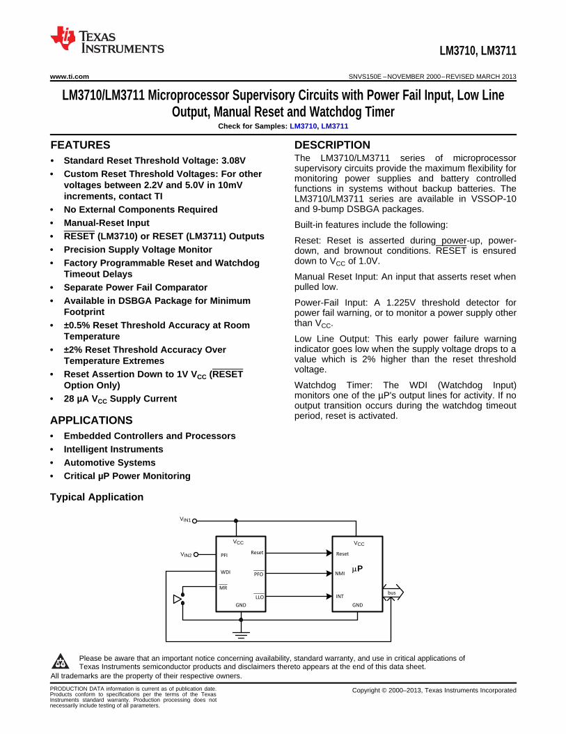
V IN1 GND GND NMI V CC PFI MR V CC PP PFO INT LLO Reset Reset V IN2 bus WDI LM3710, LM3711 www.ti.com SNVS150E – NOVEMBER 2000 – REVISED MARCH 2013 LM3710/LM3711 Microprocessor Supervisory Circuits with Power Fail Input, Low Line Output, Manual Reset and Watchdog Timer Check for Samples: LM3710, LM3711 1FEATURES DESCRIPTION The LM3710/LM3711 series of microprocessor 2• Standard Reset Threshold Voltage: 3.08V supervisory circuits provide the maximum flexibility for • Custom Reset Threshold Voltages: For other monitoring power supplies and battery controlled voltages between 2.2V and 5.0V in 10mV functions in systems without backup batteries. The increments, contact TI LM3710/LM3711 series are available in VSSOP-10 and 9-bump DSBGA packages. • No External Components Required • Manual-Reset Input Built-in features include the following: • RESET (LM3710) or RESET (LM3711) Outputs Reset: Reset is asserted during power-up, power- • Precision Supply Voltage Monitor down, and brownout conditions. RESET is ensured down to V CC of 1.0V. • Factory Programmable Reset and Watchdog Timeout Delays Manual Reset Input: An input that asserts reset when pulled low. • Separate Power Fail Comparator • Available in DSBGA Package for Minimum Power-Fail Input: A 1.225V threshold detector for Footprint power fail warning, or to monitor a power supply other than V CC . • ±0.5% Reset Threshold Accuracy at Room Temperature Low Line Output: This early power failure warning indicator goes low when the supply voltage drops to a • ±2% Reset Threshold Accuracy Over value which is 2% higher than the reset threshold Temperature Extremes voltage. • Reset Assertion Down to 1V V CC (RESET Watchdog Timer: The WDI (Watchdog Input) Option Only) monitors one of the μP's output lines for activity. If no • 28 μA V CC Supply Current output transition occurs during the watchdog timeout period, reset is activated. APPLICATIONS • Embedded Controllers and Processors • Intelligent Instruments • Automotive Systems • Critical μP Power Monitoring Typical Application 1 Please be aware that an important notice concerning availability, standard warranty, and use in critical applications of Texas Instruments semiconductor products and disclaimers thereto appears at the end of this data sheet. 2All trademarks are the property of their respective owners. PRODUCTION DATA information is current as of publication date. Copyright © 2000–2013, Texas Instruments Incorporated Products conform to specifications per the terms of the Texas Instruments standard warranty. Production processing does not necessarily include testing of all parameters.
Transcript of LM3710/LM3711 Microprocessor Supervisory Circuits … Input Current −75 75 nA (PFI only) RMR MR...
VIN1
GND GND
NMI
VCC
PFI
MR
VCC
PPPFO
INTLLO
ResetResetVIN2
bus
WDI
LM3710, LM3711
www.ti.com SNVS150E –NOVEMBER 2000–REVISED MARCH 2013
LM3710/LM3711 Microprocessor Supervisory Circuits with Power Fail Input, Low LineOutput, Manual Reset and Watchdog Timer
Check for Samples: LM3710, LM3711
1FEATURES DESCRIPTIONThe LM3710/LM3711 series of microprocessor
2• Standard Reset Threshold Voltage: 3.08Vsupervisory circuits provide the maximum flexibility for
• Custom Reset Threshold Voltages: For other monitoring power supplies and battery controlledvoltages between 2.2V and 5.0V in 10mV functions in systems without backup batteries. Theincrements, contact TI LM3710/LM3711 series are available in VSSOP-10
and 9-bump DSBGA packages.• No External Components Required• Manual-Reset Input Built-in features include the following:• RESET (LM3710) or RESET (LM3711) Outputs Reset: Reset is asserted during power-up, power-• Precision Supply Voltage Monitor down, and brownout conditions. RESET is ensured
down to VCC of 1.0V.• Factory Programmable Reset and WatchdogTimeout Delays Manual Reset Input: An input that asserts reset when
pulled low.• Separate Power Fail Comparator• Available in DSBGA Package for Minimum Power-Fail Input: A 1.225V threshold detector for
Footprint power fail warning, or to monitor a power supply otherthan VCC.• ±0.5% Reset Threshold Accuracy at Room
Temperature Low Line Output: This early power failure warningindicator goes low when the supply voltage drops to a• ±2% Reset Threshold Accuracy Overvalue which is 2% higher than the reset thresholdTemperature Extremesvoltage.• Reset Assertion Down to 1V VCC (RESETWatchdog Timer: The WDI (Watchdog Input)Option Only)monitors one of the µP's output lines for activity. If no• 28 µA VCC Supply Currentoutput transition occurs during the watchdog timeoutperiod, reset is activated.APPLICATIONS
• Embedded Controllers and Processors• Intelligent Instruments• Automotive Systems• Critical µP Power Monitoring
Typical Application
1
Please be aware that an important notice concerning availability, standard warranty, and use in critical applications ofTexas Instruments semiconductor products and disclaimers thereto appears at the end of this data sheet.
2All trademarks are the property of their respective owners.
PRODUCTION DATA information is current as of publication date. Copyright © 2000–2013, Texas Instruments IncorporatedProducts conform to specifications per the terms of the TexasInstruments standard warranty. Production processing does notnecessarily include testing of all parameters.

Reset VCC
GND WDI
MR
NC PFI
LLO
PFO
C B A
1
2
3
1
2
3
4
9
5
10
8
7
6
VCC
MR
PFI
WDI
NCGND
LLO
PFO
NC
Reset
LM3710, LM3711
SNVS150E –NOVEMBER 2000–REVISED MARCH 2013 www.ti.com
Connection Diagram
Figure 1. VSSOP-10
Figure 2. Top View(looking from the coating side)
DSBGA 9 Bump Package
PIN DESCRIPTIONSPin No.
Name FunctionDSBGA VSSOP
A1 2 MR Manual-Reset input. When MR is less than VMRT (Manual Reset Threshold) RESET/RESET isengaged.
B1 1 VCC Power Supply input.
C1 10 RESET Reset Logic Output. Pulses low for tRP (Reset Timeout Period) when triggered, and stays lowwhenever VCC is below the reset threshold or when MR is below VMRT. It remains low for tRP aftereither VCC rises above the reset threshold, or after MR input rises above VMRT (LM3710 only).
RESET Reset Logic Output. RESET is the inverse of RESET (LM3711 only).
C2 8 PFO Power-Fail Logic Output. When PFI is below VPFT, PFO goes low; otherwise, PFO remains high.
C3 7 LLO Low-Line Logic Output. Early Power-Fail warning output. Low when VCC falls below VLLOT (Low-Line Output Threshold). This output can be used to generate an NMI (Non-Maskable Interrupt) toprovide an early warning of imminent power-failure.
B3 5 GND Ground reference for all signals.
A3 4 WDI Watchdog Input Transition Monitor: If no transition activity occurs for a period exceeding tWD(Watchdog Timeout Period), reset is engaged.
A2 3 PFI Power-Fail Comparator Input. When PFI is less than VPFT (Power-Fail Reset Threshold), the PFOgoes low; otherwise, PFO remains high.
B2 6, 9 NC No Connect. Test input used at factory only. Leave floating.
2 Submit Documentation Feedback Copyright © 2000–2013, Texas Instruments Incorporated
Product Folder Links: LM3710 LM3711
LM3710, LM3711
www.ti.com SNVS150E –NOVEMBER 2000–REVISED MARCH 2013
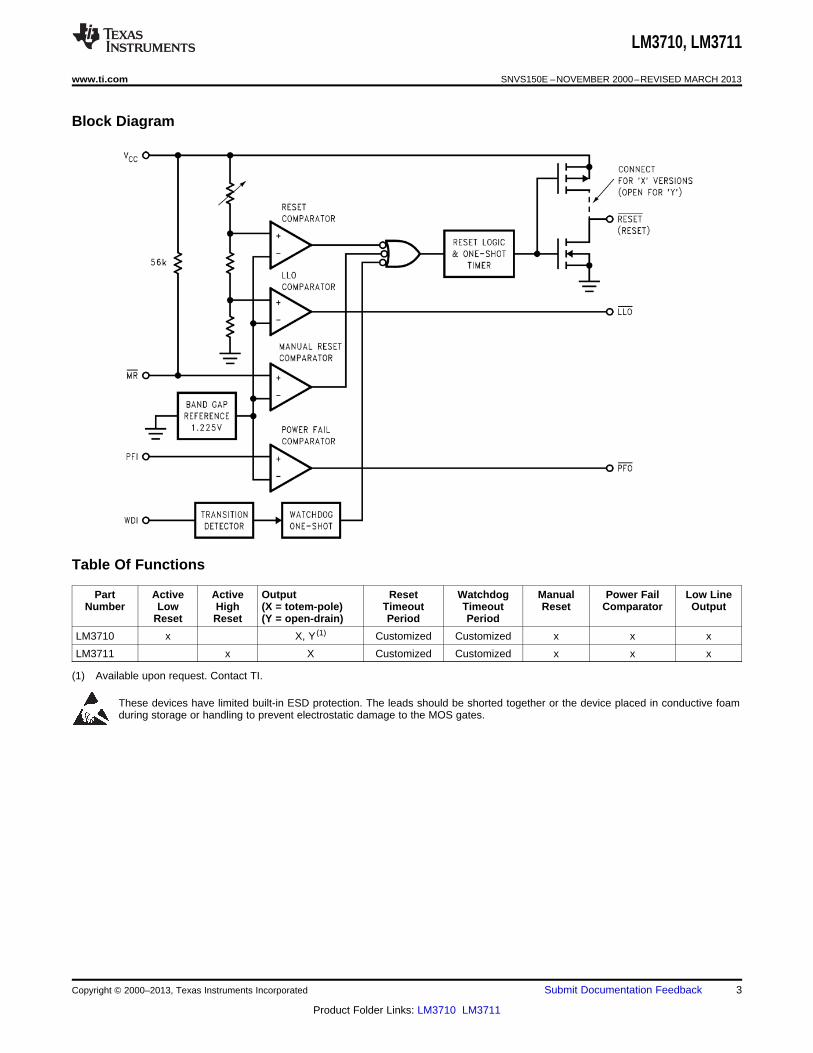
Block Diagram
Table Of Functions
Part Active Active Output Reset Watchdog Manual Power Fail Low LineNumber Low High (X = totem-pole) Timeout Timeout Reset Comparator Output
Reset Reset (Y = open-drain) Period Period
LM3710 x X, Y (1) Customized Customized x x x
LM3711 x X Customized Customized x x x
(1) Available upon request. Contact TI.
These devices have limited built-in ESD protection. The leads should be shorted together or the device placed in conductive foamduring storage or handling to prevent electrostatic damage to the MOS gates.
Copyright © 2000–2013, Texas Instruments Incorporated Submit Documentation Feedback 3
Product Folder Links: LM3710 LM3711
LM3710, LM3711
SNVS150E –NOVEMBER 2000–REVISED MARCH 2013 www.ti.com
Absolute Maximum Ratings (1) (2)
Supply Voltage (VCC) −0.3V to 6.0V
All Other Inputs −0.3V to VCC + 0.3V
ESD Ratings (3)
Human Body Model 1.5kVMachine Model 150V
Power Dissipation (4)
(1) Absolute Maximum Ratings indicate limits beyond which damage to the device may occur. Operating Ratings indicate conditions forwhich the device is intended to be functional, but do not ensure specific performance limits. For ensured specifications and testconditions, see the Electrical Characteristics. The ensured specifications apply only for the test conditions listed. Some performancecharacteristics may degrade when the device is not operated under the listed conditions.
(2) If Military/Aerospace specified devices are required, please contact the Texas Instruments Sales Office/Distributors for availability andspecifications.
(3) The Human Body model is a 100 pF capacitor discharged through a 1.5 kΩ resistor into each pin. The machine model is a 200pFcapacitor discharged directly into each pin.
(4) The maximum allowable power dissipation is a function of the maximum junction temperature, TJ(MAX), the junction-to-ambient thermalresistance, θJ-A, and the ambient temperature, TA. The maximum allowable power dissipation at any ambient temperture is calculatedusing:
Where the value of θJ-A for the VSSOP-10 package is 195°C/W in a typical PC board mounting and the DSBGA package is 220°C/W.
Operating Ratings (1)
Temperature Range −40°C ≤ TJ ≤ 85°C
(1) Absolute Maximum Ratings indicate limits beyond which damage to the device may occur. Operating Ratings indicate conditions forwhich the device is intended to be functional, but do not ensure specific performance limits. For ensured specifications and testconditions, see the Electrical Characteristics. The ensured specifications apply only for the test conditions listed. Some performancecharacteristics may degrade when the device is not operated under the listed conditions.
LM3710/LM3711 Series Electrical CharacteristicsLimits in the standard typeface are for TJ = 25°C and limits in boldface type apply over full operating range. Unless otherwisespecified: VCC = +2.2V to 5.5V.
Symbol Parameter Conditions Min Typ Max Units
POWER SUPPLY
VCC Operating Voltage LM3710 1.0 5.5VRange: VCC LM3711 1.2 5.5
ICC VCC Supply Current All inputs = VCC; all outputs floating 28 50 µA
RESET THRESHOLD
VRST Reset Threshold VCC falling −0.5 +0.5−2 +2VRST %
VCC falling: TA = 0°C to 70°C −1.5 +1.5
VRSTH Reset Threshold 0.0032•VRST mVHysteresis
tRP Reset Timeout Period Reset Timeout Period = E, J, N, S 1 1.4 2Reset Timeout Period = F, K, P, T 20 28 40 msReset Timeout Period = G, L, Q, U 140 200 280Reset Timeout Period = H, M, R, V 1120 1600 2240
tRD VCCto Reset Delay VCCfalling at 1mV/µs 20 µs
RESET (LM3711)
VOL RESET VCC > 2.25V, ISINK = 900µA 0.3
VCC > 2.7V, ISINK = 1.2mA 0.3 V
VCC > 4.5V, ISINK = 3.2mA 0.4
VOH RESET VCC > 1.2V, ISOURCE = 50µA 0.8 VCC
VCC > 1.8V, ISOURCE = 150µA 0.8 VCC
VCC > 2.25V, ISOURCE = 300µA 0.8 VCC V
VCC > 2.7V, ISOURCE = 500µA 0.8 VCC
VCC > 4.5V, ISOURCE = 800µA VCC − 1.5V
4 Submit Documentation Feedback Copyright © 2000–2013, Texas Instruments Incorporated
Product Folder Links: LM3710 LM3711
LM3710, LM3711
www.ti.com SNVS150E –NOVEMBER 2000–REVISED MARCH 2013
LM3710/LM3711 Series Electrical Characteristics (continued)Limits in the standard typeface are for TJ = 25°C and limits in boldface type apply over full operating range. Unless otherwisespecified: VCC = +2.2V to 5.5V.
Symbol Parameter Conditions Min Typ Max Units
ILKG Output Leakage VRESET = 5.5V 1.0 µACurrent
RESET (LM3710)
VOL RESET VCC > 1.0V, ISINK = 50µA 0.3
VCC > 1.2V, ISINK = 100µA 0.3
VCC > 2.25V, ISINK = 900µA 0.3
VCC > 2.7V, ISINK = 1.2mA 0.3V
VCC > 4.5V, ISINK = 3.2mA 0.4
VOH RESET VCC > 2.25V, ISOURCE = 300µA 0.8 VCC
VCC > 2.7V, ISOURCE = 500µA 0.8 VCC
VCC > 4.5V, ISOURCE = 800µA VCC − 1.5V
WDI
WDI Watchdog Input −1 +1 µACurrent
WDIT Watchdog Input 0.2•VCC 1.225 0.8•VCC VThreshold
tWD Watchdog Timeout Watchdog Timeout Period = E, F, G, H 4.3 6.2 9.3Period Watchdog Timeout Period = J, K, L, M 71 102 153 msWatchdog Timeout Period = N, P, Q, R 1120 1600 2400
Watchdog Timeout Period = S, T, U, V 17900 25600 38400
PFI/MR
VPFT PFI Input Threshold 1.200 1.225 1.250 V
VMRT MR Input Threshold MR, Low 0.8V
MR, High 2.0
VPFTH/ PFI/MR Threshold PFI/MR falling: VCC = VRST MAX to 5.5V 0.0032•VRST mVVMRTH Hysteresis
IPFI Input Current −75 75 nA(PFI only)
RMR MR Pull-up 35 56 75 kΩResistance
tMD MR to Reset Delay 12 µS
tMR MR Pulse Width 25 µS
PFO, LLO
VOL PFO, LLO Output VCC > 2.25V, ISINK = 900µA 0.3Voltage VCC > 2.7V, ISINK = 1.2mA 0.3
VCC > 4.5V, ISINK = 3.2mA 0.4V
VOH VCC > 2.25V, ISOURCE = 300µA 0.8 VCC
VCC > 2.7V, ISOURCE = 500µA 0.8 VCC
VCC > 4.5V, ISOURCE = 800µA VCC − 1.5V
LLO OUTPUT
VLLOT LLO Output 1.01•VRST 1.02•VRST 1.03•VRST VThreshold(VLLO − VRST, VCCfalling)
VLLOTH Low-Line Comparator 0.0032•VRST mVHysteresis
tCD Low-Line Comparator VCC falling at 1mV/µs 20 µsDelay
Copyright © 2000–2013, Texas Instruments Incorporated Submit Documentation Feedback 5
Product Folder Links: LM3710 LM3711
0
10
20
30
40
50
60
70
80
10 1000
Max
imum
Tra
nsie
nt D
urat
ion
(Ps)
Reset Comparator Overdrive (mV)VRST - VCC
100
190
195
200
205
210
215
-40
Temperature (°C)
Res
et T
imeo
ut P
erio
d (m
s)
25 85
Res
et T
imeo
ut P
erio
d (
ms)
Supply Voltage (V)
180
185
190
195
200
205
210
215
220
3.0 3.5 4 4.5 5 5.5 6
Nor
mal
ized
Thr
esho
ld V
olta
ge (
%)
Temperature (°C)
0.5
0.3
0.1
-0.5
-40 25 85
-0.3
-0.1
0
-0.4
-0.2
0.2
0.4
15
20
25
5
10
30
0
Supply Voltage (V)
Sup
ply
Cur
rent
(P
A)
1 2 3 4 5-40 0 25 70 85
Temperature (°C)
23
24
25
26
27
28
29
30
Sup
ply
Cur
rent
(P
A)
LM3710, LM3711
SNVS150E –NOVEMBER 2000–REVISED MARCH 2013 www.ti.com
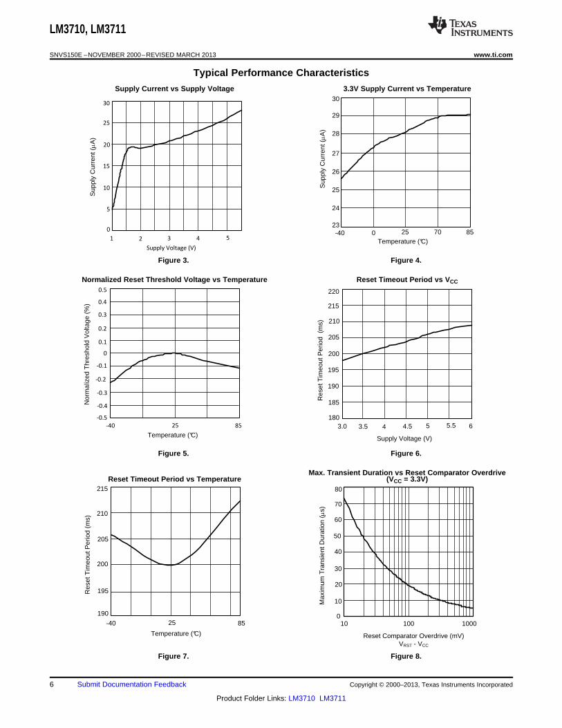
Typical Performance Characteristics
Supply Current vs Supply Voltage 3.3V Supply Current vs Temperature
Figure 3. Figure 4.
Normalized Reset Threshold Voltage vs Temperature Reset Timeout Period vs VCC
Figure 5. Figure 6.
Max. Transient Duration vs Reset Comparator OverdriveReset Timeout Period vs Temperature (VCC = 3.3V)
Figure 7. Figure 8.
6 Submit Documentation Feedback Copyright © 2000–2013, Texas Instruments Incorporated
Product Folder Links: LM3710 LM3711
5
5.2
5.4
5.6
5.8
6
6.2
6.4
6.6
6.8
7
-40 25 85
Temperature (RC)
Wa
tch
do
g T
ime
ou
t P
eri
od
(m
s)
25
27
29
31
33
35
37
39
-40 -20 0 20 40 60 80
Temperature (oC)
Pro
paga
tion
Del
ay (P
s)
LM3710, LM3711
www.ti.com SNVS150E –NOVEMBER 2000–REVISED MARCH 2013
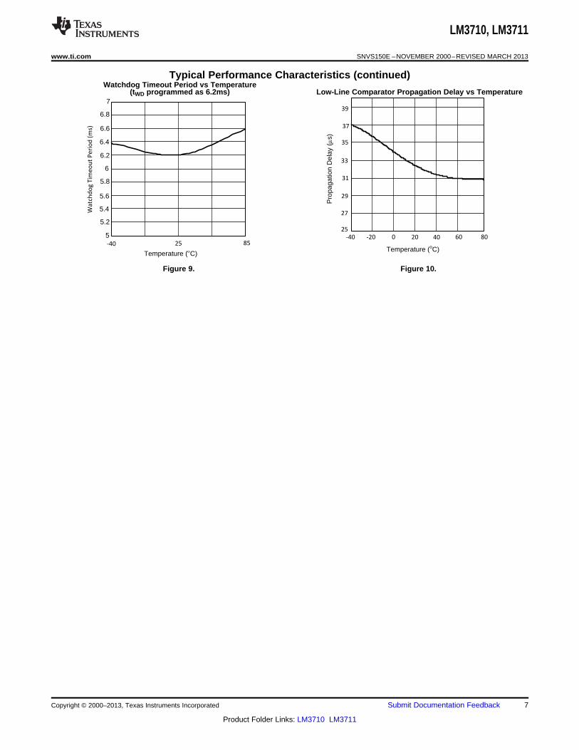
Typical Performance Characteristics (continued)Watchdog Timeout Period vs Temperature
(tWD programmed as 6.2ms) Low-Line Comparator Propagation Delay vs Temperature
Figure 9. Figure 10.
Copyright © 2000–2013, Texas Instruments Incorporated Submit Documentation Feedback 7
Product Folder Links: LM3710 LM3711
LM3710, LM3711
SNVS150E –NOVEMBER 2000–REVISED MARCH 2013 www.ti.com
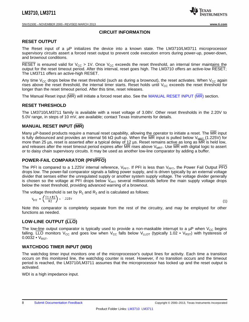
CIRCUIT INFORMATION
RESET OUTPUT
The Reset input of a µP initializes the device into a known state. The LM3710/LM3711 microprocessorsupervisory circuits assert a forced reset output to prevent code execution errors during power-up, power-down,and brownout conditions.
RESET is ensured valid for VCC > 1V. Once VCC exceeds the reset threshold, an internal timer maintains theoutput for the reset timeout period. After this interval, reset goes high. The LM3710 offers an active-low RESET;The LM3711 offers an active-high RESET.
Any time VCC drops below the reset threshold (such as during a brownout), the reset activates. When VCC againrises above the reset threshold, the internal timer starts. Reset holds until VCC exceeds the reset threshold forlonger than the reset timeout period. After this time, reset releases.
The Manual Reset input (MR) will initiate a forced reset also. See the MANUAL RESET INPUT (MR) section.
RESET THRESHOLD
The LM3710/LM3711 family is available with a reset voltage of 3.08V. Other reset thresholds in the 2.20V to5.0V range, in steps of 10 mV, are available; contact Texas Instruments for details.
MANUAL RESET INPUT (MR)
Many µP-based products require a manual reset capability, allowing the operator to initiate a reset. The MR inputis fully debounced and provides an internal 56 kΩ pull-up. When the MR input is pulled below VMRT (1.225V) formore than 25 µs, reset is asserted after a typical delay of 12 µs. Reset remains active as long as MR is held low,and releases after the reset timeout period expires after MR rises above VMRT. Use MR with digital logic to assertor to daisy chain supervisory circuits. It may be used as another low-line comparator by adding a buffer.
POWER-FAIL COMPARATOR (PFI/PFO)
The PFI is compared to a 1.225V internal reference, VPFT. If PFI is less than VPFT, the Power Fail Output PFOdrops low. The power-fail comparator signals a falling power supply, and is driven typically by an external voltagedivider that senses either the unregulated supply or another system supply voltage. The voltage divider generallyis chosen so the voltage at PFI drops below VPFT several milliseconds before the main supply voltage dropsbelow the reset threshold, providing advanced warning of a brownout.
The voltage threshold is set by R1 and R2 and is calculated as follows:
(1)
Note this comparator is completely separate from the rest of the circuitry, and may be employed for otherfunctions as needed.
LOW-LINE OUTPUT (LLO)
The low-line output comparator is typically used to provide a non-maskable interrupt to a µP when VCC beginsfalling. LLO monitors VCC and goes low when VCC falls below VLLOT (typically 1.02 • VRST) with hysteresis of0.0032 • VRST.
WATCHDOG TIMER INPUT (WDI)
The watchdog timer input monitors one of the microprocessor's output lines for activity. Each time a transitionoccurs on this monitored line, the watchdog counter is reset. However, if no transition occurs and the timeoutperiod is reached, the LM3710/LM3711 assumes that the microprocessor has locked up and the reset output isactivated.
WDI is a high impedance input.
8 Submit Documentation Feedback Copyright © 2000–2013, Texas Instruments Incorporated
Product Folder Links: LM3710 LM3711

LM3710, LM3711
www.ti.com SNVS150E –NOVEMBER 2000–REVISED MARCH 2013
SPECIAL PRECAUTIONS FOR THE DSBGA PACKAGE
As with most integrated circuits, the LM3710 and LM3711 are sensitive to exposure from visible and infrared (IR)light radiation. Unlike a plastic encapsulated IC, the DSBGA package has very limited shielding from light, andsome sensitivity to light reflected from the surface of the PC board or long wavelength IR entering the die fromthe side may be experienced. This light could have an unpredictable affect on the electrical performance of theIC. Care should be taken to shield the device from direct exposure to bright visible or IR light during operation.
DSBGA MOUNTING
The DSBGA package requires specific mounting techniques which are detailed in TI Application Note AN-1112(SNVA009). Referring to the section Surface Mount Assembly Considerations, it should be noted that the padstyle which must be used with the 9-pin package is the NSMD (non-solder mask defined) type.
For best results during assembly, alignment ordinals on the PC board may be used to facilitate placement of theDSBGA device.
Timing Diagrams
Figure 11. LM3710/LM3711 Reset Time with MR and WDI
Figure 12. LLO Output
Copyright © 2000–2013, Texas Instruments Incorporated Submit Documentation Feedback 9
Product Folder Links: LM3710 LM3711
GND GND
VCC
PFI
PPINT
R1
R2
RESETRESET
LLO
PFOMR
VIN1VIN2
Active Data Line
WDI
R2
+ 1Power-Fail Reset Threshold, VPFT = 1.225 (
(. R1
LM3710, LM3711
SNVS150E –NOVEMBER 2000–REVISED MARCH 2013 www.ti.com
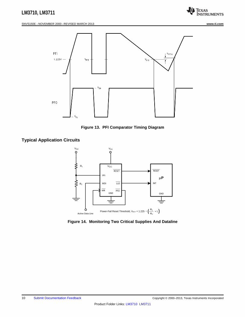
Figure 13. PFI Comparator Timing Diagram
Typical Application Circuits
Figure 14. Monitoring Two Critical Supplies And Dataline
10 Submit Documentation Feedback Copyright © 2000–2013, Texas Instruments Incorporated
Product Folder Links: LM3710 LM3711
System
Regulator0.1Pceramic
3.3V
R1
R2
VCC
GND
PFI
RESETMR
PFO
RESET
INTPP
R1
R2
+ 1Power-Fail Reset Threshold, VPFT = 1.225 (
(.
Raw Supply
(Battery)
Active Data
Line
WDI
VCC
RESET
3.3V
1.8V
107k
332k
VI/O VCORE
FAULT (Normally High)
GND
PFI
PFO
RESET
Active Data Line
WDI
MR
GND
VCC
PFI
MR PFO
RESETRESET
3.3V1.8V
107k
332k
VI/O Vcore
3.3k
WDI
Active Data Line
LM3710, LM3711
www.ti.com SNVS150E –NOVEMBER 2000–REVISED MARCH 2013
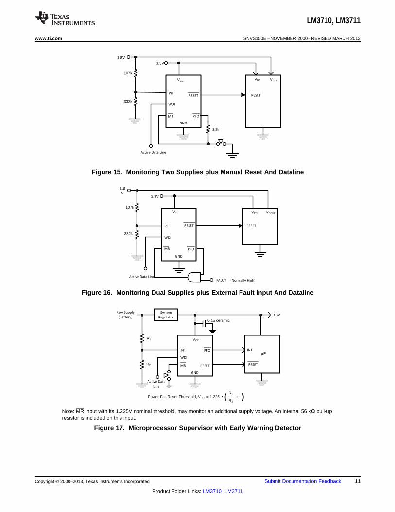
Figure 15. Monitoring Two Supplies plus Manual Reset And Dataline
Figure 16. Monitoring Dual Supplies plus External Fault Input And Dataline
Note: MR input with its 1.225V nominal threshold, may monitor an additional supply voltage. An internal 56 kΩ pull-upresistor is included on this input.
Figure 17. Microprocessor Supervisor with Early Warning Detector
Copyright © 2000–2013, Texas Instruments Incorporated Submit Documentation Feedback 11
Product Folder Links: LM3710 LM3711
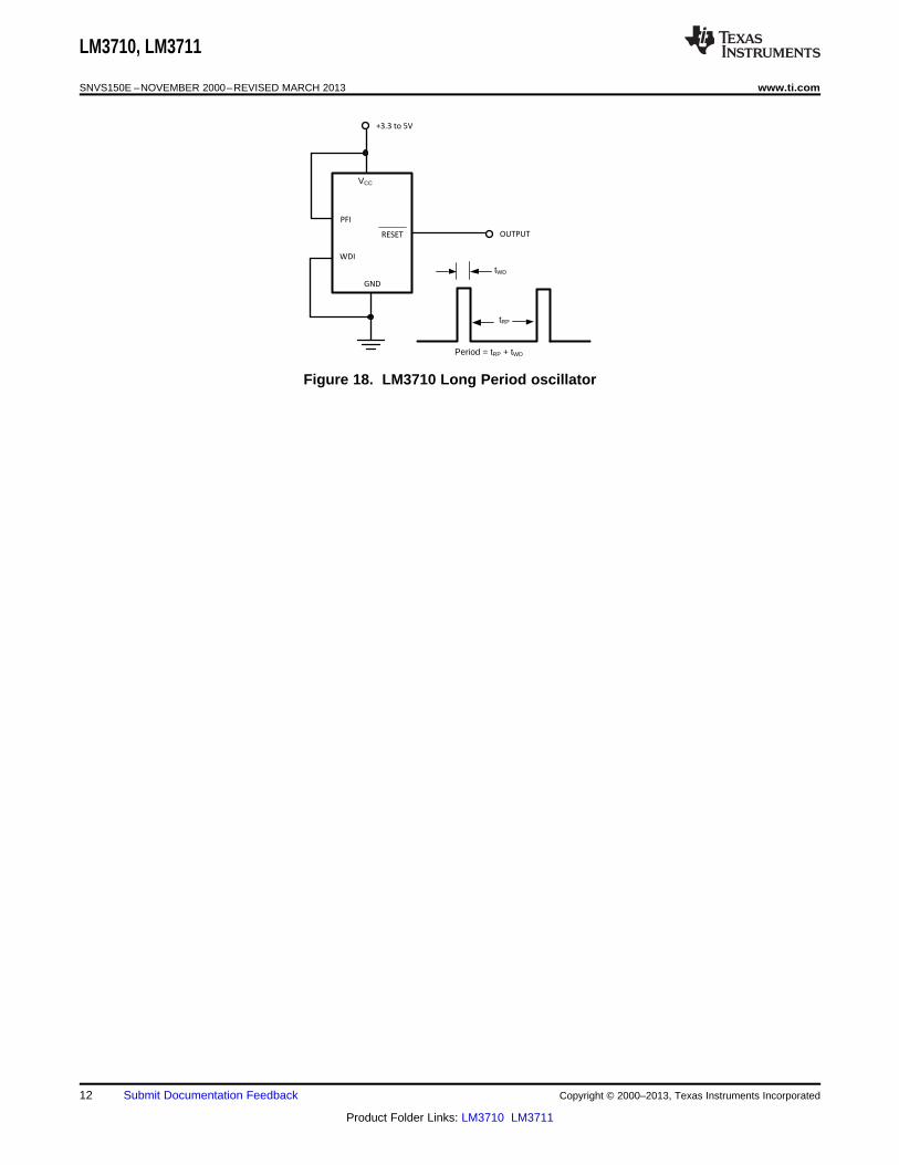
VCC
GND
PFI
RESET
WDI
OUTPUT
+3.3 to 5V
tRP
tWD
Period = tRP + tWD
LM3710, LM3711
SNVS150E –NOVEMBER 2000–REVISED MARCH 2013 www.ti.com
Figure 18. LM3710 Long Period oscillator
12 Submit Documentation Feedback Copyright © 2000–2013, Texas Instruments Incorporated
Product Folder Links: LM3710 LM3711
LM3710, LM3711
www.ti.com SNVS150E –NOVEMBER 2000–REVISED MARCH 2013
REVISION HISTORY
Changes from Revision D (March 2013) to Revision E Page
• Changed layout of National Data Sheet to TI format .......................................................................................................... 12
Copyright © 2000–2013, Texas Instruments Incorporated Submit Documentation Feedback 13
Product Folder Links: LM3710 LM3711
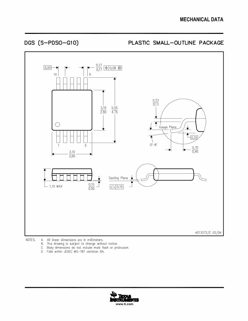
PACKAGE OPTION ADDENDUM
www.ti.com 8-Oct-2015
Addendum-Page 1
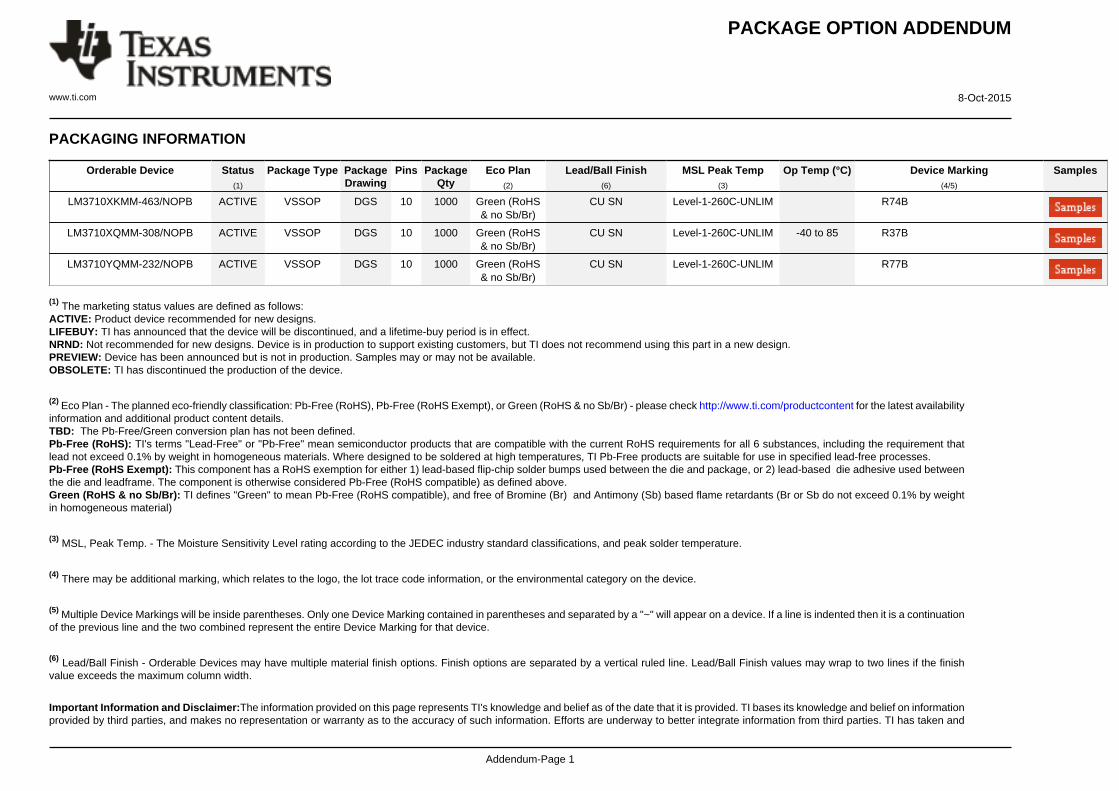
PACKAGING INFORMATION
Orderable Device Status(1)
Package Type PackageDrawing
Pins PackageQty
Eco Plan(2)
Lead/Ball Finish(6)
MSL Peak Temp(3)
Op Temp (°C) Device Marking(4/5)
Samples
LM3710XKMM-463/NOPB ACTIVE VSSOP DGS 10 1000 Green (RoHS& no Sb/Br)
CU SN Level-1-260C-UNLIM R74B
LM3710XQMM-308/NOPB ACTIVE VSSOP DGS 10 1000 Green (RoHS& no Sb/Br)
CU SN Level-1-260C-UNLIM -40 to 85 R37B
LM3710YQMM-232/NOPB ACTIVE VSSOP DGS 10 1000 Green (RoHS& no Sb/Br)
CU SN Level-1-260C-UNLIM R77B
(1) The marketing status values are defined as follows:ACTIVE: Product device recommended for new designs.LIFEBUY: TI has announced that the device will be discontinued, and a lifetime-buy period is in effect.NRND: Not recommended for new designs. Device is in production to support existing customers, but TI does not recommend using this part in a new design.PREVIEW: Device has been announced but is not in production. Samples may or may not be available.OBSOLETE: TI has discontinued the production of the device.
(2) Eco Plan - The planned eco-friendly classification: Pb-Free (RoHS), Pb-Free (RoHS Exempt), or Green (RoHS & no Sb/Br) - please check http://www.ti.com/productcontent for the latest availabilityinformation and additional product content details.TBD: The Pb-Free/Green conversion plan has not been defined.Pb-Free (RoHS): TI's terms "Lead-Free" or "Pb-Free" mean semiconductor products that are compatible with the current RoHS requirements for all 6 substances, including the requirement thatlead not exceed 0.1% by weight in homogeneous materials. Where designed to be soldered at high temperatures, TI Pb-Free products are suitable for use in specified lead-free processes.Pb-Free (RoHS Exempt): This component has a RoHS exemption for either 1) lead-based flip-chip solder bumps used between the die and package, or 2) lead-based die adhesive used betweenthe die and leadframe. The component is otherwise considered Pb-Free (RoHS compatible) as defined above.Green (RoHS & no Sb/Br): TI defines "Green" to mean Pb-Free (RoHS compatible), and free of Bromine (Br) and Antimony (Sb) based flame retardants (Br or Sb do not exceed 0.1% by weightin homogeneous material)
(3) MSL, Peak Temp. - The Moisture Sensitivity Level rating according to the JEDEC industry standard classifications, and peak solder temperature.
(4) There may be additional marking, which relates to the logo, the lot trace code information, or the environmental category on the device.
(5) Multiple Device Markings will be inside parentheses. Only one Device Marking contained in parentheses and separated by a "~" will appear on a device. If a line is indented then it is a continuationof the previous line and the two combined represent the entire Device Marking for that device.
(6) Lead/Ball Finish - Orderable Devices may have multiple material finish options. Finish options are separated by a vertical ruled line. Lead/Ball Finish values may wrap to two lines if the finishvalue exceeds the maximum column width.
Important Information and Disclaimer:The information provided on this page represents TI's knowledge and belief as of the date that it is provided. TI bases its knowledge and belief on informationprovided by third parties, and makes no representation or warranty as to the accuracy of such information. Efforts are underway to better integrate information from third parties. TI has taken and
PACKAGE OPTION ADDENDUM
www.ti.com 8-Oct-2015
Addendum-Page 2
continues to take reasonable steps to provide representative and accurate information but may not have conducted destructive testing or chemical analysis on incoming materials and chemicals.TI and TI suppliers consider certain information to be proprietary, and thus CAS numbers and other limited information may not be available for release.
In no event shall TI's liability arising out of such information exceed the total purchase price of the TI part(s) at issue in this document sold by TI to Customer on an annual basis.
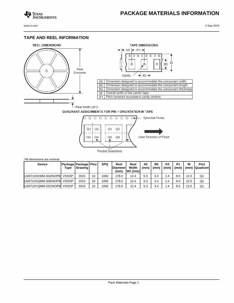
TAPE AND REEL INFORMATION
*All dimensions are nominal
Device PackageType
PackageDrawing
Pins SPQ ReelDiameter
(mm)
ReelWidth
W1 (mm)
A0(mm)
B0(mm)
K0(mm)
P1(mm)
W(mm)
Pin1Quadrant
LM3710XKMM-463/NOPB VSSOP DGS 10 1000 178.0 12.4 5.3 3.4 1.4 8.0 12.0 Q1
LM3710XQMM-308/NOPB VSSOP DGS 10 1000 178.0 12.4 5.3 3.4 1.4 8.0 12.0 Q1
LM3710YQMM-232/NOPB VSSOP DGS 10 1000 178.0 12.4 5.3 3.4 1.4 8.0 12.0 Q1
PACKAGE MATERIALS INFORMATION
www.ti.com 2-Sep-2015
Pack Materials-Page 1
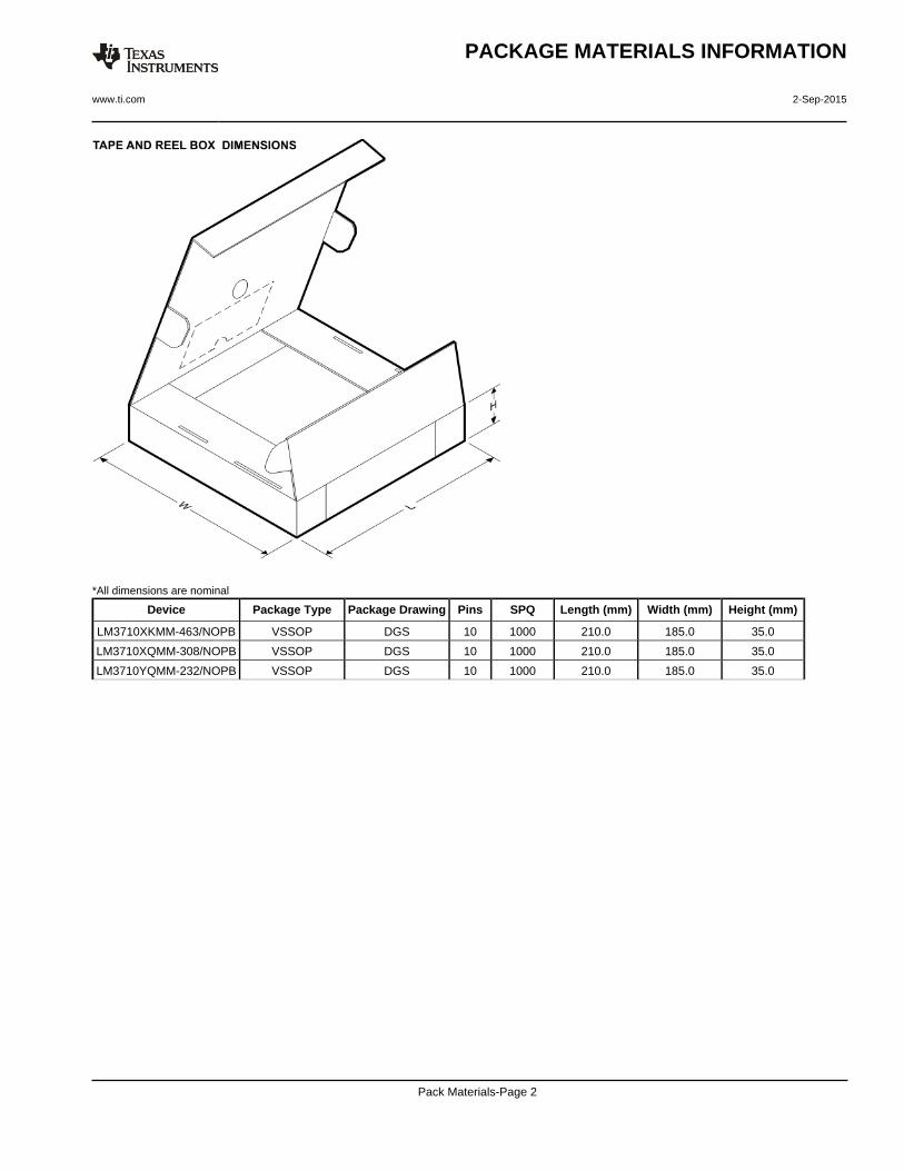
*All dimensions are nominal
Device Package Type Package Drawing Pins SPQ Length (mm) Width (mm) Height (mm)
LM3710XKMM-463/NOPB VSSOP DGS 10 1000 210.0 185.0 35.0
LM3710XQMM-308/NOPB VSSOP DGS 10 1000 210.0 185.0 35.0
LM3710YQMM-232/NOPB VSSOP DGS 10 1000 210.0 185.0 35.0
PACKAGE MATERIALS INFORMATION
www.ti.com 2-Sep-2015
Pack Materials-Page 2
IMPORTANT NOTICE
Texas Instruments Incorporated and its subsidiaries (TI) reserve the right to make corrections, enhancements, improvements and otherchanges to its semiconductor products and services per JESD46, latest issue, and to discontinue any product or service per JESD48, latestissue. Buyers should obtain the latest relevant information before placing orders and should verify that such information is current andcomplete. All semiconductor products (also referred to herein as “components”) are sold subject to TI’s terms and conditions of salesupplied at the time of order acknowledgment.TI warrants performance of its components to the specifications applicable at the time of sale, in accordance with the warranty in TI’s termsand conditions of sale of semiconductor products. Testing and other quality control techniques are used to the extent TI deems necessaryto support this warranty. Except where mandated by applicable law, testing of all parameters of each component is not necessarilyperformed.TI assumes no liability for applications assistance or the design of Buyers’ products. Buyers are responsible for their products andapplications using TI components. To minimize the risks associated with Buyers’ products and applications, Buyers should provideadequate design and operating safeguards.TI does not warrant or represent that any license, either express or implied, is granted under any patent right, copyright, mask work right, orother intellectual property right relating to any combination, machine, or process in which TI components or services are used. Informationpublished by TI regarding third-party products or services does not constitute a license to use such products or services or a warranty orendorsement thereof. Use of such information may require a license from a third party under the patents or other intellectual property of thethird party, or a license from TI under the patents or other intellectual property of TI.Reproduction of significant portions of TI information in TI data books or data sheets is permissible only if reproduction is without alterationand is accompanied by all associated warranties, conditions, limitations, and notices. TI is not responsible or liable for such altereddocumentation. Information of third parties may be subject to additional restrictions.Resale of TI components or services with statements different from or beyond the parameters stated by TI for that component or servicevoids all express and any implied warranties for the associated TI component or service and is an unfair and deceptive business practice.TI is not responsible or liable for any such statements.Buyer acknowledges and agrees that it is solely responsible for compliance with all legal, regulatory and safety-related requirementsconcerning its products, and any use of TI components in its applications, notwithstanding any applications-related information or supportthat may be provided by TI. Buyer represents and agrees that it has all the necessary expertise to create and implement safeguards whichanticipate dangerous consequences of failures, monitor failures and their consequences, lessen the likelihood of failures that might causeharm and take appropriate remedial actions. Buyer will fully indemnify TI and its representatives against any damages arising out of the useof any TI components in safety-critical applications.In some cases, TI components may be promoted specifically to facilitate safety-related applications. With such components, TI’s goal is tohelp enable customers to design and create their own end-product solutions that meet applicable functional safety standards andrequirements. Nonetheless, such components are subject to these terms.No TI components are authorized for use in FDA Class III (or similar life-critical medical equipment) unless authorized officers of the partieshave executed a special agreement specifically governing such use.Only those TI components which TI has specifically designated as military grade or “enhanced plastic” are designed and intended for use inmilitary/aerospace applications or environments. Buyer acknowledges and agrees that any military or aerospace use of TI componentswhich have not been so designated is solely at the Buyer's risk, and that Buyer is solely responsible for compliance with all legal andregulatory requirements in connection with such use.TI has specifically designated certain components as meeting ISO/TS16949 requirements, mainly for automotive use. In any case of use ofnon-designated products, TI will not be responsible for any failure to meet ISO/TS16949.
Products ApplicationsAudio www.ti.com/audio Automotive and Transportation www.ti.com/automotiveAmplifiers amplifier.ti.com Communications and Telecom www.ti.com/communicationsData Converters dataconverter.ti.com Computers and Peripherals www.ti.com/computersDLP® Products www.dlp.com Consumer Electronics www.ti.com/consumer-appsDSP dsp.ti.com Energy and Lighting www.ti.com/energyClocks and Timers www.ti.com/clocks Industrial www.ti.com/industrialInterface interface.ti.com Medical www.ti.com/medicalLogic logic.ti.com Security www.ti.com/securityPower Mgmt power.ti.com Space, Avionics and Defense www.ti.com/space-avionics-defenseMicrocontrollers microcontroller.ti.com Video and Imaging www.ti.com/videoRFID www.ti-rfid.comOMAP Applications Processors www.ti.com/omap TI E2E Community e2e.ti.comWireless Connectivity www.ti.com/wirelessconnectivity
Mailing Address: Texas Instruments, Post Office Box 655303, Dallas, Texas 75265Copyright © 2016, Texas Instruments Incorporated
![micRun - Productivity Inc · 3/4* 19.05 1132.19056 MR 11- 32 DIN 6499 ISO 1/ 5488 MR Metric Collets MR Inch Collets 4. MR REGO-FIX.COM 800-999-7346 Type Part No. D [mm] L [mm] BT](https://static.fdocument.org/doc/165x107/614375096b2ee0265c020ed5/micrun-productivity-inc-34-1905-113219056-mr-11-32-din-6499-iso-1-5488-mr.jpg)