LM10 Operational Amplifier and Voltage Reference (Rev. C)
32
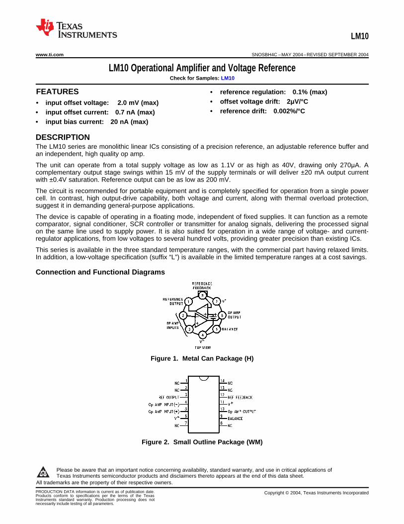
LM10 www.ti.com SNOSBH4C – MAY 2004 – REVISED SEPTEMBER 2004 LM10 Operational Amplifier and Voltage Reference Check for Samples: LM10 1FEATURES • reference regulation: 0.1% (max) • offset voltage drift: 2μV/°C 2• input offset voltage: 2.0 mV (max) • reference drift: 0.002%/°C • input offset current: 0.7 nA (max) • input bias current: 20 nA (max) DESCRIPTION The LM10 series are monolithic linear ICs consisting of a precision reference, an adjustable reference buffer and an independent, high quality op amp. The unit can operate from a total supply voltage as low as 1.1V or as high as 40V, drawing only 270μA. A complementary output stage swings within 15 mV of the supply terminals or will deliver ±20 mA output current with ±0.4V saturation. Reference output can be as low as 200 mV. The circuit is recommended for portable equipment and is completely specified for operation from a single power cell. In contrast, high output-drive capability, both voltage and current, along with thermal overload protection, suggest it in demanding general-purpose applications. The device is capable of operating in a floating mode, independent of fixed supplies. It can function as a remote comparator, signal conditioner, SCR controller or transmitter for analog signals, delivering the processed signal on the same line used to supply power. It is also suited for operation in a wide range of voltage- and current- regulator applications, from low voltages to several hundred volts, providing greater precision than existing ICs. This series is available in the three standard temperature ranges, with the commercial part having relaxed limits. In addition, a low-voltage specification (suffix “L”) is available in the limited temperature ranges at a cost savings. Connection and Functional Diagrams Figure 1. Metal Can Package (H) Figure 2. Small Outline Package (WM) 1 Please be aware that an important notice concerning availability, standard warranty, and use in critical applications of Texas Instruments semiconductor products and disclaimers thereto appears at the end of this data sheet. 2All trademarks are the property of their respective owners. PRODUCTION DATA information is current as of publication date. Copyright © 2004, Texas Instruments Incorporated Products conform to specifications per the terms of the Texas Instruments standard warranty. Production processing does not necessarily include testing of all parameters.
Transcript of LM10 Operational Amplifier and Voltage Reference (Rev. C)
LM10
www.ti.com SNOSBH4C –MAY 2004–REVISED SEPTEMBER 2004
LM10 Operational Amplifier and Voltage ReferenceCheck for Samples: LM10
1FEATURES • reference regulation: 0.1% (max)• offset voltage drift: 2μV/°C
2• input offset voltage: 2.0 mV (max)• reference drift: 0.002%/°C• input offset current: 0.7 nA (max)
• input bias current: 20 nA (max)
DESCRIPTIONThe LM10 series are monolithic linear ICs consisting of a precision reference, an adjustable reference buffer andan independent, high quality op amp.
The unit can operate from a total supply voltage as low as 1.1V or as high as 40V, drawing only 270μA. Acomplementary output stage swings within 15 mV of the supply terminals or will deliver ±20 mA output currentwith ±0.4V saturation. Reference output can be as low as 200 mV.
The circuit is recommended for portable equipment and is completely specified for operation from a single powercell. In contrast, high output-drive capability, both voltage and current, along with thermal overload protection,suggest it in demanding general-purpose applications.
The device is capable of operating in a floating mode, independent of fixed supplies. It can function as a remotecomparator, signal conditioner, SCR controller or transmitter for analog signals, delivering the processed signalon the same line used to supply power. It is also suited for operation in a wide range of voltage- and current-regulator applications, from low voltages to several hundred volts, providing greater precision than existing ICs.
This series is available in the three standard temperature ranges, with the commercial part having relaxed limits.In addition, a low-voltage specification (suffix “L”) is available in the limited temperature ranges at a cost savings.
Connection and Functional Diagrams
Figure 1. Metal Can Package (H)
Figure 2. Small Outline Package (WM)
1
Please be aware that an important notice concerning availability, standard warranty, and use in critical applications ofTexas Instruments semiconductor products and disclaimers thereto appears at the end of this data sheet.
2All trademarks are the property of their respective owners.
PRODUCTION DATA information is current as of publication date. Copyright © 2004, Texas Instruments IncorporatedProducts conform to specifications per the terms of the TexasInstruments standard warranty. Production processing does notnecessarily include testing of all parameters.
LM10
SNOSBH4C –MAY 2004–REVISED SEPTEMBER 2004 www.ti.com
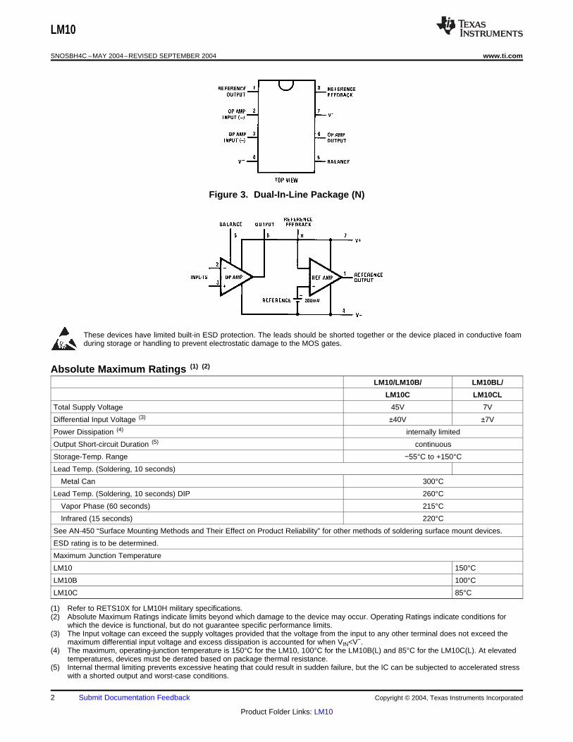
Figure 3. Dual-In-Line Package (N)
These devices have limited built-in ESD protection. The leads should be shorted together or the device placed in conductive foamduring storage or handling to prevent electrostatic damage to the MOS gates.
Absolute Maximum Ratings (1) (2)
LM10/LM10B/ LM10BL/
LM10C LM10CL
Total Supply Voltage 45V 7V
Differential Input Voltage (3) ±40V ±7V
Power Dissipation (4) internally limited
Output Short-circuit Duration (5) continuous
Storage-Temp. Range −55°C to +150°C
Lead Temp. (Soldering, 10 seconds)
Metal Can 300°C
Lead Temp. (Soldering, 10 seconds) DIP 260°C
Vapor Phase (60 seconds) 215°C
Infrared (15 seconds) 220°C
See AN-450 “Surface Mounting Methods and Their Effect on Product Reliability” for other methods of soldering surface mount devices.
ESD rating is to be determined.
Maximum Junction Temperature
LM10 150°C
LM10B 100°C
LM10C 85°C
(1) Refer to RETS10X for LM10H military specifications.(2) Absolute Maximum Ratings indicate limits beyond which damage to the device may occur. Operating Ratings indicate conditions for
which the device is functional, but do not guarantee specific performance limits.(3) The Input voltage can exceed the supply voltages provided that the voltage from the input to any other terminal does not exceed the
maximum differential input voltage and excess dissipation is accounted for when VIN<V−.(4) The maximum, operating-junction temperature is 150°C for the LM10, 100°C for the LM10B(L) and 85°C for the LM10C(L). At elevated
temperatures, devices must be derated based on package thermal resistance.(5) Internal thermal limiting prevents excessive heating that could result in sudden failure, but the IC can be subjected to accelerated stress
with a shorted output and worst-case conditions.
2 Submit Documentation Feedback Copyright © 2004, Texas Instruments Incorporated
Product Folder Links: LM10
LM10
www.ti.com SNOSBH4C –MAY 2004–REVISED SEPTEMBER 2004
Operating RatingsPackage Thermal Resistance
θJA
H Package 150°C/W
N Package 87°C/W
WM Package 90°C/W
θJC
H Package 45°C/W
Copyright © 2004, Texas Instruments Incorporated Submit Documentation Feedback 3
Product Folder Links: LM10
LM10
SNOSBH4C –MAY 2004–REVISED SEPTEMBER 2004 www.ti.com
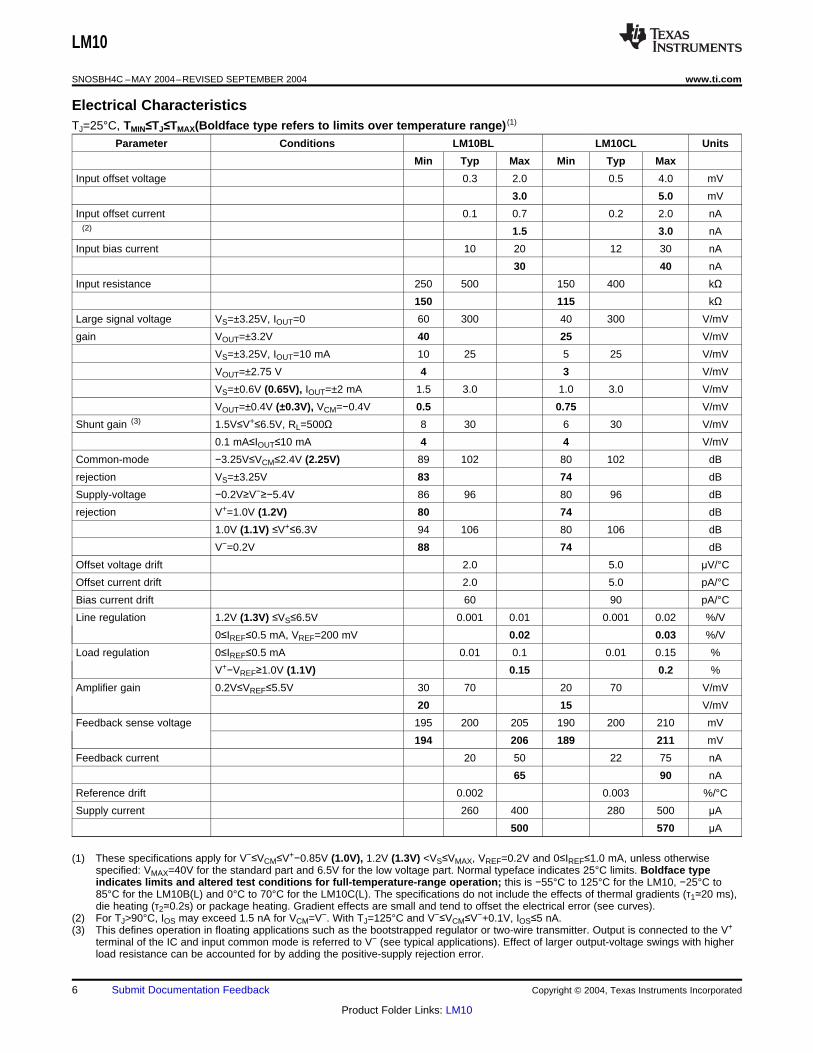
Electrical CharacteristicsTJ=25°C, TMIN≤TJ≤TMAX(Boldface type refers to limits over temperature range) (1)
Parameter Conditions LM10/LM10B LM10C Units
Min Typ Max Min Typ Max
Input offset voltage 0.3 2.0 0.5 4.0 mV
3.0 5.0 mV
Input offset current 0.25 0.7 0.4 2.0 nA(2) 1.5 3.0 nA
Input bias current 10 20 12 30 nA
30 40 nA
Input resistance 250 500 150 400 kΩ150 115 kΩ
Large signal voltage VS=±20V, IOUT=0 120 400 80 400 V/mV
gain VOUT=±19.95V 80 50 V/mV
VS=±20V, VOUT=±19.4V 50 130 25 130 V/mV
IOUT=±20 mA (±15 mA) 20 15 V/mV
VS=±0.6V (0.65V), IOUT=±2 mA 1.5 3.0 1.0 3.0 V/mV
VOUT=±0.4V (±0.3V), VCM=−0.4V 0.5 0.75 V/mV
Shunt gain (3) 1.2V (1.3V) ≤VOUT≤40V, 14 33 10 33 V/mV
RL=1.1 kΩ0.1 mA≤IOUT≤5 mA 6 6 V/mV
1.5V≤V+≤40V, RL=250Ω 8 25 6 25 V/mV
0.1 mA≤IOUT≤20 mA 4 4 V/mV
Common-mode −20V≤VCM≤19.15V (19V) 93 102 90 102 dB
rejection VS=±20V 87 87 dB
Supply-voltage −0.2V≥V−≥−39V 90 96 87 96 dB
rejection V+=1.0V (1.1V) 84 84 dB
1.0V (1.1V) ≤V+≤39.8V 96 106 93 106 dB
V−=−0.2V 90 90 dB
Offset voltage drift 2.0 5.0 μV/°C
Offset current drift 2.0 5.0 pA/°C
Bias current drift TC<100°C 60 90 pA/°C
Line regulation 1.2V (1.3V) ≤VS≤40V 0.001 0.003 0.001 0.008 %/V
0≤IREF≤1.0 mA, VREF=200 mV 0.006 0.01 %/V
Load regulation 0≤IREF≤1.0 mA 0.01 0.1 0.01 0.15 %
V+−VREF≥1.0V (1.1V) 0.15 0.2 %
Amplifier gain 0.2V≤VREF≤35V 50 75 25 70 V/mV
23 15 V/mV
Feedback sense 195 200 205 190 200 210 mV
voltage 194 206 189 211 mV
Feedback current 20 50 22 75 nA
65 90 nA
Reference drift 0.002 0.003 %/°C
(1) These specifications apply for V−≤VCM≤V+−0.85V (1.0V), 1.2V (1.3V) <VS≤VMAX, VREF=0.2V and 0≤IREF≤1.0 mA, unless otherwisespecified: VMAX=40V for the standard part and 6.5V for the low voltage part. Normal typeface indicates 25°C limits. Boldface typeindicates limits and altered test conditions for full-temperature-range operation; this is −55°C to 125°C for the LM10, −25°C to85°C for the LM10B(L) and 0°C to 70°C for the LM10C(L). The specifications do not include the effects of thermal gradients (τ1≃20 ms),die heating (τ2≃0.2s) or package heating. Gradient effects are small and tend to offset the electrical error (see curves).
(2) For TJ>90°C, IOS may exceed 1.5 nA for VCM=V−. With TJ=125°C and V−≤VCM≤V−+0.1V, IOS≤5 nA.(3) This defines operation in floating applications such as the bootstrapped regulator or two-wire transmitter. Output is connected to the V+
terminal of the IC and input common mode is referred to V− (see typical applications). Effect of larger output-voltage swings with higherload resistance can be accounted for by adding the positive-supply rejection error.
4 Submit Documentation Feedback Copyright © 2004, Texas Instruments Incorporated
Product Folder Links: LM10
LM10
www.ti.com SNOSBH4C –MAY 2004–REVISED SEPTEMBER 2004
Electrical Characteristics (continued)TJ=25°C, TMIN≤TJ≤TMAX(Boldface type refers to limits over temperature range)(1)
Parameter Conditions LM10/LM10B LM10C Units
Min Typ Max Min Typ Max
Supply current 270 400 300 500 μA
500 570 μA
Supply current change 1.2V (1.3V) ≤VS≤40V 15 75 15 75 μA
Copyright © 2004, Texas Instruments Incorporated Submit Documentation Feedback 5
Product Folder Links: LM10
LM10
SNOSBH4C –MAY 2004–REVISED SEPTEMBER 2004 www.ti.com
Electrical CharacteristicsTJ=25°C, TMIN≤TJ≤TMAX(Boldface type refers to limits over temperature range) (1)
Parameter Conditions LM10BL LM10CL Units
Min Typ Max Min Typ Max
Input offset voltage 0.3 2.0 0.5 4.0 mV
3.0 5.0 mV
Input offset current 0.1 0.7 0.2 2.0 nA(2) 1.5 3.0 nA
Input bias current 10 20 12 30 nA
30 40 nA
Input resistance 250 500 150 400 kΩ150 115 kΩ
Large signal voltage VS=±3.25V, IOUT=0 60 300 40 300 V/mV
gain VOUT=±3.2V 40 25 V/mV
VS=±3.25V, IOUT=10 mA 10 25 5 25 V/mV
VOUT=±2.75 V 4 3 V/mV
VS=±0.6V (0.65V), IOUT=±2 mA 1.5 3.0 1.0 3.0 V/mV
VOUT=±0.4V (±0.3V), VCM=−0.4V 0.5 0.75 V/mV
Shunt gain (3) 1.5V≤V+≤6.5V, RL=500Ω 8 30 6 30 V/mV
0.1 mA≤IOUT≤10 mA 4 4 V/mV
Common-mode −3.25V≤VCM≤2.4V (2.25V) 89 102 80 102 dB
rejection VS=±3.25V 83 74 dB
Supply-voltage −0.2V≥V−≥−5.4V 86 96 80 96 dB
rejection V+=1.0V (1.2V) 80 74 dB
1.0V (1.1V) ≤V+≤6.3V 94 106 80 106 dB
V−=0.2V 88 74 dB
Offset voltage drift 2.0 5.0 μV/°C
Offset current drift 2.0 5.0 pA/°C
Bias current drift 60 90 pA/°C
Line regulation 1.2V (1.3V) ≤VS≤6.5V 0.001 0.01 0.001 0.02 %/V
0≤IREF≤0.5 mA, VREF=200 mV 0.02 0.03 %/V
Load regulation 0≤IREF≤0.5 mA 0.01 0.1 0.01 0.15 %
V+−VREF≥1.0V (1.1V) 0.15 0.2 %
Amplifier gain 0.2V≤VREF≤5.5V 30 70 20 70 V/mV
20 15 V/mV
Feedback sense voltage 195 200 205 190 200 210 mV
194 206 189 211 mV
Feedback current 20 50 22 75 nA
65 90 nA
Reference drift 0.002 0.003 %/°C
Supply current 260 400 280 500 μA
500 570 μA
(1) These specifications apply for V−≤VCM≤V+−0.85V (1.0V), 1.2V (1.3V) <VS≤VMAX, VREF=0.2V and 0≤IREF≤1.0 mA, unless otherwisespecified: VMAX=40V for the standard part and 6.5V for the low voltage part. Normal typeface indicates 25°C limits. Boldface typeindicates limits and altered test conditions for full-temperature-range operation; this is −55°C to 125°C for the LM10, −25°C to85°C for the LM10B(L) and 0°C to 70°C for the LM10C(L). The specifications do not include the effects of thermal gradients (τ1≃20 ms),die heating (τ2≃0.2s) or package heating. Gradient effects are small and tend to offset the electrical error (see curves).
(2) For TJ>90°C, IOS may exceed 1.5 nA for VCM=V−. With TJ=125°C and V−≤VCM≤V−+0.1V, IOS≤5 nA.(3) This defines operation in floating applications such as the bootstrapped regulator or two-wire transmitter. Output is connected to the V+
terminal of the IC and input common mode is referred to V− (see typical applications). Effect of larger output-voltage swings with higherload resistance can be accounted for by adding the positive-supply rejection error.
6 Submit Documentation Feedback Copyright © 2004, Texas Instruments Incorporated
Product Folder Links: LM10
LM10
www.ti.com SNOSBH4C –MAY 2004–REVISED SEPTEMBER 2004
Definition of Terms
Input offset voltage: That voltage which must be applied between the input terminals to bias the unloaded output in thelinear region.Input offset current: The difference in the currents at the input terminals when the unloaded output is in the linear region.Input bias current: The absolute value of the average of the two input currents.Input resistance: The ratio of the change in input voltage to the change in input current on either input with the othergrounded.Large signal voltage gain: The ratio of the specified output voltage swing to the change in differential input voltage requiredto produce it.Shunt gain: The ratio of the specified output voltage swing to the change in differential input voltage required to produce itwith the output tied to the V+ terminal of the IC. The load and power source are connected between the V+ and V− terminals,and input common-mode is referred to the V− terminal.Common-mode rejection: The ratio of the input voltage range to the change in offset voltage between the extremes.Supply-voltage rejection: The ratio of the specified supply-voltage change to the change in offset voltage between theextremes.Line regulation: The average change in reference output voltage over the specified supply voltage range.Load regulation: The change in reference output voltage from no load to that load specified.Feedback sense voltage: The voltage, referred to V−, on the reference feedback terminal while operating in regulation.Reference amplifier gain: The ratio of the specified reference output change to the change in feedback sense voltagerequired to produce it.Feedback current: The absolute value of the current at the feedback terminal when operating in regulation.Supply current: The current required from the power source to operate the amplifier and reference with their outputsunloaded and operating in the linear range.
Copyright © 2004, Texas Instruments Incorporated Submit Documentation Feedback 7
Product Folder Links: LM10
LM10
SNOSBH4C –MAY 2004–REVISED SEPTEMBER 2004 www.ti.com
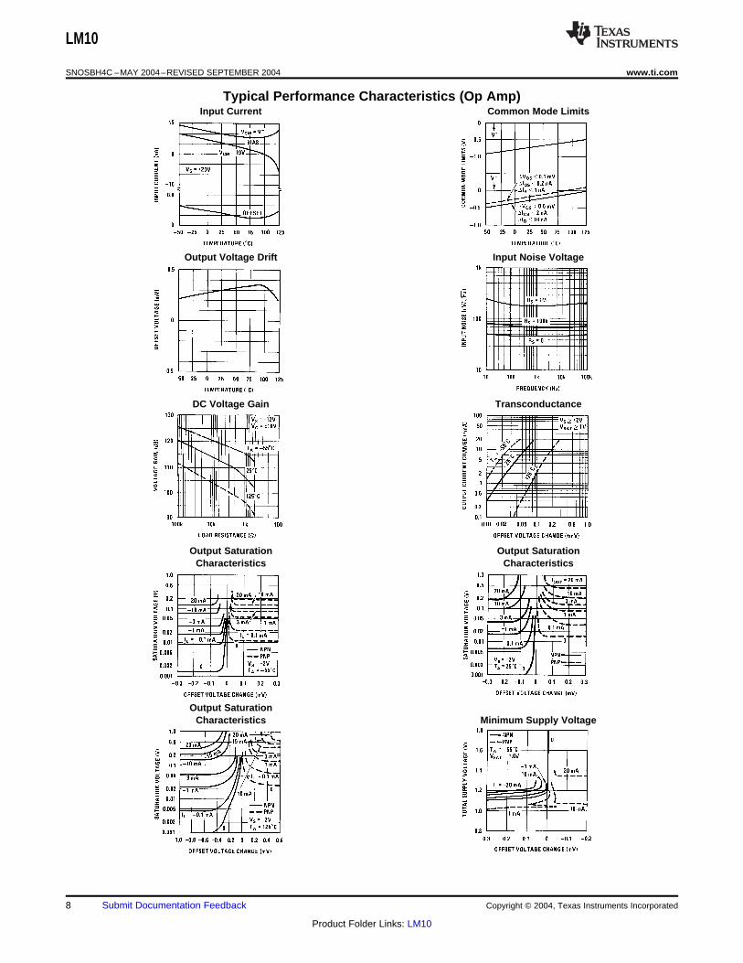
Typical Performance Characteristics (Op Amp)Input Current Common Mode Limits
Output Voltage Drift Input Noise Voltage
DC Voltage Gain Transconductance
Output Saturation Output SaturationCharacteristics Characteristics
Output SaturationCharacteristics Minimum Supply Voltage
8 Submit Documentation Feedback Copyright © 2004, Texas Instruments Incorporated
Product Folder Links: LM10
LM10
www.ti.com SNOSBH4C –MAY 2004–REVISED SEPTEMBER 2004
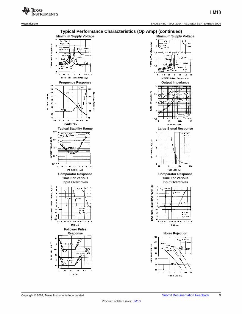
Typical Performance Characteristics (Op Amp) (continued)Minimum Supply Voltage Minimum Supply Voltage
Frequency Response Output Impedance
Typical Stability Range Large Signal Response
Comparator Response Comparator ResponseTime For Various Time For VariousInput Overdrives Input Overdrives
Follower PulseResponse Noise Rejection
Copyright © 2004, Texas Instruments Incorporated Submit Documentation Feedback 9
Product Folder Links: LM10
LM10
SNOSBH4C –MAY 2004–REVISED SEPTEMBER 2004 www.ti.com
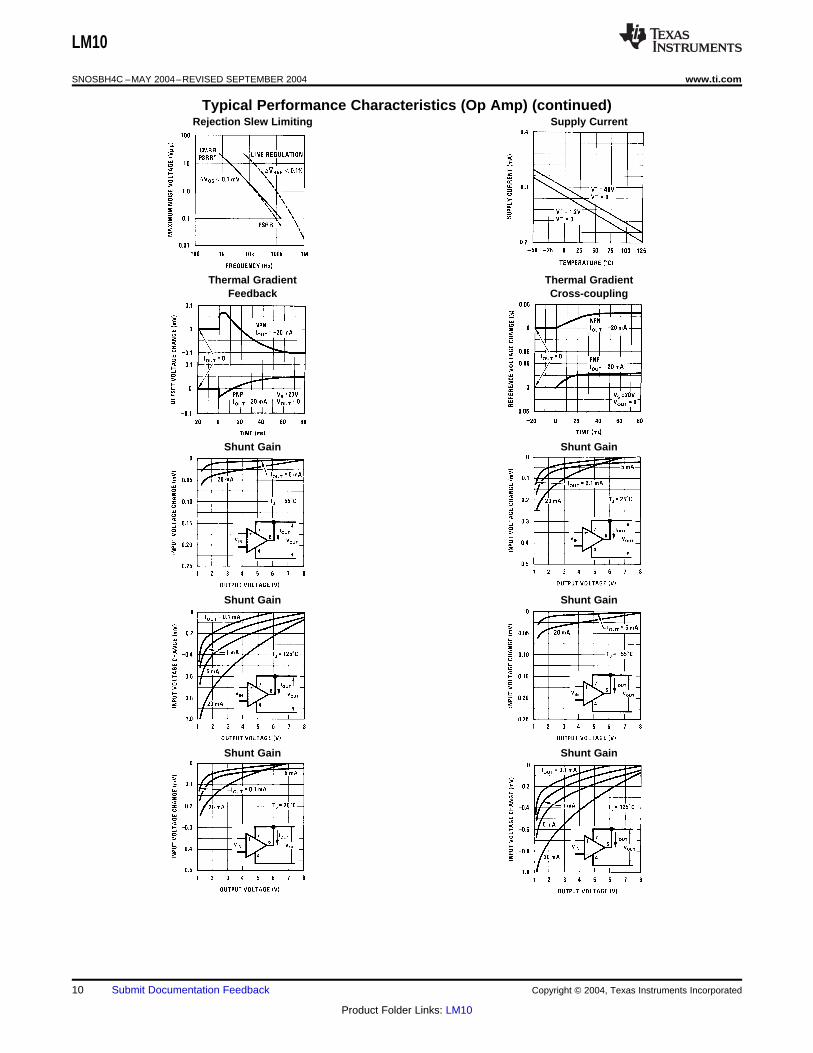
Typical Performance Characteristics (Op Amp) (continued)Rejection Slew Limiting Supply Current
Thermal Gradient Thermal GradientFeedback Cross-coupling
Shunt Gain Shunt Gain
Shunt Gain Shunt Gain
Shunt Gain Shunt Gain
10 Submit Documentation Feedback Copyright © 2004, Texas Instruments Incorporated
Product Folder Links: LM10
LM10
www.ti.com SNOSBH4C –MAY 2004–REVISED SEPTEMBER 2004
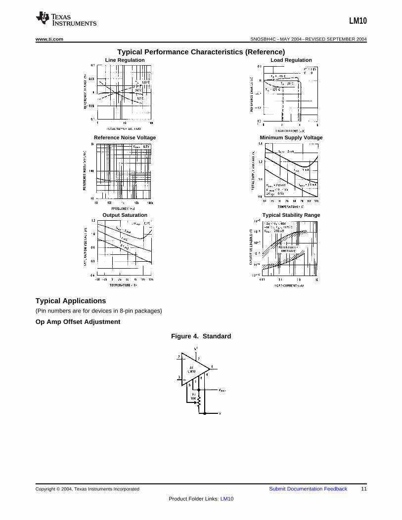
Typical Performance Characteristics (Reference)Line Regulation Load Regulation
Reference Noise Voltage Minimum Supply Voltage
Output Saturation Typical Stability Range
Typical Applications(Pin numbers are for devices in 8-pin packages)
Op Amp Offset Adjustment
Figure 4. Standard
Copyright © 2004, Texas Instruments Incorporated Submit Documentation Feedback 11
Product Folder Links: LM10
LM10
SNOSBH4C –MAY 2004–REVISED SEPTEMBER 2004 www.ti.com
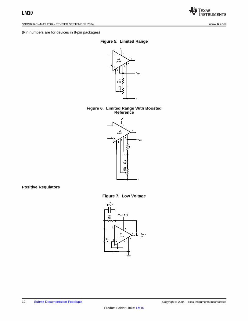
(Pin numbers are for devices in 8-pin packages)
Figure 5. Limited Range
Figure 6. Limited Range With BoostedReference
Positive Regulators
Figure 7. Low Voltage
12 Submit Documentation Feedback Copyright © 2004, Texas Instruments Incorporated
Product Folder Links: LM10
LM10
www.ti.com SNOSBH4C –MAY 2004–REVISED SEPTEMBER 2004
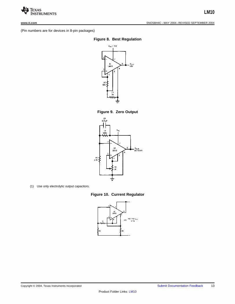
(Pin numbers are for devices in 8-pin packages)
Figure 8. Best Regulation
Figure 9. Zero Output
(1) Use only electrolytic output capacitors.
Figure 10. Current Regulator
Copyright © 2004, Texas Instruments Incorporated Submit Documentation Feedback 13
Product Folder Links: LM10
LM10
SNOSBH4C –MAY 2004–REVISED SEPTEMBER 2004 www.ti.com
(Pin numbers are for devices in 8-pin packages)
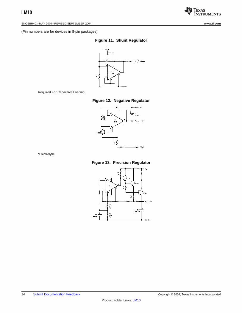
Figure 11. Shunt Regulator
Required For Capacitive Loading
Figure 12. Negative Regulator
*Electrolytic
Figure 13. Precision Regulator
14 Submit Documentation Feedback Copyright © 2004, Texas Instruments Incorporated
Product Folder Links: LM10
LM10
www.ti.com SNOSBH4C –MAY 2004–REVISED SEPTEMBER 2004
(Pin numbers are for devices in 8-pin packages)
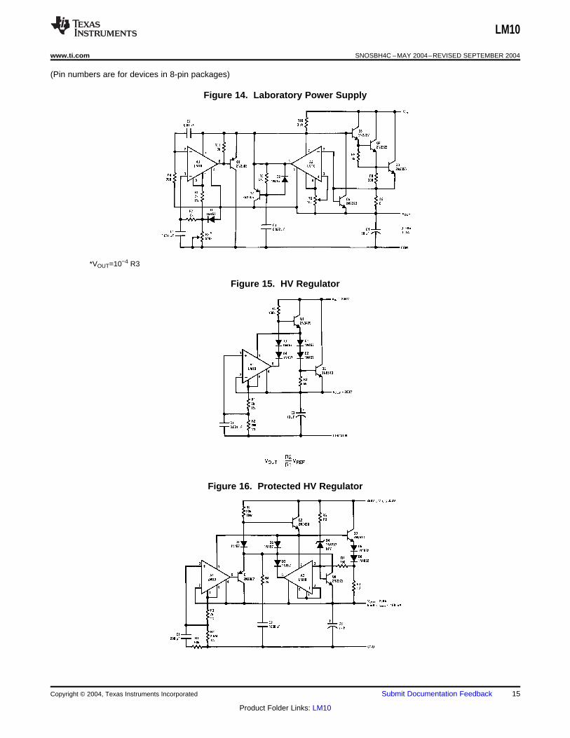
Figure 14. Laboratory Power Supply
*VOUT=10−4 R3
Figure 15. HV Regulator
Figure 16. Protected HV Regulator
Copyright © 2004, Texas Instruments Incorporated Submit Documentation Feedback 15
Product Folder Links: LM10
LM10
SNOSBH4C –MAY 2004–REVISED SEPTEMBER 2004 www.ti.com
(Pin numbers are for devices in 8-pin packages)
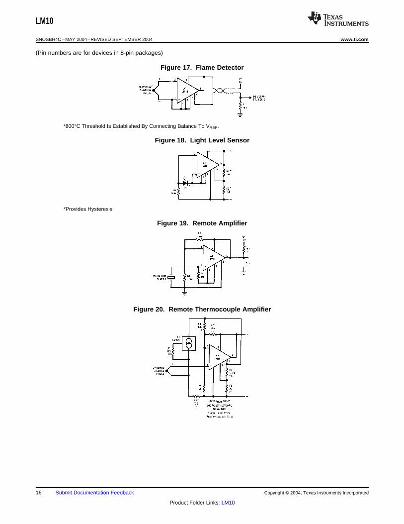
Figure 17. Flame Detector
*800°C Threshold Is Established By Connecting Balance To VREF.
Figure 18. Light Level Sensor
*Provides Hysteresis
Figure 19. Remote Amplifier
Figure 20. Remote Thermocouple Amplifier
16 Submit Documentation Feedback Copyright © 2004, Texas Instruments Incorporated
Product Folder Links: LM10
LM10
www.ti.com SNOSBH4C –MAY 2004–REVISED SEPTEMBER 2004
(Pin numbers are for devices in 8-pin packages)
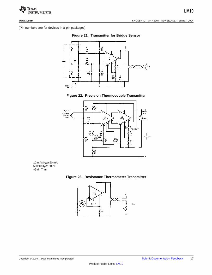
Figure 21. Transmitter for Bridge Sensor
Figure 22. Precision Thermocouple Transmitter
10 mA≤IOUT≤50 mA500°C≤TP≤1500°C*Gain Trim
Figure 23. Resistance Thermometer Transmitter
Copyright © 2004, Texas Instruments Incorporated Submit Documentation Feedback 17
Product Folder Links: LM10
LM10
SNOSBH4C –MAY 2004–REVISED SEPTEMBER 2004 www.ti.com
(Pin numbers are for devices in 8-pin packages)
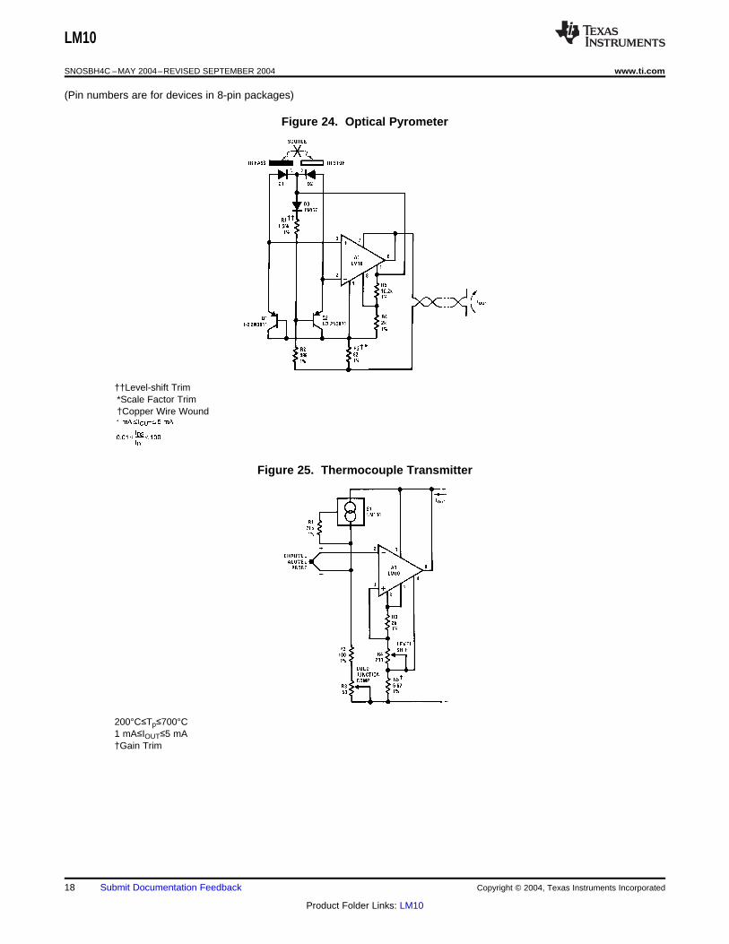
Figure 24. Optical Pyrometer
††Level-shift Trim*Scale Factor Trim†Copper Wire Wound
Figure 25. Thermocouple Transmitter
200°C≤Tp≤700°C1 mA≤IOUT≤5 mA†Gain Trim
18 Submit Documentation Feedback Copyright © 2004, Texas Instruments Incorporated
Product Folder Links: LM10
LM10
www.ti.com SNOSBH4C –MAY 2004–REVISED SEPTEMBER 2004
(Pin numbers are for devices in 8-pin packages)
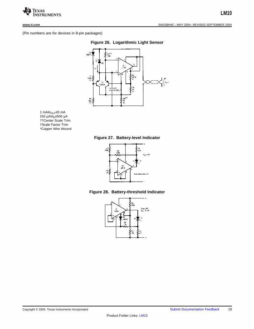
Figure 26. Logarithmic Light Sensor
1 mA≤IOUT≤5 mA‡50 μA≤ID≤500 μA††Center Scale Trim†Scale Factor Trim*Copper Wire Wound
Figure 27. Battery-level Indicator
Figure 28. Battery-threshold Indicator
Copyright © 2004, Texas Instruments Incorporated Submit Documentation Feedback 19
Product Folder Links: LM10
LM10
SNOSBH4C –MAY 2004–REVISED SEPTEMBER 2004 www.ti.com
(Pin numbers are for devices in 8-pin packages)
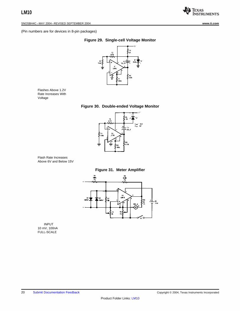
Figure 29. Single-cell Voltage Monitor
Flashes Above 1.2VRate Increases WithVoltage
Figure 30. Double-ended Voltage Monitor
Flash Rate IncreasesAbove 6V and Below 15V
Figure 31. Meter Amplifier
INPUT10 mV, 100nAFULL-SCALE
20 Submit Documentation Feedback Copyright © 2004, Texas Instruments Incorporated
Product Folder Links: LM10
LM10
www.ti.com SNOSBH4C –MAY 2004–REVISED SEPTEMBER 2004
(Pin numbers are for devices in 8-pin packages)
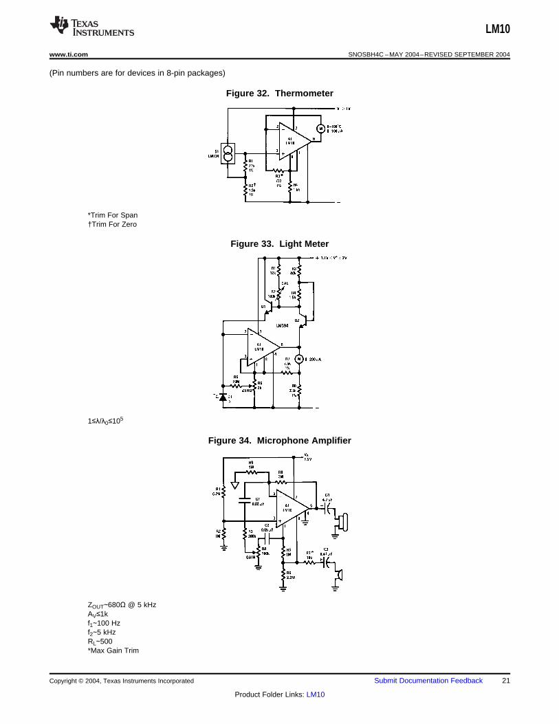
Figure 32. Thermometer
*Trim For Span†Trim For Zero
Figure 33. Light Meter
1≤λ/λ0≤105
Figure 34. Microphone Amplifier
ZOUT∼680Ω @ 5 kHzAV≤1kf1∼100 Hzf2∼5 kHzRL∼500*Max Gain Trim
Copyright © 2004, Texas Instruments Incorporated Submit Documentation Feedback 21
Product Folder Links: LM10
LM10
SNOSBH4C –MAY 2004–REVISED SEPTEMBER 2004 www.ti.com
(Pin numbers are for devices in 8-pin packages)
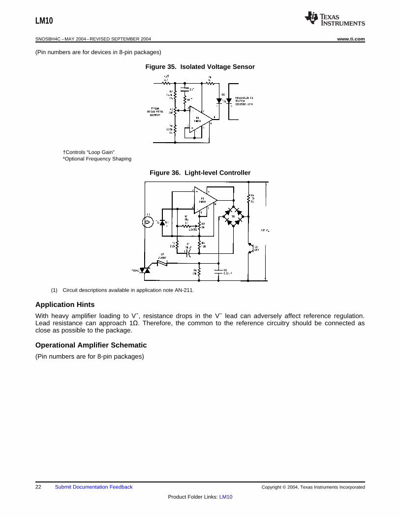
Figure 35. Isolated Voltage Sensor
†Controls “Loop Gain”*Optional Frequency Shaping
Figure 36. Light-level Controller
(1) Circuit descriptions available in application note AN-211.
Application Hints
With heavy amplifier loading to V−, resistance drops in the V− lead can adversely affect reference regulation.Lead resistance can approach 1Ω. Therefore, the common to the reference circuitry should be connected asclose as possible to the package.
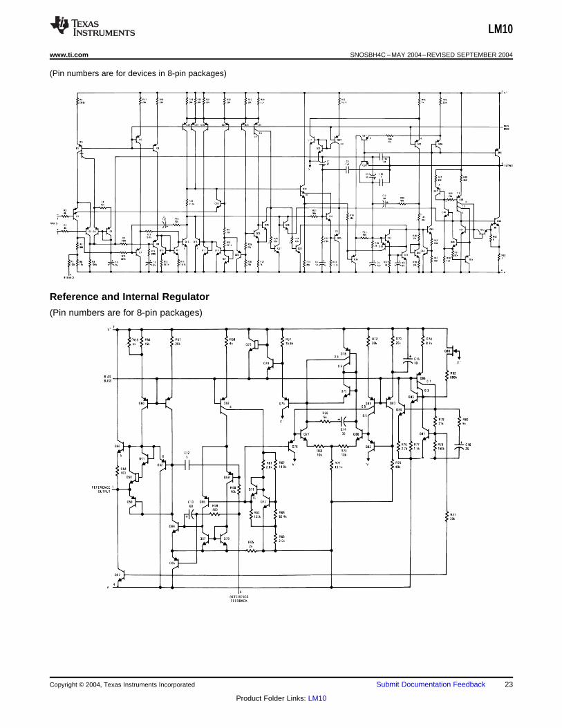
Operational Amplifier Schematic
(Pin numbers are for 8-pin packages)
22 Submit Documentation Feedback Copyright © 2004, Texas Instruments Incorporated
Product Folder Links: LM10
LM10
www.ti.com SNOSBH4C –MAY 2004–REVISED SEPTEMBER 2004
(Pin numbers are for devices in 8-pin packages)
Reference and Internal Regulator
(Pin numbers are for 8-pin packages)
Copyright © 2004, Texas Instruments Incorporated Submit Documentation Feedback 23
Product Folder Links: LM10
PACKAGE OPTION ADDENDUM
www.ti.com 17-Nov-2012
Addendum-Page 1
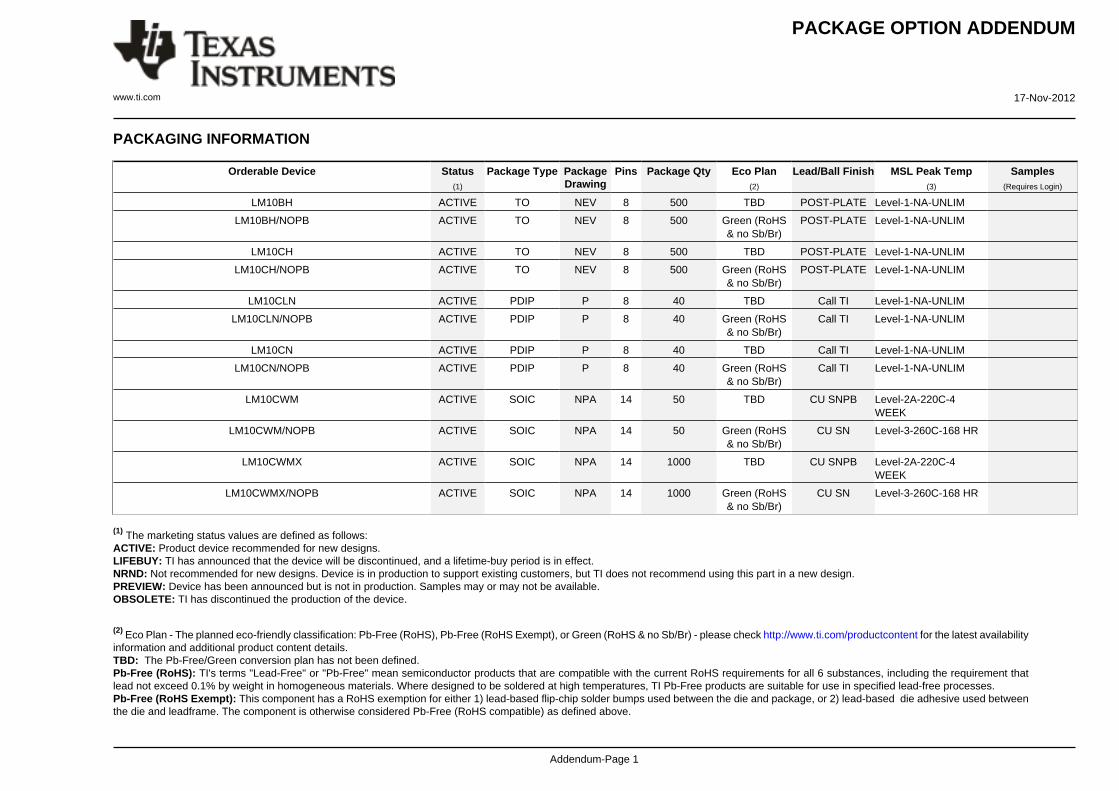
PACKAGING INFORMATION
Orderable Device Status(1)
Package Type PackageDrawing
Pins Package Qty Eco Plan(2)
Lead/Ball Finish MSL Peak Temp(3)
Samples(Requires Login)
LM10BH ACTIVE TO NEV 8 500 TBD POST-PLATE Level-1-NA-UNLIM
LM10BH/NOPB ACTIVE TO NEV 8 500 Green (RoHS& no Sb/Br)
POST-PLATE Level-1-NA-UNLIM
LM10CH ACTIVE TO NEV 8 500 TBD POST-PLATE Level-1-NA-UNLIM
LM10CH/NOPB ACTIVE TO NEV 8 500 Green (RoHS& no Sb/Br)
POST-PLATE Level-1-NA-UNLIM
LM10CLN ACTIVE PDIP P 8 40 TBD Call TI Level-1-NA-UNLIM
LM10CLN/NOPB ACTIVE PDIP P 8 40 Green (RoHS& no Sb/Br)
Call TI Level-1-NA-UNLIM
LM10CN ACTIVE PDIP P 8 40 TBD Call TI Level-1-NA-UNLIM
LM10CN/NOPB ACTIVE PDIP P 8 40 Green (RoHS& no Sb/Br)
Call TI Level-1-NA-UNLIM
LM10CWM ACTIVE SOIC NPA 14 50 TBD CU SNPB Level-2A-220C-4WEEK
LM10CWM/NOPB ACTIVE SOIC NPA 14 50 Green (RoHS& no Sb/Br)
CU SN Level-3-260C-168 HR
LM10CWMX ACTIVE SOIC NPA 14 1000 TBD CU SNPB Level-2A-220C-4WEEK
LM10CWMX/NOPB ACTIVE SOIC NPA 14 1000 Green (RoHS& no Sb/Br)
CU SN Level-3-260C-168 HR
(1) The marketing status values are defined as follows:ACTIVE: Product device recommended for new designs.LIFEBUY: TI has announced that the device will be discontinued, and a lifetime-buy period is in effect.NRND: Not recommended for new designs. Device is in production to support existing customers, but TI does not recommend using this part in a new design.PREVIEW: Device has been announced but is not in production. Samples may or may not be available.OBSOLETE: TI has discontinued the production of the device.
(2) Eco Plan - The planned eco-friendly classification: Pb-Free (RoHS), Pb-Free (RoHS Exempt), or Green (RoHS & no Sb/Br) - please check http://www.ti.com/productcontent for the latest availabilityinformation and additional product content details.TBD: The Pb-Free/Green conversion plan has not been defined.Pb-Free (RoHS): TI's terms "Lead-Free" or "Pb-Free" mean semiconductor products that are compatible with the current RoHS requirements for all 6 substances, including the requirement thatlead not exceed 0.1% by weight in homogeneous materials. Where designed to be soldered at high temperatures, TI Pb-Free products are suitable for use in specified lead-free processes.Pb-Free (RoHS Exempt): This component has a RoHS exemption for either 1) lead-based flip-chip solder bumps used between the die and package, or 2) lead-based die adhesive used betweenthe die and leadframe. The component is otherwise considered Pb-Free (RoHS compatible) as defined above.
PACKAGE OPTION ADDENDUM
www.ti.com 17-Nov-2012
Addendum-Page 2
Green (RoHS & no Sb/Br): TI defines "Green" to mean Pb-Free (RoHS compatible), and free of Bromine (Br) and Antimony (Sb) based flame retardants (Br or Sb do not exceed 0.1% by weightin homogeneous material)
(3) MSL, Peak Temp. -- The Moisture Sensitivity Level rating according to the JEDEC industry standard classifications, and peak solder temperature.
Important Information and Disclaimer:The information provided on this page represents TI's knowledge and belief as of the date that it is provided. TI bases its knowledge and belief on informationprovided by third parties, and makes no representation or warranty as to the accuracy of such information. Efforts are underway to better integrate information from third parties. TI has taken andcontinues to take reasonable steps to provide representative and accurate information but may not have conducted destructive testing or chemical analysis on incoming materials and chemicals.TI and TI suppliers consider certain information to be proprietary, and thus CAS numbers and other limited information may not be available for release.
In no event shall TI's liability arising out of such information exceed the total purchase price of the TI part(s) at issue in this document sold by TI to Customer on an annual basis.
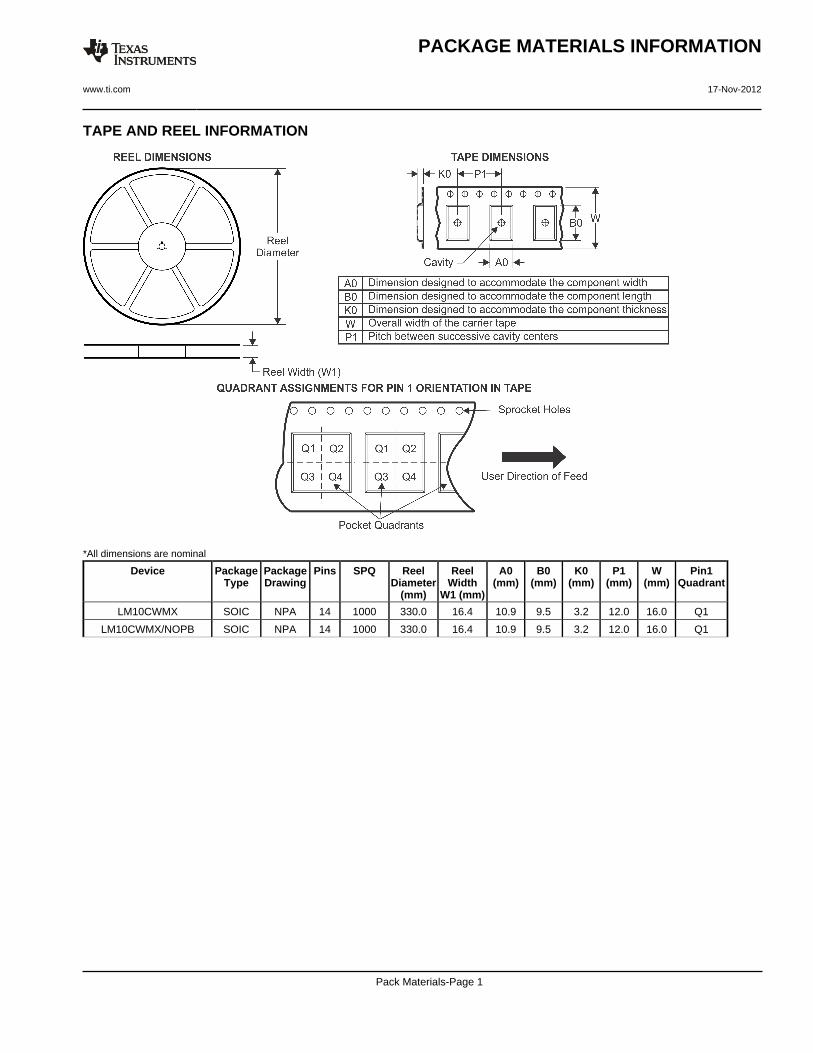
TAPE AND REEL INFORMATION
*All dimensions are nominal
Device PackageType
PackageDrawing
Pins SPQ ReelDiameter
(mm)
ReelWidth
W1 (mm)
A0(mm)
B0(mm)
K0(mm)
P1(mm)
W(mm)
Pin1Quadrant
LM10CWMX SOIC NPA 14 1000 330.0 16.4 10.9 9.5 3.2 12.0 16.0 Q1
LM10CWMX/NOPB SOIC NPA 14 1000 330.0 16.4 10.9 9.5 3.2 12.0 16.0 Q1
PACKAGE MATERIALS INFORMATION
www.ti.com 17-Nov-2012
Pack Materials-Page 1
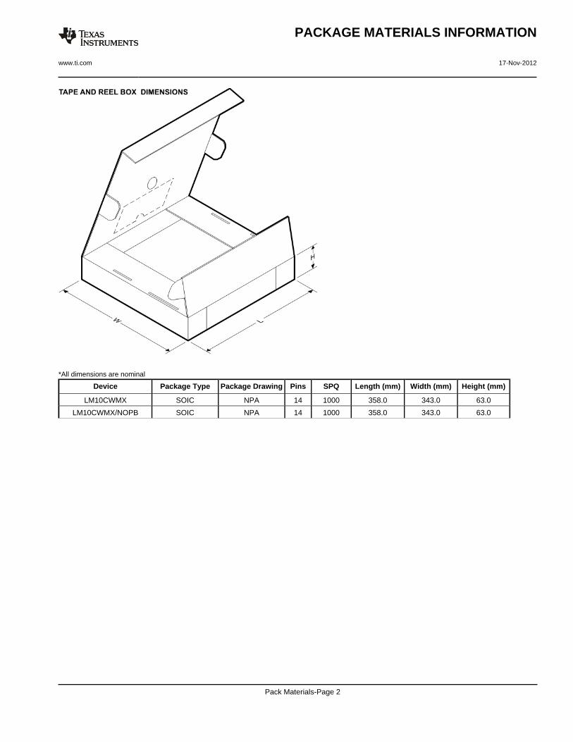
*All dimensions are nominal
Device Package Type Package Drawing Pins SPQ Length (mm) Width (mm) Height (mm)
LM10CWMX SOIC NPA 14 1000 358.0 343.0 63.0
LM10CWMX/NOPB SOIC NPA 14 1000 358.0 343.0 63.0
PACKAGE MATERIALS INFORMATION
www.ti.com 17-Nov-2012
Pack Materials-Page 2

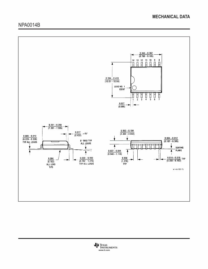
MECHANICAL DATA
NPA0014B
www.ti.com
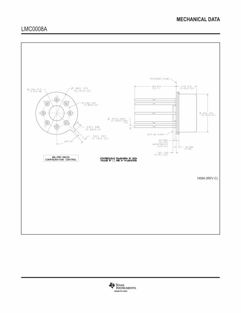
MECHANICAL DATA
LMC0008A
www.ti.com
H08A (REV C)
a0412025
Text Box
NEV0008A
IMPORTANT NOTICE
Texas Instruments Incorporated and its subsidiaries (TI) reserve the right to make corrections, enhancements, improvements and otherchanges to its semiconductor products and services per JESD46, latest issue, and to discontinue any product or service per JESD48, latestissue. Buyers should obtain the latest relevant information before placing orders and should verify that such information is current andcomplete. All semiconductor products (also referred to herein as “components”) are sold subject to TI’s terms and conditions of salesupplied at the time of order acknowledgment.
TI warrants performance of its components to the specifications applicable at the time of sale, in accordance with the warranty in TI’s termsand conditions of sale of semiconductor products. Testing and other quality control techniques are used to the extent TI deems necessaryto support this warranty. Except where mandated by applicable law, testing of all parameters of each component is not necessarilyperformed.
TI assumes no liability for applications assistance or the design of Buyers’ products. Buyers are responsible for their products andapplications using TI components. To minimize the risks associated with Buyers’ products and applications, Buyers should provideadequate design and operating safeguards.
TI does not warrant or represent that any license, either express or implied, is granted under any patent right, copyright, mask work right, orother intellectual property right relating to any combination, machine, or process in which TI components or services are used. Informationpublished by TI regarding third-party products or services does not constitute a license to use such products or services or a warranty orendorsement thereof. Use of such information may require a license from a third party under the patents or other intellectual property of thethird party, or a license from TI under the patents or other intellectual property of TI.
Reproduction of significant portions of TI information in TI data books or data sheets is permissible only if reproduction is without alterationand is accompanied by all associated warranties, conditions, limitations, and notices. TI is not responsible or liable for such altereddocumentation. Information of third parties may be subject to additional restrictions.
Resale of TI components or services with statements different from or beyond the parameters stated by TI for that component or servicevoids all express and any implied warranties for the associated TI component or service and is an unfair and deceptive business practice.TI is not responsible or liable for any such statements.
Buyer acknowledges and agrees that it is solely responsible for compliance with all legal, regulatory and safety-related requirementsconcerning its products, and any use of TI components in its applications, notwithstanding any applications-related information or supportthat may be provided by TI. Buyer represents and agrees that it has all the necessary expertise to create and implement safeguards whichanticipate dangerous consequences of failures, monitor failures and their consequences, lessen the likelihood of failures that might causeharm and take appropriate remedial actions. Buyer will fully indemnify TI and its representatives against any damages arising out of the useof any TI components in safety-critical applications.
In some cases, TI components may be promoted specifically to facilitate safety-related applications. With such components, TI’s goal is tohelp enable customers to design and create their own end-product solutions that meet applicable functional safety standards andrequirements. Nonetheless, such components are subject to these terms.
No TI components are authorized for use in FDA Class III (or similar life-critical medical equipment) unless authorized officers of the partieshave executed a special agreement specifically governing such use.
Only those TI components which TI has specifically designated as military grade or “enhanced plastic” are designed and intended for use inmilitary/aerospace applications or environments. Buyer acknowledges and agrees that any military or aerospace use of TI componentswhich have not been so designated is solely at the Buyer's risk, and that Buyer is solely responsible for compliance with all legal andregulatory requirements in connection with such use.
TI has specifically designated certain components as meeting ISO/TS16949 requirements, mainly for automotive use. In any case of use ofnon-designated products, TI will not be responsible for any failure to meet ISO/TS16949.
Products Applications
Audio www.ti.com/audio Automotive and Transportation www.ti.com/automotive
Amplifiers amplifier.ti.com Communications and Telecom www.ti.com/communications
Data Converters dataconverter.ti.com Computers and Peripherals www.ti.com/computers
DLP® Products www.dlp.com Consumer Electronics www.ti.com/consumer-apps
DSP dsp.ti.com Energy and Lighting www.ti.com/energy
Clocks and Timers www.ti.com/clocks Industrial www.ti.com/industrial
Interface interface.ti.com Medical www.ti.com/medical
Logic logic.ti.com Security www.ti.com/security
Power Mgmt power.ti.com Space, Avionics and Defense www.ti.com/space-avionics-defense
Microcontrollers microcontroller.ti.com Video and Imaging www.ti.com/video
RFID www.ti-rfid.com
OMAP Applications Processors www.ti.com/omap TI E2E Community e2e.ti.com
Wireless Connectivity www.ti.com/wirelessconnectivity
Mailing Address: Texas Instruments, Post Office Box 655303, Dallas, Texas 75265Copyright © 2012, Texas Instruments Incorporated
Mouser Electronics
Authorized Distributor
Click to View Pricing, Inventory, Delivery & Lifecycle Information: Texas Instruments:
LM10BH LM10BH/NOPB LM10CH LM10CH/NOPB LM10CLN LM10CLN/NOPB LM10CN LM10CN/NOPB
LM10CWM LM10CWM/NOPB LM10CWMX LM10CWMX/NOPB


![Filter Design with Op-amptera.yonsei.ac.kr/class/2020_1_1/lecture/Lect 29 Project... · 2020. 7. 8. · • Filter Design with ideal Op-amp [10], Operational Amplifier [20] ,Filter](https://static.fdocument.org/doc/165x107/60a6ee382a29926a6905df36/filter-design-with-op-29-project-2020-7-8-a-filter-design-with-ideal.jpg)