TOSHIBA CMOS Integrated Circuit Silicon Monolithic TC78B025FTG
© PSU
Summer Course: Summer Course: Advanced Topics in Modern VLSI designAdvanced Topics in Modern VLSI design
Instructor: Yuan [email protected]
http://www.cse.psu.edu/~yuanxieCourse website:
http://www.cse.psu.edu/~yuanxie/Tsinghua/
Lecture 4: 3D Integrated Circuit Design
© PSU2现代VLSI设计技术 Lecture 04, 谢源,2006/8
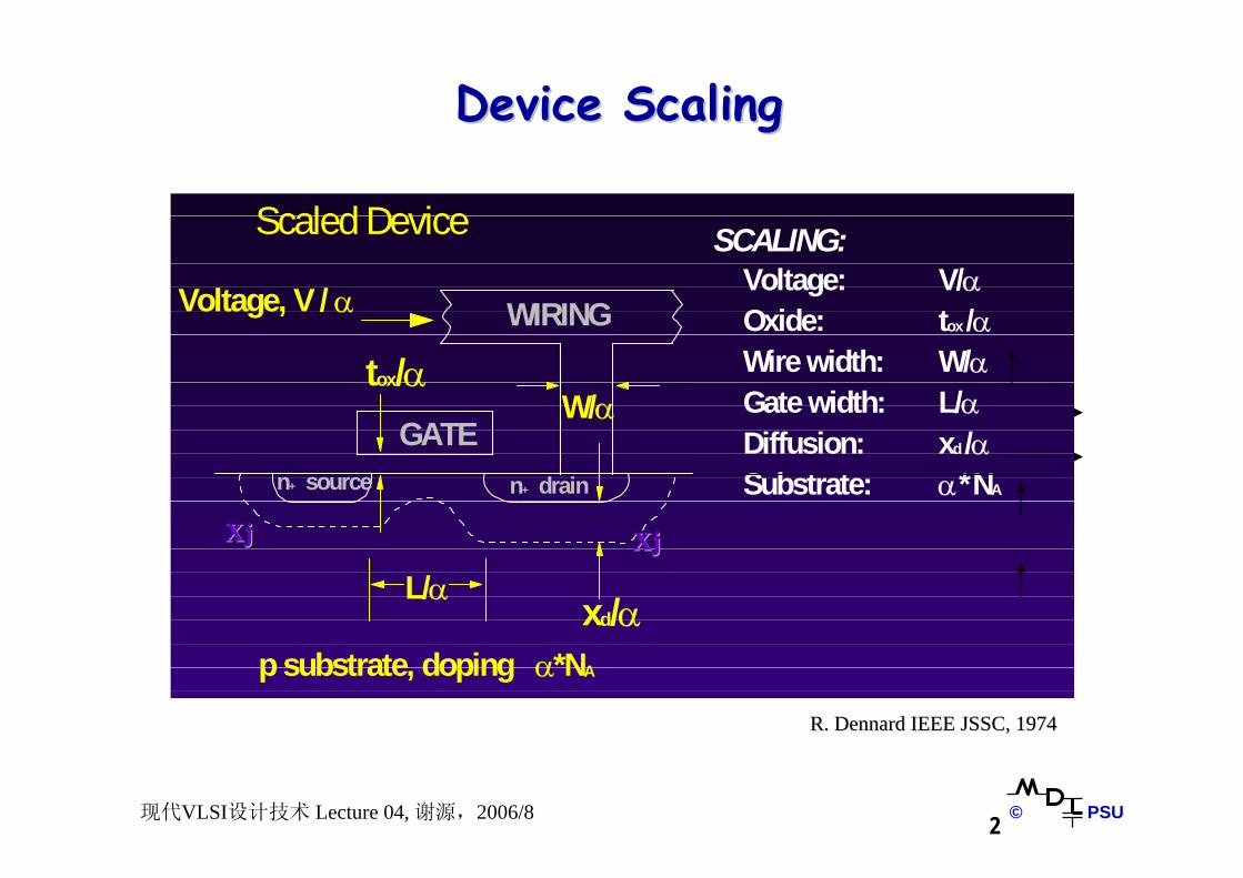
Device Scaling Device Scaling
SCALING:Voltage: V/αOxide: tox /αWire width: W/αGate width: L/αDiffusion: xd /αSubstrate: α * NA
Scaled Device
L/α xd/α
GATEn+ source n+ drain
WIRINGVoltage, V / α
W/α
p substrate, doping α*NA
tox/α
R. Dennard IEEE JSSC, 1974R. Dennard IEEE JSSC, 1974
XjXj XjXj
© PSU3现代VLSI设计技术 Lecture 04, 谢源,2006/8
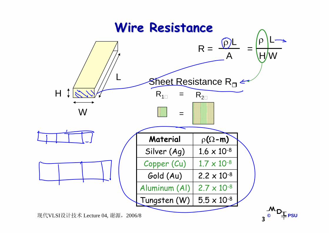
Wire ResistanceWire Resistance
L
W
H
R =ρ L
H W
Sheet Resistance RR1 R2=
=
ρ LA
=
5.5 x 10⁻⁸Tungsten (W)2.7 x 10⁻⁸Aluminum (Al)2.2 x 10⁻⁸Gold (Au)1.7 x 10⁻⁸Copper (Cu)1.6 x 10⁻⁸Silver (Ag)ρ(Ω-m)Material
© PSU4现代VLSI设计技术 Lecture 04, 谢源,2006/8
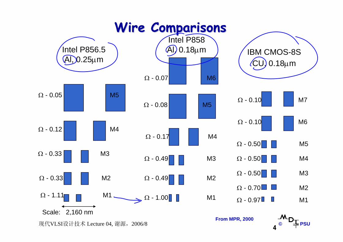
Wire ComparisonsWire ComparisonsIntel P856.5Al, 0.25µm
Ω - 0.33 M2
Ω - 0.33 M3
Ω - 0.12 M4
Ω - 1.11 M1
Ω - 0.05 M5
Scale: 2,160 nm
Ω - 0.49 M2
Ω - 0.49 M3
Ω - 0.17 M4
Ω - 1.00 M1
Ω - 0.08 M5
Ω - 0.07 M6
Intel P858Al, 0.18µm IBM CMOS-8S
CU, 0.18µm
Ω - 0.97 M1
Ω - 0.10 M6
Ω - 0.10 M7
Ω - 0.70 M2
Ω - 0.50 M3
Ω - 0.50 M4
Ω - 0.50 M5
From MPR, 2000
© PSU5现代VLSI设计技术 Lecture 04, 谢源,2006/8
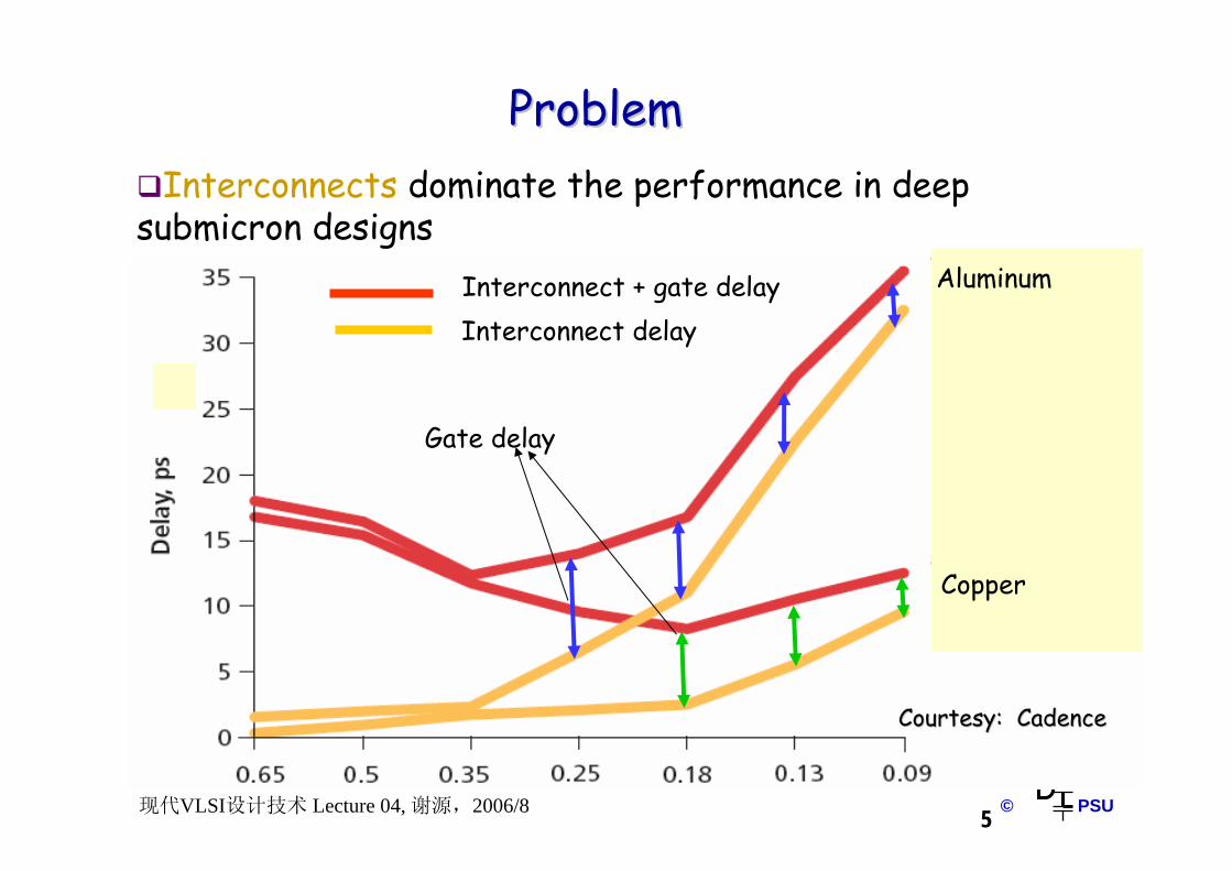
ProblemProblem
Courtesy: CadenceCourtesy: Cadence
Interconnects dominate the performance in deep submicron designs
Interconnect + gate delayInterconnect delay
Aluminum
Copper
Gate delay
© PSU7现代VLSI设计技术 Lecture 04, 谢源,2006/8
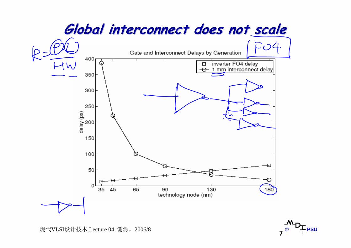
Global interconnect does not scaleGlobal interconnect does not scale
© PSU8现代VLSI设计技术 Lecture 04, 谢源,2006/8
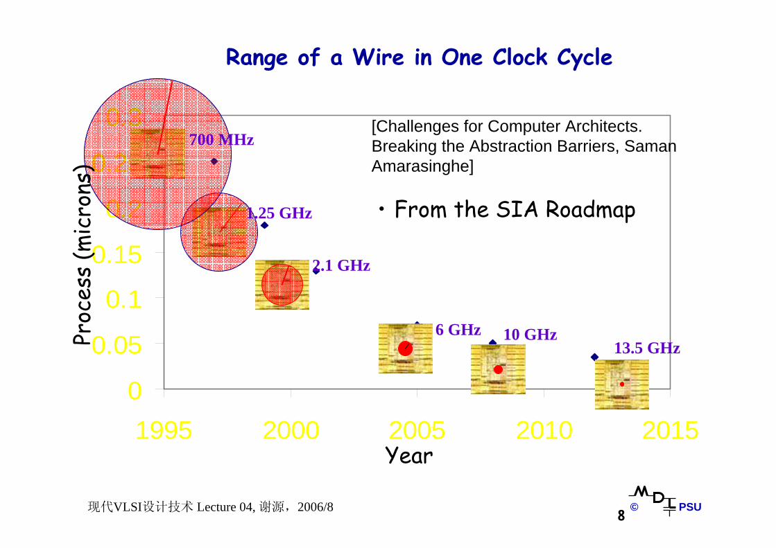
Range of a Wire in One Clock Cycle
0
0.05
0.1
0.15
0.2
0.25
0.3
1995 2000 2005 2010 2015Year
Proc
ess
(mic
rons
)
700 MHz
1.25 GHz
2.1 GHz
6 GHz 10 GHz13.5 GHz
• From the SIA Roadmap
[Challenges for Computer Architects. Breaking the Abstraction Barriers, SamanAmarasinghe]
© PSU9现代VLSI设计技术 Lecture 04, 谢源,2006/8
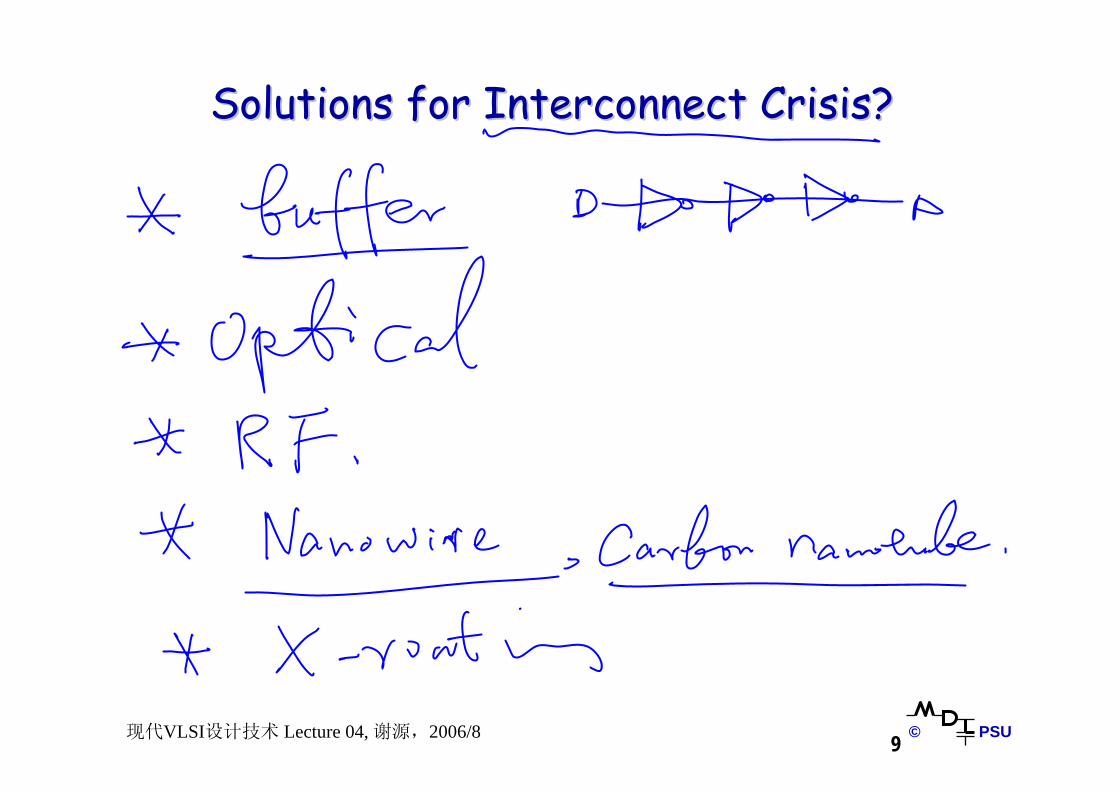
Solutions for Interconnect Crisis?Solutions for Interconnect Crisis?
© PSU10现代VLSI设计技术 Lecture 04, 谢源,2006/8
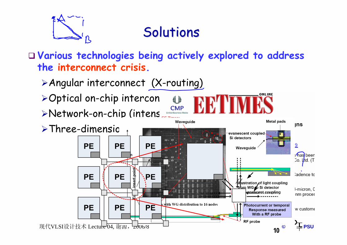
SolutionsSolutionsVarious technologies being actively explored to address the interconnect crisis.
Angular interconnect (X-routing)Optical on-chip interconnect Network-on-chip (intensive research since 2000)Three-dimensional (3D) Integration
© PSU11现代VLSI设计技术 Lecture 04, 谢源,2006/8
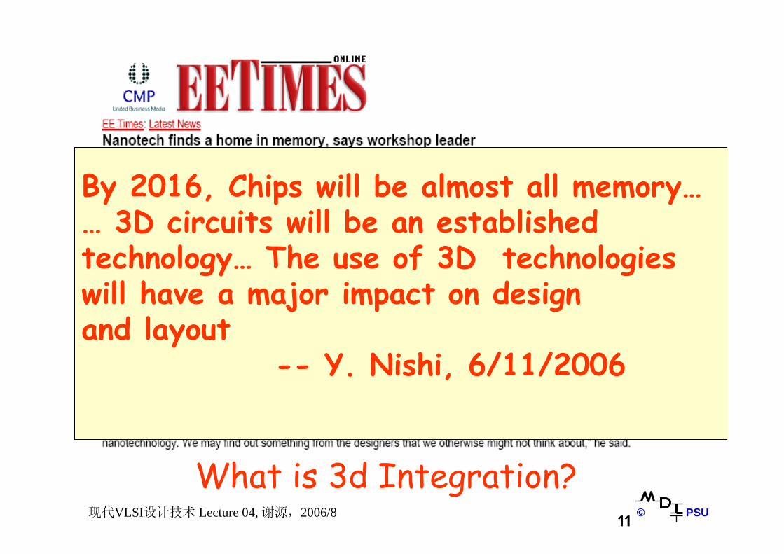
What is 3d Integration?
By 2016, Chips will be almost all memory…… 3D circuits will be an established technology… The use of 3D technologies will have a major impact on design and layout
-- Y. Nishi, 6/11/2006
© PSU12现代VLSI设计技术 Lecture 04, 谢源,2006/8
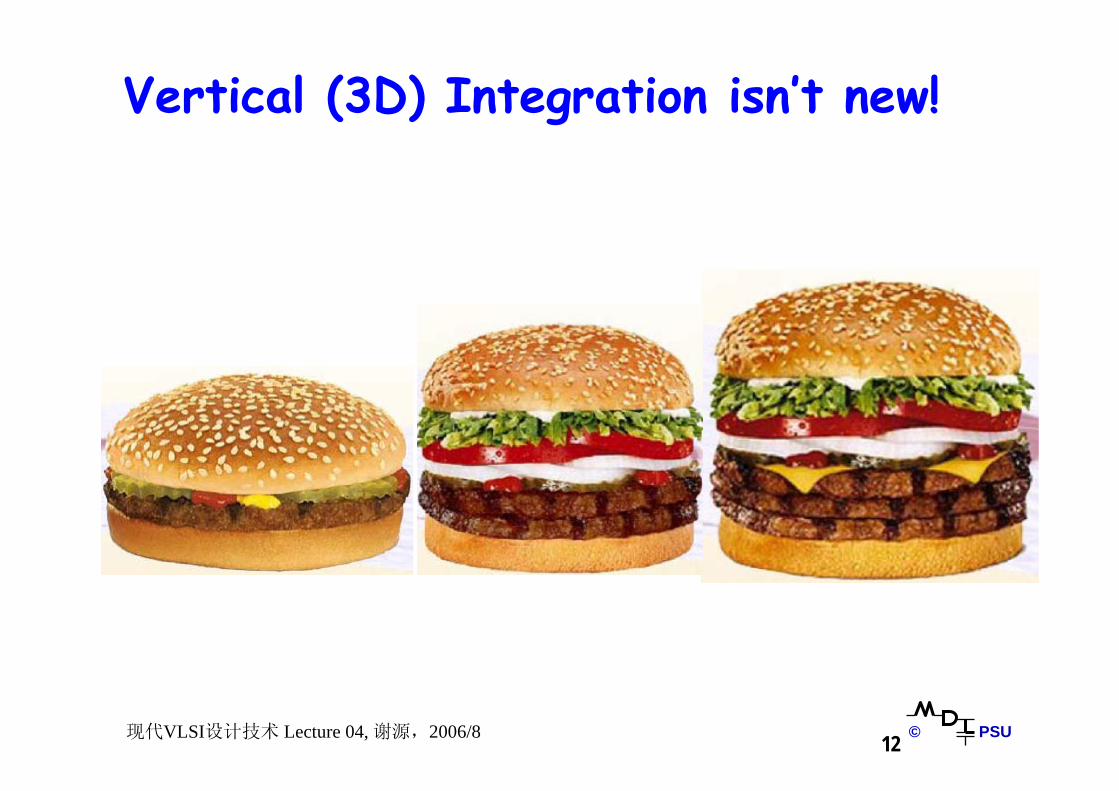
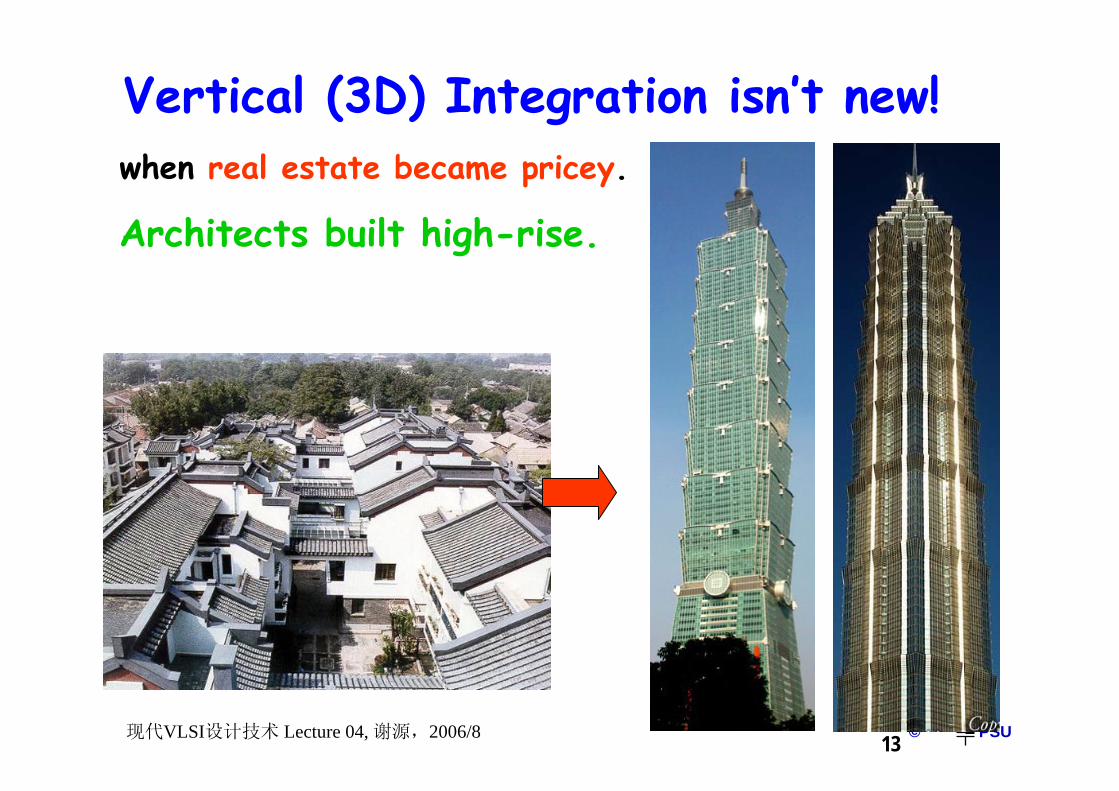
Vertical (3D) Integration isn’t new!
© PSU13现代VLSI设计技术 Lecture 04, 谢源,2006/8
Vertical (3D) Integration isn’t new! when real estate became pricey.
Architects built high-rise.
© PSU14现代VLSI设计技术 Lecture 04, 谢源,2006/8
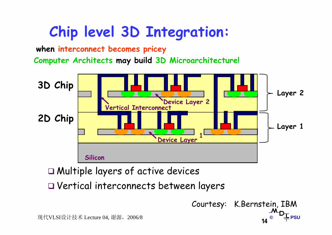
Device Layer 2Vertical Interconnect
Silicon
1
Multiple layers of active devicesVertical interconnects between layers
Device Layer
Silicon
1
Courtesy: K.Bernstein, IBM
2D Chip
3D Chip
Chip level 3D Integration:
Layer 1
Layer 2
when interconnect becomes priceyComputer Architects may build 3D Microarchitecture!
© PSU15现代VLSI设计技术 Lecture 04, 谢源,2006/8
Benefits of ThreeBenefits of Three--Dimensional Chip ?Dimensional Chip ?
© PSU16现代VLSI设计技术 Lecture 04, 谢源,2006/8
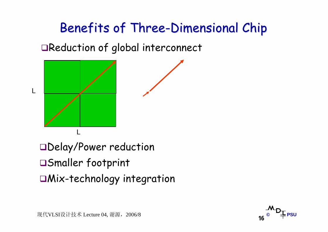
Benefits of ThreeBenefits of Three--Dimensional ChipDimensional ChipReduction of global interconnect
L
L
Delay/Power reductionSmaller footprintMix-technology integration
© PSU17现代VLSI设计技术 Lecture 04, 谢源,2006/8
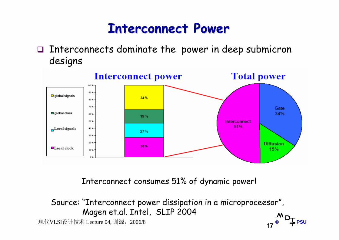
Interconnect PowerInterconnect PowerInterconnects dominate the power in deep submicron designs
Interconnect consumes 51% of dynamic power!
Source: “Interconnect power dissipation in a microproceesor”,Magen et.al. Intel, SLIP 2004
© PSU18现代VLSI设计技术 Lecture 04, 谢源,2006/8
How to build 3D Chip: wafer bondingHow to build 3D Chip: wafer bonding
Bulk Si
Burried Si
Burried Si
Bulk Si
Bulk Si
Bulk Si
metal & ILD layers 1active device layer 1
active device layer 2
active device layer 3
Burried Si
Burried Simetal & ILD layers 2
metal & ILD layers 3
Face-to-Back Wafer-Bonding
3D Via0.2μm x 0.2μm ~
10μm x 10μm
IBM Nov. 2002
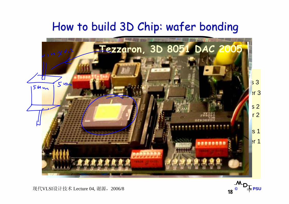
Tezzaron, 3D 8051 DAC 2005
© PSU19现代VLSI设计技术 Lecture 04, 谢源,2006/8
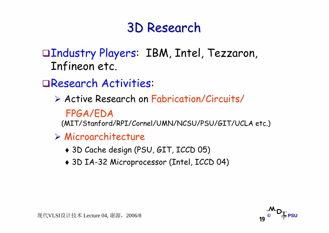
3D Research3D Research
Industry Players: IBM, Intel, Tezzaron, Infineon etc.Research Activities:
Active Research on Fabrication/Circuits/FPGA/EDA
(MIT/Stanford/RPI/Cornel/UMN/NCSU/PSU/GIT/UCLA etc.)
Microarchitecture3D Cache design (PSU, GIT, ICCD 05) 3D IA-32 Microprocessor (Intel, ICCD 04)
© PSU20现代VLSI设计技术 Lecture 04, 谢源,2006/8
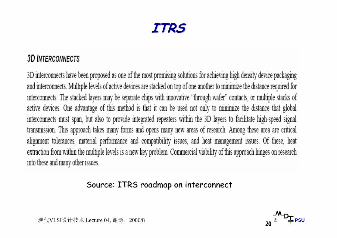
ITRSITRS
Source: ITRS roadmap on interconnectSource: ITRS roadmap on interconnect
© PSU21现代VLSI设计技术 Lecture 04, 谢源,2006/8
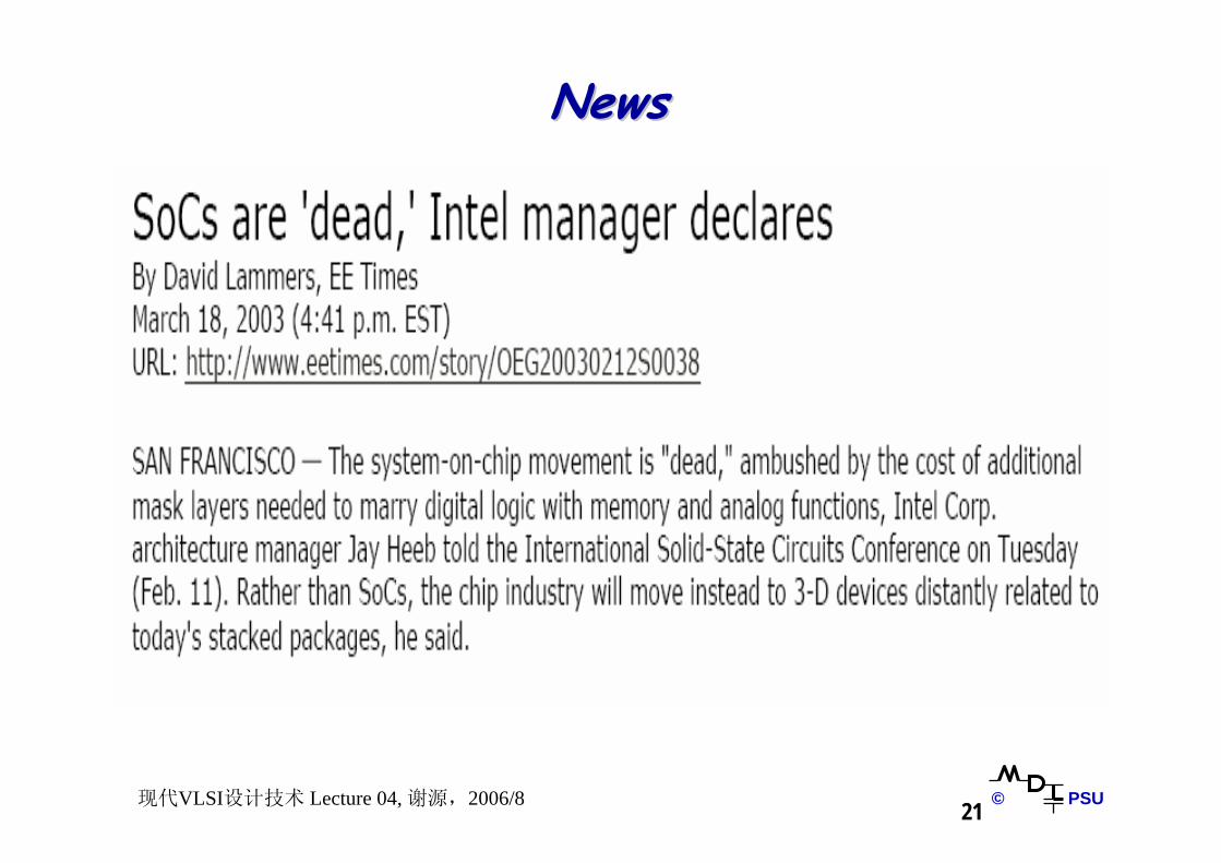
NewsNews
Source: ITRS roadmap on interconnectSource: ITRS roadmap on interconnect
© PSU22现代VLSI设计技术 Lecture 04, 谢源,2006/8
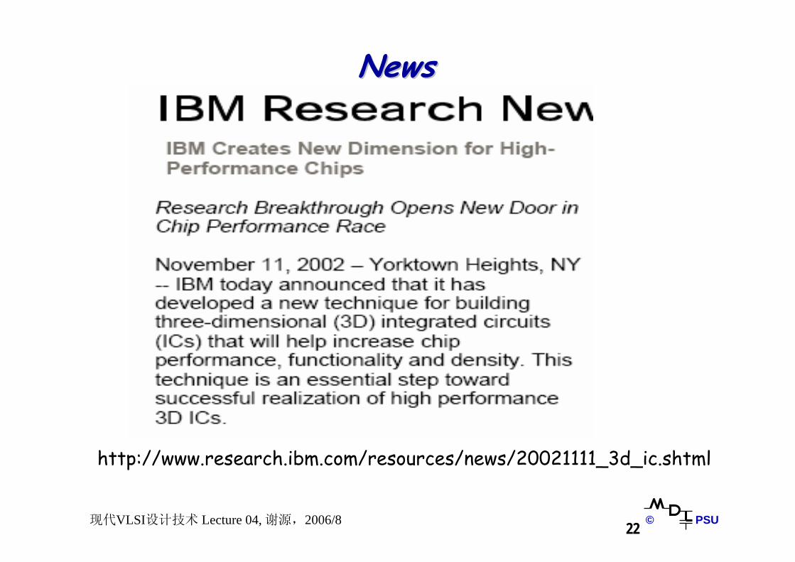
NewsNews
http://www.research.ibm.com/resources/news/20021111_3d_ic.shtml
© PSU23现代VLSI设计技术 Lecture 04, 谢源,2006/8
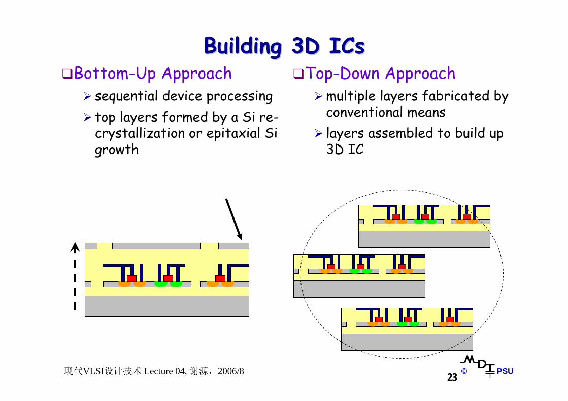
Building 3D ICsBuilding 3D ICsBottom-Up Approach
sequential device processingtop layers formed by a Si re-crystallization or epitaxial Sigrowth
Top-Down Approachmultiple layers fabricated by conventional meanslayers assembled to build up 3D IC
© PSU24现代VLSI设计技术 Lecture 04, 谢源,2006/8
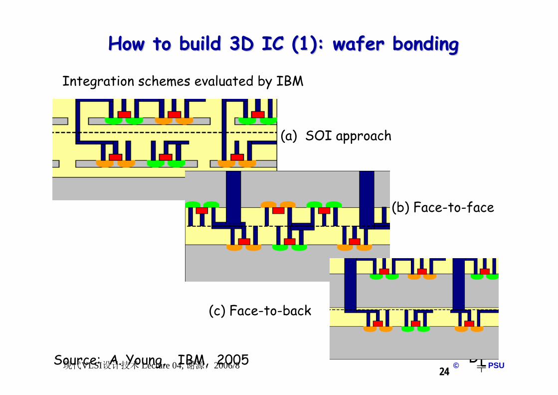
How to build 3D IC (1): wafer bonding How to build 3D IC (1): wafer bonding
(a) SOI approach
(b) Face-to-face
(c) Face-to-back
Integration schemes evaluated by IBM
Source: A. Young, IBM, 2005
© PSU25现代VLSI设计技术 Lecture 04, 谢源,2006/8
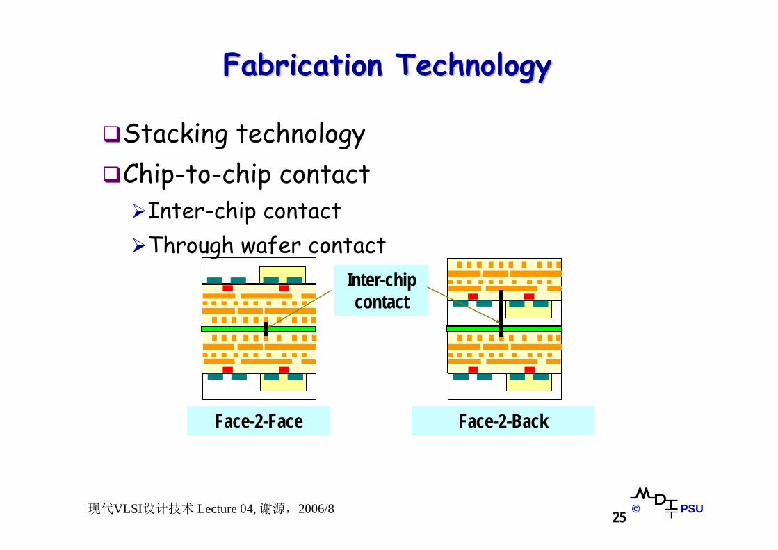
Fabrication TechnologyFabrication Technology
Stacking technologyChip-to-chip contact
Inter-chip contactThrough wafer contact
Face-2-Face Face-2-Back
Inter-chip contact
© PSU26现代VLSI设计技术 Lecture 04, 谢源,2006/8
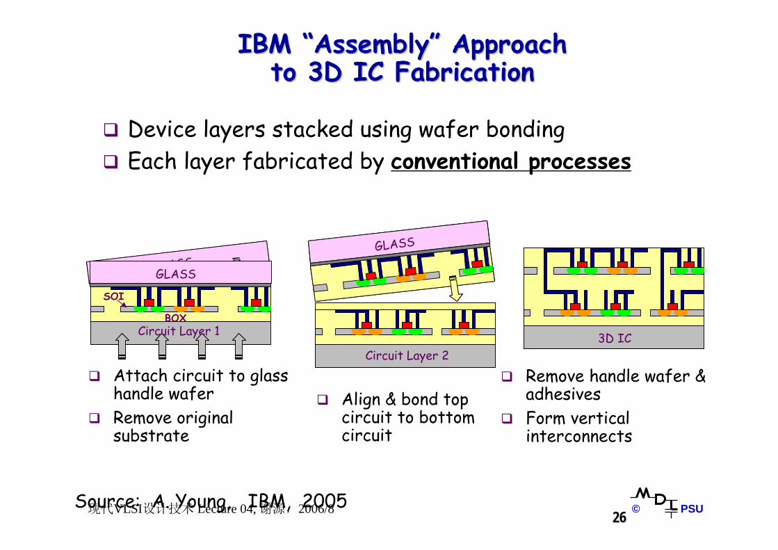
IBM IBM ““AssemblyAssembly”” Approach Approach to 3D IC Fabricationto 3D IC Fabrication
Device layers stacked using wafer bondingEach layer fabricated by conventional processes
GLASSGLASS
Circuit Layer 1
Circuit Layer 23D IC
GLASS
Attach circuit to glass handle waferRemove original substrate
Align & bond top circuit to bottom circuit
Remove handle wafer & adhesivesForm vertical interconnects
BOX
SOI
Source: A. Young, IBM, 2005
© PSU27现代VLSI设计技术 Lecture 04, 谢源,2006/8
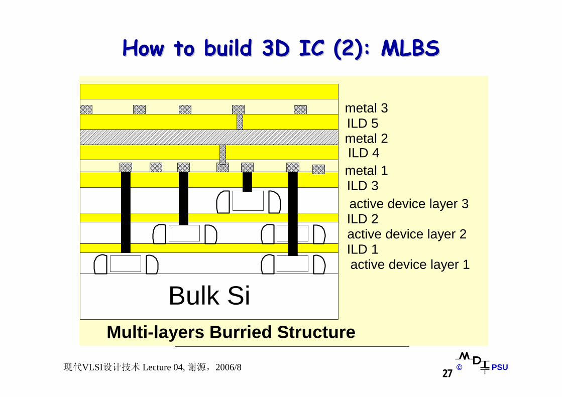
How to build 3D IC (2): MLBSHow to build 3D IC (2): MLBS
Bulk Si
Multi-layers Burried Structure
Bulk Si
ILD 1
ILD 2
ILD 3
active device layer 1
active device layer 2
active device layer 3
metal 1ILD 4metal 2ILD 5metal 3
Multi-layers Burried Structure
© PSU28现代VLSI设计技术 Lecture 04, 谢源,2006/8
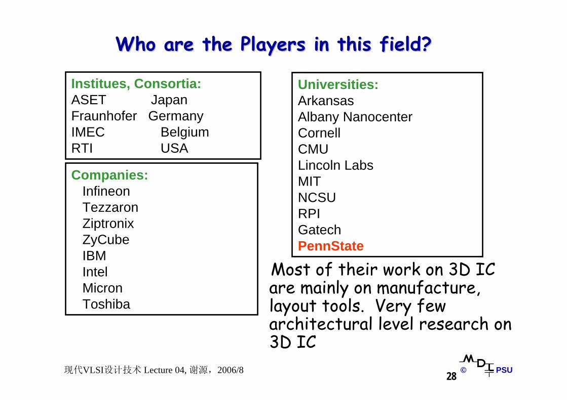
Who are the Players in this field?Who are the Players in this field?
Institues, Consortia:ASET JapanFraunhofer GermanyIMEC BelgiumRTI USA
Companies:InfineonTezzaronZiptronixZyCubeIBMIntelMicronToshiba
Universities:ArkansasAlbany NanocenterCornellCMULincoln LabsMITNCSURPIGatechPennState
Most of their work on 3D IC are mainly on manufacture, layout tools. Very few architectural level research on 3D IC
© PSU29现代VLSI设计技术 Lecture 04, 谢源,2006/8
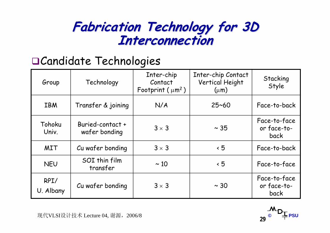
Fabrication Technology for 3D Fabrication Technology for 3D InterconnectionInterconnection
Candidate Technologies
Face-to-back25~60N/ATransfer & joiningIBM
Face-to-face< 5~ 10SOI thin film transferNEU
Face-to-face or face-to-
back~ 303 × 3Cu wafer bonding
RPI/U. Albany
Face-to-back< 53 × 3Cu wafer bondingMIT
Face-to-face or face-to-
back~ 353 × 3Buried-contact +
wafer bondingTohoku Univ.
Stacking Style
Inter-chip Contact Vertical Height
(µm)
Inter-chip Contact
Footprint ( µm2 )TechnologyGroup
© PSU30现代VLSI设计技术 Lecture 04, 谢源,2006/8
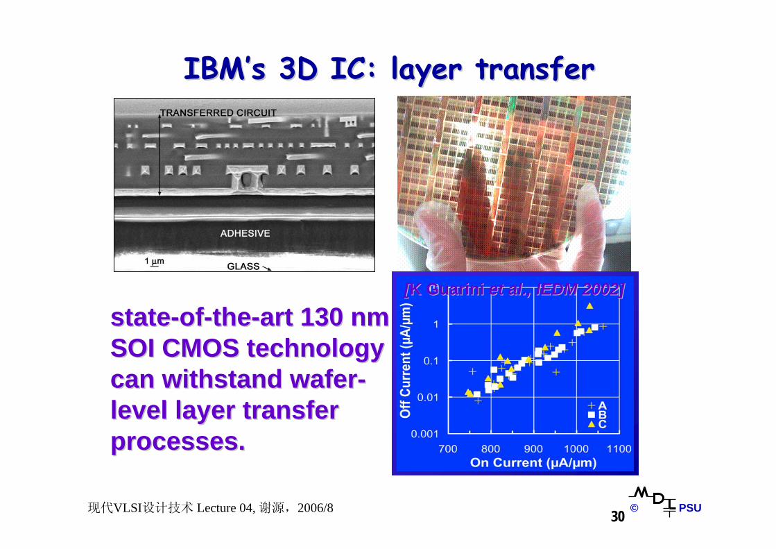
IBMIBM’’s 3D IC: layer transfer s 3D IC: layer transfer
statestate--ofof--thethe--art 130 nm art 130 nm SOI CMOS technology SOI CMOS technology can withstand wafercan withstand wafer--level layer transfer level layer transfer processes.processes.
[[K K GuariniGuarini et al., IEDM 2002]et al., IEDM 2002]
© PSU31现代VLSI设计技术 Lecture 04, 谢源,2006/8
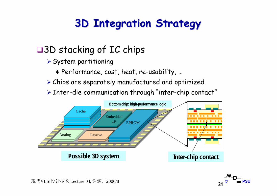
3D Integration Strategy3D Integration Strategy
3D stacking of IC chipsSystem partitioning
Performance, cost, heat, re-usability, …Chips are separately manufactured and optimizedInter-die communication through “inter-chip contact”
Possible 3D system
Cache
PassiveAnalog
Embedded µP EPROM
Inter-chip contact
Bottom chip: high-performance logic
© PSU32现代VLSI设计技术 Lecture 04, 谢源,2006/8
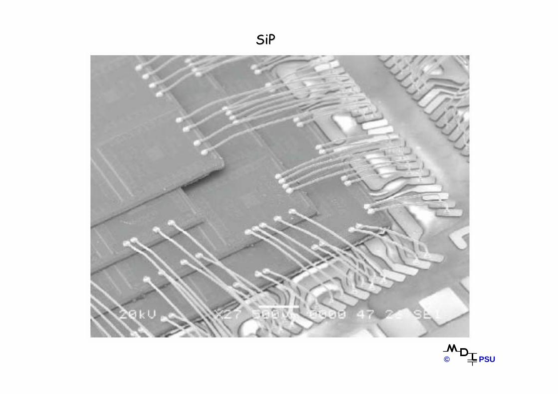
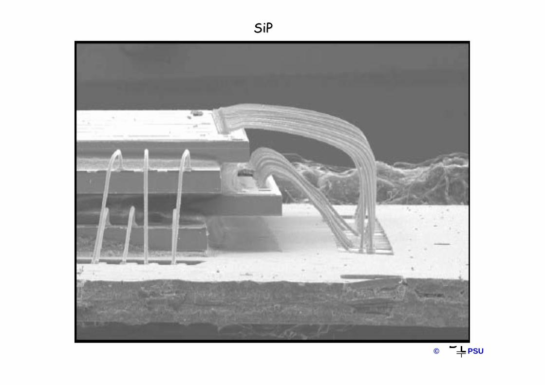
SiPSiP vs. True 3D ICvs. True 3D IC
© PSU
SiPSiP
© PSU
SiPSiP
© PSU38现代VLSI设计技术 Lecture 04, 谢源,2006/8
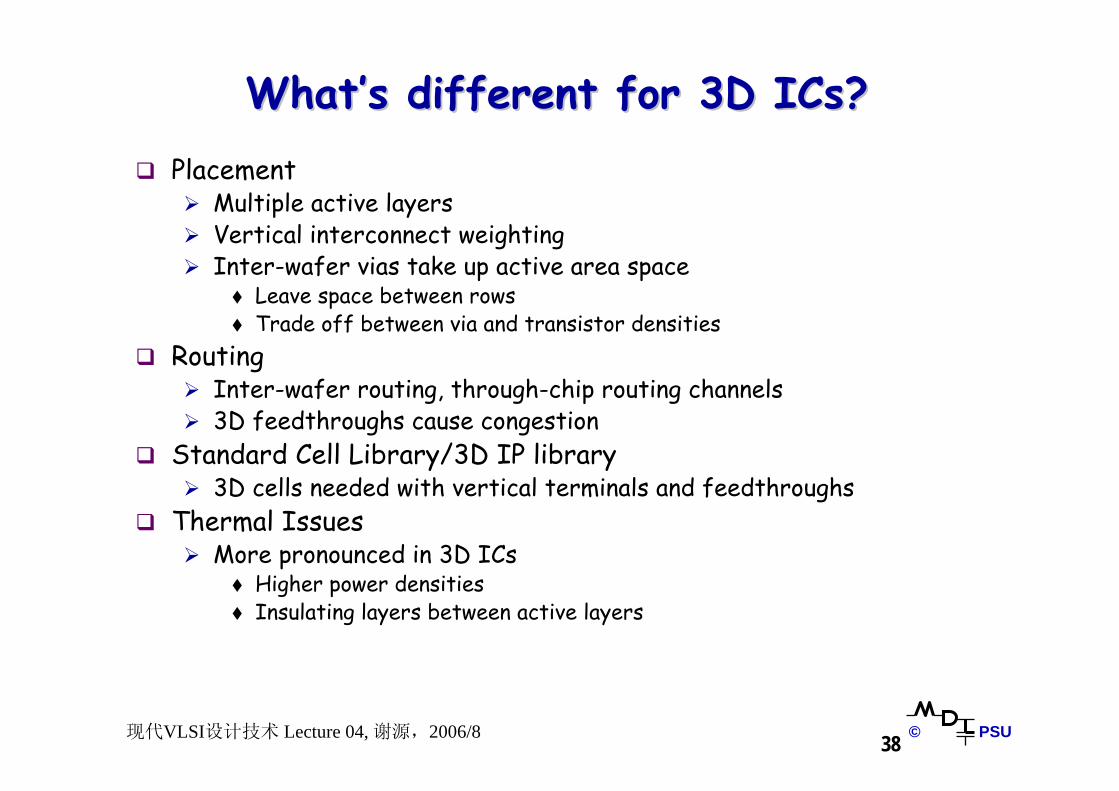
WhatWhat’’s different for 3D ICs?s different for 3D ICs?Placement
Multiple active layersVertical interconnect weightingInter-wafer vias take up active area space
Leave space between rowsTrade off between via and transistor densities
RoutingInter-wafer routing, through-chip routing channels3D feedthroughs cause congestion
Standard Cell Library/3D IP library3D cells needed with vertical terminals and feedthroughs
Thermal IssuesMore pronounced in 3D ICs
Higher power densitiesInsulating layers between active layers
© PSU39现代VLSI设计技术 Lecture 04, 谢源,2006/8
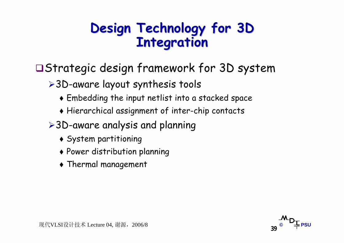
Design Technology for 3D Design Technology for 3D IntegrationIntegration
Strategic design framework for 3D system3D-aware layout synthesis tools
Embedding the input netlist into a stacked spaceHierarchical assignment of inter-chip contacts
3D-aware analysis and planningSystem partitioningPower distribution planningThermal management
© PSU40现代VLSI设计技术 Lecture 04, 谢源,2006/8
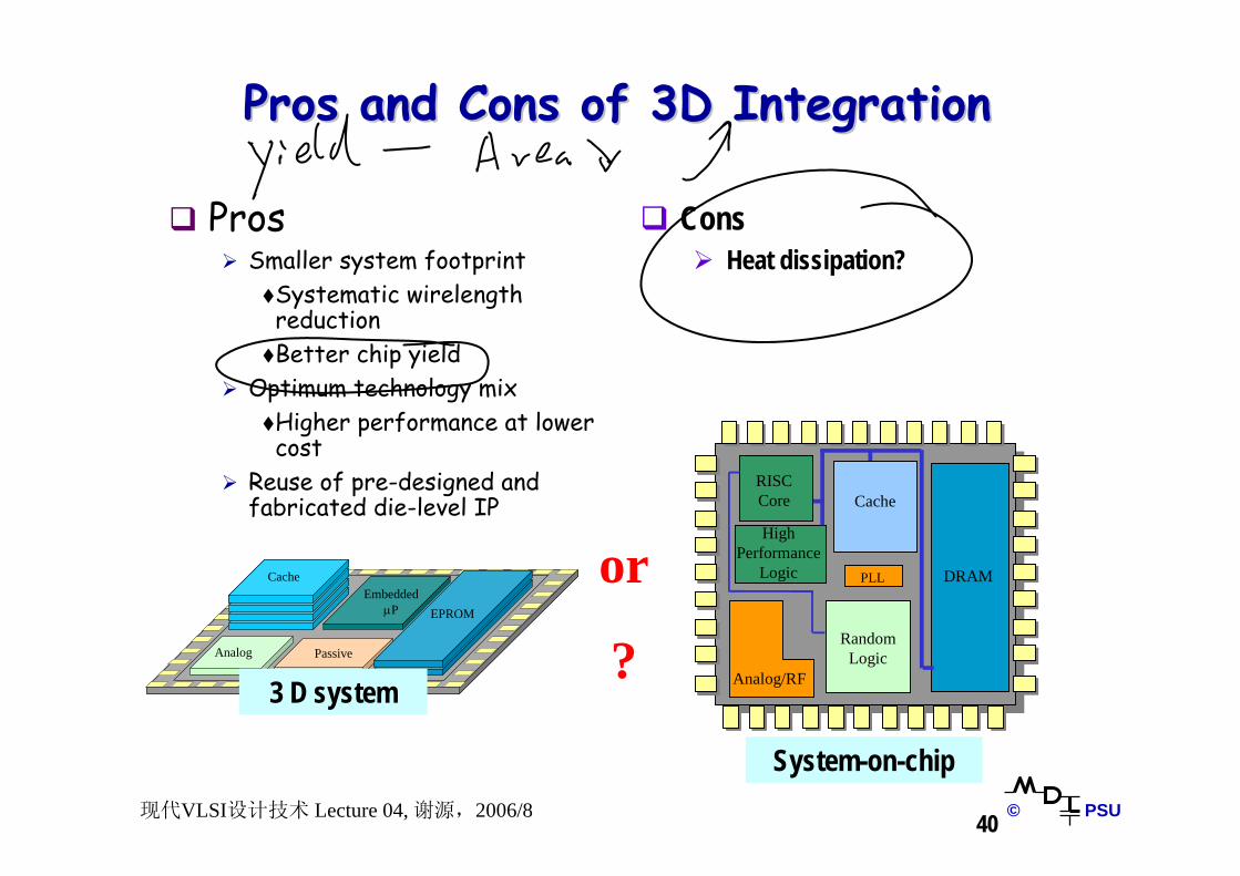
Pros and Cons of 3D IntegrationPros and Cons of 3D Integration
ProsSmaller system footprint
Systematic wirelength reductionBetter chip yield
Optimum technology mixHigher performance at lower cost
Reuse of pre-designed and fabricated die-level IP
System-on-chip
ConsHeat dissipation?
Cache
PassiveAnalog
Embedded µP EPROM
Cache
PassiveAnalog
Embedded µP EPROM
DRAM
RISC Core
PLL
High Performance
Logic
Random Logic
Cache
Analog/RF
DRAM
RISC Core
PLL
High Performance
Logic
Random Logic
CacheCache
Analog/RF3 D system
or
?
© PSU41现代VLSI设计技术 Lecture 04, 谢源,2006/8
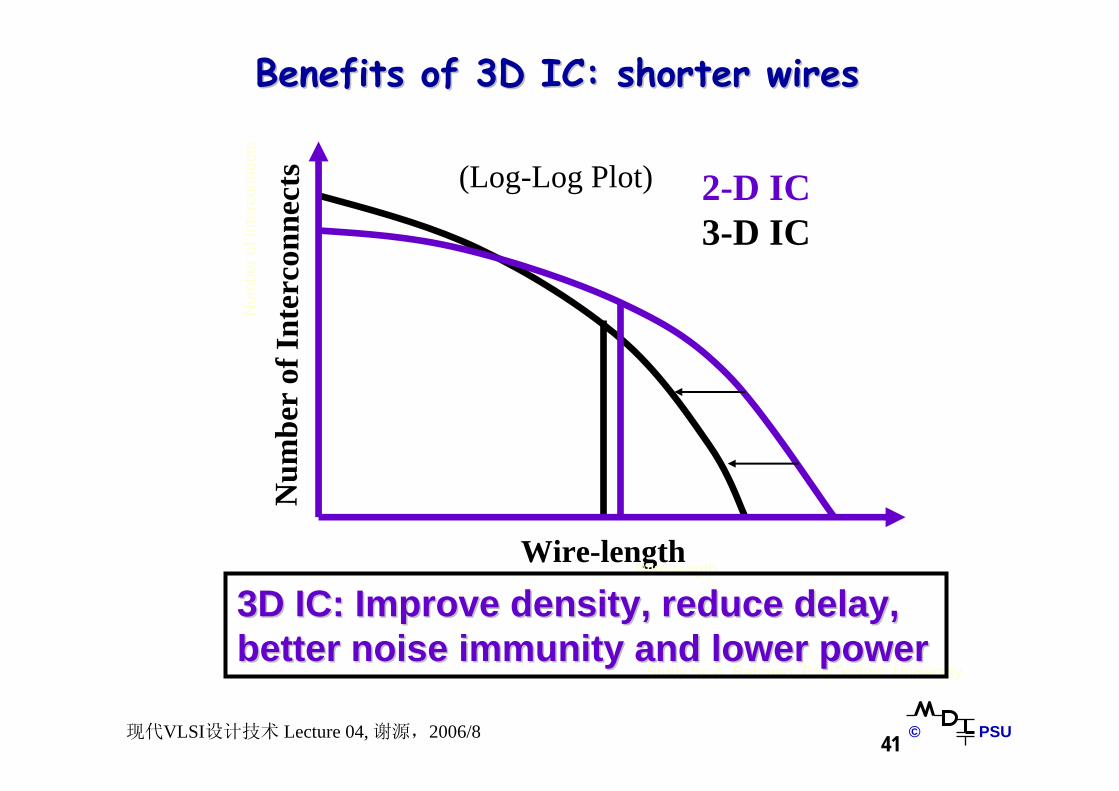
Wire-length
Num
ber
of In
ter c
onne
cts (Log-Log Plot) 2-D IC
3-D IC
Wire-length
Num
ber o
f Int
erco
nnec
ts
Study by A. Rahman, PolyTechnic University
Benefits of 3D IC: shorter wiresBenefits of 3D IC: shorter wires
3D IC: Improve density, reduce delay, 3D IC: Improve density, reduce delay, better noise immunity and lower powerbetter noise immunity and lower power
© PSU42现代VLSI设计技术 Lecture 04, 谢源,2006/8
Performance Improvement of 3D ICsPerformance Improvement of 3D ICs
Reduced WirelengthTotal Wirelength
28% for 2 layers, 51% for 5 layers [Das et al., ISVLSI, 2003]Longest Wirelength
31% for 2 layers, 56% for 5 layers [Das et al., ISVLSI, 2003]More Layers Produce More ImprovementLarger Circuit Sizes Produce More Improvement
[Obenaus and Szymanski, TODAES, July 2003]Higher Transistor Packing DensitiesSmaller Chip AreaLower Power per TransistorDecreased Interconnect Delay
© PSU43现代VLSI设计技术 Lecture 04, 谢源,2006/8
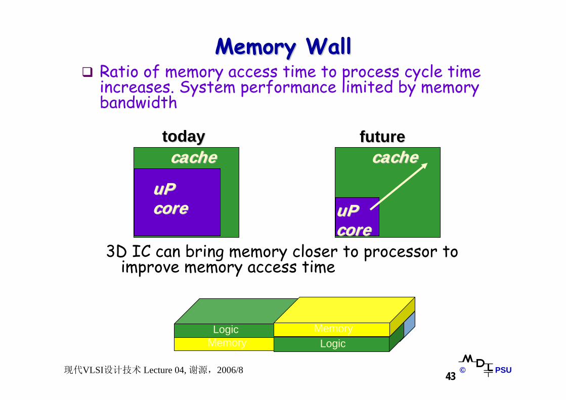
Memory WallMemory WallRatio of memory access time to process cycle time increases. System performance limited by memory bandwidth
3D IC can bring memory closer to processor to improve memory access time
MemoryLogic
LogicMemory
uPuPuPuPcorecore
cachecache cachecache
uPuPcorecore
todaytoday futurefuture
© PSU45现代VLSI设计技术 Lecture 04, 谢源,2006/8
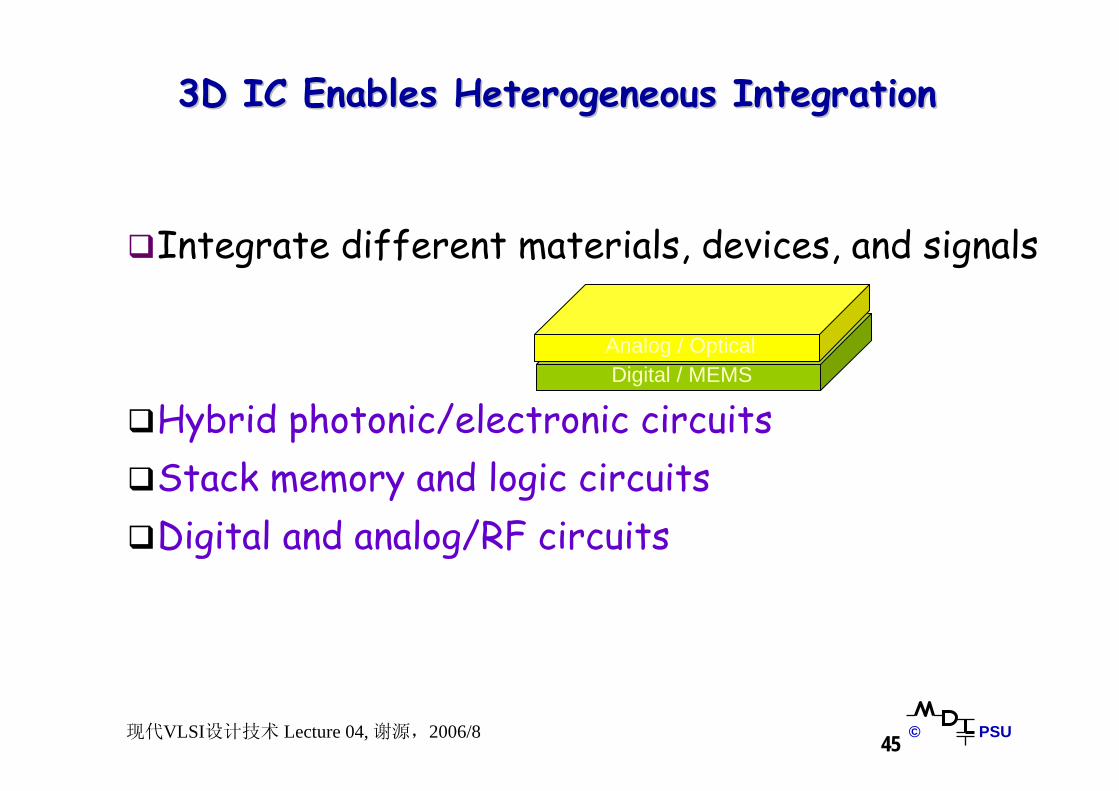
3D IC Enables Heterogeneous Integration3D IC Enables Heterogeneous Integration
Integrate different materials, devices, and signals
Hybrid photonic/electronic circuitsStack memory and logic circuitsDigital and analog/RF circuits
Digital / MEMSAnalog / Optical
© PSU46现代VLSI设计技术 Lecture 04, 谢源,2006/8
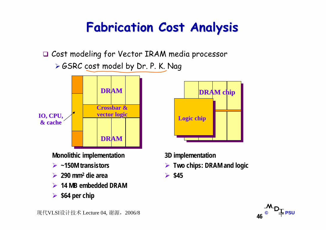
Fabrication Cost AnalysisFabrication Cost Analysis
Cost modeling for Vector IRAM media processorGSRC cost model by Dr. P. K. Nag
DRAMDRAM
DRAMDRAM
Crossbar & Crossbar & vector logicvector logicIO, CPU,IO, CPU,
& cache& cache
Monolithic implementation~150M transistors290 mm2 die area14 MB embedded DRAM$64 per chip
3D implementationTwo chips: DRAM and logic$45
DRAM chipDRAM chip
Logic chipLogic chip
© PSU
Panel Discussion:Panel Discussion:Temperature: A showstopper for 3D Temperature: A showstopper for 3D
Architecture?Architecture?
Yuan XieThe Pennsylvania State University
Department of Computer Science & [email protected]
The 3rd Temperature-Aware Computer Systems Workshop (TACS), 2006
© PSU48现代VLSI设计技术 Lecture 04, 谢源,2006/8
Key EDA Challenges to Enable 3D Architecture Under the TemperatuKey EDA Challenges to Enable 3D Architecture Under the Temperature re ConstraintsConstraints
Tools for Early Analysis
To estimate temperature (e.g. HS3D, HotSpot)
To study the tradeoff: performance vs. power vs. temperature (e.g. 3DCacti @ ICCD 2005)
-- How many layers? -- Power reduction benefits from 3D may help
mitigate thermal issues(e.g. Intel @ ICCD 2005)
© PSU49现代VLSI设计技术 Lecture 04, 谢源,2006/8
Key EDA Challenges to Enable 3D Architecture Under the TemperatuKey EDA Challenges to Enable 3D Architecture Under the Temperature re ConstraintsConstraints
Tools for Physical Design
3D Physical Design tools must be thermal-aware Vertical optimizationHorizontal optimization
(e.g. 3D FP @ ISQED 2006)
Thermal Via planning (similar to the elevator in high-rise) (e.g. GIT/UMN/UCLA research)


![Section 8 1-CCD.ppt [Λειτουργία συμβατότητας]tsiatouhas/CCD/Section_8_1-2p.pdf · 1 CMOSCMOS INTEGRATED INTEGRATED CIRCUIT DESIGN TECHNIQUES University of Ioannina](https://static.fdocument.org/doc/165x107/5adb58097f8b9a86378e87f8/section-8-1-ccdppt-tsiatouhasccdsection81-2ppdf1.jpg)