Lecture 27: Non-Linear Power...
32
EECS 142 Lecture 27: Non-Linear Power Amplifiers Prof. Ali M. Niknejad University of California, Berkeley Copyright c 2005 by Ali M. Niknejad A. M. Niknejad University of California, Berkeley EECS 142 Lecture 27 p. 1/32
-
Upload
nguyennhan -
Category
Documents
-
view
222 -
download
0
Transcript of Lecture 27: Non-Linear Power...
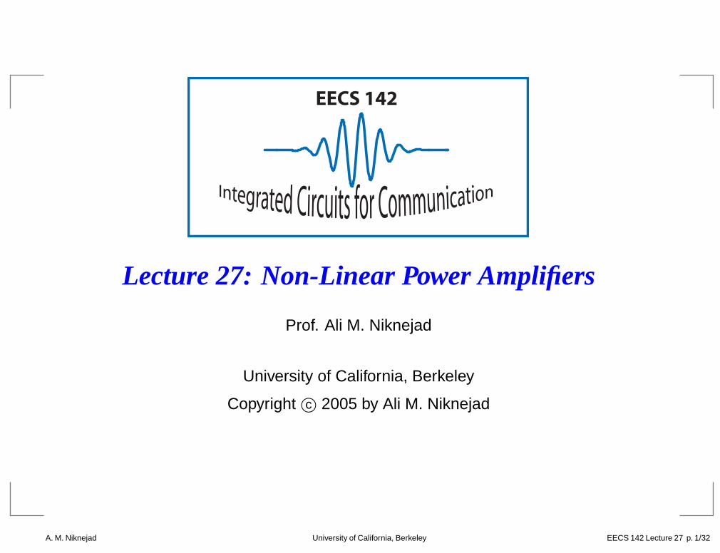
EECS 142
Lecture 27: Non-Linear Power Amplifiers
Prof. Ali M. Niknejad
University of California, Berkeley
Copyright c© 2005 by Ali M. Niknejad
A. M. Niknejad University of California, Berkeley EECS 142 Lecture 27 p. 1/32 – p. 1/32
Efficiency of Class A
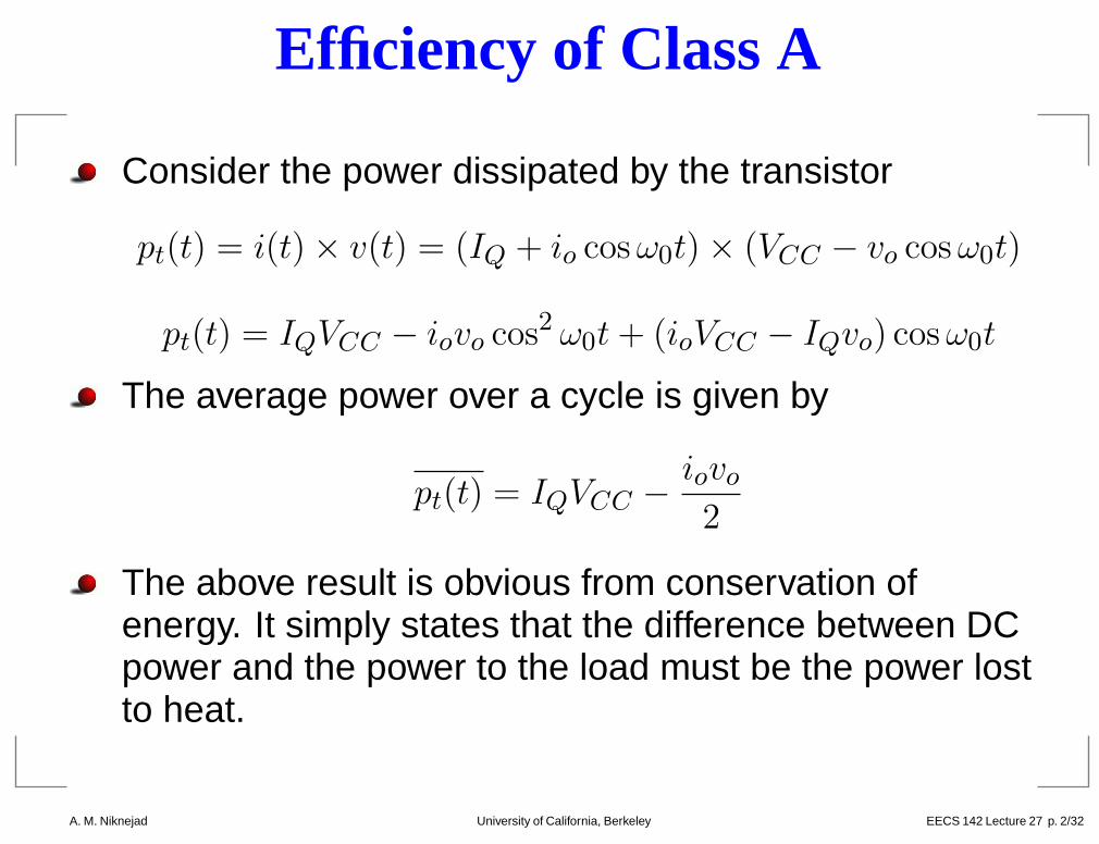
Consider the power dissipated by the transistor
pt(t) = i(t) × v(t) = (IQ + io cos ω0t) × (VCC − vo cos ω0t)
pt(t) = IQVCC − iovo cos2 ω0t + (ioVCC − IQvo) cos ω0t
The average power over a cycle is given by
pt(t) = IQVCC −iovo
2
The above result is obvious from conservation ofenergy. It simply states that the difference between DCpower and the power to the load must be the power lostto heat.
A. M. Niknejad University of California, Berkeley EECS 142 Lecture 27 p. 2/32 – p. 2/32
Efficiency Cont
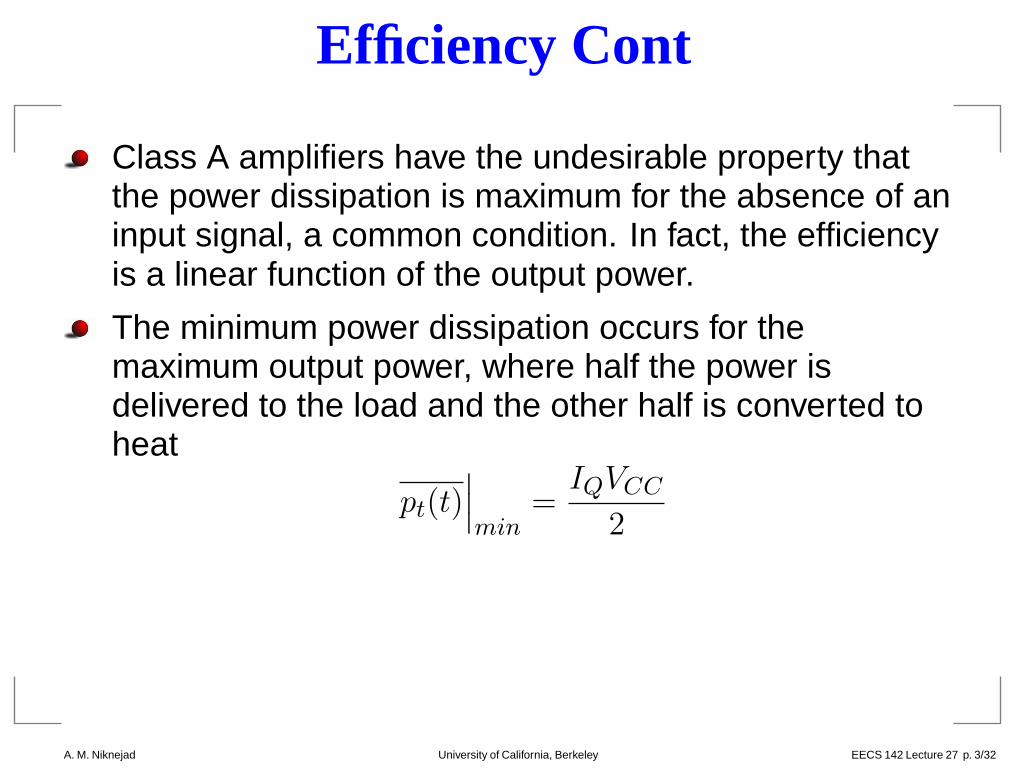
Class A amplifiers have the undesirable property thatthe power dissipation is maximum for the absence of aninput signal, a common condition. In fact, the efficiencyis a linear function of the output power.
The minimum power dissipation occurs for themaximum output power, where half the power isdelivered to the load and the other half is converted toheat
pt(t)∣
∣
∣
min=
IQVCC
2
A. M. Niknejad University of California, Berkeley EECS 142 Lecture 27 p. 3/32 – p. 3/32
Average Efficiency
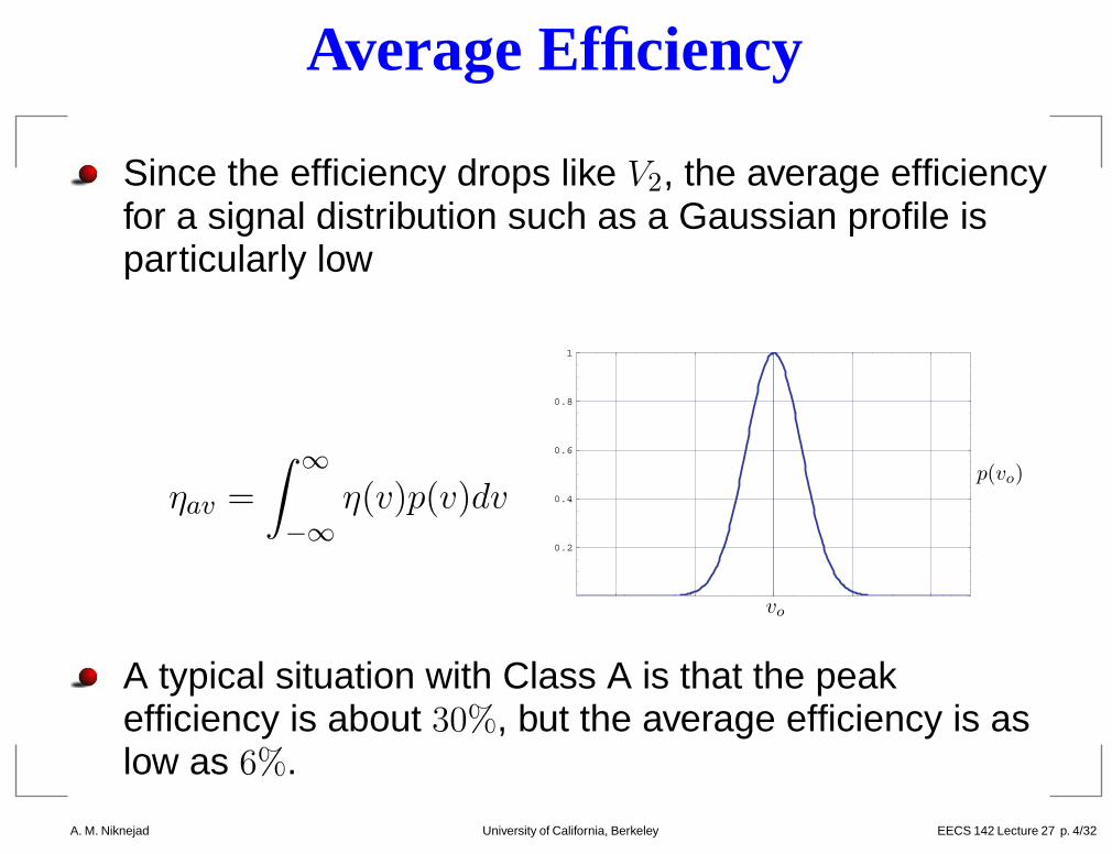
Since the efficiency drops like V2, the average efficiencyfor a signal distribution such as a Gaussian profile isparticularly low
ηav =
∫
∞
−∞
η(v)p(v)dv0.2
0.4
0.6
0.8
1
p(vo)
vo
A typical situation with Class A is that the peakefficiency is about 30%, but the average efficiency is aslow as 6%.
A. M. Niknejad University of California, Berkeley EECS 142 Lecture 27 p. 4/32 – p. 4/32
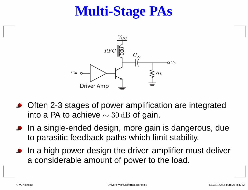
Multi-Stage PAs
vin
vo
VCC
RL
C∞
RFC
Driver Amp
Often 2-3 stages of power amplification are integratedinto a PA to achieve ∼ 30 dB of gain.
In a single-ended design, more gain is dangerous, dueto parasitic feedback paths which limit stability.
In a high power design the driver amplifier must delivera considerable amount of power to the load.
A. M. Niknejad University of California, Berkeley EECS 142 Lecture 27 p. 5/32 – p. 5/32
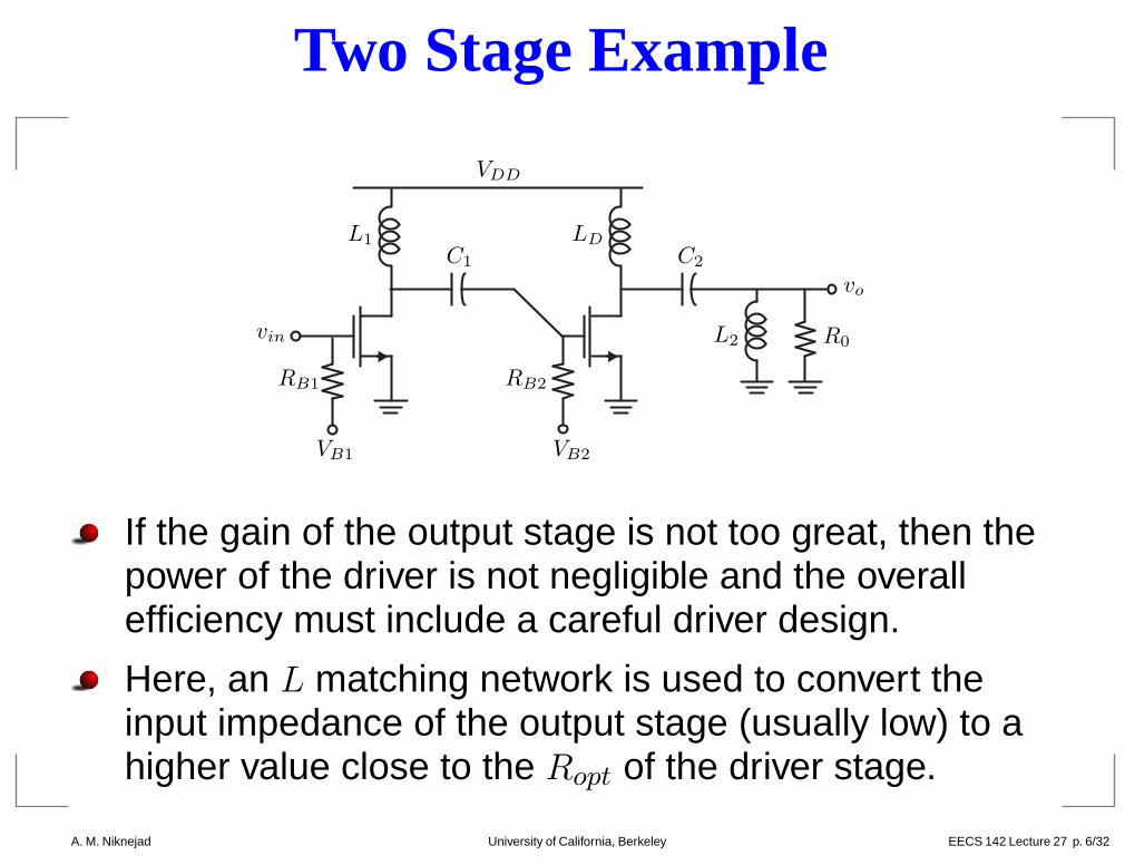
Two Stage Example
vin
vo
R0
VDD
L1
C1
L2
C2
RB1 RB2
LD
VB1 VB2
If the gain of the output stage is not too great, then thepower of the driver is not negligible and the overallefficiency must include a careful driver design.
Here, an L matching network is used to convert theinput impedance of the output stage (usually low) to ahigher value close to the Ropt of the driver stage.
A. M. Niknejad University of California, Berkeley EECS 142 Lecture 27 p. 6/32 – p. 6/32
Class B PA
+vin
VCCvbias
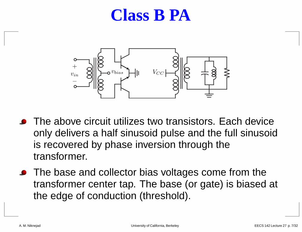
The above circuit utilizes two transistors. Each deviceonly delivers a half sinusoid pulse and the full sinusoidis recovered by phase inversion through thetransformer.
The base and collector bias voltages come from thetransformer center tap. The base (or gate) is biased atthe edge of conduction (threshold).
A. M. Niknejad University of California, Berkeley EECS 142 Lecture 27 p. 7/32 – p. 7/32
Class B Operation
p(t)
ic(t) vc(t)
VCC
0V
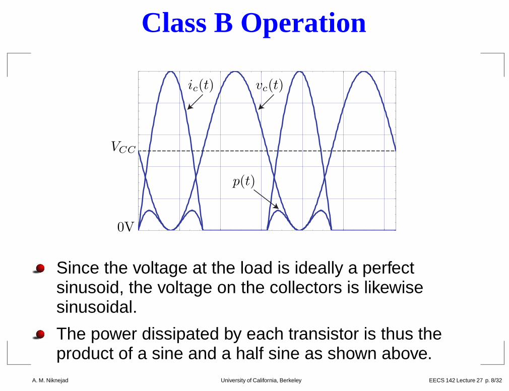
Since the voltage at the load is ideally a perfectsinusoid, the voltage on the collectors is likewisesinusoidal.
The power dissipated by each transistor is thus theproduct of a sine and a half sine as shown above.
A. M. Niknejad University of California, Berkeley EECS 142 Lecture 27 p. 8/32 – p. 8/32
Efficiency of Class B
The average current drawn by each transistor is givenby
IQ =1
T
∫ T
0
ic(t)dt =Ip
T
∫ T/2
0
sin ωtdt =Ip
2π
∫ π
0
sin θdθ =Ip
π
Where Ip is the peak voltage drawn from the supply.
The peak current drawn from the supply is just the loadcurrent swing reflected to the collector, Ip = io × n.
η =1
2
(
Ip
2IQ
) (
vo
VCC
)
Note that the total DC current draw is twice IQ sinceboth devices draw current from the supply.
A. M. Niknejad University of California, Berkeley EECS 142 Lecture 27 p. 9/32 – p. 9/32
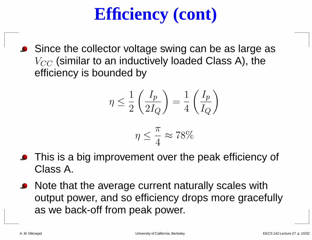
Efficiency (cont)
Since the collector voltage swing can be as large asVCC (similar to an inductively loaded Class A), theefficiency is bounded by
η ≤1
2
(
Ip
2IQ
)
=1
4
(
Ip
IQ
)
η ≤π
4≈ 78%
This is a big improvement over the peak efficiency ofClass A.
Note that the average current naturally scales withoutput power, and so efficiency drops more gracefullyas we back-off from peak power.
A. M. Niknejad University of California, Berkeley EECS 142 Lecture 27 p. 10/32 – p
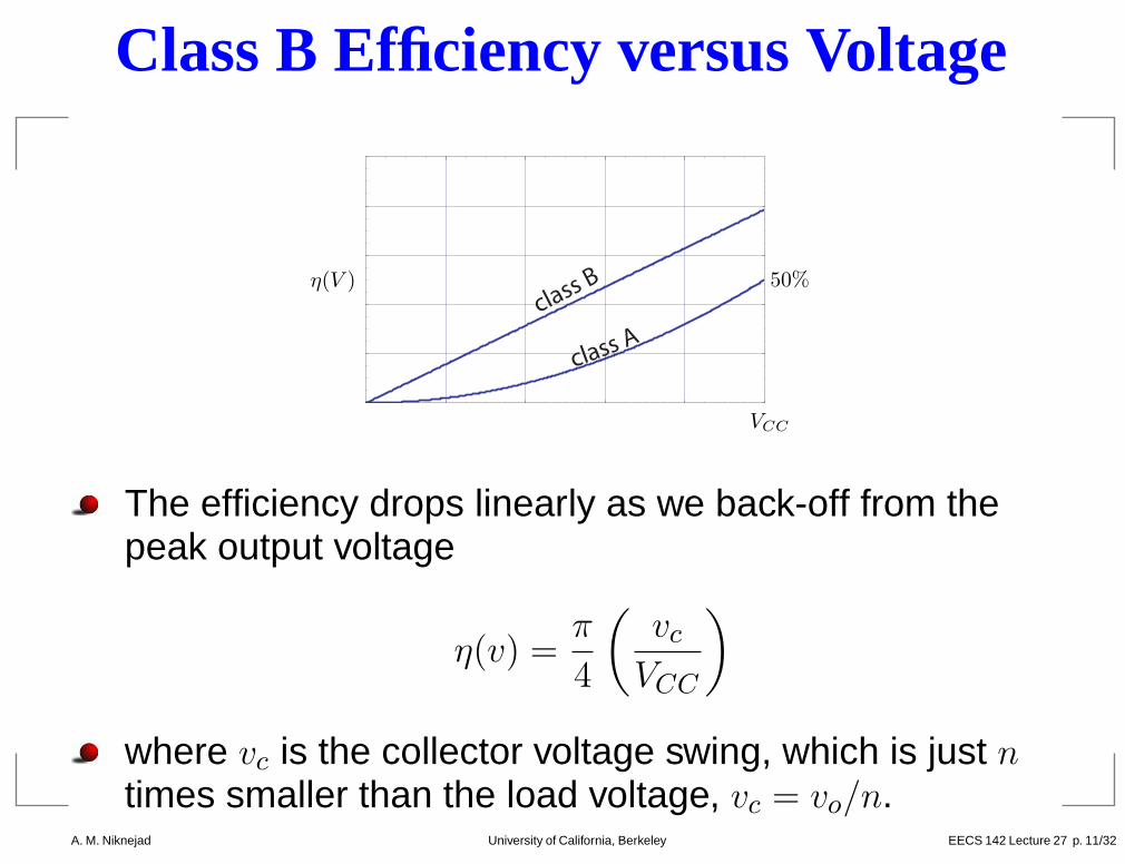
Class B Efficiency versus Voltage
η(V )
VCC
50%class B
class A
The efficiency drops linearly as we back-off from thepeak output voltage
η(v) =π
4
(
vc
VCC
)
where vc is the collector voltage swing, which is just ntimes smaller than the load voltage, vc = vo/n.
A. M. Niknejad University of California, Berkeley EECS 142 Lecture 27 p. 11/32 – p
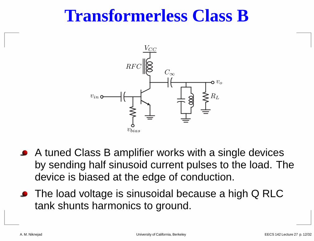
Transformerless Class B
vin
vo
VCC
RL
C∞
RFC
vbias
A tuned Class B amplifier works with a single devicesby sending half sinusoid current pulses to the load. Thedevice is biased at the edge of conduction.
The load voltage is sinusoidal because a high Q RLCtank shunts harmonics to ground.
A. M. Niknejad University of California, Berkeley EECS 142 Lecture 27 p. 12/32 – p
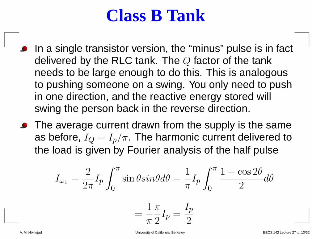
Class B Tank
In a single transistor version, the “minus” pulse is in factdelivered by the RLC tank. The Q factor of the tankneeds to be large enough to do this. This is analogousto pushing someone on a swing. You only need to pushin one direction, and the reactive energy stored willswing the person back in the reverse direction.
The average current drawn from the supply is the sameas before, IQ = Ip/π. The harmonic current delivered tothe load is given by Fourier analysis of the half pulse
Iω1=
2
2πIp
∫ π
0
sin θsinθdθ =1
πIp
∫ π
0
1 − cos 2θ
2dθ
=1
π
π
2Ip =
Ip
2A. M. Niknejad University of California, Berkeley EECS 142 Lecture 27 p. 13/32 – p
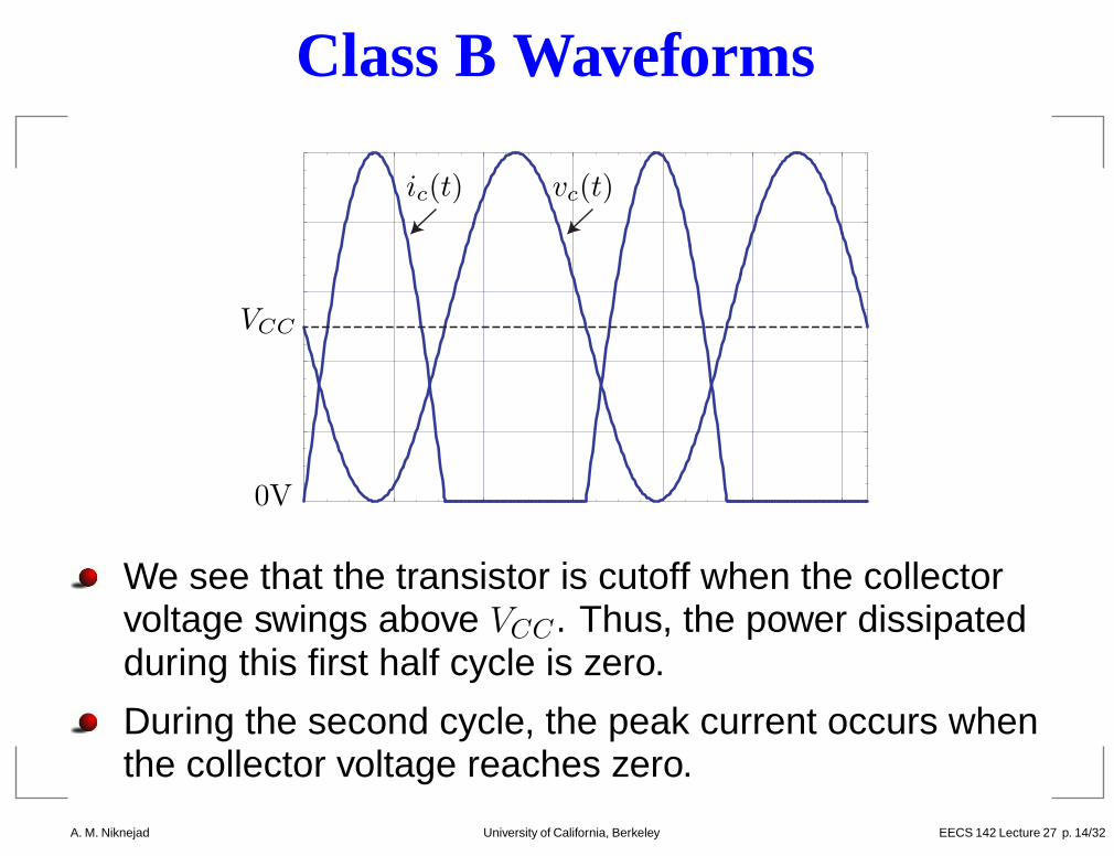
Class B Waveforms
ic(t) vc(t)
VCC
0V
We see that the transistor is cutoff when the collectorvoltage swings above VCC . Thus, the power dissipatedduring this first half cycle is zero.
During the second cycle, the peak current occurs whenthe collector voltage reaches zero.
A. M. Niknejad University of California, Berkeley EECS 142 Lecture 27 p. 14/32 – p
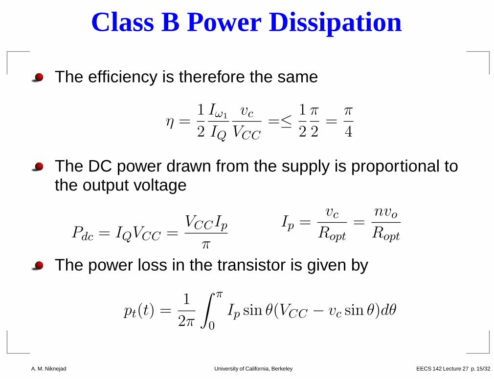
Class B Power Dissipation
The efficiency is therefore the same
η =1
2
Iω1
IQ
vc
VCC=≤
1
2
π
2=
π
4
The DC power drawn from the supply is proportional tothe output voltage
Pdc = IQVCC =VCCIp
π
Ip =vc
Ropt=
nvo
Ropt
The power loss in the transistor is given by
pt(t) =1
2π
∫ π
0
Ip sin θ(VCC − vc sin θ)dθ
A. M. Niknejad University of California, Berkeley EECS 142 Lecture 27 p. 15/32 – p
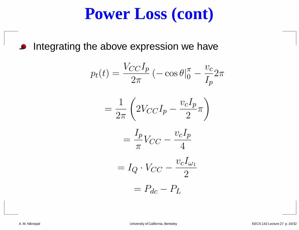
Power Loss (cont)
Integrating the above expression we have
pt(t) =VCCIp
2π(− cos θ|π
0−
vc
Ip2π
=1
2π
(
2VCCIp −vcIp
2π
)
=Ip
πVCC −
vcIp
4
= IQ · VCC −vcIω1
2
= Pdc − PL
A. M. Niknejad University of California, Berkeley EECS 142 Lecture 27 p. 16/32 – p
Conduction Angle
Often amplifiers are characterized by their conductionangle, or the amount of time the collector current flowsduring a cycle.
Class A amplifiers have 360◦ conduction angle, sincethe DC current is always flowing through the device.
Class B amplifiers, though, have 180◦ conduction angle,since they conduct half sinusoidal pulses.
In practice most Class B amplifiers are implemented asClass AB amplifiers, as a trickle current is allowed toflow through the main device to avoid cutting off thedevice during the amplifier operation.
A. M. Niknejad University of California, Berkeley EECS 142 Lecture 27 p. 17/32 – p
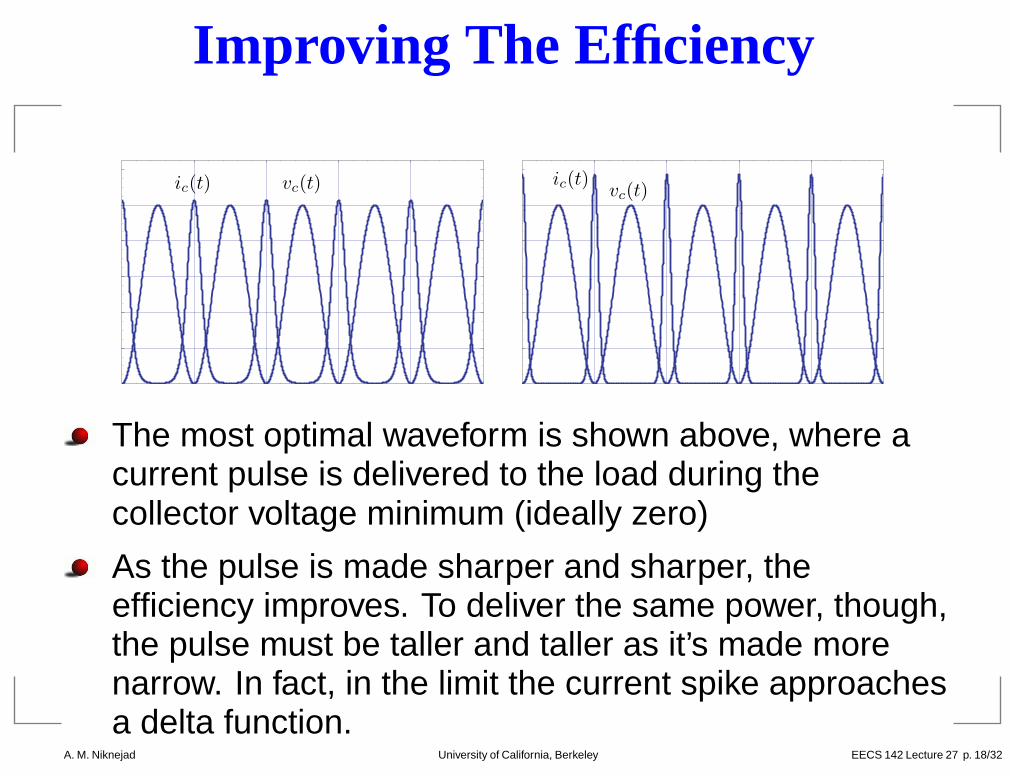
Improving The Efficiency
ic(t) vc(t) ic(t) vc(t)
The most optimal waveform is shown above, where acurrent pulse is delivered to the load during thecollector voltage minimum (ideally zero)
As the pulse is made sharper and sharper, theefficiency improves. To deliver the same power, though,the pulse must be taller and taller as it’s made morenarrow. In fact, in the limit the current spike approachesa delta function.
A. M. Niknejad University of California, Berkeley EECS 142 Lecture 27 p. 18/32 – p
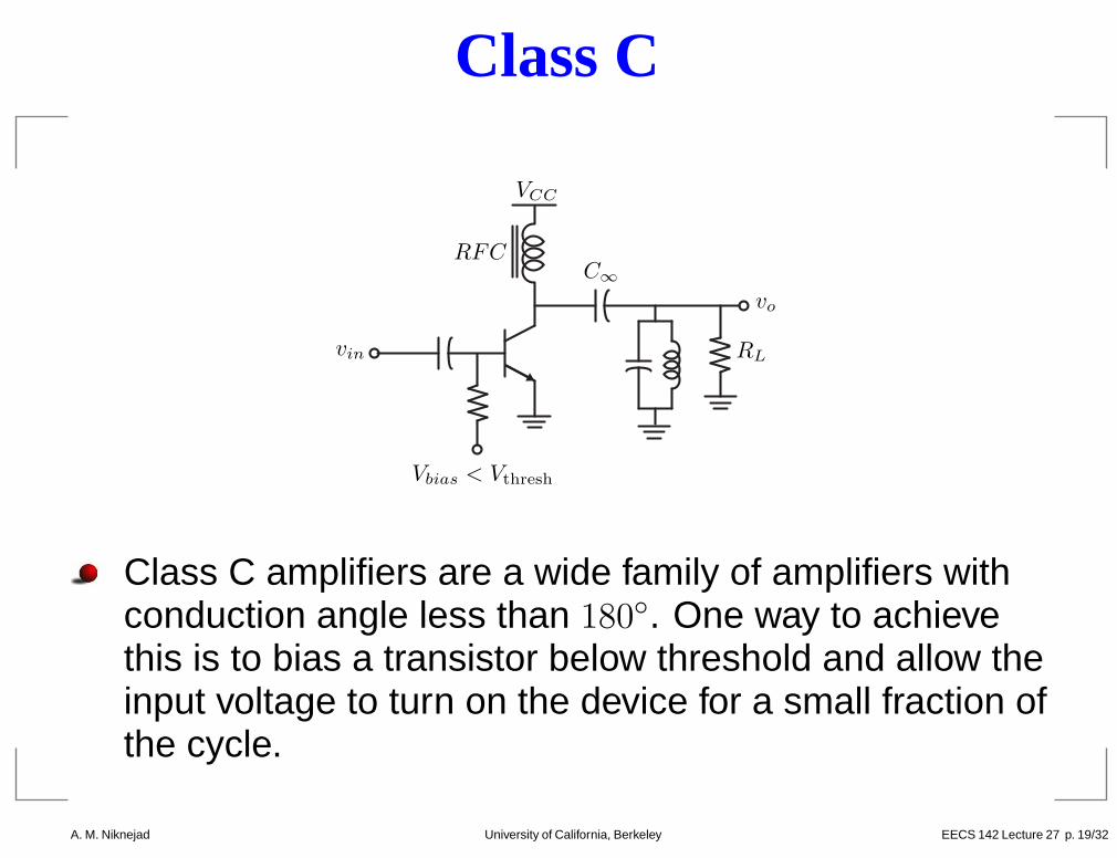
Class C
vin
vo
VCC
RL
C∞
RFC
Vbias < Vthresh
Class C amplifiers are a wide family of amplifiers withconduction angle less than 180◦. One way to achievethis is to bias a transistor below threshold and allow theinput voltage to turn on the device for a small fraction ofthe cycle.
A. M. Niknejad University of California, Berkeley EECS 142 Lecture 27 p. 19/32 – p
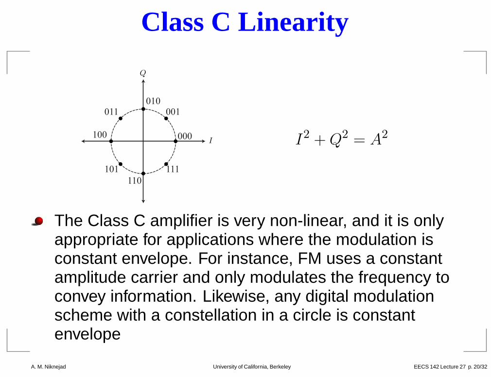
Class C Linearity
I
Q
000
001
010
011
100
101
110
111
I2 + Q2 = A2
The Class C amplifier is very non-linear, and it is onlyappropriate for applications where the modulation isconstant envelope. For instance, FM uses a constantamplitude carrier and only modulates the frequency toconvey information. Likewise, any digital modulationscheme with a constellation in a circle is constantenvelope
A. M. Niknejad University of California, Berkeley EECS 142 Lecture 27 p. 20/32 – p
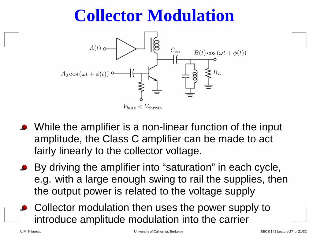
Collector Modulation
RL
C∞
Vbias < Vthresh
B(t) cos (ωt + φ(t))A(t)
A0 cos (ωt + φ(t))
While the amplifier is a non-linear function of the inputamplitude, the Class C amplifier can be made to actfairly linearly to the collector voltage.
By driving the amplifier into “saturation” in each cycle,e.g. with a large enough swing to rail the supplies, thenthe output power is related to the voltage supply
Collector modulation then uses the power supply tointroduce amplitude modulation into the carrier
A. M. Niknejad University of California, Berkeley EECS 142 Lecture 27 p. 21/32 – p
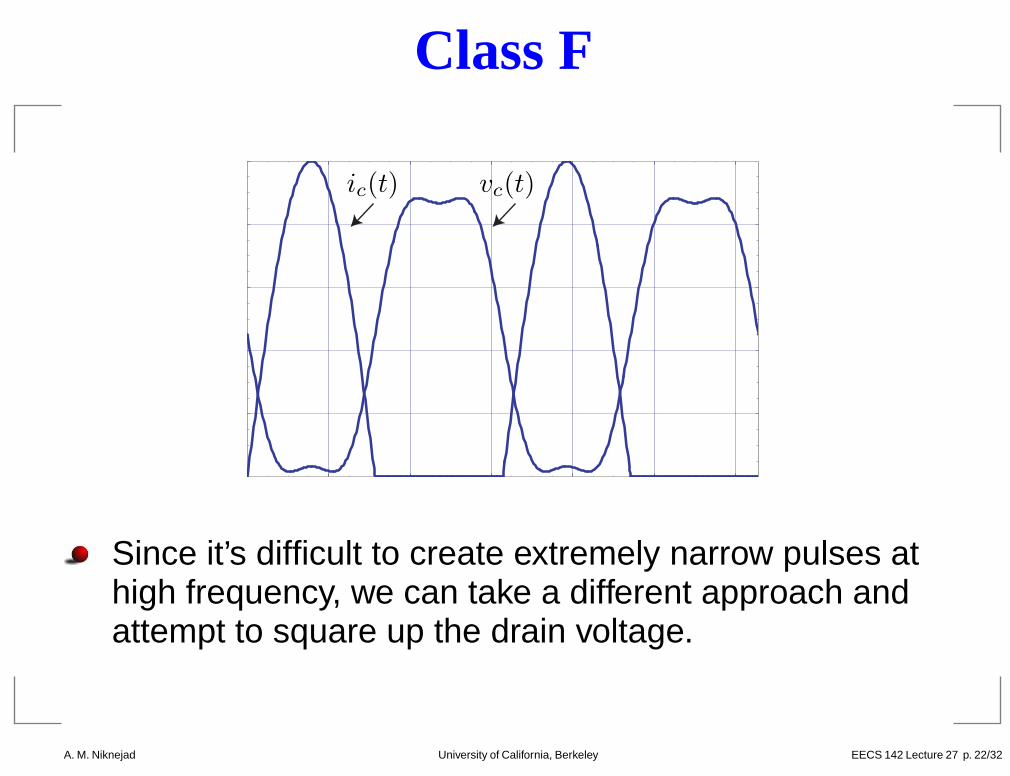
Class F
ic(t) vc(t)
Since it’s difficult to create extremely narrow pulses athigh frequency, we can take a different approach andattempt to square up the drain voltage.
A. M. Niknejad University of California, Berkeley EECS 142 Lecture 27 p. 22/32 – p
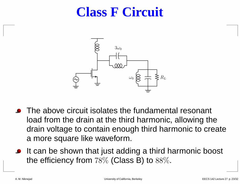
Class F Circuit
3ω0
ω0 RL
The above circuit isolates the fundamental resonantload from the drain at the third harmonic, allowing thedrain voltage to contain enough third harmonic to createa more square like waveform.
It can be shown that just adding a third harmonic boostthe efficiency from 78% (Class B) to 88%.
A. M. Niknejad University of California, Berkeley EECS 142 Lecture 27 p. 23/32 – p
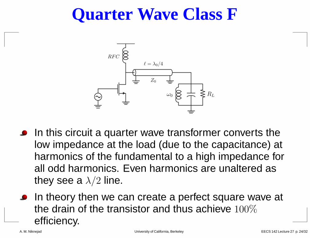
Quarter Wave Class F
ω0 RL
Z0
ℓ = λ0/4
RFC
In this circuit a quarter wave transformer converts thelow impedance at the load (due to the capacitance) atharmonics of the fundamental to a high impedance forall odd harmonics. Even harmonics are unaltered asthey see a λ/2 line.
In theory then we can create a perfect square wave atthe drain of the transistor and thus achieve 100%efficiency.
A. M. Niknejad University of California, Berkeley EECS 142 Lecture 27 p. 24/32 – p
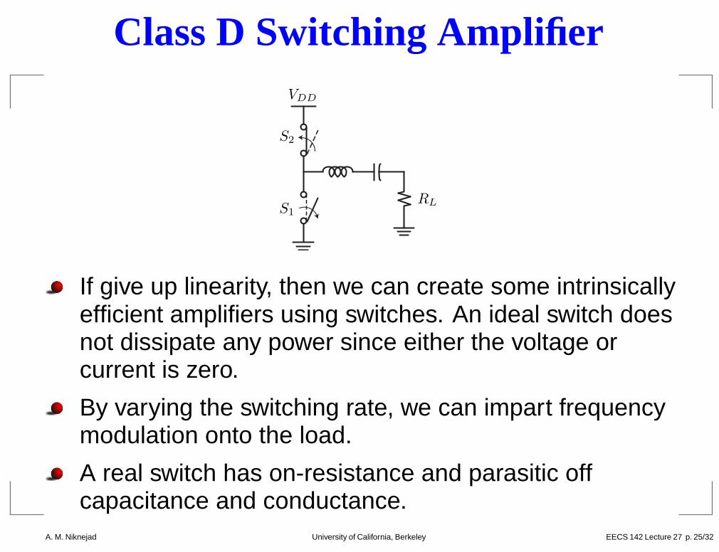
Class D Switching Amplifier
S1
S2
RL
VDD
If give up linearity, then we can create some intrinsicallyefficient amplifiers using switches. An ideal switch doesnot dissipate any power since either the voltage orcurrent is zero.
By varying the switching rate, we can impart frequencymodulation onto the load.
A real switch has on-resistance and parasitic offcapacitance and conductance.
A. M. Niknejad University of California, Berkeley EECS 142 Lecture 27 p. 25/32 – p
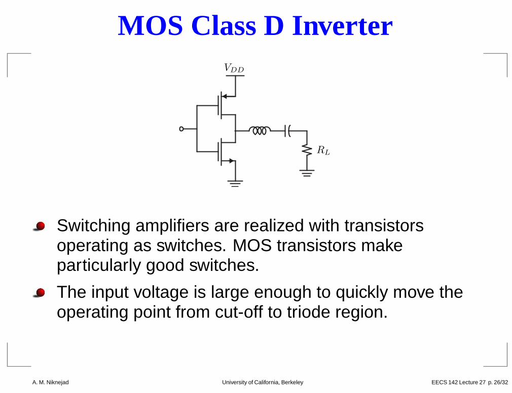
MOS Class D Inverter
RL
VDD
Switching amplifiers are realized with transistorsoperating as switches. MOS transistors makeparticularly good switches.
The input voltage is large enough to quickly move theoperating point from cut-off to triode region.
A. M. Niknejad University of California, Berkeley EECS 142 Lecture 27 p. 26/32 – p
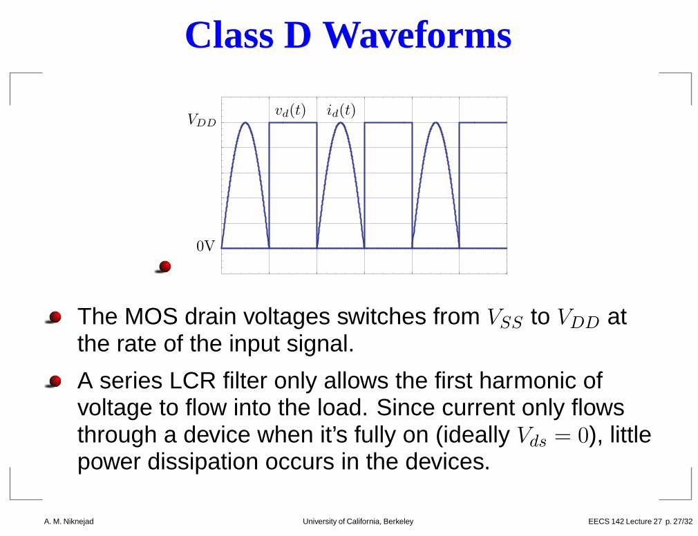
Class D Waveforms
0V
id(t)VDD
vd(t)
The MOS drain voltages switches from VSS to VDD atthe rate of the input signal.
A series LCR filter only allows the first harmonic ofvoltage to flow into the load. Since current only flowsthrough a device when it’s fully on (ideally Vds = 0), littlepower dissipation occurs in the devices.
A. M. Niknejad University of California, Berkeley EECS 142 Lecture 27 p. 27/32 – p
Class D Efficiency
We can see that the efficiency has to be 100% for anideal switch. That’s because there is no where for theDC power to flow except to the load.
The collector voltage can be decomposed into a Fourierseries
vd =VDD
2(1 + s(ωt))
s(θ) = sign(sin(θ)) =4
π
(
sin θ +1
3sin 3θ +
1
5sin 5θ + · · ·
)
The load current is therefore
iL =4
π
VDD
2Rsin θ =
2VDD
πRLsin θ
A. M. Niknejad University of California, Berkeley EECS 142 Lecture 27 p. 28/32 – p
Class D Efficiency (cont)
The load power is thus
PL =i2LRL
2=
2
π2
V 2
DD
RL≈ 0.2
V 2
DD
RL
The drain current are half-sinusoid pulses. The averagecurrent drawn from the supply is the average PMOScurrent
IQ =Ip
π=
2
π2
VDD
RL
PDC = IQ · VDD =2V 2
DD
π2RL= PL
As we expected, the ideal efficiency is η = 100%
A. M. Niknejad University of California, Berkeley EECS 142 Lecture 27 p. 29/32 – p
Class D Losses
As previously noted, a real Class D amplifier efficiencyis lowered due to the switch on-resistance
We can make our switches bigger to minimize theresistance, but this in turn increases the parasiticcapacitance
There are two forms of loss associated with theparasitic capacitance, the capacitor charging lossesCV 2f and the parasitic substrate losses.
The power required to drive the switches also increasesproportional to Cgs since we have to burn CV 2f powerto drive the inverter or. A resonant drive can lower thedrive power by the Q of the resonator.
In practice a careful balance dictates the maximumswitch size
A. M. Niknejad University of California, Berkeley EECS 142 Lecture 27 p. 30/32 – p
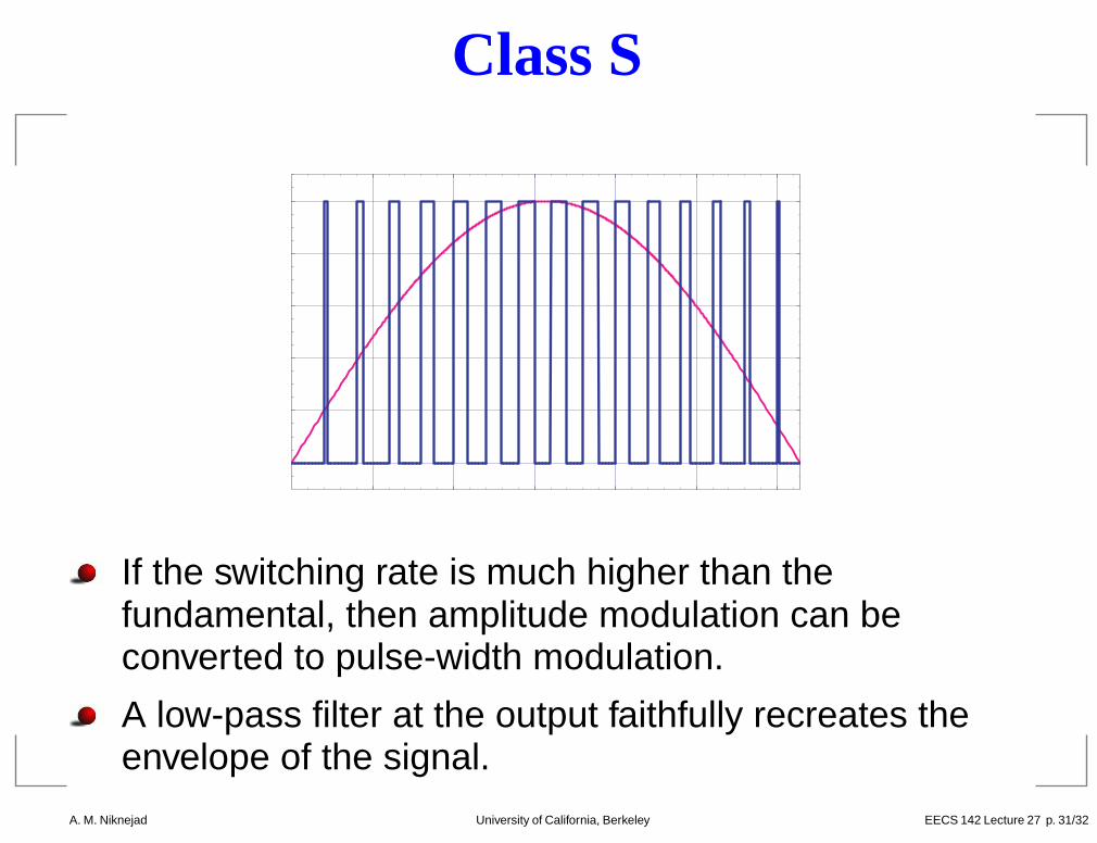
Class S
If the switching rate is much higher than thefundamental, then amplitude modulation can beconverted to pulse-width modulation.
A low-pass filter at the output faithfully recreates theenvelope of the signal.
A. M. Niknejad University of California, Berkeley EECS 142 Lecture 27 p. 31/32 – p
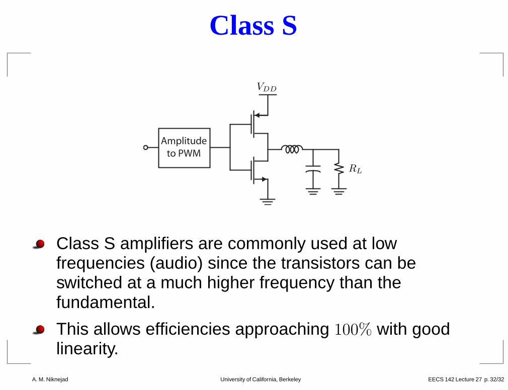
Class S
RL
VDD
Amplitude
to PWM
Class S amplifiers are commonly used at lowfrequencies (audio) since the transistors can beswitched at a much higher frequency than thefundamental.
This allows efficiencies approaching 100% with goodlinearity.
A. M. Niknejad University of California, Berkeley EECS 142 Lecture 27 p. 32/32 – p