
Lecture 2 - Variation-Tolerant Design of Analog CMOS ...
64
Variation-Tolerant Design of Analog CMOS Circuits – Lecture 2 June 6, 2012 Marvin Onabajo Assistant Professor Dept. of Electrical & Computer Eng. Northeastern University, Boston, USA [email protected] http://www.ece.neu.edu/~monabajo Short Course held at: Universitat Politècnica de Catalunya Barcelona, Spain
Transcript of Lecture 2 - Variation-Tolerant Design of Analog CMOS ...
Variation-Tolerant Design of Analog CMOS Circuits – Lecture 2
June 6, 2012
Marvin Onabajo
Assistant ProfessorDept. of Electrical & Computer Eng.
Northeastern University, Boston, [email protected]
http://www.ece.neu.edu/~monabajo
Short Course held at:
Universitat Politècnica de CatalunyaBarcelona, Spain
2
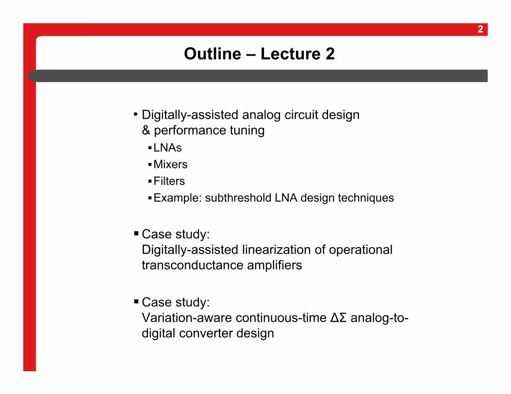
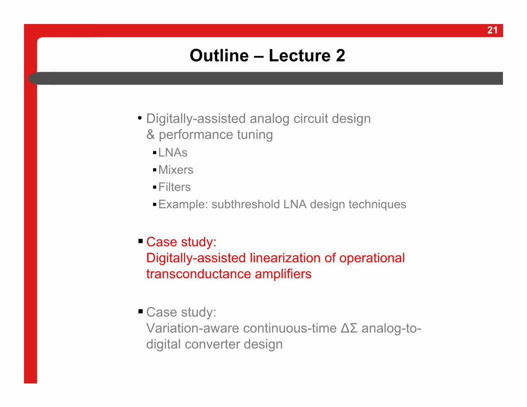
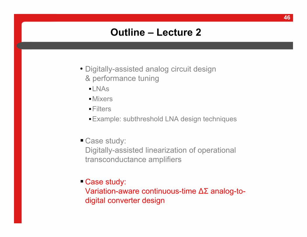
Outline – Lecture 2
• Digitally-assisted analog circuit design & performance tuningLNAsMixersFiltersExample: subthreshold LNA design techniques
Case study: Digitally-assisted linearization of operational transconductance amplifiers
Case study: Variation-aware continuous-time ∆Σ analog-to-digital converter design
3
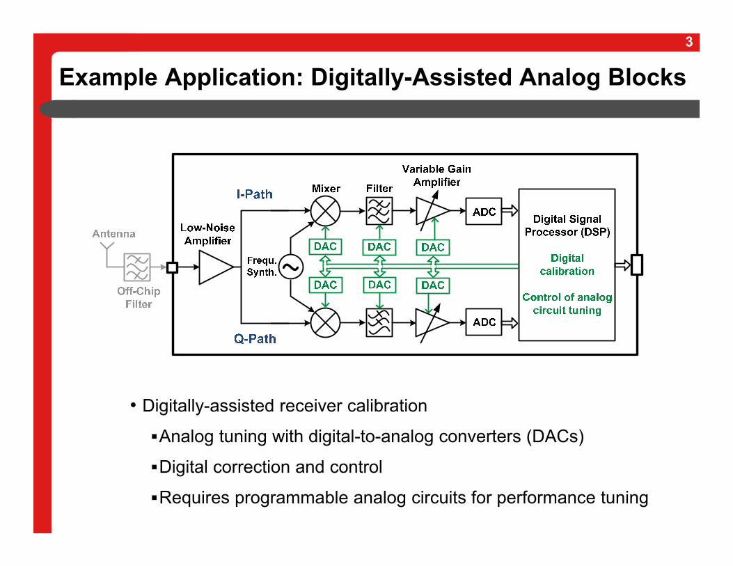
Example Application: Digitally-Assisted Analog Blocks
• Digitally-assisted receiver calibration
Analog tuning with digital-to-analog converters (DACs)
Digital correction and control
Requires programmable analog circuits for performance tuning
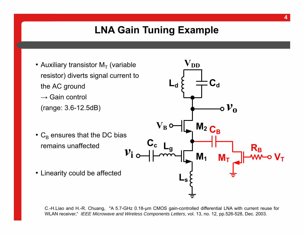
• Auxiliary transistor MT (variable resistor) diverts signal current to the AC ground → Gain control(range: 3.6-12.5dB)
• CB ensures that the DC bias remains unaffected
• Linearity could be affected
C.-H.Liao and H.-R. Chuang, "A 5.7-GHz 0.18-μm CMOS gain-controlled differential LNA with current reuse forWLAN receiver,“ IEEE Microwave and Wireless Components Letters, vol. 13, no. 12, pp.526-528, Dec. 2003.
1
2
d
B
DD
s
c
d
T
B
BT
g
4
LNA Gain Tuning Example
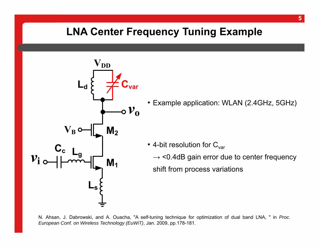
• Example application: WLAN (2.4GHz, 5GHz)
• 4-bit resolution for Cvar
→ <0.4dB gain error due to center frequency
shift from process variations
N. Ahsan, J. Dabrowski, and A. Ouacha, "A self-tuning technique for optimization of dual band LNA, " in Proc.European Conf. on Wireless Technology (EuWiT), Jan. 2009, pp.178-181.
1
2
d
B
DD
s
var
c g
5
LNA Center Frequency Tuning Example
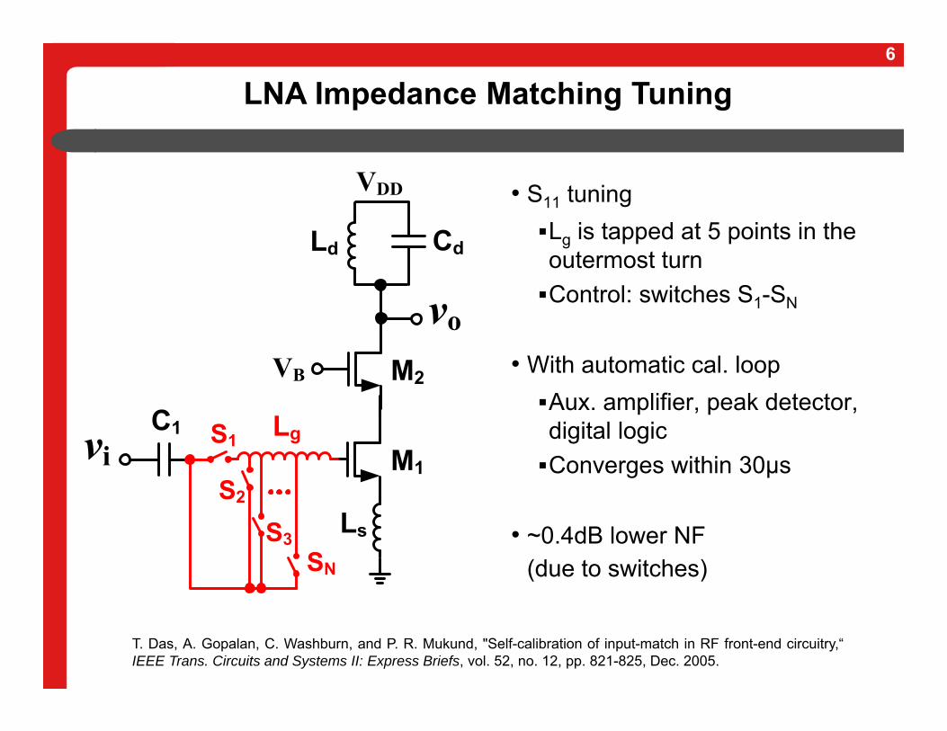
• S11 tuningLg is tapped at 5 points in the outermost turnControl: switches S1-SN
• With automatic cal. loopAux. amplifier, peak detector, digital logicConverges within 30μs
• ~0.4dB lower NF (due to switches)
T. Das, A. Gopalan, C. Washburn, and P. R. Mukund, "Self-calibration of input-match in RF front-end circuitry,“IEEE Trans. Circuits and Systems II: Express Briefs, vol. 52, no. 12, pp. 821-825, Dec. 2005.
1
2
d
B
DD
s
1
d
g
2
3
N
1
6
LNA Impedance Matching Tuning
Aux 2
R1Vb0
Vb1
Vo
Vdd
Cc
Vin M0
M1
Ib1
Vb2Ib2
MT
M2
R1
Vb3
MS
Ib3
Cc
Aux 1
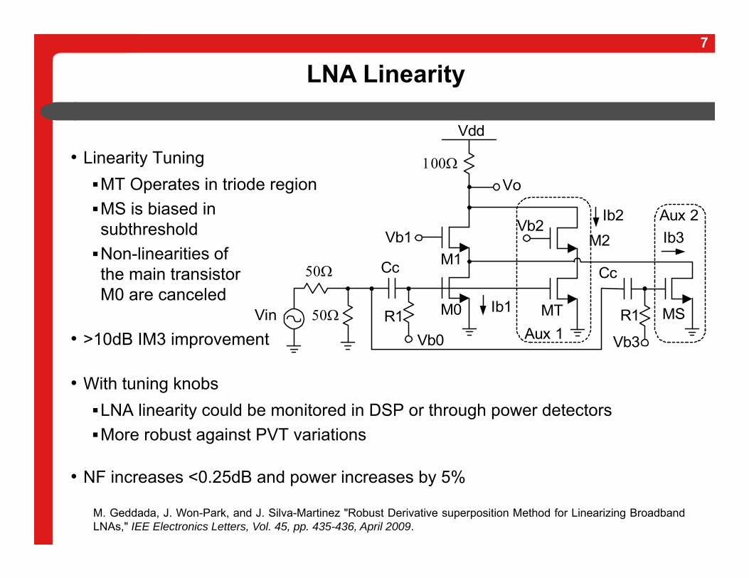
• Linearity TuningMT Operates in triode regionMS is biased in subthresholdNon-linearities ofthe main transistorM0 are canceled
• >10dB IM3 improvement
• With tuning knobsLNA linearity could be monitored in DSP or through power detectorsMore robust against PVT variations
• NF increases <0.25dB and power increases by 5%
M. Geddada, J. Won-Park, and J. Silva-Martinez "Robust Derivative superposition Method for Linearizing BroadbandLNAs," IEE Electronics Letters, Vol. 45, pp. 435-436, April 2009.
7
LNA Linearity
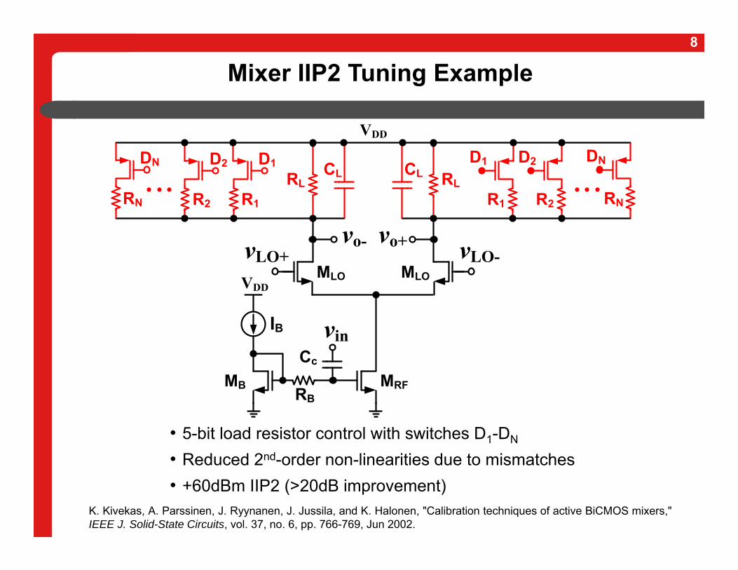
• 5-bit load resistor control with switches D1-DN
• Reduced 2nd-order non-linearities due to mismatches• +60dBm IIP2 (>20dB improvement)
K. Kivekas, A. Parssinen, J. Ryynanen, J. Jussila, and K. Halonen, "Calibration techniques of active BiCMOS mixers,"IEEE J. Solid-State Circuits, vol. 37, no. 6, pp. 766-769, Jun 2002.
MLO
RL
LO+
VDD
CL
o-
D1
R1
D2
R2
DN
RN
MRF
Cc
RB
in
MB
MLO
RL
LO-
CL
o+
D1
R1
D2
R2
DN
RN
B
VDD
8
Mixer IIP2 Tuning Example
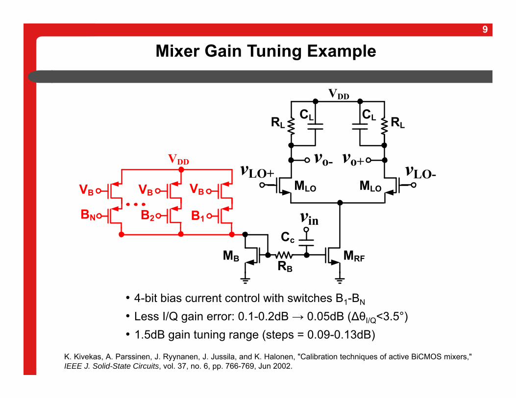
• 4-bit bias current control with switches B1-BN
• Less I/Q gain error: 0.1-0.2dB → 0.05dB (∆θI/Q<3.5°)• 1.5dB gain tuning range (steps = 0.09-0.13dB)
K. Kivekas, A. Parssinen, J. Ryynanen, J. Jussila, and K. Halonen, "Calibration techniques of active BiCMOS mixers,"IEEE J. Solid-State Circuits, vol. 37, no. 6, pp. 766-769, Jun 2002.
LO
L
DD
L
RF
c
BB
LO
LL
12N
DD
B B B
9
Mixer Gain Tuning Example
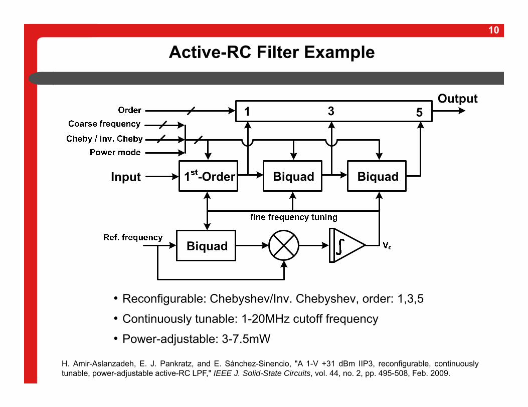
• Reconfigurable: Chebyshev/Inv. Chebyshev, order: 1,3,5
• Continuously tunable: 1-20MHz cutoff frequency
• Power-adjustable: 3-7.5mW
H. Amir-Aslanzadeh, E. J. Pankratz, and E. Sánchez-Sinencio, "A 1-V +31 dBm IIP3, reconfigurable, continuouslytunable, power-adjustable active-RC LPF," IEEE J. Solid-State Circuits, vol. 44, no. 2, pp. 495-508, Feb. 2009.
10
Active-RC Filter Example
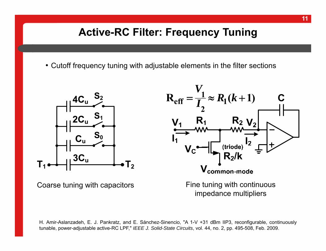
• Cutoff frequency tuning with adjustable elements in the filter sections
H. Amir-Aslanzadeh, E. J. Pankratz, and E. Sánchez-Sinencio, "A 1-V +31 dBm IIP3, reconfigurable, continuouslytunable, power-adjustable active-RC LPF," IEEE J. Solid-State Circuits, vol. 44, no. 2, pp. 495-508, Feb. 2009.
Coarse tuning with capacitors Fine tuning with continuous impedance multipliers
u
0u
1u
2u
1 2
)1(R 12
1eff kRI
V
11
Active-RC Filter: Frequency Tuning
Subthreshold Low-Noise Amplifier Design Techniques
Chun-hsiang ChangMarvin Onabajo
Northeastern University
13
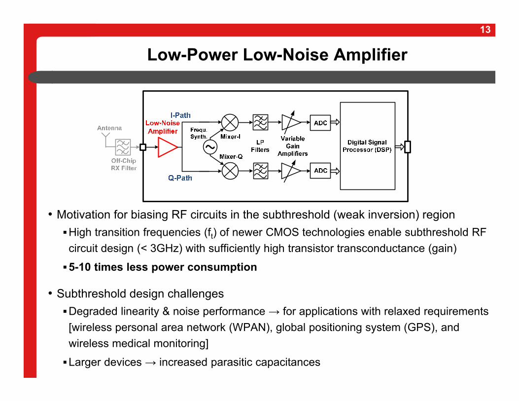
Low-Power Low-Noise Amplifier
• Motivation for biasing RF circuits in the subthreshold (weak inversion) regionHigh transition frequencies (ft) of newer CMOS technologies enable subthreshold RF circuit design (< 3GHz) with sufficiently high transistor transconductance (gain)
5-10 times less power consumption
• Subthreshold design challengesDegraded linearity & noise performance → for applications with relaxed requirements [wireless personal area network (WPAN), global positioning system (GPS), and wireless medical monitoring]
Larger devices → increased parasitic capacitances
14
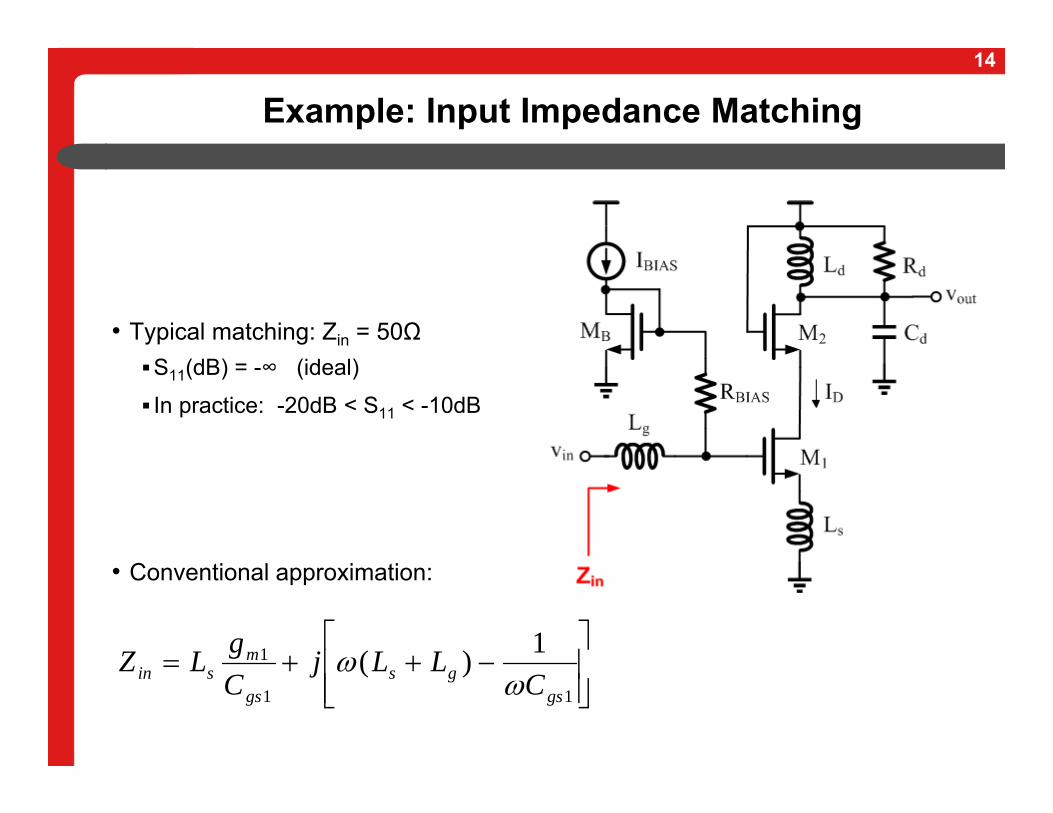
Example: Input Impedance Matching
• Typical matching: Zin = 50ΩS11(dB) = -∞ (ideal)
In practice: -20dB < S11 < -10dB
• Conventional approximation:
11
1 1)(gs
gsgs
msin C
LLjCgLZ
15
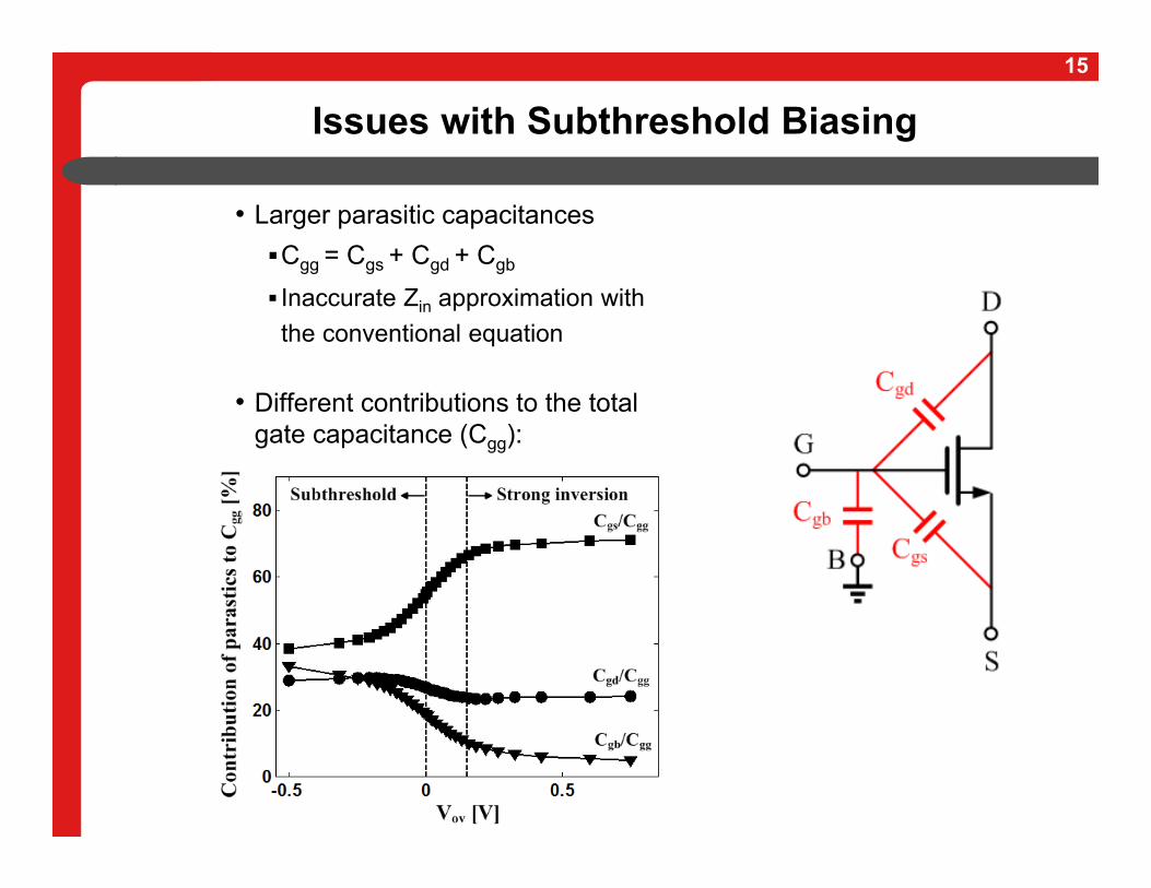
Issues with Subthreshold Biasing
• Larger parasitic capacitancesCgg = Cgs + Cgd + Cgb
Inaccurate Zin approximation with the conventional equation
• Different contributions to the totalgate capacitance (Cgg):
16
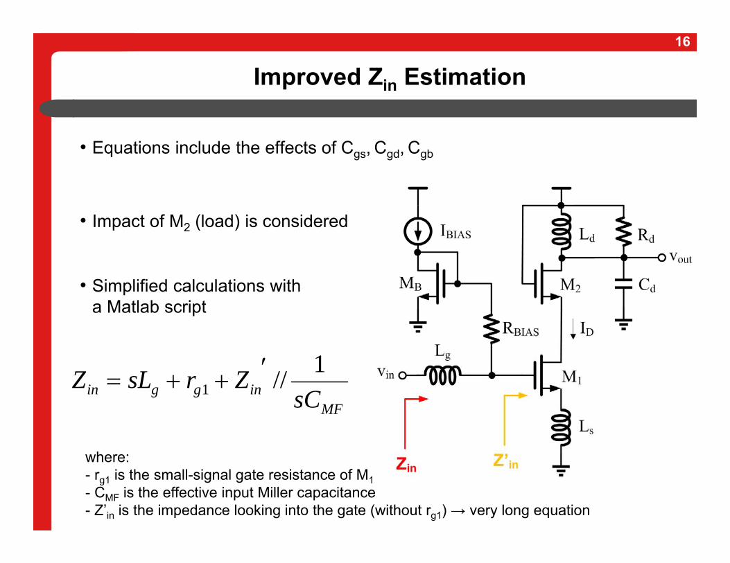
Improved Zin Estimation
• Equations include the effects of Cgs, Cgd, Cgb
• Impact of M2 (load) is considered
• Simplified calculations with a Matlab script
MFinggin sC
ZrsLZ 1//1
where:- rg1 is the small-signal gate resistance of M1- CMF is the effective input Miller capacitance- Z’in is the impedance looking into the gate (without rg1) → very long equation
17
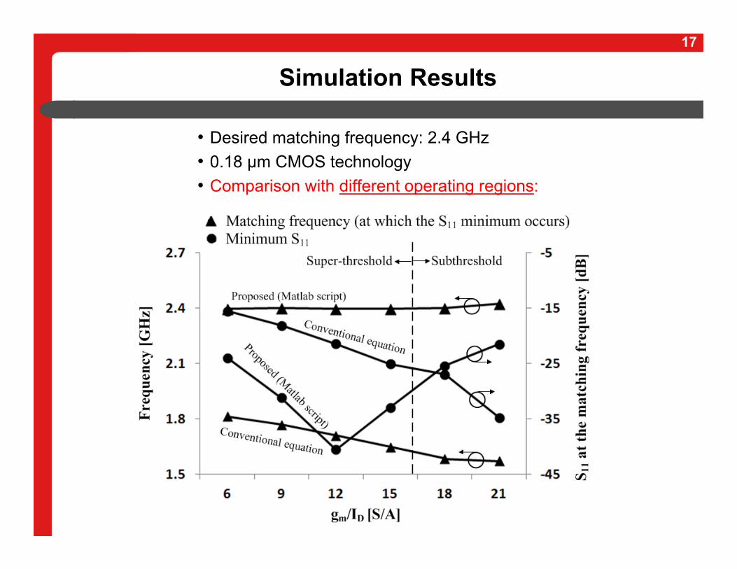
Simulation Results
• Desired matching frequency: 2.4 GHz• 0.18 µm CMOS technology• Comparison with different operating regions:
18
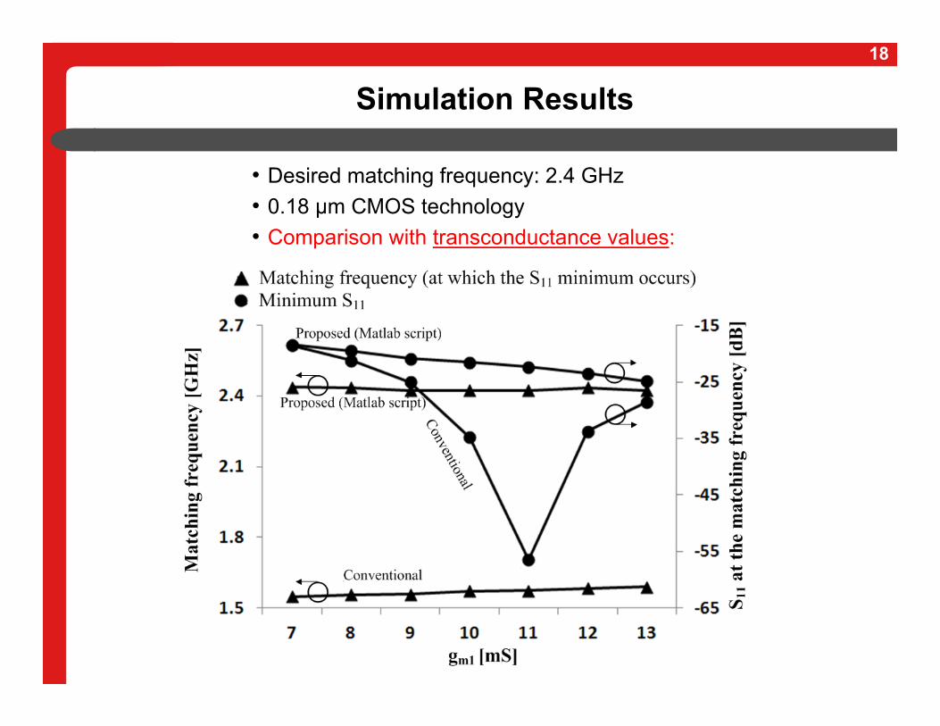
Simulation Results
• Desired matching frequency: 2.4 GHz• 0.18 µm CMOS technology• Comparison with transconductance values:
19
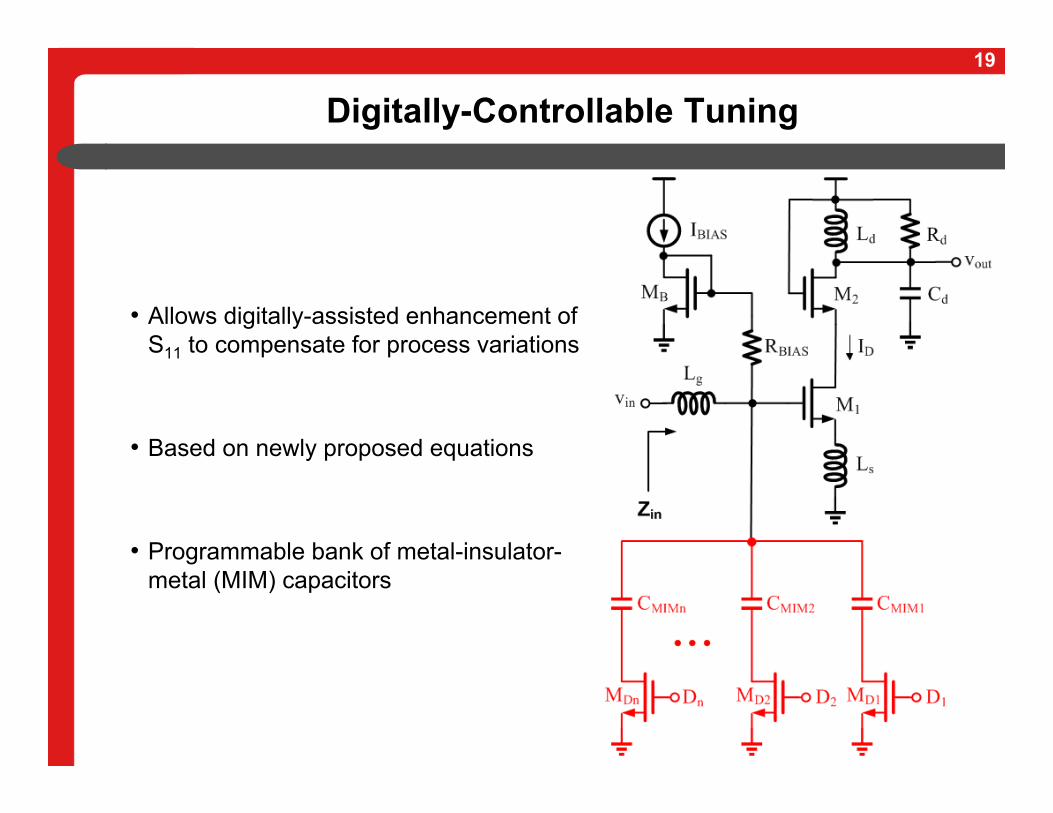
Digitally-Controllable Tuning
• Allows digitally-assisted enhancement of S11 to compensate for process variations
• Based on newly proposed equations
• Programmable bank of metal-insulator-metal (MIM) capacitors
20
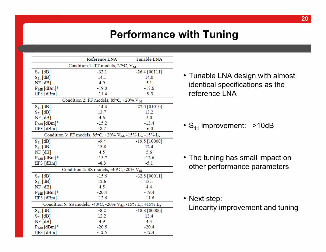
Performance with Tuning
• Tunable LNA design with almost identical specifications as the reference LNA
• S11 improvement: >10dB
• The tuning has small impact on other performance parameters
• Next step: Linearity improvement and tuning
21
Outline – Lecture 2
• Digitally-assisted analog circuit design & performance tuningLNAsMixersFiltersExample: subthreshold LNA design techniques
Case study: Digitally-assisted linearization of operational transconductance amplifiers
Case study: Variation-aware continuous-time ∆Σ analog-to-digital converter design
22
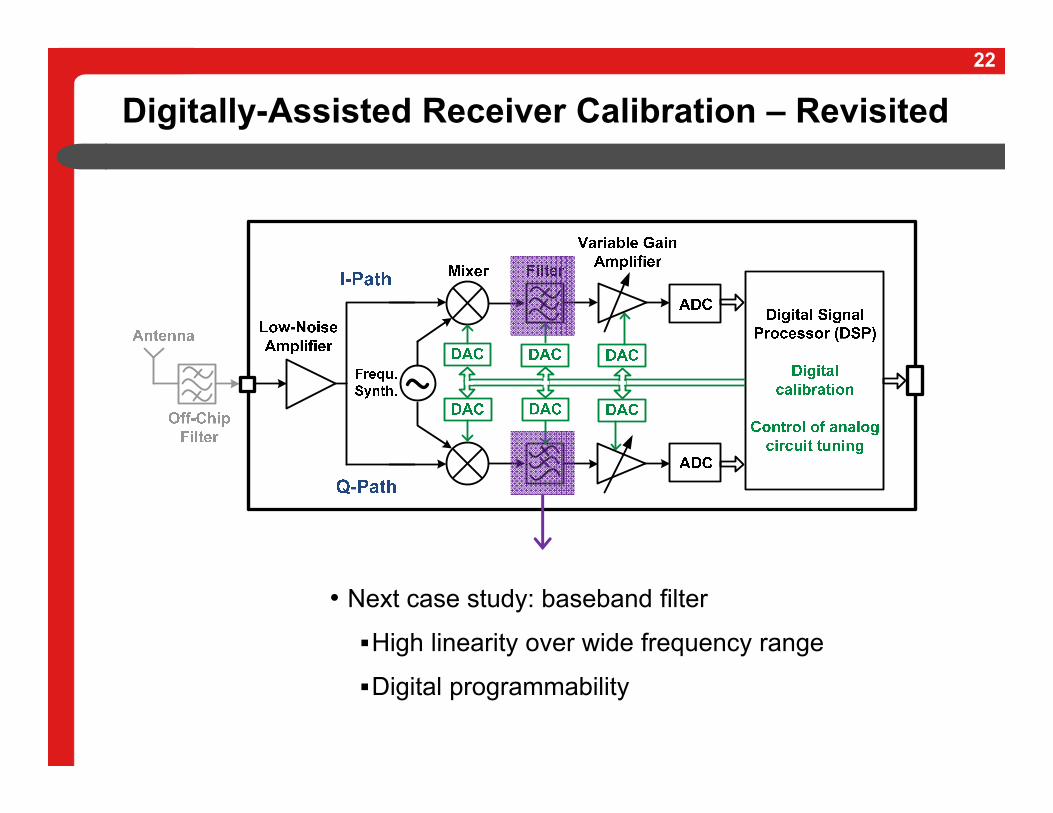
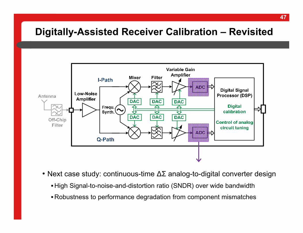
Digitally-Assisted Receiver Calibration – Revisited
• Next case study: baseband filter
High linearity over wide frequency range
Digital programmability
Operational Transconductance Amplifier Linearization
Team at Texas A&M University:
Mohamed MobarakMarvin Onabajo
Edgar Sánchez-SinencioJose Silva-Martinez
24
Motivation for OTA Linearization
• Applications with operational transconductance amplifiers (OTAs)On-chip filters in the 100-200MHz frequency rangeIn the intermediate frequency stage of wireless receiversContinuous-time Σ∆ analog-to-digital converters
Transconductance-capacitor baseband filtersBaseband frequency < 50MHz (ex. comm. standards: WiMAX, WLAN, WCDMA, UMTS)Third-order intermodulation distortion (IM3) < -60dB
• Project objectivesCancellation of OTA non-linearities (signal distortion reduction)Robustness of the linearization to process variationsCompensation for frequency-dependent linearity degradation
25
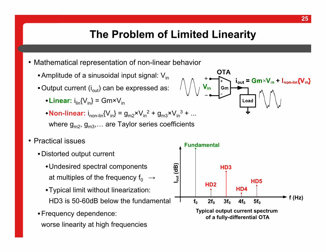
The Problem of Limited Linearity
• Mathematical representation of non-linear behavior
Amplitude of a sinusoidal input signal: Vin
Output current (iout) can be expressed as:
Linear: ilinVin = Gm×Vin
Non-linear: inon-linVin = gm2×Vin2 + gm3×Vin
3 + ... where gm2, gm3,… are Taylor series coefficients
• Practical issues
Distorted output current
Undesired spectral componentsat multiples of the frequency f0 →
Typical limit without linearization:HD3 is 50-60dB below the fundamental
Frequency dependence: worse linearity at high frequencies
Typical output current spectrum of a fully-differential OTA
Fundamental
f0 2f0 3f0 4f0 5f0f (Hz)
I out(d
B)
HD2
HD3
HD4HD5
26
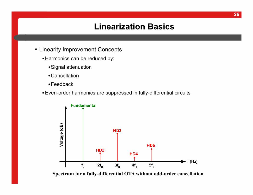
Linearization Basics
• Linearity Improvement ConceptsHarmonics can be reduced by:
Signal attenuation
Cancellation
Feedback
Even-order harmonics are suppressed in fully-differential circuits
Spectrum for a fully-differential OTA without odd-order cancellation
27
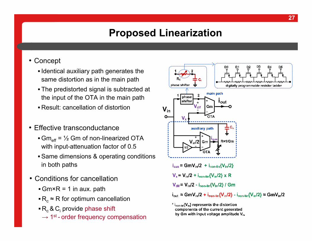
Proposed Linearization
• Concept Identical auxiliary path generates the
same distortion as in the main path The predistorted signal is subtracted at
the input of the OTA in the main pathResult: cancellation of distortion
• Effective transconductanceGmeff = ½ Gm of non-linearized OTA
with input-attenuation factor of 0.5Same dimensions & operating conditions
in both paths
• Conditions for cancellationGm×R = 1 in aux. pathRc ≈ R for optimum cancellationRc & Ci provide phase shift → 1st - order frequency compensation
28
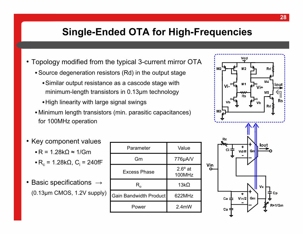
Single-Ended OTA for High-Frequencies
• Topology modified from the typical 3-current mirror OTASource degeneration resistors (Rd) in the output stage
Similar output resistance as a cascode stage with minimum-length transistors in 0.13μm technology
High linearity with large signal swings
Minimum length transistors (min. parasitic capacitances) for 100MHz operation
• Key component valuesR = 1.28kΩ ≈ 1/Gm
Rc = 1.28kΩ, Ci = 240fF
• Basic specifications →(0.13μm CMOS, 1.2V supply)
Parameter Value
Gm 776μA/V
Excess Phase 2.6º at100MHz
Ro 13kΩ
Gain Bandwidth Product 622MHz
Power 2.4mW
29
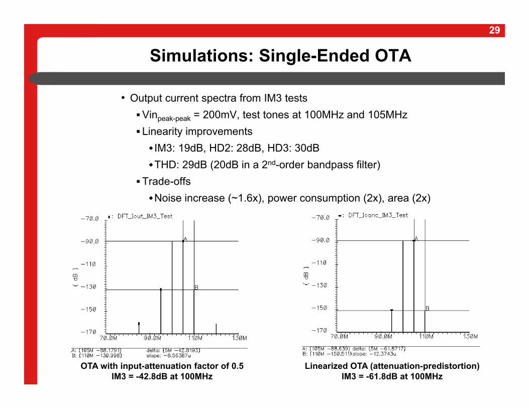
Simulations: Single-Ended OTA
• Output current spectra from IM3 testsVinpeak-peak = 200mV, test tones at 100MHz and 105MHzLinearity improvementsIM3: 19dB, HD2: 28dB, HD3: 30dBTHD: 29dB (20dB in a 2nd-order bandpass filter)
Trade-offsNoise increase (~1.6x), power consumption (2x), area (2x)
OTA with input-attenuation factor of 0.5IM3 = -42.8dB at 100MHz
Linearized OTA (attenuation-predistortion)IM3 = -61.8dB at 100MHz
30
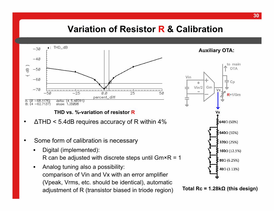
Variation of Resistor R & Calibration
• ∆THD < 5.4dB requires accuracy of R within 4%
• Some form of calibration is necessary Digital (implemented):
R can be adjusted with discrete steps until Gm×R = 1 Analog tuning also a possibility:
comparison of Vin and Vx with an error amplifier (Vpeak, Vrms, etc. should be identical), automatic adjustment of R (transistor biased in triode region) Total Rc = 1.28kΩ (this design)
THD vs. %-variation of resistor R
Auxiliary OTA:
31
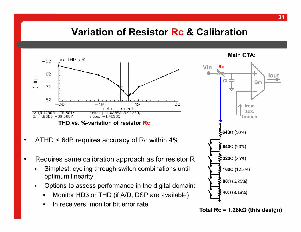
Variation of Resistor Rc & Calibration
• ∆THD < 6dB requires accuracy of Rc within 4%
• Requires same calibration approach as for resistor R Simplest: cycling through switch combinations until
optimum linearity Options to assess performance in the digital domain: Monitor HD3 or THD (if A/D, DSP are available) In receivers: monitor bit error rate
THD vs. %-variation of resistor Rc
Total Rc = 1.28kΩ (this design)
Main OTA:
Gm
VinIout
Ci
Rc
from aux.
branch
40Ω (3.13%)
80Ω (6.25%)
160Ω (12.5%)
320Ω (25%)
640Ω (50%)
640Ω (50%)
32
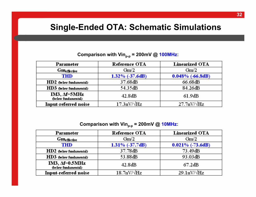
Single-Ended OTA: Schematic Simulations
Comparison with Vinp-p = 200mV @ 10MHz:
Comparison with Vinp-p = 200mV @ 100MHz:
33
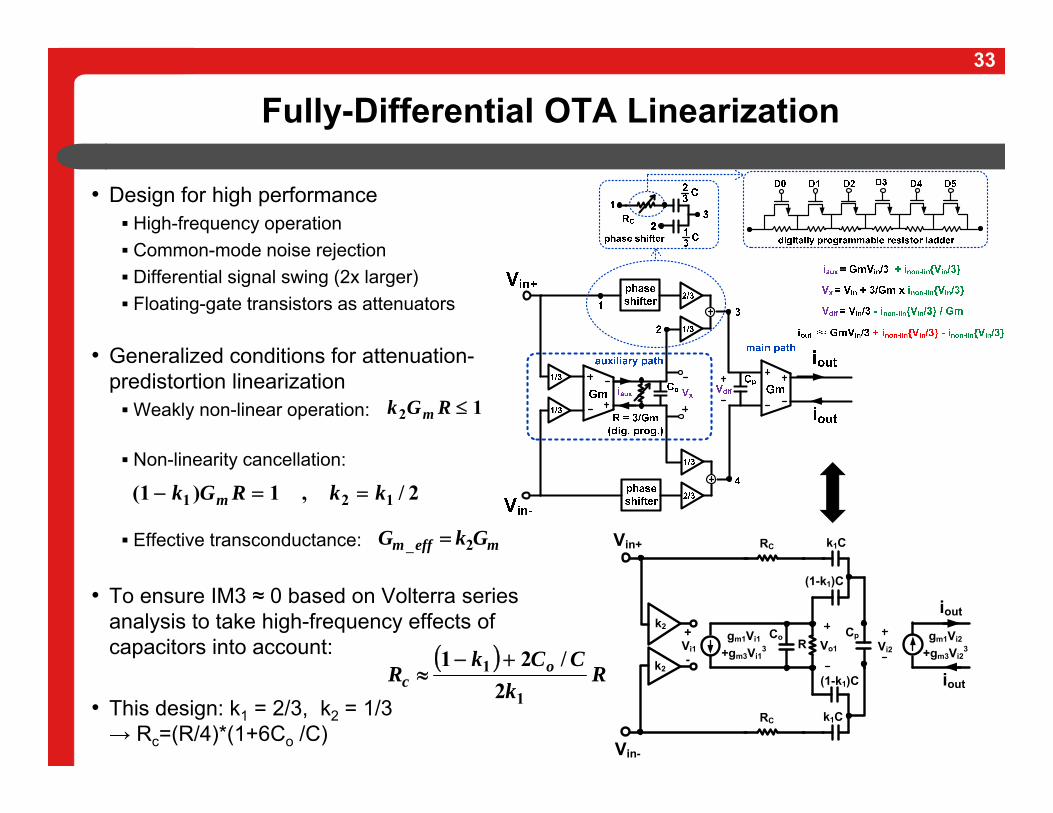
Fully-Differential OTA Linearization
• Design for high performance High-frequency operation Common-mode noise rejection Differential signal swing (2x larger) Floating-gate transistors as attenuators
• Generalized conditions for attenuation-predistortion linearizationWeakly non-linear operation:
Non-linearity cancellation:
Effective transconductance:
• To ensure IM3 ≈ 0 based on Volterra series analysis to take high-frequency effects of capacitors into account:
• This design: k1 = 2/3, k2 = 1/3→ Rc=(R/4)*(1+6Co /C)
k1CRC
(1-k1)C
Vin+
Vin-
k2
R
iout
Vi2Vi1
+
-
gm1Vi1
+gm3Vi13
k1CRC
(1-k1)C iout
Vo1
k2
gm1Vi2
+gm3Vi23
CpCo
R
kCCk
R oc
1
1
2/21
12 RGk m
2/,1)1( 121 kkRGk m
meffm GkG 2_
34
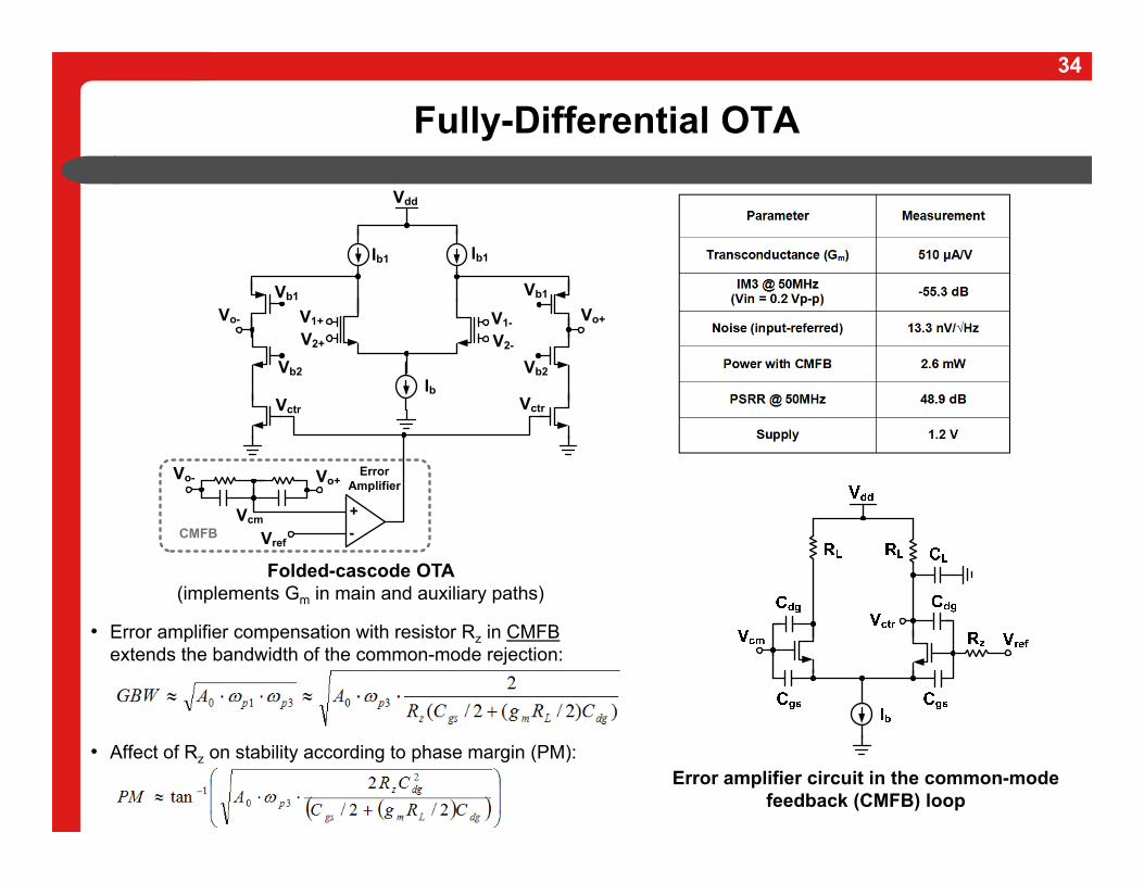
Fully-Differential OTA
• Error amplifier compensation with resistor Rz in CMFBextends the bandwidth of the common-mode rejection:
• Affect of Rz on stability according to phase margin (PM):
Folded-cascode OTA (implements Gm in main and auxiliary paths)
Error amplifier circuit in the common-mode feedback (CMFB) loop
Vb1
Vb2
Vctr
Vb1
Vb2
Vctr
V1+Vo- Vo+
Ib
Ib1 Ib1
+-
Vo+Vo-
Vref
ErrorAmplifier
Vdd
V2+
V1-
V2-
CMFBVcm
35
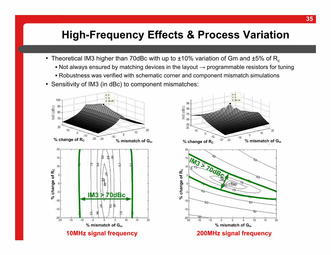
High-Frequency Effects & Process Variation
• Theoretical IM3 higher than 70dBc with up to ±10% variation of Gm and ±5% of Rc
Not always ensured by matching devices in the layout → programmable resistors for tuning Robustness was verified with schematic corner and component mismatch simulations
• Sensitivity of IM3 (in dBc) to component mismatches:
10MHz signal frequency 200MHz signal frequency

36
IM3 vs. change in Rc at 350MHzIM3 vs. R with 10% transconductance mismatchbetween main OTA and auxiliary OTA at 350MHz
Simulated Fully-Diff. OTA: Resistor Variations
• IM3 better than 71dBc for ±7.5% Rc-variation
• IM3 better than 71dBc for ±3.3% R-variation in the presence of 10% Gm-mismatch
• Reference OTA has IM3 of 51dBc
211
112
21
3
13
211
1111
2
211
11112
21
3
133
114/3
/212/
1211
12114/3
/212/
cbjRCkjVV
CCkg
cbjRCjRkRkCj
cbjRCjRkRkCjVV
CCkgi
cinin
pm
ococinin
pmIM
Theoretical IM3:
37
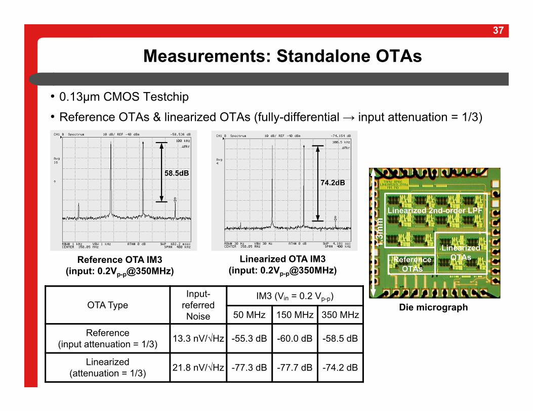
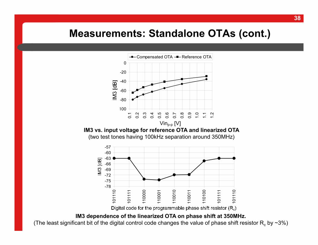
Measurements: Standalone OTAs
• 0.13μm CMOS Testchip
• Reference OTAs & linearized OTAs (fully-differential → input attenuation = 1/3)
Die micrograph
Reference OTA IM3(input: 0.2Vp-p@350MHz)
Linearized OTA IM3(input: 0.2Vp-p@350MHz)
OTA TypeInput-
referred Noise
IM3 (Vin = 0.2 Vp-p)
50 MHz 150 MHz 350 MHz
Reference(input attenuation = 1/3) 13.3 nV/√Hz -55.3 dB -60.0 dB -58.5 dB
Linearized(attenuation = 1/3) 21.8 nV/√Hz -77.3 dB -77.7 dB -74.2 dB
-78-75-72-69-66-63-60-57
1011
10
1011
11
1100
00
1100
01
1100
10
1100
11
1101
00
1011
11
1011
10
Digital code for the programmable phase shift resistor (Rc)
IM3
[dB
]
38
-100
-80
-60
-40
-20
0
0.1
0.2
0.3
0.4
0.5
0.6
0.7
0.8
0.9
1.0
1.1
1.2
Vin_peak-peak [V]
IM3
[dB
]
Compensated OTA Reference OTA
Vinp-p [V]
Measurements: Standalone OTAs (cont.)
IM3 vs. input voltage for reference OTA and linearized OTA (two test tones having 100kHz separation around 350MHz)
IM3 dependence of the linearized OTA on phase shift at 350MHz. (The least significant bit of the digital control code changes the value of phase shift resistor Rc by ~3%)
39
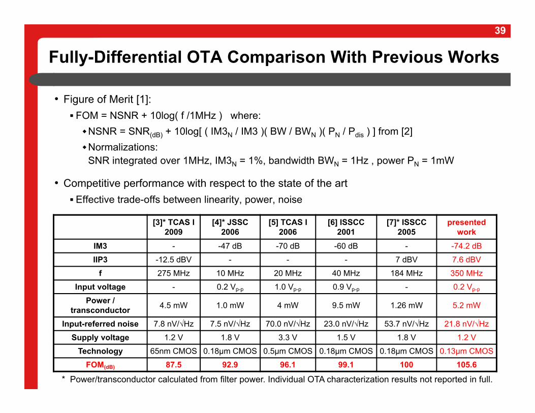
Fully-Differential OTA Comparison With Previous Works
• Figure of Merit [1]: FOM = NSNR + 10log( f /1MHz ) where:NSNR = SNR(dB) + 10log[ ( IM3N / IM3 )( BW / BWN )( PN / Pdis ) ] from [2]Normalizations:
SNR integrated over 1MHz, IM3N = 1%, bandwidth BWN = 1Hz , power PN = 1mW
• Competitive performance with respect to the state of the artEffective trade-offs between linearity, power, noise
[3]* TCAS I2009
[4]* JSSC2006
[5] TCAS I2006
[6] ISSCC2001
[7]* ISSCC2005
presented work
IM3 - -47 dB -70 dB -60 dB - -74.2 dB
IIP3 -12.5 dBV - - - 7 dBV 7.6 dBV
f 275 MHz 10 MHz 20 MHz 40 MHz 184 MHz 350 MHz
Input voltage - 0.2 Vp-p 1.0 Vp-p 0.9 Vp-p - 0.2 Vp-p
Power / transconductor 4.5 mW 1.0 mW 4 mW 9.5 mW 1.26 mW 5.2 mW
Input-referred noise 7.8 nV/√Hz 7.5 nV/√Hz 70.0 nV/√Hz 23.0 nV/√Hz 53.7 nV/√Hz 21.8 nV/√Hz
Supply voltage 1.2 V 1.8 V 3.3 V 1.5 V 1.8 V 1.2 V
Technology 65nm CMOS 0.18μm CMOS 0.5μm CMOS 0.18μm CMOS 0.18μm CMOS 0.13μm CMOS
FOM(dB) 87.5 92.9 96.1 99.1 100 105.6
* Power/transconductor calculated from filter power. Individual OTA characterization results not reported in full.
40
OTA Linearization References
• Cited on the previous slide:
[1] A. Lewinski and J. Silva-Martinez, “A high-frequency transconductor using a robust nonlinearitycancellation,” IEEE Trans. Circuits and Systems II: Express Briefs, vol. 53, no. 9, pp. 896-900, Sept. 2006.
[2] E. A. M. Klumperink and B. Nauta, “Systematic comparison of HF CMOS transconductors,” IEEE Trans.Circuits and Systems II: Express Briefs, vol. 50, no. 10, pp. 728-741, Oct. 2003.
[3] V. Saari, M. Kaltiokallio, S. Lindfors, J. Ryynänen, and K. A. I. Halonen, “A 240-MHz low-pass filter withvariable gain in 65-nm CMOS for a UWB radio receiver,” in IEEE Trans. Circuits and Systems I: RegularPapers, vol. 56, no. 7, pp. 1488–1499, Jul. 2009.
[4] S. D'Amico, M. Conta, and A. Baschirotto, "A 4.1-mW 10-MHz fourth-order source-follower-basedcontinuous-time filter with 79-dB DR," IEEE J. Solid-State Circuits, vol. 41, no. 12, pp. 2713-2719, Dec.2006.
[5] J. Chen, E. Sánchez-Sinencio, and J. Silva-Martinez, “Frequency-dependent harmonic-distortion analysis ofa linearized cross-coupled CMOS OTA and its application to OTA-C filters,” IEEE Trans. Circuits andSystems I: Regular Papers, vol. 53, no. 3, pp. 499-510, March 2006.
[6] D. Yongwang and R. Harjani, "A +18 dBm IIP3 LNA in 0.35μm CMOS," in ISSCC Dig. Tech. Papers,pp.162-163, Feb. 2001.
[7] J. C. Rudell, O. E. Erdogan, D. G. Yee, R. Brockenbrough, C. S. G. Conroy, and B. Kim, "A 5th-ordercontinuous-time harmonic-rejection GmC filter with in-situ calibration for use in transmitter applications," inISSCC Dig. Tech. Papers, pp. 322-323, Feb. 2005.
41
OTA Linearization without Increased Power
• Requires redesign of the OTA with 50% of the initial bias current Increased W/L ratio to maintain the same transconductance valueParasitic capacitances of the larger devices lead to bandwidh (f3dB) reductionGate-source overdrive (saturation) voltage is approximately 50% less
• Trade-off to maintain similar transconductance and +20dB linearity enhancement without power increase: Bandwidth reduction
• Example – Comparison after linearization (redesign of the fully-differential OTA)with the same power consumption as the non-linearized reference OTA:
OTA type VDSAT of input diff. pair
f3db with 50Ω load
Input-referred noise Power IM3
(Vin = 0.2 Vp-p)
Normalized |FOM|
(at fmax)
Reference (input attenuation = 1/3) 90 mV 2.49 GHz 9.7 nV/√Hz 2.6 mW
-53.1 dB atfmax = 350MHz
(-53.2 dB at 100MHz)
57.2
Linearized (attenuation = 1/3 & compensation)
54 mV 1.09 GHz 14.3 nV/√Hz 2.6 mW -77.1 dB atfmax = 100MHz 119.2
42
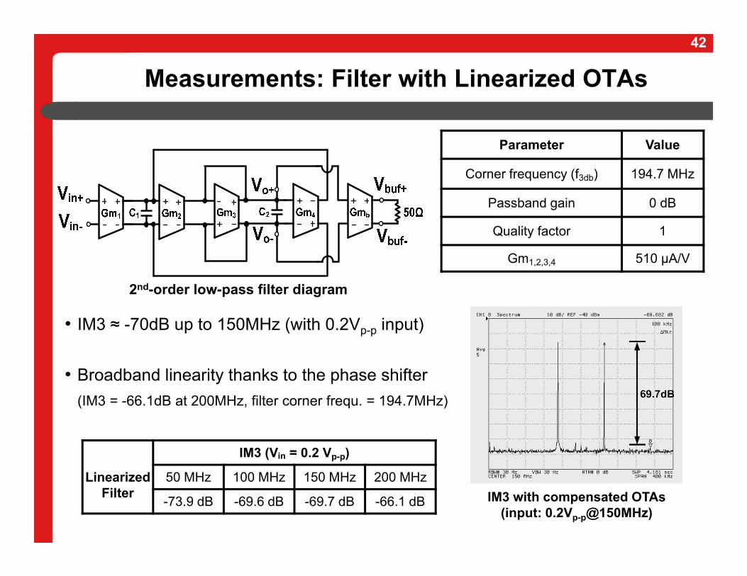
Measurements: Filter with Linearized OTAs
• IM3 ≈ -70dB up to 150MHz (with 0.2Vp-p input)
• Broadband linearity thanks to the phase shifter (IM3 = -66.1dB at 200MHz, filter corner frequ. = 194.7MHz)
2nd-order low-pass filter diagram
IM3 with compensated OTAs (input: 0.2Vp-p@150MHz)
LinearizedFilter
IM3 (Vin = 0.2 Vp-p)
50 MHz 100 MHz 150 MHz 200 MHz
-73.9 dB -69.6 dB -69.7 dB -66.1 dB
Parameter Value
Corner frequency (f3db) 194.7 MHz
Passband gain 0 dB
Quality factor 1
Gm1,2,3,4 510 μA/V
43
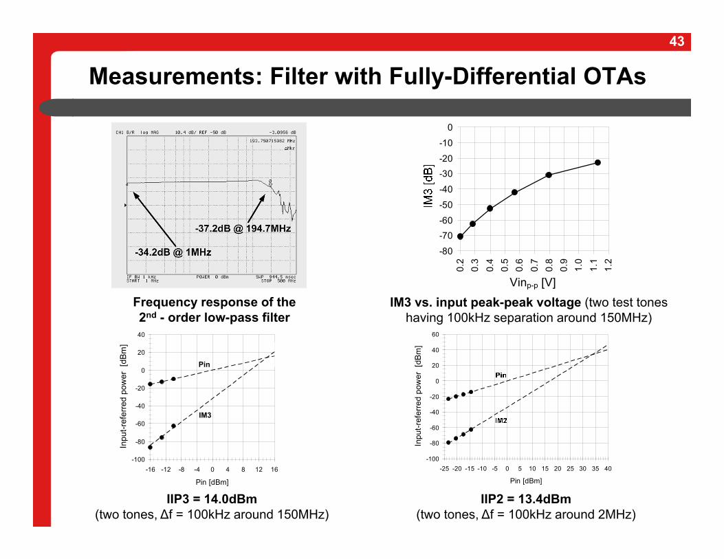
Measurements: Filter with Fully-Differential OTAs
Frequency response of the2nd - order low-pass filter
-80
-70-60
-50
-40
-30-20
-10
0
0.2
0.3
0.4
0.5
0.6
0.7
0.8
0.9
1.0
1.1
1.2
Vin_peak-peak [V]
IM3
[dB
]
Vinp-p [V]
IM3 vs. input peak-peak voltage (two test tones having 100kHz separation around 150MHz)
-100
-80
-60
-40
-20
0
20
40
-16 -12 -8 -4 0 4 8 12 16
Pin [dBm]
Inpu
t-ref
erre
d po
wer
[dB
m]
Pin
IM3
-100
-80
-60
-40
-20
0
20
40
60
-25 -20 -15 -10 -5 0 5 10 15 20 25 30 35 40
Pin [dBm]
Inpu
t-ref
erre
d po
wer
[dB
m]
IIP3 = 14.0dBm (two tones, ∆f = 100kHz around 150MHz)
IIP2 = 13.4dBm(two tones, ∆f = 100kHz around 2MHz)
44
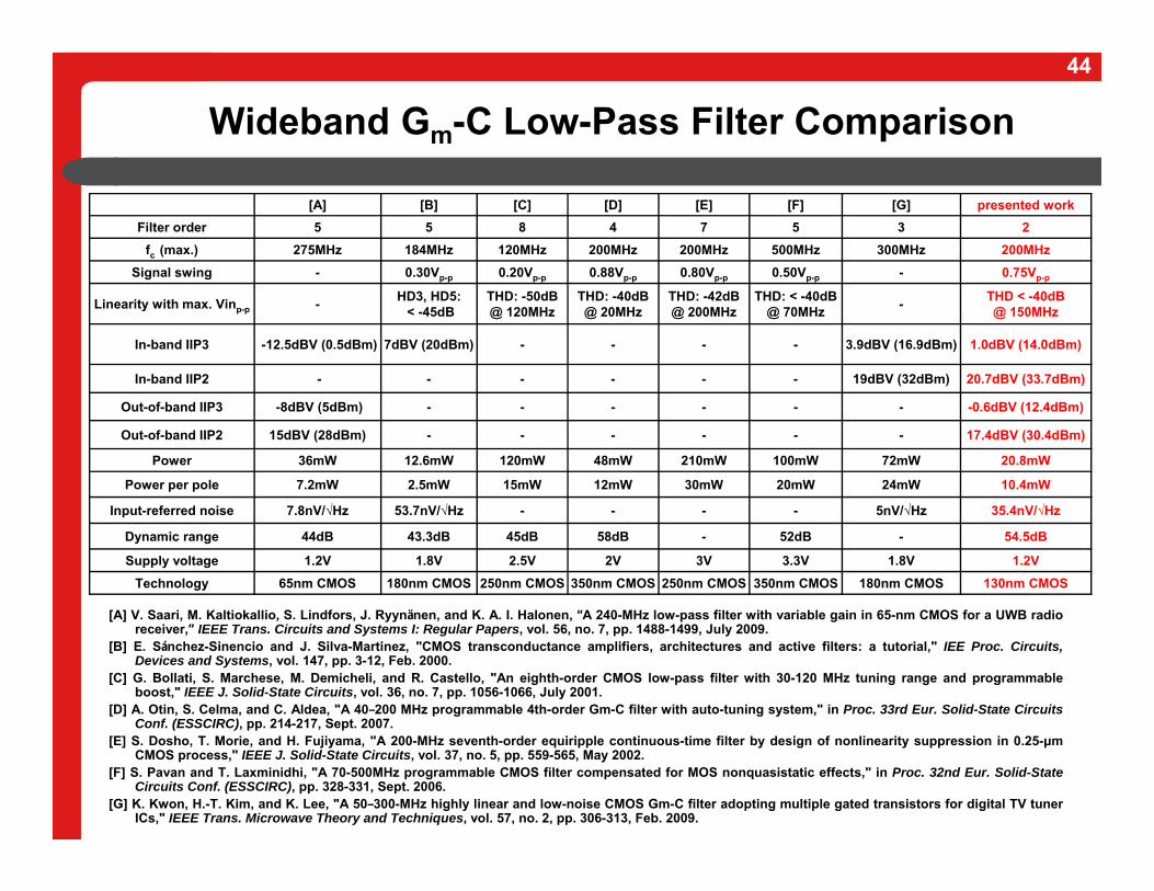
Wideband Gm-C Low-Pass Filter Comparison
[A] V. Saari, M. Kaltiokallio, S. Lindfors, J. Ryynänen, and K. A. I. Halonen, “A 240-MHz low-pass filter with variable gain in 65-nm CMOS for a UWB radioreceiver,” IEEE Trans. Circuits and Systems I: Regular Papers, vol. 56, no. 7, pp. 1488-1499, July 2009.
[B] E. Sánchez-Sinencio and J. Silva-Martinez, "CMOS transconductance amplifiers, architectures and active filters: a tutorial," IEE Proc. Circuits,Devices and Systems, vol. 147, pp. 3-12, Feb. 2000.
[C] G. Bollati, S. Marchese, M. Demicheli, and R. Castello, "An eighth-order CMOS low-pass filter with 30-120 MHz tuning range and programmableboost," IEEE J. Solid-State Circuits, vol. 36, no. 7, pp. 1056-1066, July 2001.
[D] A. Otin, S. Celma, and C. Aldea, "A 40–200 MHz programmable 4th-order Gm-C filter with auto-tuning system," in Proc. 33rd Eur. Solid-State CircuitsConf. (ESSCIRC), pp. 214-217, Sept. 2007.
[E] S. Dosho, T. Morie, and H. Fujiyama, "A 200-MHz seventh-order equiripple continuous-time filter by design of nonlinearity suppression in 0.25-μmCMOS process," IEEE J. Solid-State Circuits, vol. 37, no. 5, pp. 559-565, May 2002.
[F] S. Pavan and T. Laxminidhi, "A 70-500MHz programmable CMOS filter compensated for MOS nonquasistatic effects," in Proc. 32nd Eur. Solid-StateCircuits Conf. (ESSCIRC), pp. 328-331, Sept. 2006.
[G] K. Kwon, H.-T. Kim, and K. Lee, "A 50–300-MHz highly linear and low-noise CMOS Gm-C filter adopting multiple gated transistors for digital TV tunerICs," IEEE Trans. Microwave Theory and Techniques, vol. 57, no. 2, pp. 306-313, Feb. 2009.
[A] [B] [C] [D] [E] [F] [G] presented workFilter order 5 5 8 4 7 5 3 2
fc (max.) 275MHz 184MHz 120MHz 200MHz 200MHz 500MHz 300MHz 200MHzSignal swing - 0.30Vp-p 0.20Vp-p 0.88Vp-p 0.80Vp-p 0.50Vp-p - 0.75Vp-p
Linearity with max. Vinp-p - HD3, HD5: < -45dB
THD: -50dB @ 120MHz
THD: -40dB @ 20MHz
THD: -42dB @ 200MHz
THD: < -40dB @ 70MHz - THD < -40dB
@ 150MHz
In-band IIP3 -12.5dBV (0.5dBm) 7dBV (20dBm) - - - - 3.9dBV (16.9dBm) 1.0dBV (14.0dBm)
In-band IIP2 - - - - - - 19dBV (32dBm) 20.7dBV (33.7dBm)
Out-of-band IIP3 -8dBV (5dBm) - - - - - - -0.6dBV (12.4dBm)
Out-of-band IIP2 15dBV (28dBm) - - - - - - 17.4dBV (30.4dBm)
Power 36mW 12.6mW 120mW 48mW 210mW 100mW 72mW 20.8mW
Power per pole 7.2mW 2.5mW 15mW 12mW 30mW 20mW 24mW 10.4mW
Input-referred noise 7.8nV/√Hz 53.7nV/√Hz - - - - 5nV/√Hz 35.4nV/√Hz
Dynamic range 44dB 43.3dB 45dB 58dB - 52dB - 54.5dB
Supply voltage 1.2V 1.8V 2.5V 2V 3V 3.3V 1.8V 1.2VTechnology 65nm CMOS 180nm CMOS 250nm CMOS 350nm CMOS 250nm CMOS 350nm CMOS 180nm CMOS 130nm CMOS
45
OTA Linearization: Summary & Conclusions
• Proposed linearization techniqueFor OTAs in transconductance-C filter applications
Independent of the OTA circuit topology
Allows linearity, noise, power design trade-offs
• Measured performance IM3 improvement of up to 22dB
Performance meets state-of-the-art requirements
• Compensation for PVT variations and high-frequency effectsBased on digital adjustment of resistors
Main amplifier can be optimized for its target application(no internal circuit design change due to the linearization scheme)
M. Mobarak, M. Onabajo, J. Silva-Martinez, and E. Sánchez-Sinencio, “Attenuation-predistortion linearization ofCMOS OTAs with digital correction of process variations in OTA-C filter applications,” IEEE J. Solid-State Circuits, vol.45, no. 2, pp. 351-367, Feb. 2010.
46
Outline – Lecture 2
• Digitally-assisted analog circuit design & performance tuningLNAsMixersFiltersExample: subthreshold LNA design techniques
Case study: Digitally-assisted linearization of operational transconductance amplifiers
Case study: Variation-aware continuous-time ∆Σ analog-to-digital converter design
47
Digitally-Assisted Receiver Calibration – Revisited
• Next case study: continuous-time ∆Σ analog-to-digital converter designHigh Signal-to-noise-and-distortion ratio (SNDR) over wide bandwidth
Robustness to performance degradation from component mismatches
Variation-Aware Continuous-Time ∆Σ Analog-to-Digital Converter Design
Team at Texas A&M University:
Cho-Ying Lu, Marvin Onabajo, Venkata Gadde, Yung-Chung Lo, Hsien-Pu Chen, Vijay Periasamy,
Jose Silva-Martinez
49
Specific Quantizer Application Overview
• Analog-to-digital converter (ADC) group projectContinuous-time low-pass Σ∆ modulator with competitive specifications
25MHz bandwidth, sampling frequency = 400MHz
Signal-to-noise-and-distortion ratio (SNDR) = 67.7dB
Power consumption = 48mW
Robustness to performance degradation from component mismatches
Device mismatches → non-linearities (signal distortion) → SNDR degradation
Novel multi-bit feedback with a single-element digital-analog-converter (DAC)using pulse width modulation (PWM)→ Avoids non-linearities from unit element mismatches
(encountered in conventional multi-bit DACs)
• Presentation focus: 3-bit quantizerProposed topology is optimized for the PWM DAC approach (multiple clock phases)
Option for adjusting quantization levels to compensate for process variations
50
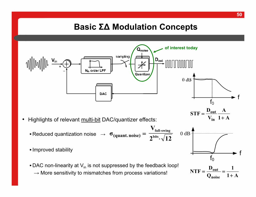
Basic Σ∆ Modulation Concepts
0
0 dB
A11
QDNTF
noise
out
A1A
VDSTF
in
out
• Highlights of relevant multi-bit DAC/quantizer effects:
Reduced quantization noise →
Improved stability
DAC non-linearity at Vin is not suppressed by the feedback loop!→ More sensitivity to mismatches from process variations!
of interest today
noise) (quant.σ122
Vbits
-swingfull
51
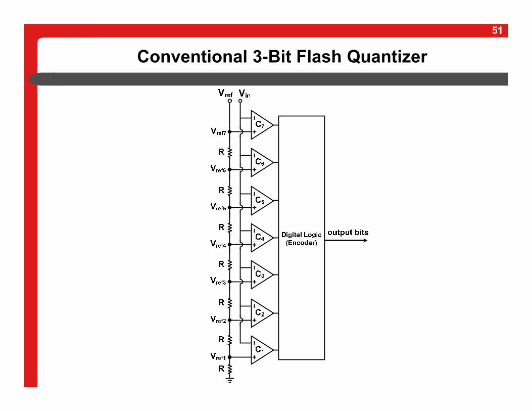
Conventional 3-Bit Flash Quantizer
52
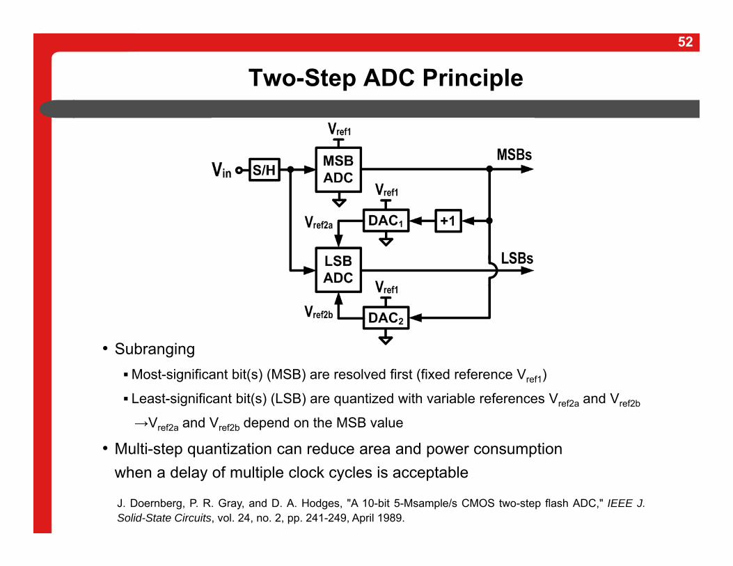
Two-Step ADC Principle
J. Doernberg, P. R. Gray, and D. A. Hodges, "A 10-bit 5-Msample/s CMOS two-step flash ADC," IEEE J.Solid-State Circuits, vol. 24, no. 2, pp. 241-249, April 1989.
• SubrangingMost-significant bit(s) (MSB) are resolved first (fixed reference Vref1)
Least-significant bit(s) (LSB) are quantized with variable references Vref2a and Vref2b
→Vref2a and Vref2b depend on the MSB value
• Multi-step quantization can reduce area and power consumption when a delay of multiple clock cycles is acceptable
53
Modern “Flash-like” ADC Examples
• Alternative architectures take advantage of technology scaling (fast switching)Enhanced performance at higher conversion speedsReduced power consumption Improving compatibility with digital CMOS processes
• Folding flash ADCComprised of 16 instead of 31 (conventional flash) comparators for 5-bit resolution 1.75 GS/s in 90nm CMOS, 2.2mW, 5-bit res.B. Verbruggen, J. Craninckx, M. Kuijk, P. Wambacq, and G. Van der Plas, "A 2.2 mW 1.75 GS/s 5 bit folding flash ADC in 90 nm digital CMOS," IEEE J. Solid-State Circuits, vol. 44, no. 3, pp.874-882, March 2009.
• Asynchronous ADCAsynchronous successive approximations performed with a single comparator Input is weighted against a reference that is changed with a switchable capacitor array 600-MS/s in 0.13µm CMOS, 5.3-mWS.-W. Chen and R. W. Brodersen, "A 6-bit 600-MS/s 5.3-mW asynchronous ADC in 0.13-μm CMOS," IEEE J. Solid-State Circuits, vol. 41, no. 12, pp. 2669-2680, Dec. 2006.
54
More Modern “Flash-like” ADC Examples
• Two-step ADC MSB is quantized first LSBs are determined with an asynchronous binary-search procedure 150MS/s in 90nm CMOS, 133µW, 7-bit res.G. Van der Plas and B. Verbruggen, "A 150MS/s 133μW 7b ADC in 90nm digital CMOS using a comparator-based asynchronous binary-search sub-ADC," in IEEE Intl. Solid-State Circuits Conf. (ISSCC) Dig. Tech. Papers, Feb. 2008, pp. 242-243, 610.
• Other related references:
J. Craninckx and G. Van der Plas, "A 65fJ/conversion-step 0-to-50MS/s 0-to-0.7mW 9b charge-sharing SAR ADC in 90nm digital CMOS," in IEEE Intl. Solid-State Circuits Conf. (ISSCC) Dig. Tech. Papers, Feb. 2007, pp. 246-247, 600.
L. Dorrer, F. Kuttner, P. Greco, P. Torta, and T. Hartig, "A 3-mW 74-dB SNR 2-MHz continuous-time delta-sigma ADC with a tracking ADC quantizer in 0.13-μm CMOS," IEEE J. Solid-State Circuits, vol. 40, no. 12, pp. 2416- 2427, Dec. 2005.
55
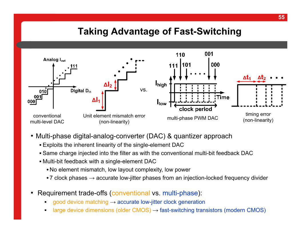
Taking Advantage of Fast-Switching
conventional multi-level DAC
Unit element mismatch error (non-linearity)
vs.
multi-phase PWM DACtiming error
(non-linearity)
∆I1
∆I2
• Requirement trade-offs (conventional vs. multi-phase): good device matching → accurate low-jitter clock generation large device dimensions (older CMOS) → fast-switching transistors (modern CMOS)
• Multi-phase digital-analog-converter (DAC) & quantizer approachExploits the inherent linearity of the single-element DACSame charge injected into the filter as with the conventional multi-bit feedback DACMulti-bit feedback with a single-element DACNo element mismatch, low layout complexity, low power7 clock phases → accurate low-jitter phases from an injection-locked frequency divider
56
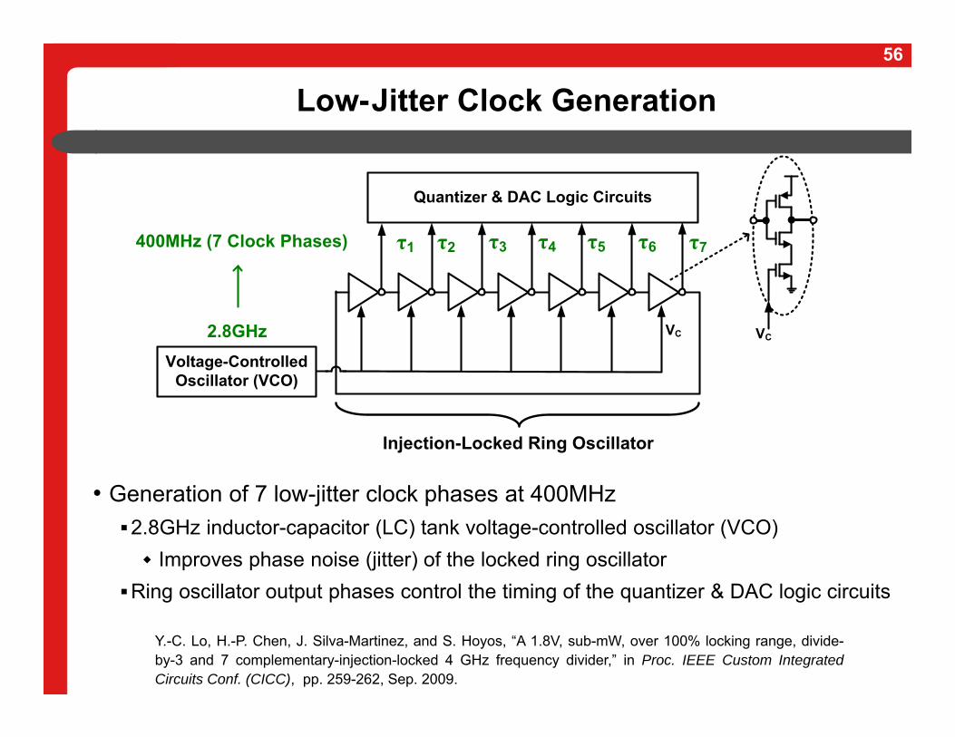
Low-Jitter Clock Generation
• Generation of 7 low-jitter clock phases at 400MHz2.8GHz inductor-capacitor (LC) tank voltage-controlled oscillator (VCO) Improves phase noise (jitter) of the locked ring oscillator
Ring oscillator output phases control the timing of the quantizer & DAC logic circuits
Voltage-Controlled Oscillator (VCO)
2.8GHz
τ1 τ2 τ3 τ4 τ5 τ6 τ7
Injection-Locked Ring Oscillator
400MHz (7 Clock Phases)
Quantizer & DAC Logic Circuits
VC VC
Y.-C. Lo, H.-P. Chen, J. Silva-Martinez, and S. Hoyos, “A 1.8V, sub-mW, over 100% locking range, divide-by-3 and 7 complementary-injection-locked 4 GHz frequency divider,” in Proc. IEEE Custom IntegratedCircuits Conf. (CICC), pp. 259-262, Sep. 2009.
57
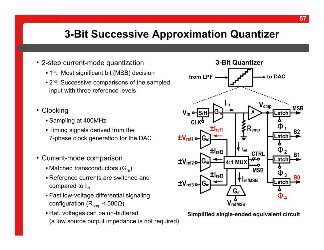
3-Bit Successive Approximation Quantizer
• 2-step current-mode quantization 1st: Most significant bit (MSB) decision 2nd: Successive comparisons of the sampled
input with three reference levels
• ClockingSampling at 400MHz Timing signals derived from the
7-phase clock generation for the DAC
• Current-mode comparisonMatched transconductors (Gm)Reference currents are switched and
compared to Iin Fast low-voltage differential signaling
configuration (Rcmp < 500Ω) Ref. voltages can be un-buffered
(a low source output impedance is not required)Simplified single-ended equivalent circuit
58
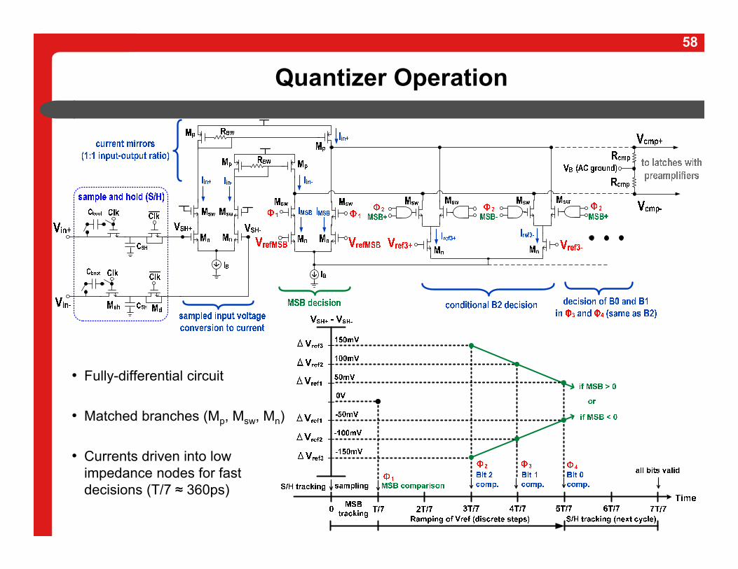
Quantizer Operation
• Fully-differential circuit
• Matched branches (Mp, Msw, Mn)
• Currents driven into low impedance nodes for fast decisions (T/7 ≈ 360ps)
59
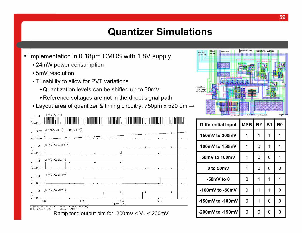
Quantizer Simulations
• Implementation in 0.18μm CMOS with 1.8V supply 24mW power consumption 5mV resolution Tunability to allow for PVT variationsQuantization levels can be shifted up to 30mVReference voltages are not in the direct signal path
Layout area of quantizer & timing circuitry: 750μm x 520 μm →
Differential Input MSB B2 B1 B0
150mV to 200mV 1 1 1 1
100mV to 150mV 1 0 1 1
50mV to 100mV 1 0 0 1
0 to 50mV 1 0 0 0
-50mV to 0 0 1 1 1
-100mV to -50mV 0 1 1 0
-150mV to -100mV 0 1 0 0
-200mV to -150mV 0 0 0 0Ramp test: output bits for -200mV < Vin < 200mV
60
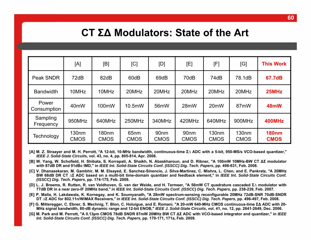
CT Σ∆ Modulators: State of the Art
[A] [B] [C] [D] [E] [F] [G] This Work
Peak SNDR 72dB 82dB 60dB 69dB 70dB 74dB 78.1dB 67.7dB
Bandwidth 10MHz 10MHz 20MHz 20MHz 20MHz 20MHz 20MHz 25MHz
PowerConsumption 40mW 100mW 10.5mW 56mW 28mW 20mW 87mW 48mW
SamplingFrequency 950MHz 640MHz 250MHz 340MHz 420MHz 640MHz 900MHz 400MHz
Technology 130nmCMOS
180nmCMOS
65nmCMOS
90nmCMOS
90nmCMOS
130nmCMOS
130nmCMOS
180nmCMOS
[A] M. Z. Straayer and M. H. Perrott, “A 12-bit, 10-MHz bandwidth, continuous-time Σ∆ ADC with a 5-bit, 950-MS/s VCO-based quantizer,”IEEE J. Solid-State Circuits, vol. 43, no. 4, pp. 805-814, Apr. 2008.
[B] W. Yang, W. Schofield, H. Shibata, S. Korrapati, A. Shaikh, N. Abaskharoun, and D. Ribner, "A 100mW 10MHz-BW CT ∆Σ modulatorwith 87dB DR and 91dBc IMD," in IEEE Int. Solid-State Circuits Conf. (ISSCC) Dig. Tech. Papers, pp. 498-631, Feb. 2008.
[C] V. Dhanasekaran, M. Gambhir, M. M. Elsayed, E. Sanchez-Sinencio, J. Silva-Martinez, C. Mishra, L. Chen, and E. Pankratz, “A 20MHzBW 68dB DR CT ∆Σ ADC based on a multi-bit time-domain quantizer and feedback element,” in IEEE Int. Solid-State Circuits Conf.(ISSCC) Dig. Tech. Papers, pp. 174-175, Feb. 2009.
[D] L. J. Breems, R. Rutten, R. van Veldhoven, G. van der Weide, and H. Termeer, “A 56mW CT quadrature cascaded Σ∆ modulator with77dB DR in a near zero-IF 20MHz band,” in IEEE Int. Solid-State Circuits Conf. (ISSCC) Dig. Tech. Papers, pp. 238-239, Feb. 2007.
[E] P. Malla, H. Lakdawala, K. Kornegay, and K. Soumyanath, “A 28mW spectrum-sensing reconfigurable 20MHz 72dB-SNR 70dB-SNDRDT ∆Σ ADC for 802.11n/WiMAX Receivers,” in IEEE Int. Solid-State Circuits Conf. (ISSCC) Dig. Tech. Papers, pp. 496-497, Feb. 2008.
[F] G. Mitteregger, C. Ebner, S. Mechnig, T. Blon, C. Holuigue, and E. Romani, "A 20-mW 640-MHz CMOS continuous-time Σ∆ ADC with 20-MHz signal bandwidth, 80-dB dynamic range and 12-bit ENOB," IEEE J. Solid-State Circuits, vol. 41, no. 12, pp. 2641-2649, Dec. 2006.
[G] M. Park and M. Perrott, "A 0.13µm CMOS 78dB SNDR 87mW 20MHz BW CT ∆Σ ADC with VCO-based integrator and quantizer," in IEEEInt. Solid-State Circuits Conf. (ISSCC) Dig. Tech. Papers, pp. 170-171, 171a, Feb. 2009.
61
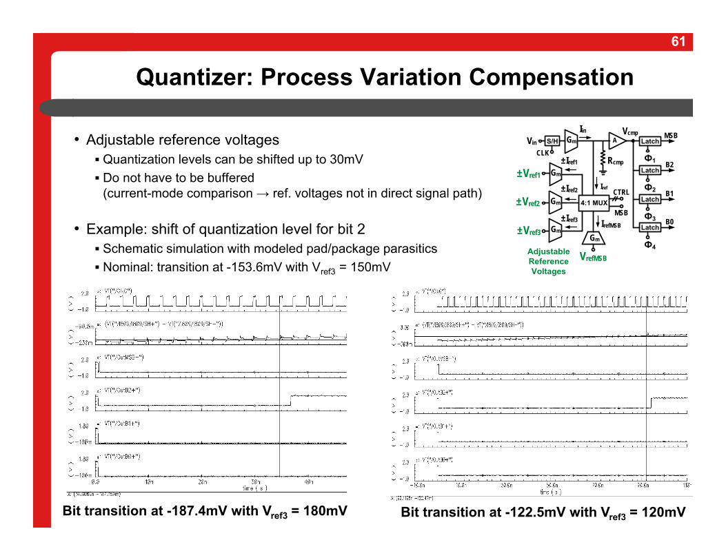
Quantizer: Process Variation Compensation
• Adjustable reference voltages Quantization levels can be shifted up to 30mV Do not have to be buffered
(current-mode comparison → ref. voltages not in direct signal path)
• Example: shift of quantization level for bit 2 Schematic simulation with modeled pad/package parasitics Nominal: transition at -153.6mV with Vref3 = 150mV
Bit transition at -187.4mV with Vref3 = 180mV Bit transition at -122.5mV with Vref3 = 120mV
Vin S/H
CLK
±Vref1
±Vref2
±Vref3
Iin
±Iref1
±Iref2
±Iref3
4:1 MUXMSB
Iref CTRL
Rcmp
A LatchMSB
Ф1Latch
B2
Ф2Latch
B1
Ф3Latch
B0
Ф4
Gm
Gm
Gm
GmGm
VrefMSB
Vcmp
IrefMSB
Adjustable Reference Voltages
62
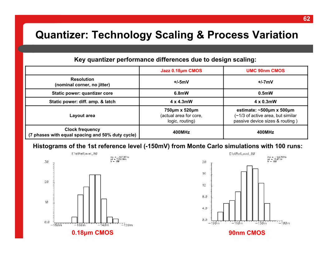
Quantizer: Technology Scaling & Process Variation
0.18μm CMOS 90nm CMOS
Jazz 0.18μm CMOS UMC 90nm CMOS
Resolution(nominal corner, no jitter) +/-5mV +/-7mV
Static power: quantizer core 6.8mW 0.5mW
Static power: diff. amp. & latch 4 x 4.3mW 4 x 0.3mW
Layout area750μm x 520μm
(actual area for core, logic, routing)
estimate: ~500μm x 500μm(~1/3 of active area, but similar passive device sizes & routing )
Clock frequency(7 phases with equal spacing and 50% duty cycle) 400MHz 400MHz
Key quantizer performance differences due to design scaling:
Histograms of the 1st reference level (-150mV) from Monte Carlo simulations with 100 runs:
63
Quantizer: Summary & Conclusions
• Functionality verified through measurementsQuantizer operated within a Σ∆ ADC prototype (0.18μm CMOS technology)
• Quantization with multi-phase clocks provides a viable alternative to typical flash quantizers in Σ∆ modulators Optimized for combination with a single-element PWM DAC that avoids unit element
mismatch problems due to process variationsBenefits from fast-switching transistors in modern CMOS technologiesFor the same specifications: power of 90nm design < 10% power of 0.18μm design
• Tuning “knobs” are available to compensate for PVT variationsQuantization levels can be shifted individually via reference voltage adjustments
• A low-jitter clock source is mandatory< 50ps RMS period jitter is required for the standalone 3-bit quantizer operation
C.-Y. Lu, M. Onabajo, V. Gadde, Y.-C. Lo, H.-P. Chen, V. Periasamy, and J. Silva-Martinez, “A 25MHz bandwidth 5th-order continuous-time lowpass sigma-delta modulator with 67.7dB SNDR using time-domain quantization andfeedback,” IEEE J. Solid-State Circuits, vol. 45, no. 9, pp. 1795-1808, Sept. 2010.

Thank You.


![Adaptive CMOS Circuits for 4G Wireless Networksdigital.csic.es/bitstream/10261/3754/1/ECCTD07_TutorialJrosa.pdf · Adaptive CMOS Circuits for 4G Wireless Networks ... [UMTS/WCDMA]](https://static.fdocument.org/doc/165x107/5ae0f6c27f8b9af05b8e5633/adaptive-cmos-circuits-for-4g-wireless-cmos-circuits-for-4g-wireless-networks-.jpg)