Lecture 2 Chapter 2 MOS Transistors. Voltage along the channel V(y) = the voltage at a distance y...
36
Lecture 2 Chapter 2 MOS Transistors
-
Upload
jacob-wood -
Category
Documents
-
view
213 -
download
0
Transcript of Lecture 2 Chapter 2 MOS Transistors. Voltage along the channel V(y) = the voltage at a distance y...

Lecture 2
Chapter 2 MOS Transistors

Voltage along the channel
V(y) = the voltage at a distance y along the channelV(y) is constrained by the following relationship: 0<V(y)<VDS

Inversion Layer Charge
In order to have any inversion layer charge, VGC > VT.
Q=CV →Qn(y)=Cox(VGS-V(y)-VT)[Cox]=fF/μm2
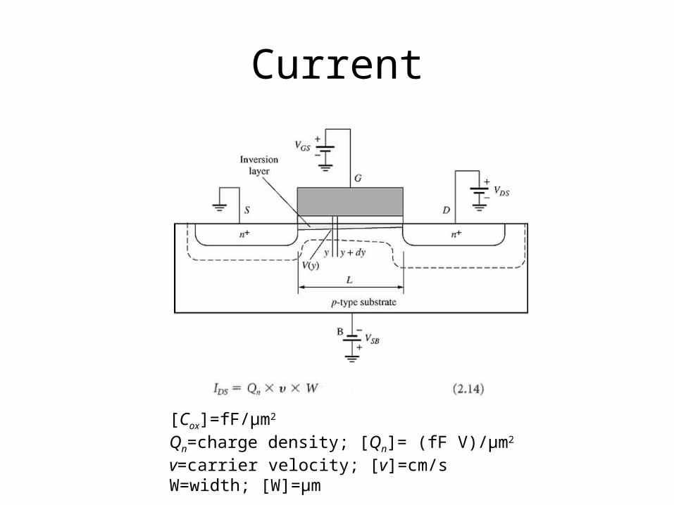
Current
[Cox]=fF/μm2
Qn=charge density; [Qn]= (fF V)/μm2
v=carrier velocity; [v]=cm/sW=width; [W]=μm

Carrier Velocity
v=carrier velocity; [v]=cm/secμ=mobility; [μ]=cm2/(V-sec)E=electric field; [E]=V/cm
Generic relationship between μ, v, and E
𝑣=𝜇𝐸
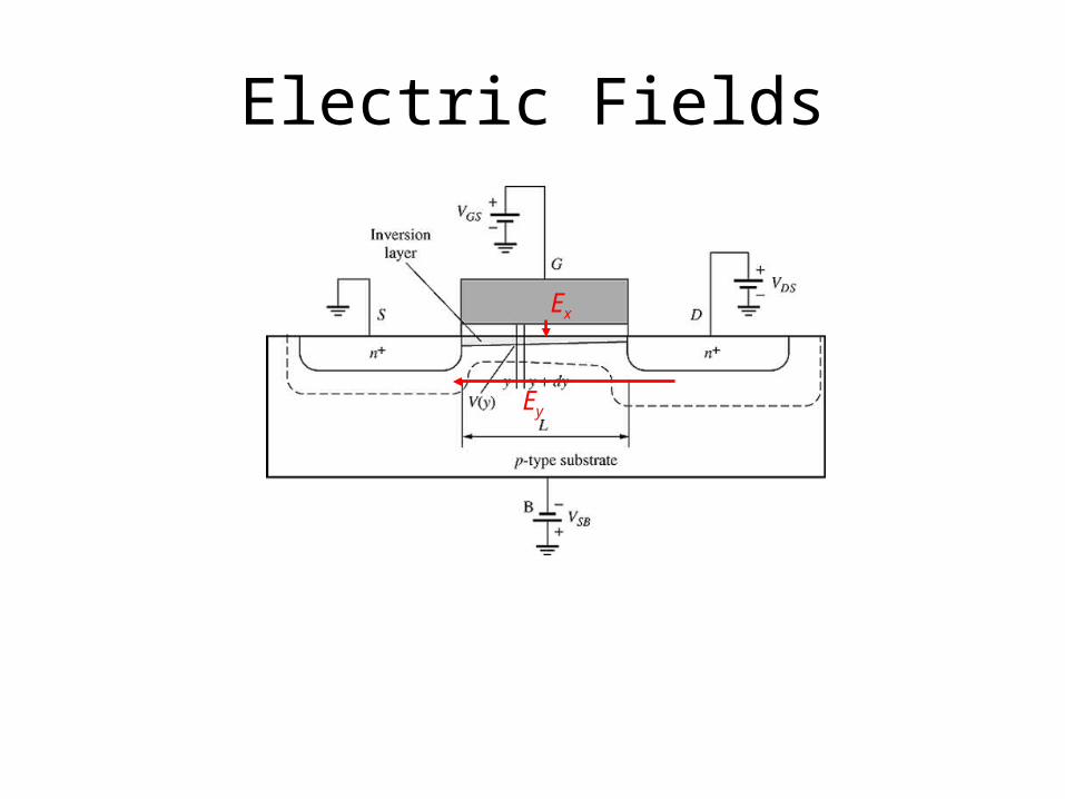
Electric Fields
Ex
Ey

Vertical Electrical Field (Ex)
• Ex is approximately VDD/tox

Reduced Mobility Due to Ex
• For high gate voltages, the mobility of carriers decreases due to electron caused by dangling bond at the Si-SiO2 interface
• Mathematically, the reduced mobility due to Ex can be modeled as
μe: effect of Ex on the nominal mobilityμo: the nominal mobility

Horizontal Electric Field (Ey)
• Ey is approximately VDS/L
• Ey acts to – push the carriers to their velocity limit– Reduce carrier mobility

Carrier Velocity Vs. Ey
The slope of v versus Ey is μ, the mobility.
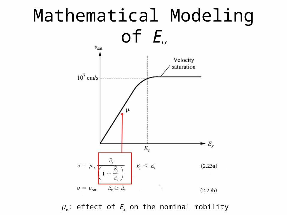
Mathematical Modeling of Ey
μe: effect of Ex on the nominal mobility

Transistor in the Linear Region
• Assume that Ey<EC
• Therefore,

Transistor in the Linear Region
Left Side: 0 to LRight Side: 0 to VDS
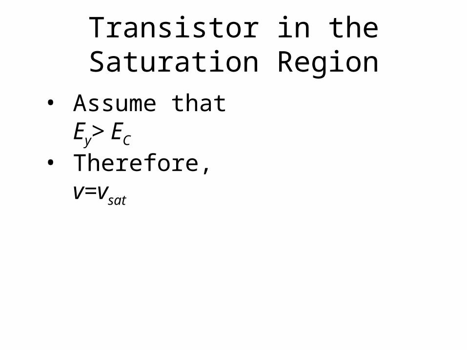
Transistor in the Saturation Region
• Assume that Ey> EC
• Therefore, v=vsat

Determine VDSAT
• Assumption: the current is the same throughout the channel→V(y)=VDS
• Solve for VDSAT by applying the boundary condition: IDS(triode)=IDS(sat)
• VDSAT=(VGS-VT)||LEC (See notes)

MOS Transistor in Saturation
Substitute VDSAT for VDS in EQ 2.27. (See Notes for details)
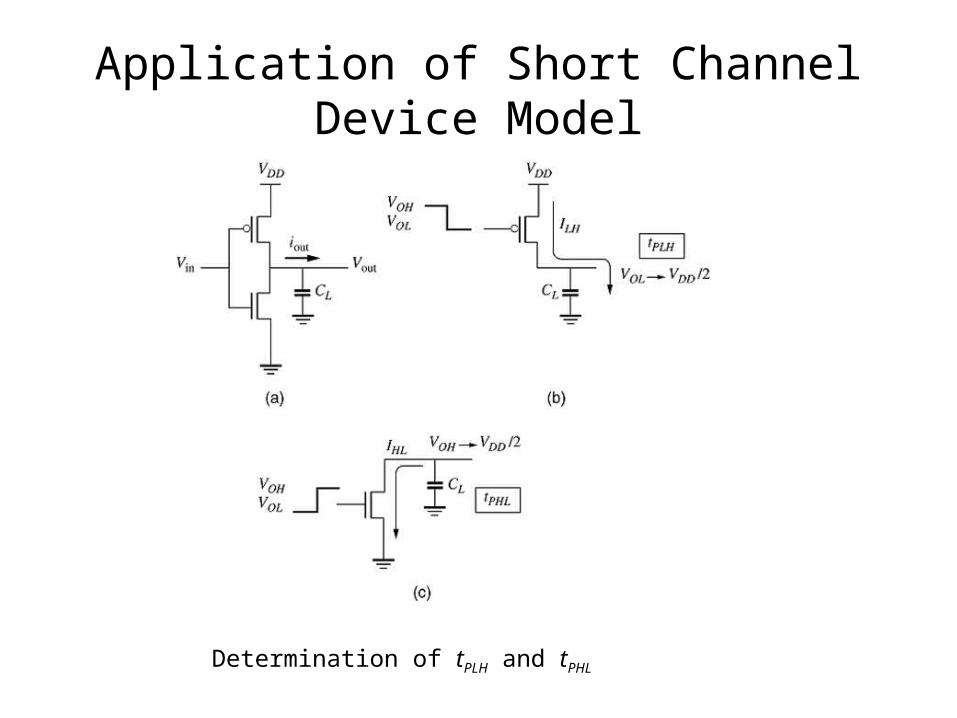
Application of Short Channel Device Model
Determination of tPLH and tPHL

Inverter Delay Calculation
• Example 6.1 • tp=propagation delay
• tp=CL (VDD)/(2IDSAT)=0.7REQ(L/W)CL
– REQ=(VDD/2)/(0.7 IDSAT)

Significance of Leakage Power
An increase in static power dissipation

Leakage Current
• Sources–Subthreshold conduction–Gate leakage–Junction leakage

Subthreshold Current• The long-channel transistor I-V model assumes
current only flows when VGS>VT
• In real transistors, current does not abruptly cut off below the threshold.
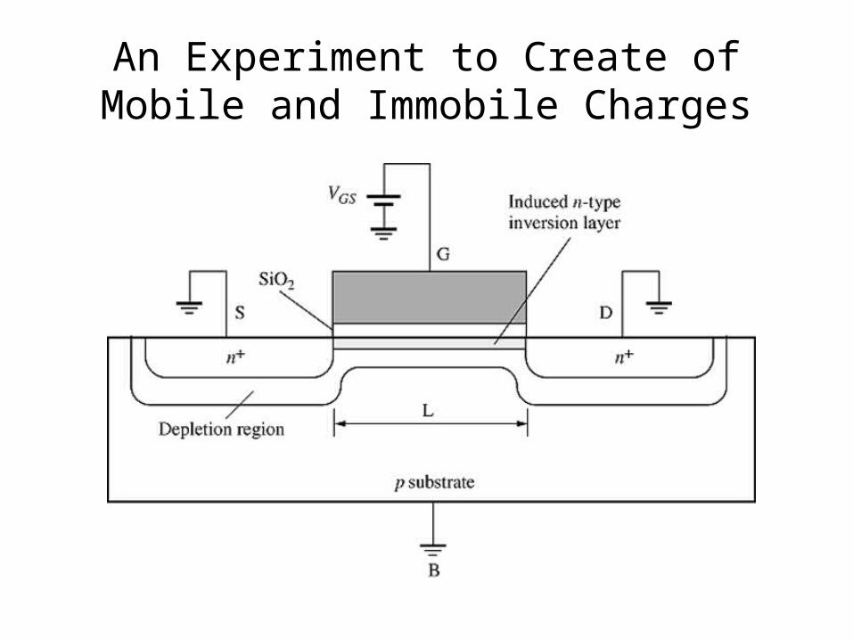
An Experiment to Create of Mobile and Immobile Charges
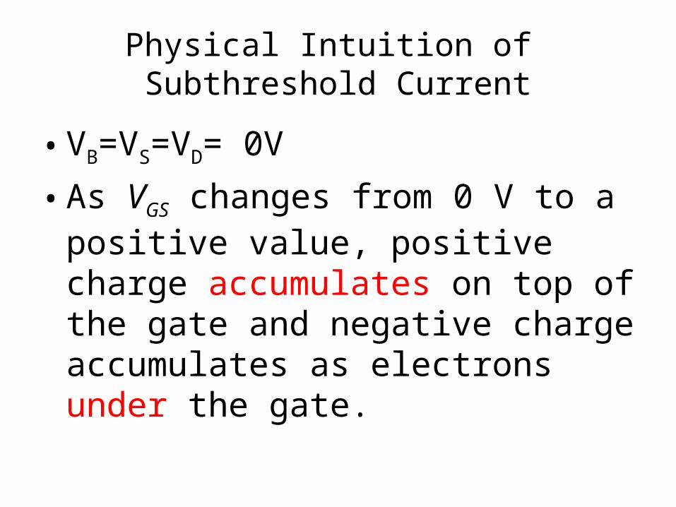
Physical Intuition of Subthreshold Current
• VB=VS=VD= 0V
• As VGS changes from 0 V to a positive value, positive charge accumulates on top of the gate and negative charge accumulates as electrons under the gate.

Immobile Charges Under the gate
• Initially, the negative charge in the p-type body is manifested by creation of a depletion region in which mobile holes are pushed under the gate, leaving behind negatively charged immobile (fixed) acceptor ions.

Mobile Charges Under the Gate
• As the gate voltage continues to increase, the depletion layer thickness increases and eventually an initial layer of mobile electrons appears at the surface of the silicon in the so-called weak inversion condition.
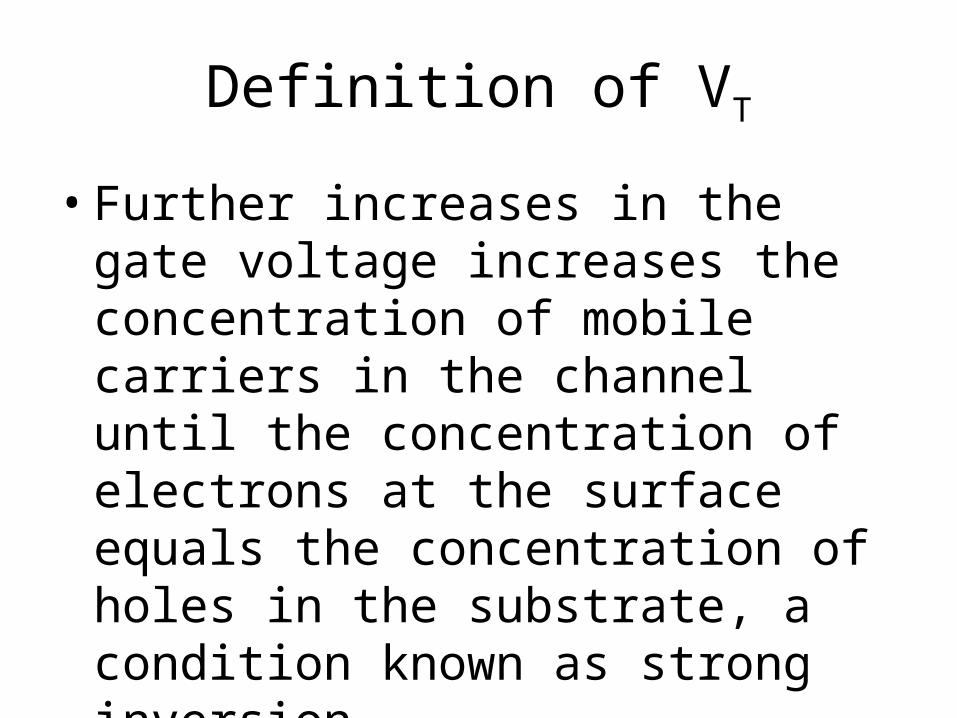
Definition of VT
• Further increases in the gate voltage increases the concentration of mobile carriers in the channel until the concentration of electrons at the surface equals the concentration of holes in the substrate, a condition known as strong inversion

Linear Increase in Mobile charge for VGS>VT
• For gate voltage above this point, the depletion layer thickness remains constant while the additional charge on the gate is matched by the additional mobile carriers in the channel drawn from source and drain.

Fixed Charge Vs. Mobile Charge

Mobile Charge on a Log Scale

Similarity to BJT• An NPN• Mobile minority carrier in the P region• Contrast: The base potential is controlled
through a capacitive divder.

Subthreshold Current Equation
• Vt0, the threshold voltage• Sensitivity to Vds
• vT is kT/q
[Source: Weste]

Reduce Isub via Vt0• Vt0 controls the magnitude of the
subthreshold current• Trade off–Keep Vt0 to lower subthreshold current–Price: VDD-Vt0 ↔Speed suffers
• Increase the substrate bias as a means to increase Vt0, and thus reduce subthreshold current for inactive circuits –Difficult to implement for high speed
circuits
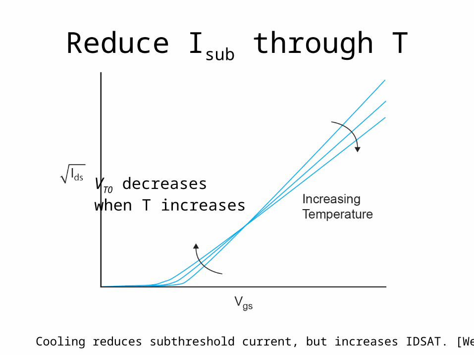
Reduce Isub through T
VT0 decreases when T increases
Cooling reduces subthreshold current, but increases IDSAT. [Weste]

Application
• Thse subthreshold conduction is used to advantage in low power circuits
• The subthreshold current adversely dynamic circuits and DRAMs, which depend on the storage of charge on a capacitor

Gate Leakage
Gate leaking is due to tunneling of charges through the oxide.Cox helps attract charge to the channel.By using hi K dielectric, thicker tox can be used to reduce gate leakge.

Leakage due to reverse diode current
Usually negligible for digital applications