LB Q39G - TME
22
LB Q39G 1 Version 1.5 | 2018-03-27 www.osram-os.com LB Q39G CHIPLED ® 0603 Applications — Electronic Equipment — Gaming, Amusement, Gambling — White Goods Features: — Package: SMT package 0603, colorless diffused resin — Chip technology: InGaN on Sapphire — Typ. Radiation: 170° (horizontal), 130° (vertical) — Color: λ dom = 470 nm ( ● blue) — Corrosion Robustness Class: 3B — ESD: 2 kV acc. to ANSI/ESDA/JEDEC JS-001 (HBM)
Transcript of LB Q39G - TME
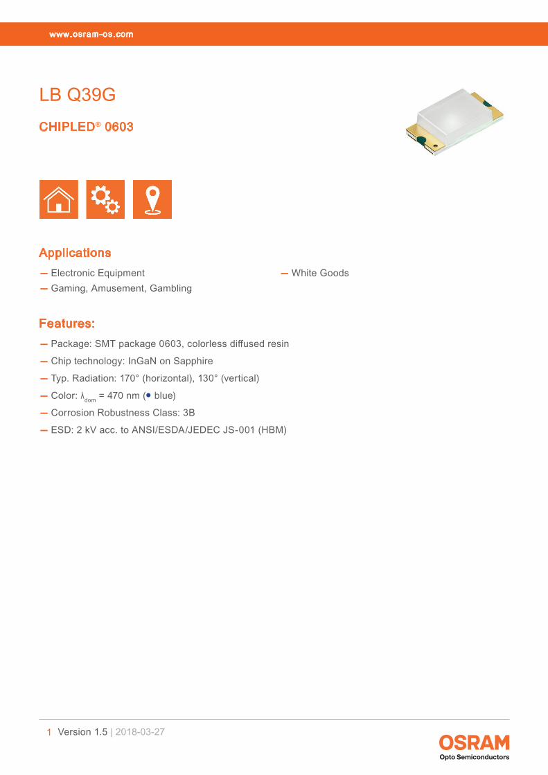
LB Q39G
1 Version 1.5 | 2018-03-27
Produktdatenblatt | Version 1.1 www.osram-os.com
LB Q39G
CHIPLED® 0603
Applications — Electronic Equipment — Gaming, Amusement, Gambling
— White Goods
Features: — Package: SMT package 0603, colorless diffused resin
— Chip technology: InGaN on Sapphire
— Typ. Radiation: 170° (horizontal), 130° (vertical)
— Color: λdom = 470 nm (● blue)
— Corrosion Robustness Class: 3B
— ESD: 2 kV acc. to ANSI/ESDA/JEDEC JS-001 (HBM)

LB Q39G
2 Version 1.5 | 2018-03-27
Ordering Information
Type Luminous Intensity 1) Ordering CodeIF = 5 mAIv
LB Q39G-N1OO-35-1 ≥ 28.0 mcd Q65110A7940

LB Q39G
3 Version 1.5 | 2018-03-27
Maximum RatingsParameter Symbol Values
Operating Temperature Top min. max.
-30 °C 85 °C
Storage Temperature Tstg min. max.
-40 °C 85 °C
Junction Temperature Tj max. 95 °C
Forward current TA = 25 °C
IF max. 15 mA
Surge Current t ≤ 10 µs; D = 0.005 ; TA = 25 °C
IFS max. 100 mA
Reverse voltage 2) TA = 25 °C
VR max. 5 V
ESD withstand voltage acc. to ANSI/ESDA/JEDEC JS-001 (HBM)
VESD 2 kV

LB Q39G
4 Version 1.5 | 2018-03-27
CharacteristicsIF = 5 mA; TA = 25 °C
Parameter Symbol Values
Peak Wavelength 3) λpeak typ. 465 nm
Dominant Wavelength 3) λdom min. typ. max.
464 nm 470 nm 476 nm
Spectral Bandwidth at 50% Irel,max ∆λ typ. 22 nm
Viewing angle at 50 % IV values for 0°, 90°
2φ typ. typ.
170 ° 130 °
Forward Voltage 4) IF = 5 mA
VF min. typ. max.
2.60 V 2.85 V 3.10 V
Reverse current 2) VR = 5 V
IR typ. max.
0.01 µA 10 µA
Real thermal resistance junction/ambient 5), 6) RthJA real max. 650 K / W
Real thermal resistance junction/solderpoint 5) RthJS real max. 370 K / W
LB Q39G
5 Version 1.5 | 2018-03-27
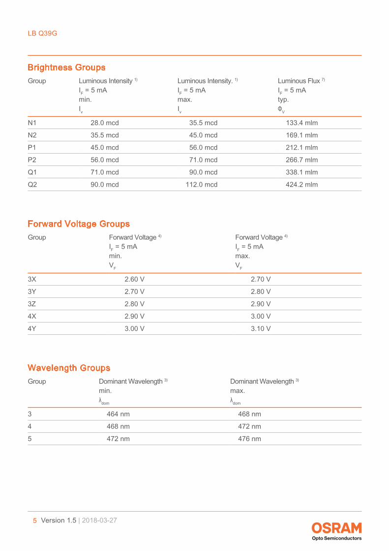
Brightness Groups
Group Luminous Intensity 1) Luminous Intensity. 1) Luminous Flux 7)
IF = 5 mA IF = 5 mA IF = 5 mAmin. max. typ.Iv Iv ΦV
N1 28.0 mcd 35.5 mcd 133.4 mlm
N2 35.5 mcd 45.0 mcd 169.1 mlm
P1 45.0 mcd 56.0 mcd 212.1 mlm
P2 56.0 mcd 71.0 mcd 266.7 mlm
Q1 71.0 mcd 90.0 mcd 338.1 mlm
Q2 90.0 mcd 112.0 mcd 424.2 mlm
Forward Voltage Groups
Group Forward Voltage 4) Forward Voltage 4)
IF = 5 mA IF = 5 mAmin. max.VF VF
3X 2.60 V 2.70 V
3Y 2.70 V 2.80 V
3Z 2.80 V 2.90 V
4X 2.90 V 3.00 V
4Y 3.00 V 3.10 V
Wavelength Groups
Group Dominant Wavelength 3) Dominant Wavelength 3)
min. max.λdom λdom
3 464 nm 468 nm
4 468 nm 472 nm
5 472 nm 476 nm

LB Q39G
6 Version 1.5 | 2018-03-27
Group Name on Label Example: N1-3-3XBrightness Wavelength Forward Voltage
N1 3 3X
LB Q39G
7 Version 1.5 | 2018-03-27
LB Q39G
350 400 450 500 550 600 650 700 750 800
λ [nm]
0,0
0,2
0,4
0,6
0,8
1,0Irel
: blue: Vλ
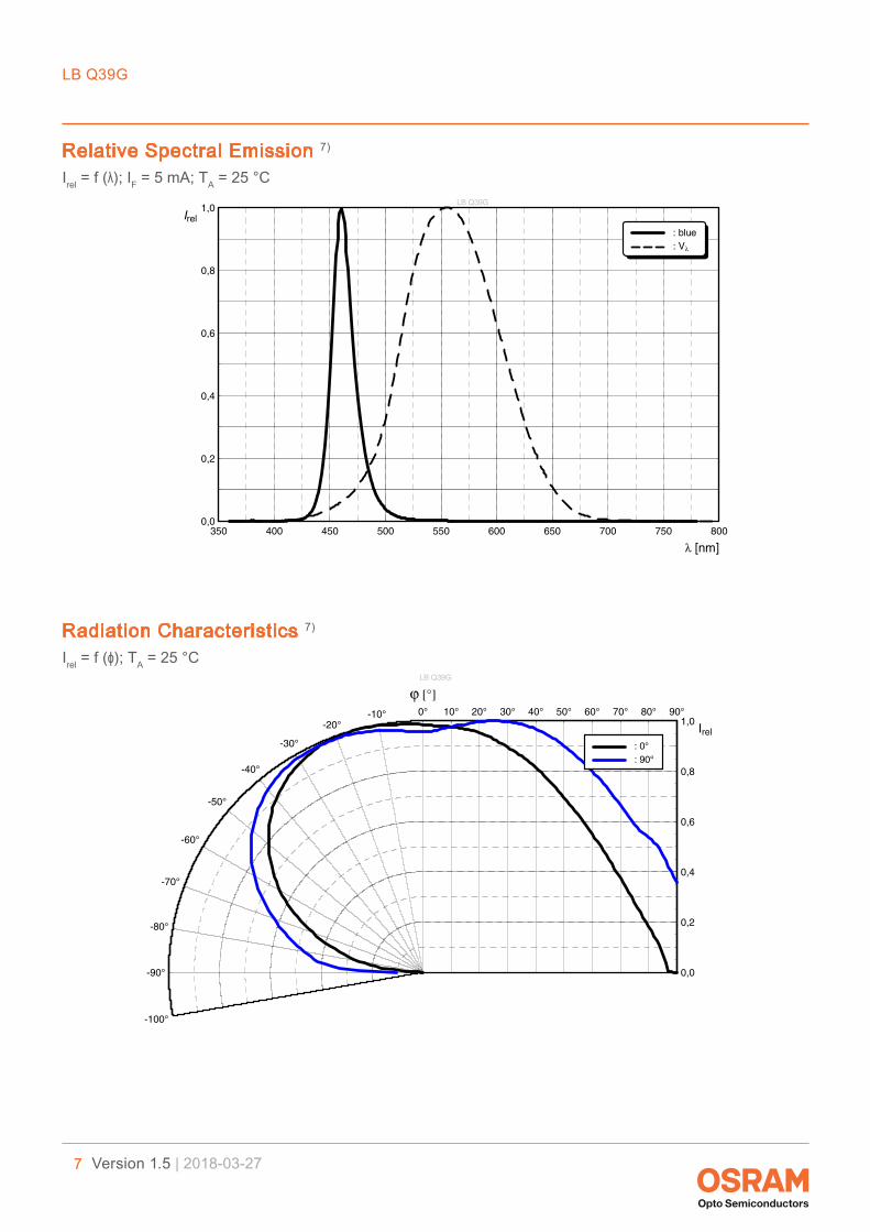
Relative Spectral Emission 7) Irel = f (λ); IF = 5 mA; TA = 25 °C
LB Q39G
-100°
-90°
-80°
-70°
-60°
-50°
-40°
-30°
-20°-10° 0° 10° 20° 30° 40° 50° 60° 70° 80° 90°
ϕ [°]
0,0
0,2
0,4
0,6
0,8
1,0Irel
: 0°: 90°
Radiation Characteristics 7) Irel = f (ϕ); TA = 25 °C
LB Q39G
8 Version 1.5 | 2018-03-27
LB Q39G
0,91 2 3 4 5 6 7 8 9 10
IF [mA]
0,3
0,4
0,5
0,6
0,7
0,80,9
1
2
3IV
IV(5mA)
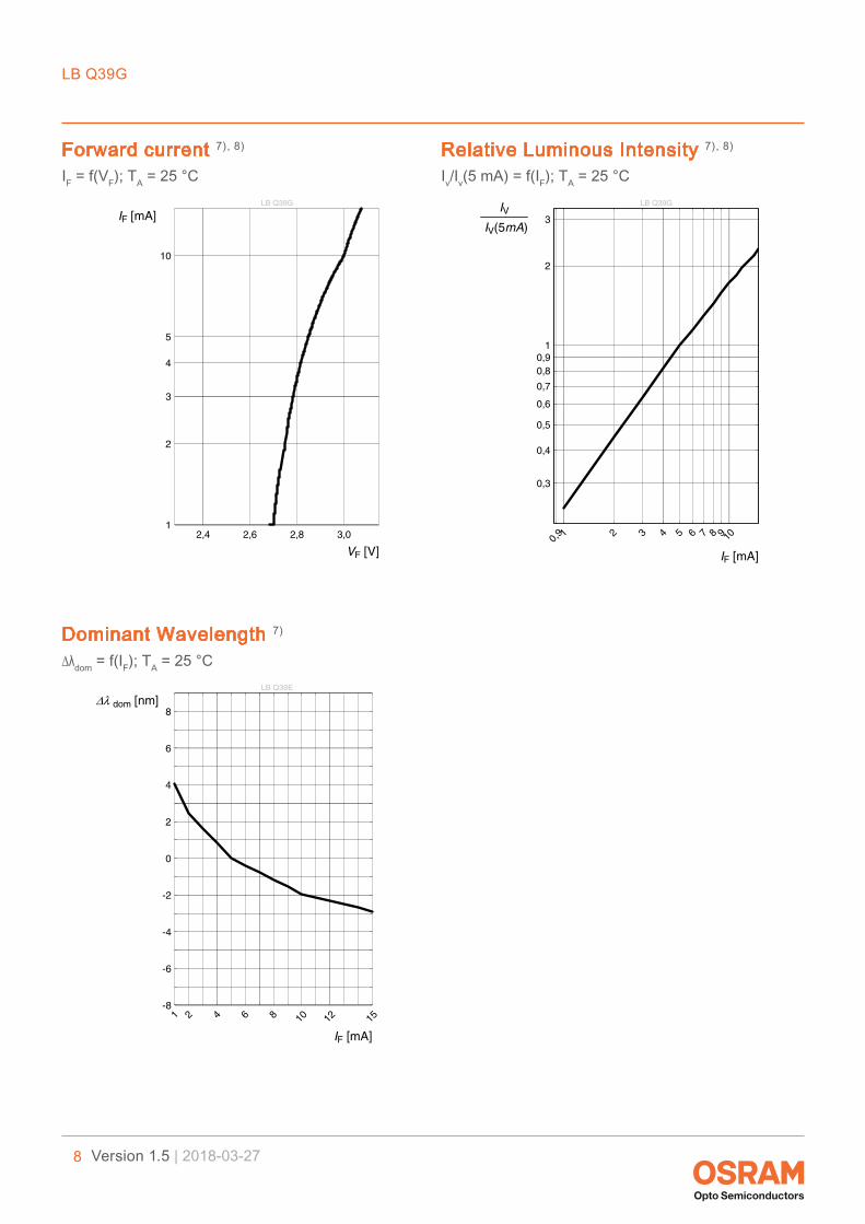
Relative Luminous Intensity 7), 8)
Iv/Iv(5 mA) = f(IF); TA = 25 °C
LB Q39G
2,4 2,6 2,8 3,0
VF [V]
1
2
3
4
5
10
IF [mA]
Forward current 7), 8)
IF = f(VF); TA = 25 °C
LB Q39E
1 152 4 6 8 10 12
IF [mA]
-8
-6
-4
-2
0
2
4
6
8∆λ dom [nm]
Dominant Wavelength 7)
∆λdom = f(IF); TA = 25 °C

LB Q39G
9 Version 1.5 | 2018-03-27
LB Q39G
30 40 50 60 70 80
Tj [°C]
0,0
0,2
0,4
0,6
0,8
1,0
1,2IvIv(25°C)
Relative Luminous Intensity 7)
Iv/Iv(25 °C) = f(Tj); IF = 5 mA
LB Q39G
30 40 50 60 70 80
Tj [°C]
-0,16
-0,14
-0,12
-0,10
-0,08
-0,06
-0,04
-0,02
0,00∆VF [V]
Forward Voltage 7)
∆VF = VF - VF(25 °C) = f(Tj); IF = 5 mA
LB Q39G
30 40 50 60 70 80
Tj [°C]
-10
-5
0
5
10∆λ dom [nm]
Dominant Wavelength 7)
∆λdom = λdom - λdom(25 °C) = f(Tj); IF = 5 mA
LB Q39G
10 Version 1.5 | 2018-03-27
00
˚CT
IFmA
OHL03587
TSTA
temp. ambientTtemp. solder pointST
A
20 40 60 80 100
2
4
6
8
10
12
14
16
20
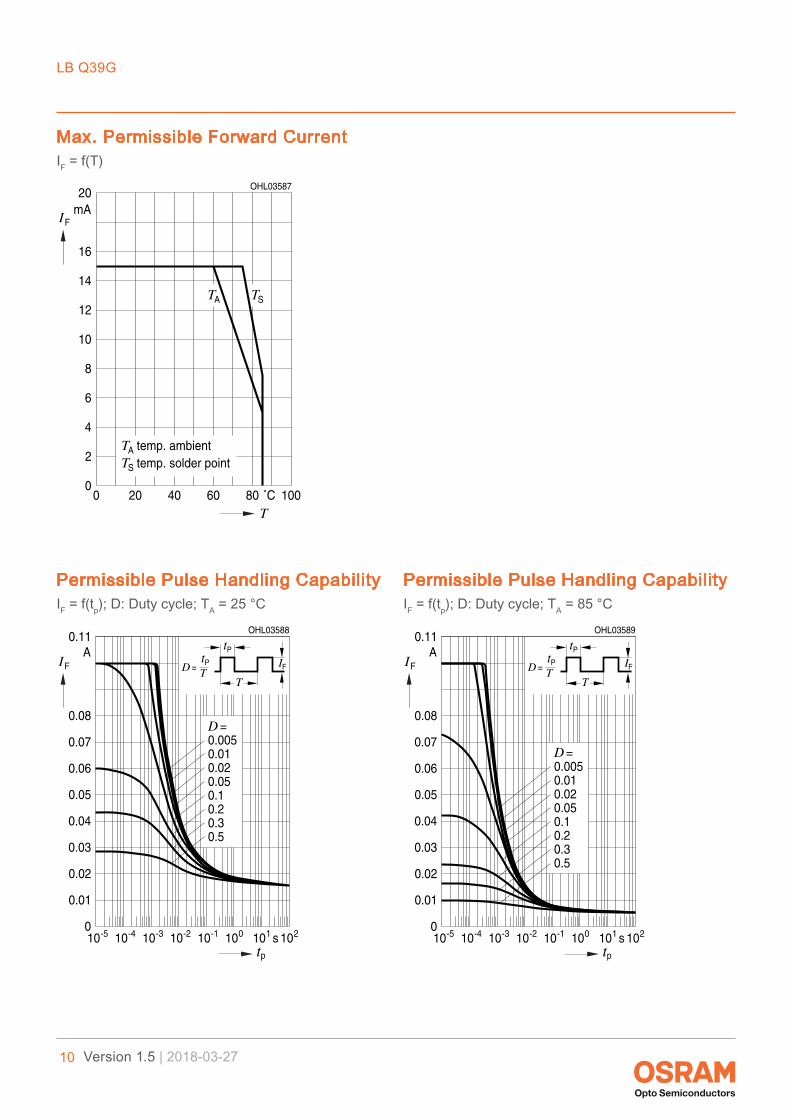
Max. Permissible Forward CurrentIF = f(T)
0-5
FIA
tp
s
OHL03589
-410 -310 -210 -110 010 110 21010
0.01
0.1
0.020.05
0.005D =
T
tTD = P
PtIF
0.20.30.5
0.01
0.02
0.03
0.04
0.05
0.06
0.07
0.08
0.11
Permissible Pulse Handling CapabilityIF = f(tp); D: Duty cycle; TA = 85 °C
0-5
FIA
tp
s
OHL03588
-410 -310 -210 -110 010 110 21010
0.01
0.1
0.020.05
0.005D =
T
tTD = P
PtIF
0.20.30.5
0.01
0.02
0.03
0.04
0.05
0.06
0.07
0.08
0.11
Permissible Pulse Handling CapabilityIF = f(tp); D: Duty cycle; TA = 25 °C
LB Q39G
11 Version 1.5 | 2018-03-27
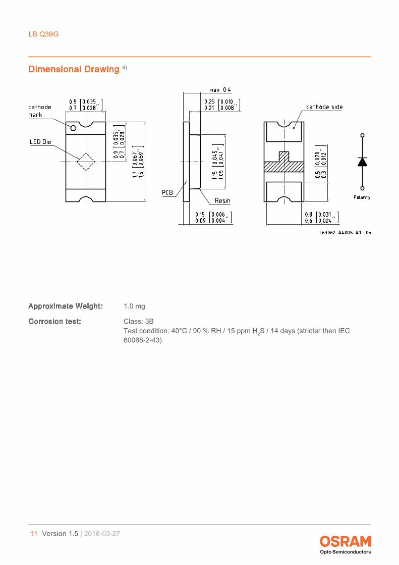
Dimensional Drawing 9)
Approximate Weight: 1.0 mg
Corrosion test: Class: 3B Test condition: 40°C / 90 % RH / 15 ppm H2S / 14 days (stricter then IEC 60068-2-43)
LB Q39G
12 Version 1.5 | 2018-03-27
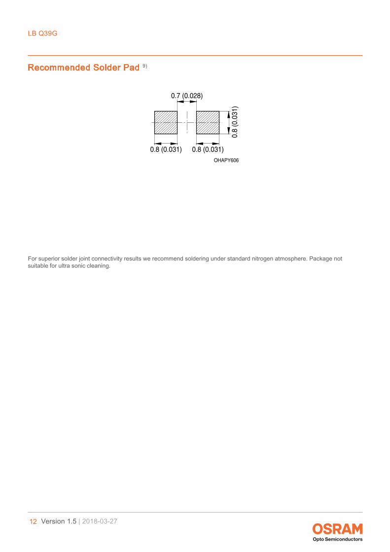
For superior solder joint connectivity results we recommend soldering under standard nitrogen atmosphere. Package not suitable for ultra sonic cleaning.
Recommended Solder Pad 9)
0.8 (0.031)
0.7 (0.028)
OHAPY606
0.8
(0.0
31)
0.8 (0.031)
LB Q39G
13 Version 1.5 | 2018-03-27
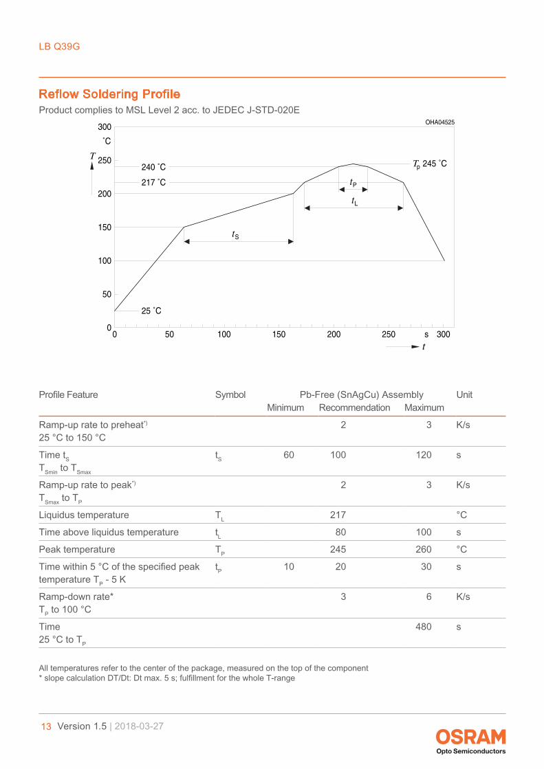
Reflow Soldering ProfileProduct complies to MSL Level 2 acc. to JEDEC J-STD-020E
00
s
OHA04525
50
100
150
200
250
300
50 100 150 200 250 300t
T
˚C
St
t
Pt
Tp240 ˚C
217 ˚C
245 ˚C
25 ˚C
L
Profile Feature Symbol Pb-Free (SnAgCu) Assembly UnitMinimum Recommendation Maximum
Ramp-up rate to preheat*)
25 °C to 150 °C2 3 K/s
Time tSTSmin to TSmax
tS 60 100 120 s
Ramp-up rate to peak*)
TSmax to TP
2 3 K/s
Liquidus temperature TL 217 °C
Time above liquidus temperature tL 80 100 s
Peak temperature TP 245 260 °C
Time within 5 °C of the specified peaktemperature TP - 5 K
tP 10 20 30 s
Ramp-down rate*TP to 100 °C
3 6 K/s
Time25 °C to TP
480 s
All temperatures refer to the center of the package, measured on the top of the component* slope calculation DT/Dt: Dt max. 5 s; fulfillment for the whole T-range
LB Q39G
14 Version 1.5 | 2018-03-27
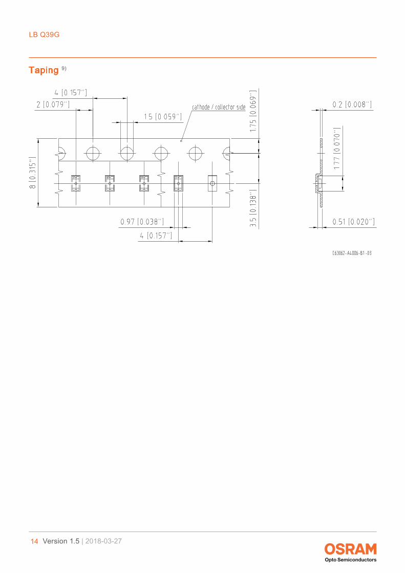
Taping 9)
LB Q39G
15 Version 1.5 | 2018-03-27
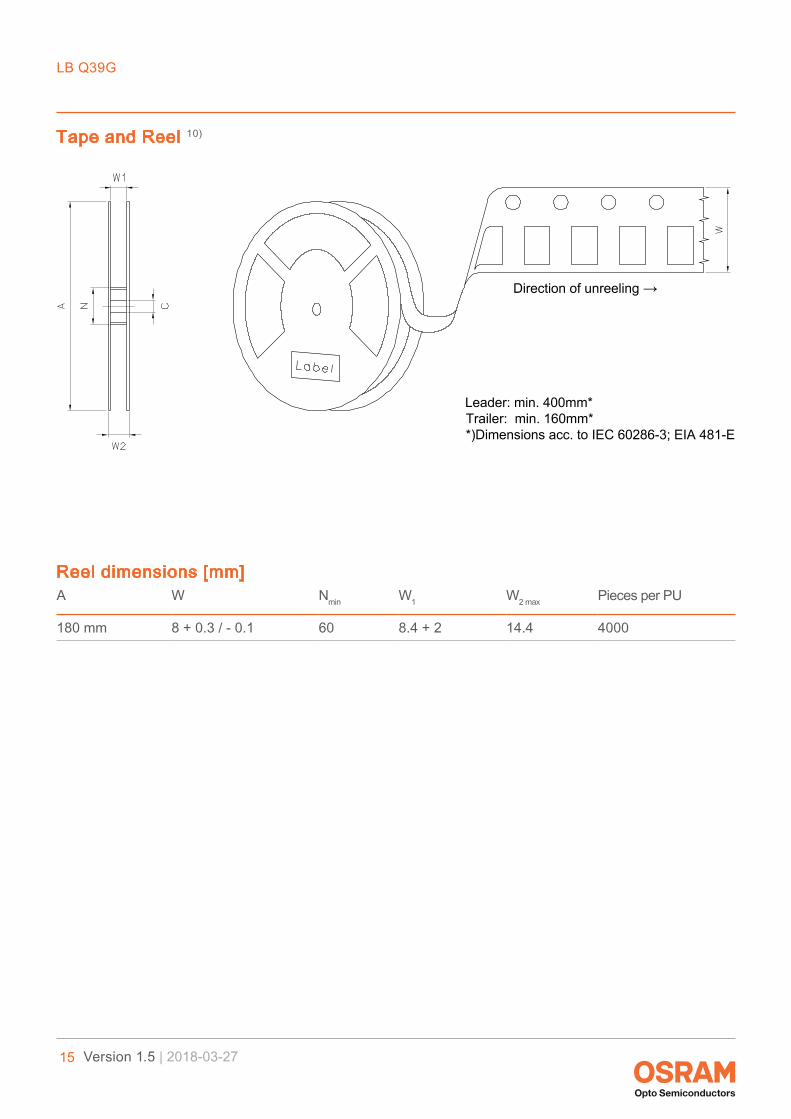
Tape and Reel 10)
Reel dimensions [mm]A W Nmin W1 W2 max Pieces per PU
180 mm 8 + 0.3 / - 0.1 60 8.4 + 2 14.4 4000
LB Q39G
16 Version 1.5 | 2018-03-27
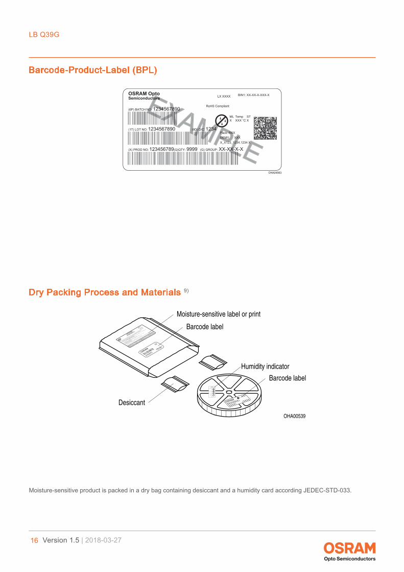
Barcode-Product-Label (BPL)
Moisture-sensitive product is packed in a dry bag containing desiccant and a humidity card according JEDEC-STD-033.
Dry Packing Process and Materials 9)
OHA00539
OSRAM
Moisture-sensitive label or print
Barcode label
Desiccant
Humidity indicator
Barcode label
OSRAM
Please check the HIC immidiately afterbag opening.
Discard if circles overrun.Avoid metal contact.
WET
Do not eat.
Comparatorcheck dot
parts still adequately dry.
examine units, if necessary
examine units, if necessary
5%
15%
10%bake units
bake units
If wet,
change desiccant
If wet,
Humidity IndicatorMIL-I-8835
If wet,
Mois
ture
Level 3
Flo
or tim
e 168 H
ours
Mois
ture
Level 6
Flo
or tim
e 6
Hours
a) H
umid
ity In
dicato
r C
ard is
> 1
0% w
hen read a
t 23 ˚
C ±
5 ˚C
, or
reflo
w, v
apor-phase r
eflow
, or equiv
alent p
rocessin
g (peak p
ackage
2. Afte
r th
is b
ag is o
pened, devic
es that w
ill b
e subje
cted to
infrare
d
1. Shelf
life in
seale
d bag: 2
4 month
s at <
40 ˚
C a
nd < 9
0% rela
tive h
umid
ity (R
H).
Mois
ture
Level 5
a
at facto
ry c
onditions o
f
(if b
lank, s
eal date
is id
entical w
ith d
ate c
ode).
a) M
ounted w
ithin
b) S
tore
d at
body tem
p.
3. Devic
es require
bakin
g, befo
re m
ounting, i
f:
Bag s
eal date
Mois
ture
Level 1
Mois
ture
Level 2
Mois
ture
Level 2
a4. If b
aking is
require
d,
b) 2a o
r 2b is
not m
et.
Date
and ti
me o
pened:
refe
rence IP
C/J
ED
EC
J-S
TD
-033 fo
r bake p
rocedure
.
Flo
or tim
e see b
elow
If bla
nk, see b
ar code la
bel
Flo
or tim
e > 1
Year
Flo
or tim
e 1
Year
Flo
or tim
e 4
Weeks10%
RH
.
_<
Mois
ture
Level 4
Mois
ture
Level 5
˚C).
OPTO
SEM
ICO
NDUCTORS
MO
ISTURE S
ENSITIV
E
This b
ag conta
ins
CAUTION
Flo
or tim
e 72 H
ours
Flo
or tim
e 48 H
ours
Flo
or tim
e 24 H
ours
30 ˚C
/60%
RH
.
_<
LE
VE
L
If bla
nk, see
bar code la
bel
LB Q39G
17 Version 1.5 | 2018-03-27
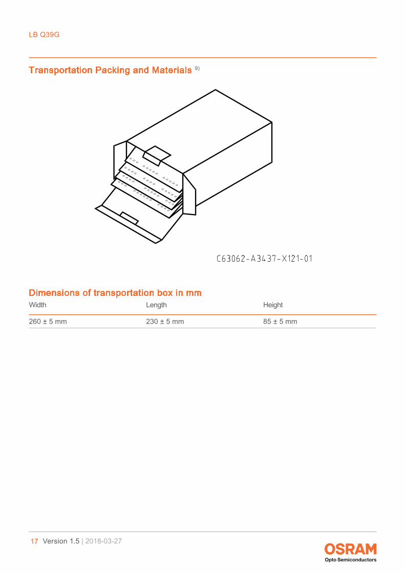
Transportation Packing and Materials 9)
Dimensions of transportation box in mmWidth Length Height
260 ± 5 mm 230 ± 5 mm 85 ± 5 mm
LB Q39G
18 Version 1.5 | 2018-03-27
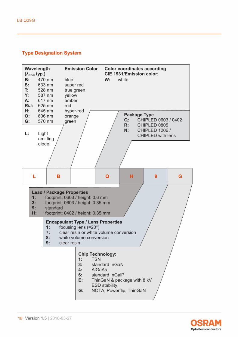
Chip Technology: 1: TSN 3: standard InGaN 4: AlGaAs 6: standard InGalP E: ThinGaN & package with 8 kV ESD stability G: NOTA, Powerflip, ThinGaN
´ Encapsulant Type / Lens Properties 1: focusing lens (=20°) 7: clear resin or white volume conversion 8: white volume conversion 9: clear resin
Wavelength Emission Color Color coordinates according (λdom typ.) CIE 1931/Emission color: B: 470 nm blue W: white S: 633 nm super red T: 528 nm true green Y: 587 nm yellow A: 617 nm amber R/J: 625 nm red H: 645 nm hyper-red O: 606 nm orange G: 570 nm green
L: Light emitting diode
Package Type Q: CHIPLED 0603 / 0402 R: CHIPLED 0805 N: CHIPLED 1206 /
CHIPLED with lens
Lead / Package Properties 1: footprint: 0603 / height: 0.6 mm 3: footprint: 0603 / height: 0.35 mm 9: standard H: footprint: 0402 / height: 0.35 mm
Type Designation System
L B Q H 9 G
LB Q39G
19 Version 1.5 | 2018-03-27
NotesThe evaluation of eye safety occurs according to the standard IEC 62471:2006 (photo biological safety of lamps and lamp systems). Within the risk grouping system of this IEC standard, the LED specified in this data sheet fall into the class exempt group (exposure time 10000 s). Under real circumstances (for expo-sure time, eye pupils, observation distance), it is assumed that no endangerment to the eye exists from these devices. As a matter of principle, however, it should be mentioned that intense light sources have a high secondary exposure potential due to their blinding effect. As is also true when viewing other bright light sources (e.g. headlights), temporary reduction in visual acuity and afterimages can occur, leading to irrita-tion, annoyance, visual impairment, and even accidents, depending on the situation.
Subcomponents of this LED contain, in addition to other substances, metal filled materials including silver. Metal filled materials can be affected by environments that contain traces of aggressive substances. There-fore, we recommend that customers minimize LED exposure to aggressive substances during storage, pro-duction, and use. LEDs that showed visible discoloration when tested using the described tests above did show no performance deviations within failure limits during the stated test duration. Respective failure limits are described in the IEC60810.
Based on very short life cycle times in chip technology this component is subject to frequent adaption to the latest chip technology.
For further application related informations please visit www.osram-os.com/appnotes
LB Q39G
20 Version 1.5 | 2018-03-27
Disclaimer
DisclaimerLanguage english will prevail in case of any discrepancies or deviations between the two language word-ings.
Attention please!The information describes the type of component and shall not be considered as assured characteristics. Terms of delivery and rights to change design reserved. Due to technical requirements components may contain dangerous substances.For information on the types in question please contact our Sales Organization.If printed or downloaded, please find the latest version on the OSRAM OS webside.
PackingPlease use the recycling operators known to you. We can also help you – get in touch with your nearest sales office.By agreement we will take packing material back, if it is sorted. You must bear the costs of transport. For packing material that is returned to us unsorted or which we are not obliged to accept, we shall have to invoice you for any costs incurred.
Product safety devices/applications or medical devices/applicationsOSRAM OS components are not developed, constructed or tested for the application as safety relevant component or for the application in medical devices.
In case Buyer – or Customer supplied by Buyer– considers using OSRAM OS components in product safety devices/applications or medical devices/applications, Buyer and/or Customer has to inform the local sales partner of OSRAM OS immediately and OSRAM OS and Buyer and /or Customer will analyze and coordi-nate the customer-specific request between OSRAM OS and Buyer and/or Customer.
LB Q39G
21 Version 1.5 | 2018-03-27
Glossary1) Brightness: Brightness groups are tested at a current pulse duration of 25 ms and a tolerance of
±11 %.2) Reverse Operation: Reverse Operation of 10 hours is permissible in total. Continuous reverse opera-
tion is not allowed.3) Wavelength: Wavelengths are tested at a current pulse duration of 25 ms and a tolerance of ±1 nm.4) Forward Voltage: Forward voltages are tested at a current pulse duration of 1 ms and a tolerance of
±0.1 V.5) Thermal Resistance: Rth max is based on statistic values (6σ).6) Thermal Resistance: RthJA results from mounting on PC board FR 4 (pad size ≥ 5 mm² per pad)7) Typical Values: Due to the special conditions of the manufacturing processes of LED, the typical data
or calculated correlations of technical parameters can only reflect statistical figures. These do not nec-essarily correspond to the actual parameters of each single product, which could differ from the typical data and calculated correlations or the typical characteristic line. If requested, e.g. because of technical improvements, these typ. data will be changed without any further notice.
8) Characteristic curve: In the range where the line of the graph is broken, you must expect higher differ-ences between single LEDs within one packing unit.
9) Tolerance of Measure: Unless otherwise noted in drawing, tolerances are specified with ±0.1 and dimensions are specified in mm.
10) Tape and Reel: All dimensions and tolerances are specified acc. IEC 60286-3 and specified in mm.
LB Q39G
22 Version 1.5 | 2018-03-27
Published by OSRAM Opto Semiconductors GmbH Leibnizstraße 4, D-93055 Regensburg www.osram-os.com © All Rights Reserved.