The spice sage and its active ingredient rosmarinic acid ...
Lab Report for M-Tech in VLSI & Microelectronics Tanner Spice Programming Overview
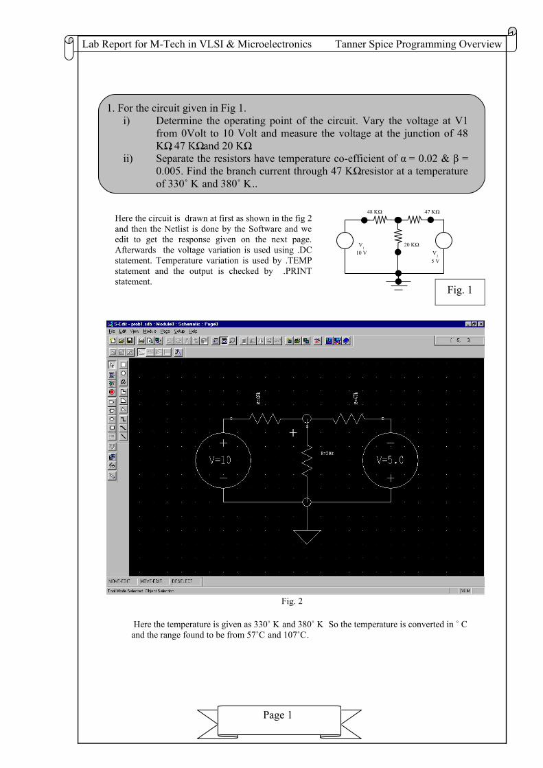
1. For the circuit given in Fig 1. i) Determine the operating point of the circuit. Vary the voltage at V1
from 0Volt to 10 Volt and measure the voltage at the junction of 48 KΩ, 47 KΩ and 20 KΩ.
ii) Separate the resistors have temperature co-efficient of α = 0.02 & β = 0.005. Find the branch current through 47 KΩ resistor at a temperature of 330˚ K and 380˚ K..
Here the circuit is drawn at first as shown in the fig 2 and then the Netlist is done by the Software and we edit to get the response given on the next page. Afterwards the voltage variation is used using .DC statement. Temperature variation is used by .TEMP statement and the output is checked by .PRINT statement.
Fig. 2
Here the temperature is given as 330˚ K and 380˚ K So the temperature is converted in ˚ C and the range found to be from 57˚C and 107˚C.
Page 1
V1
10 V V2
5 V
47 KΩ48 KΩ
20 KΩ
Fig. 1
Lab Report for M-Tech in VLSI & Microelectronics Tanner Spice Programming Overview
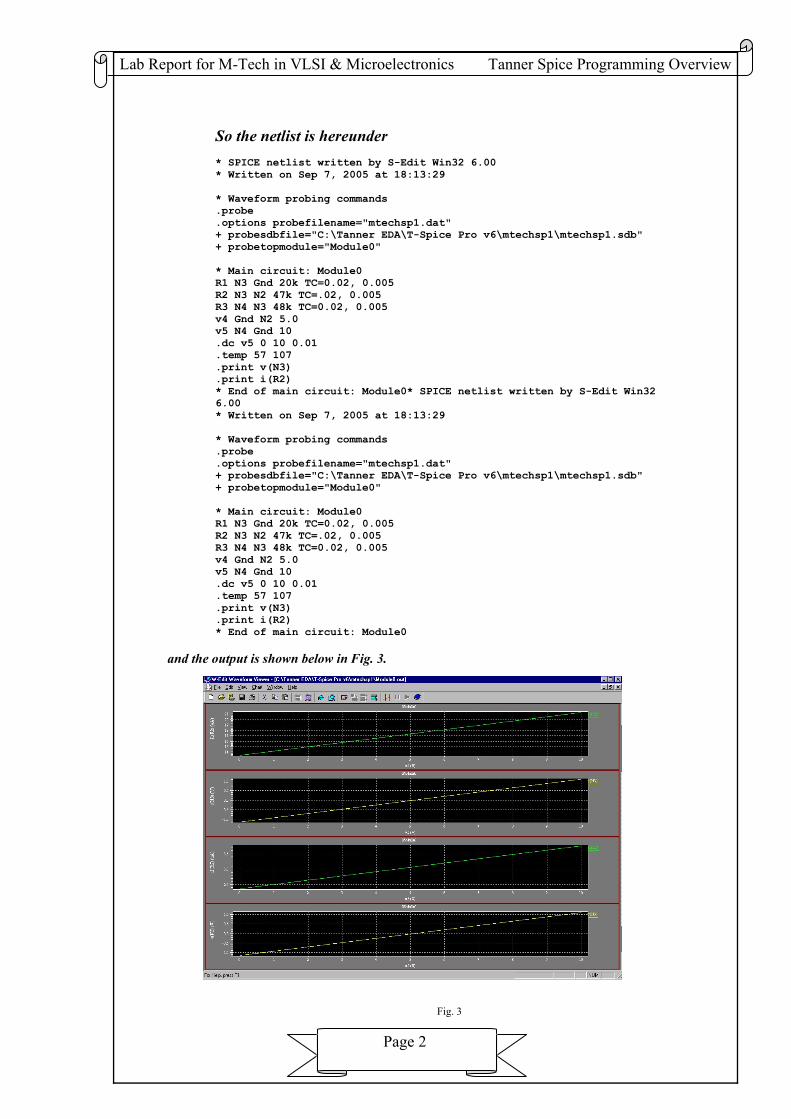
So the netlist is hereunder* SPICE netlist written by S-Edit Win32 6.00* Written on Sep 7, 2005 at 18:13:29* Waveform probing commands.probe.options probefilename="mtechsp1.dat"+ probesdbfile="C:\Tanner EDA\T-Spice Pro v6\mtechsp1\mtechsp1.sdb"+ probetopmodule="Module0"* Main circuit: Module0R1 N3 Gnd 20k TC=0.02, 0.005R2 N3 N2 47k TC=.02, 0.005R3 N4 N3 48k TC=0.02, 0.005v4 Gnd N2 5.0v5 N4 Gnd 10.dc v5 0 10 0.01.temp 57 107.print v(N3).print i(R2)* End of main circuit: Module0* SPICE netlist written by S-Edit Win32 6.00* Written on Sep 7, 2005 at 18:13:29* Waveform probing commands.probe.options probefilename="mtechsp1.dat"+ probesdbfile="C:\Tanner EDA\T-Spice Pro v6\mtechsp1\mtechsp1.sdb"+ probetopmodule="Module0"* Main circuit: Module0R1 N3 Gnd 20k TC=0.02, 0.005R2 N3 N2 47k TC=.02, 0.005R3 N4 N3 48k TC=0.02, 0.005v4 Gnd N2 5.0v5 N4 Gnd 10.dc v5 0 10 0.01.temp 57 107.print v(N3).print i(R2)* End of main circuit: Module0
and the output is shown below in Fig. 3.
Fig. 3
Page 2
Lab Report for M-Tech in VLSI & Microelectronics Tanner Spice Programming Overview
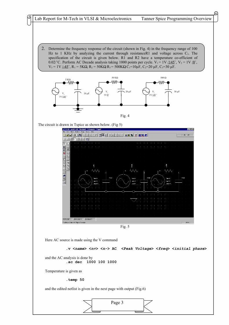
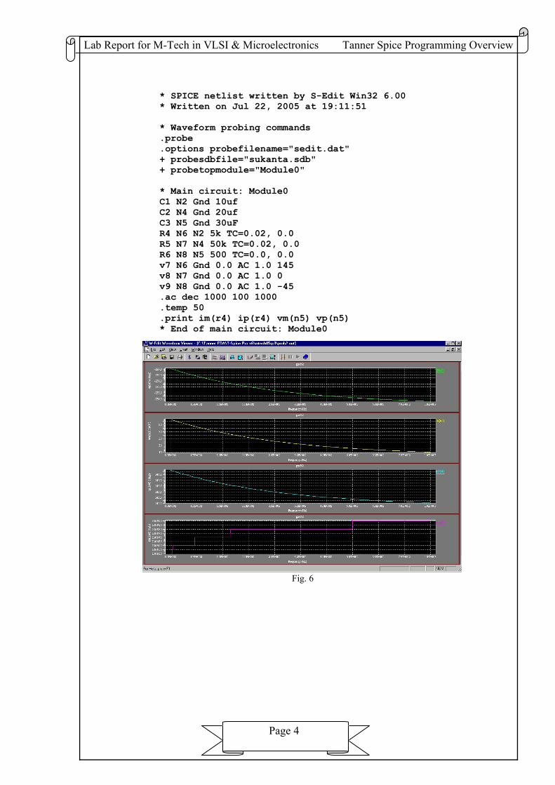
2. Determine the frequency response of the circuit (shown in Fig. 4) in the frequency range of 100 Hz to 1 KHz by analyzing the current through resistanceR1 and voltage across C3. The specification of the circuit is given below. R1 and R2 have a temperature co-efficient of 0.02/˚C. Perform AC Decade analysis taking 1000 points per cycle. V1 = 1V /145˚, V2 = 1V /0˚, V3 = 1V /-45˚, R1 = 5KΩ , R2 = 50KΩ, R3 = 500KΩ, C1=10μF, C2=20 μF, C3=30 μF.
Fig. 4
The circuit is drawn in Tspice as shown below. (Fig 5)
Fig. 5
Here AC source is made using the V command
.v <name> <n+> <n-> AC <Peak Voltage> <freq> <initial phaze> and the AC analysis is done by
.ac dec 1000 100 1000Temperature is given as
.temp 50and the edited netlist is given in the next page with output (Fig.6)
Page 3
V1
1V/145 ˚
5 KΩ
10 μFV
1
1V/-45 ˚ 20 μF
50 KΩ
30 μF
500 Ω
V1
1V/0˚
Lab Report for M-Tech in VLSI & Microelectronics Tanner Spice Programming Overview
* SPICE netlist written by S-Edit Win32 6.00* Written on Jul 22, 2005 at 19:11:51* Waveform probing commands.probe.options probefilename="sedit.dat"+ probesdbfile="sukanta.sdb"+ probetopmodule="Module0"* Main circuit: Module0C1 N2 Gnd 10ufC2 N4 Gnd 20ufC3 N5 Gnd 30uFR4 N6 N2 5k TC=0.02, 0.0R5 N7 N4 50k TC=0.02, 0.0R6 N8 N5 500 TC=0.0, 0.0v7 N6 Gnd 0.0 AC 1.0 145v8 N7 Gnd 0.0 AC 1.0 0v9 N8 Gnd 0.0 AC 1.0 -45.ac dec 1000 100 1000.temp 50.print im(r4) ip(r4) vm(n5) vp(n5) * End of main circuit: Module0
Fig. 6
Page 4
Lab Report for M-Tech in VLSI & Microelectronics Tanner Spice Programming Overview
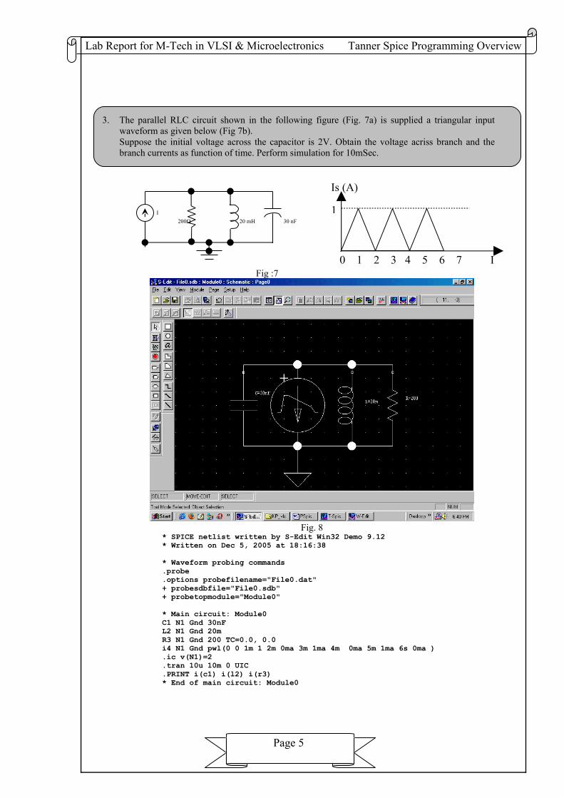
3. The parallel RLC circuit shown in the following figure (Fig. 7a) is supplied a triangular input waveform as given below (Fig 7b).Suppose the initial voltage across the capacitor is 2V. Obtain the voltage acriss branch and the branch currents as function of time. Perform simulation for 10mSec.
Fig :7
Fig. 8* SPICE netlist written by S-Edit Win32 Demo 9.12* Written on Dec 5, 2005 at 18:16:38* Waveform probing commands.probe.options probefilename="File0.dat"+ probesdbfile="File0.sdb"+ probetopmodule="Module0"* Main circuit: Module0C1 N1 Gnd 30nFL2 N1 Gnd 20mR3 N1 Gnd 200 TC=0.0, 0.0i4 N1 Gnd pwl(0 0 1m 1 2m 0ma 3m 1ma 4m 0ma 5m 1ma 6s 0ma ).ic v(N1)=2.tran 10u 10m 0 UIC.PRINT i(c1) i(l2) i(r3) * End of main circuit: Module0
Page 5
I 200Ω 30 nF20 mH
0 1 2 3 4 5 6 7 I
Is (A)
1
Lab Report for M-Tech in VLSI & Microelectronics Tanner Spice Programming Overview
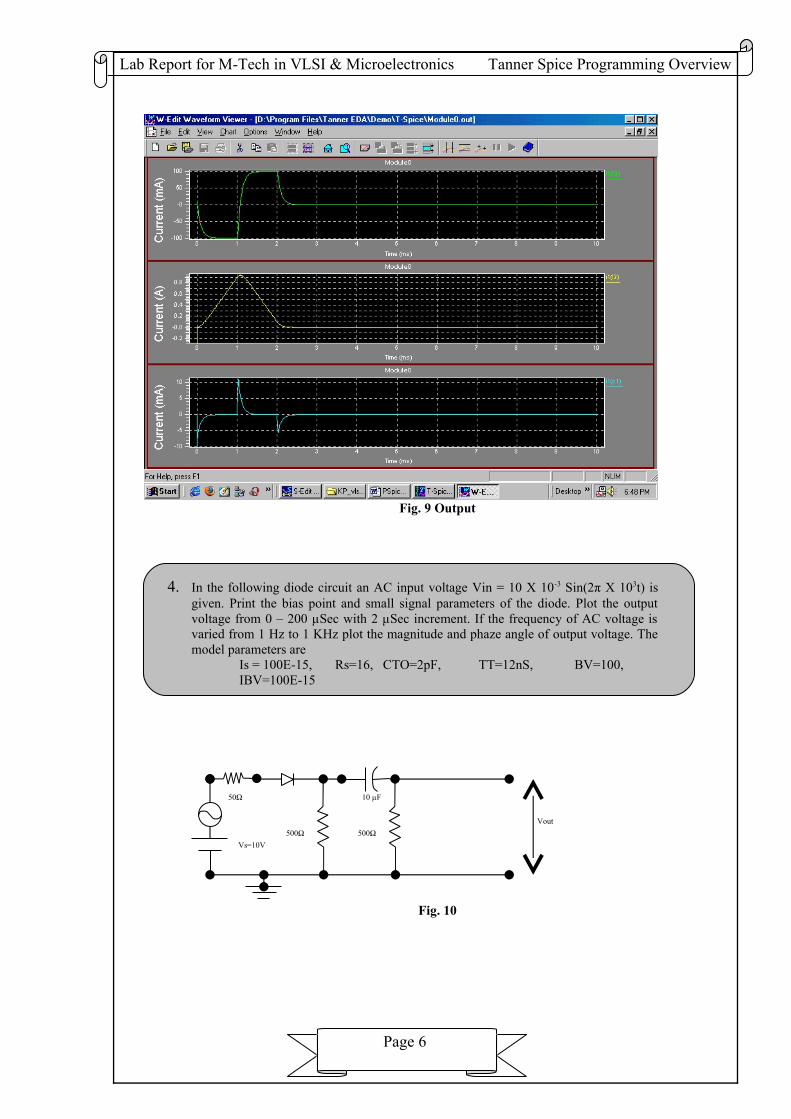
Fig. 9 Output
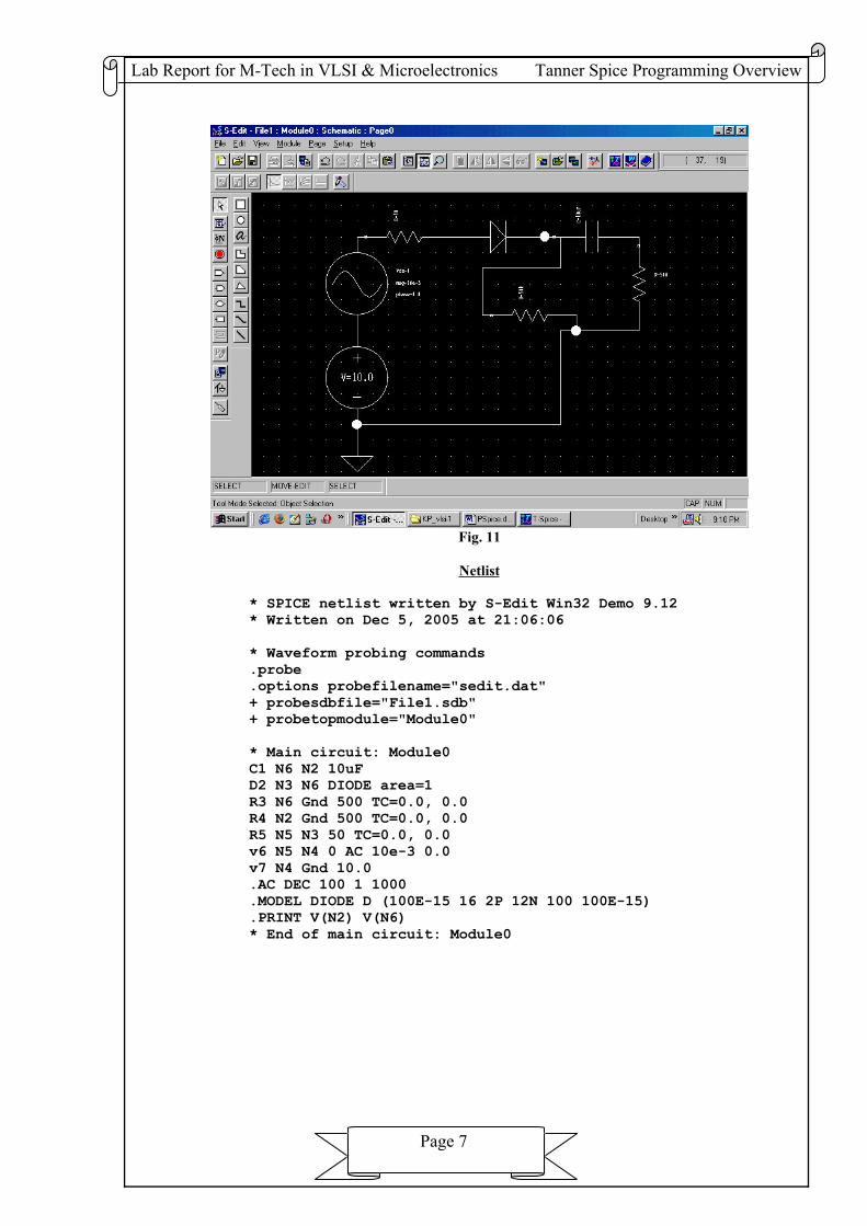
4. In the following diode circuit an AC input voltage Vin = 10 X 10-3 Sin(2π X 103t) is given. Print the bias point and small signal parameters of the diode. Plot the output voltage from 0 – 200 μSec with 2 μSec increment. If the frequency of AC voltage is varied from 1 Hz to 1 KHz plot the magnitude and phaze angle of output voltage. The model parameters are
Is = 100E-15, Rs=16, CTO=2pF, TT=12nS, BV=100,IBV=100E-15
Fig. 10
Page 6
50Ω 10 μF
500ΩVs=10V
500ΩVout
Lab Report for M-Tech in VLSI & Microelectronics Tanner Spice Programming Overview
Fig. 11
Netlist
* SPICE netlist written by S-Edit Win32 Demo 9.12* Written on Dec 5, 2005 at 21:06:06* Waveform probing commands.probe.options probefilename="sedit.dat"+ probesdbfile="File1.sdb"+ probetopmodule="Module0"* Main circuit: Module0C1 N6 N2 10uFD2 N3 N6 DIODE area=1R3 N6 Gnd 500 TC=0.0, 0.0R4 N2 Gnd 500 TC=0.0, 0.0R5 N5 N3 50 TC=0.0, 0.0v6 N5 N4 0 AC 10e-3 0.0v7 N4 Gnd 10.0.AC DEC 100 1 1000.MODEL DIODE D (100E-15 16 2P 12N 100 100E-15).PRINT V(N2) V(N6)* End of main circuit: Module0
Page 7
Lab Report for M-Tech in VLSI & Microelectronics Tanner Spice Programming Overview
Output:
Fig. 12
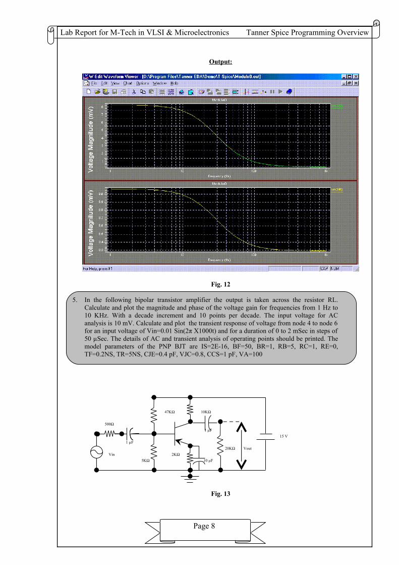
5. In the following bipolar transistor amplifier the output is taken across the resistor RL. Calculate and plot the magnitude and phase of the voltage gain for frequencies from 1 Hz to 10 KHz. With a decade increment and 10 points per decade. The input voltage for AC analysis is 10 mV. Calculate and plot the transient response of voltage from node 4 to node 6 for an input voltage of Vin=0.01 Sin(2π X1000t) and for a duration of 0 to 2 mSec in steps of 50 μSec. The details of AC and transient analysis of operating points should be printed. The model parameters of the PNP BJT are IS=2E-16, BF=50, BR=1, RB=5, RC=1, RE=0, TF=0.2NS, TR=5NS, CJE=0.4 pF, VJC=0.8, CCS=1 pF, VA=100
Fig. 13
Page 8
1 μF
10KΩ
Vout2KΩ
20KΩ
47KΩ
5KΩ
500Ω
Vin10 μF
1 μF15 V
Lab Report for M-Tech in VLSI & Microelectronics Tanner Spice Programming Overview
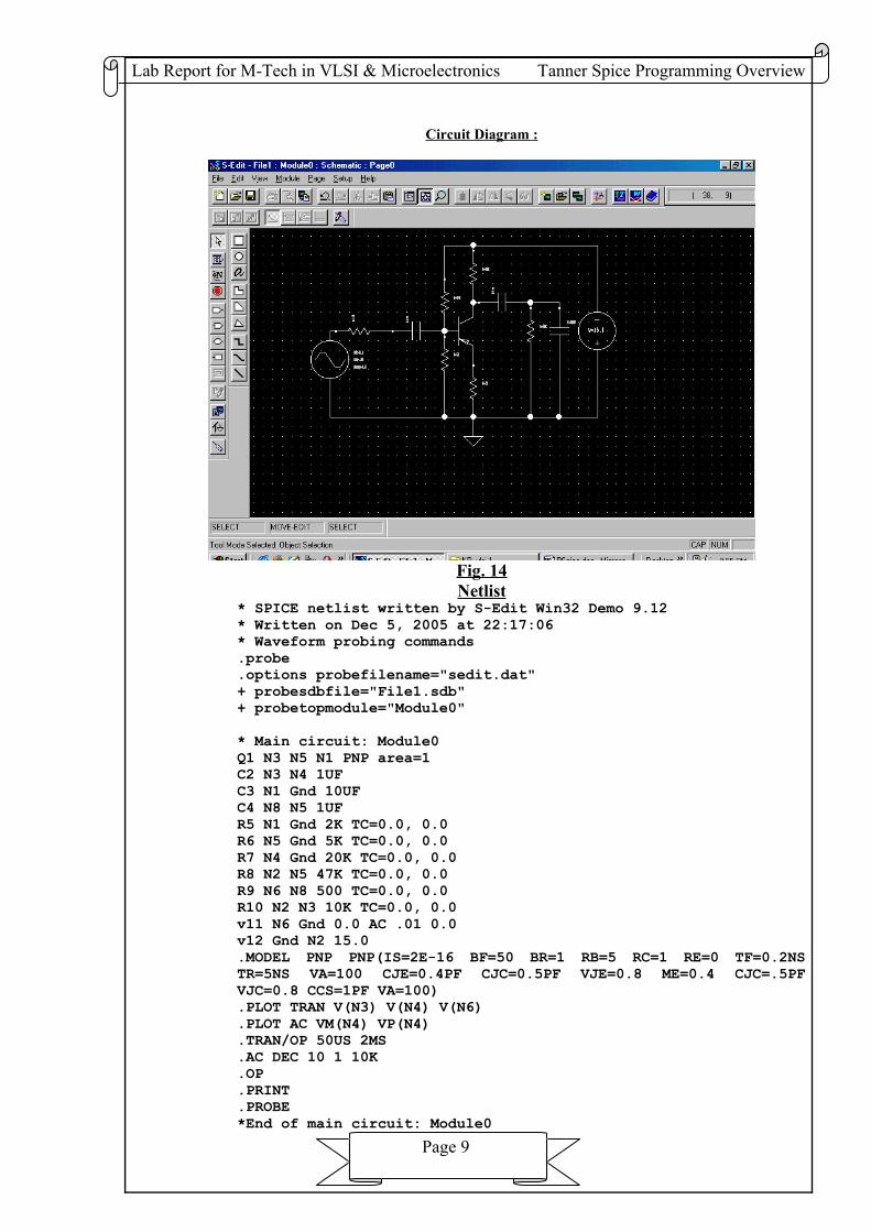
Circuit Diagram :
Fig. 14Netlist
* SPICE netlist written by S-Edit Win32 Demo 9.12* Written on Dec 5, 2005 at 22:17:06* Waveform probing commands.probe.options probefilename="sedit.dat"+ probesdbfile="File1.sdb"+ probetopmodule="Module0"* Main circuit: Module0Q1 N3 N5 N1 PNP area=1C2 N3 N4 1UFC3 N1 Gnd 10UFC4 N8 N5 1UFR5 N1 Gnd 2K TC=0.0, 0.0R6 N5 Gnd 5K TC=0.0, 0.0R7 N4 Gnd 20K TC=0.0, 0.0R8 N2 N5 47K TC=0.0, 0.0R9 N6 N8 500 TC=0.0, 0.0R10 N2 N3 10K TC=0.0, 0.0v11 N6 Gnd 0.0 AC .01 0.0v12 Gnd N2 15.0.MODEL PNP PNP(IS=2E-16 BF=50 BR=1 RB=5 RC=1 RE=0 TF=0.2NS TR=5NS VA=100 CJE=0.4PF CJC=0.5PF VJE=0.8 ME=0.4 CJC=.5PF VJC=0.8 CCS=1PF VA=100) .PLOT TRAN V(N3) V(N4) V(N6).PLOT AC VM(N4) VP(N4).TRAN/OP 50US 2MS.AC DEC 10 1 10K.OP.PRINT .PROBE*End of main circuit: Module0
Page 9
Lab Report for M-Tech in VLSI & Microelectronics Tanner Spice Programming Overview
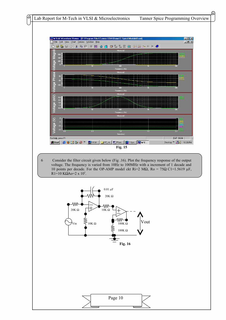
Fig. 15
6 Consider the filter circuit given below (Fig .16). Plot the frequency response of the output voltage. The frequency is varied from 10Hz to 100MHz with a increment of 1 decade and 10 points per decade. For the OP-AMP model ckt Ri=2 MΩ , Ro = 75Ω, C1=1.5619 μF, R1=10 KΩ Ao=2 x 10⁵.
Fig. 16
Page 10
Vout100K Ω
100K Ω
10K Ω
20K Ω
20K Ω
Vin
0.01 μF
10K Ω
Lab Report for M-Tech in VLSI & Microelectronics Tanner Spice Programming Overview
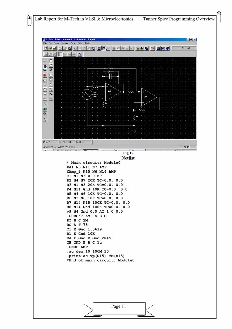
Fig 17Netlist
* Main circuit: Module0XA1 N3 N11 N7 AMPXAmp_2 N15 N6 N14 AMPC1 N1 N3 0.01uFR2 N4 N7 20K TC=0.0, 0.0R3 N1 N3 20K TC=0.0, 0.0R4 N11 Gnd 10K TC=0.0, 0.0R5 N4 N6 10K TC=0.0, 0.0R6 N3 N6 10K TC=0.0, 0.0R7 N14 N15 100K TC=0.0, 0.0R8 N14 Gnd 100K TC=0.0, 0.0v9 N4 Gnd 0.0 AC 1.0 0.0.SUBCKT AMP A B CRI B C 2MRO A F 75C1 E Gnd 1.5619R1 E Gnd 10KEA F Gnd E Gnd 2E+5GB GND E B C 1u.ENDS AMP.ac dec 10 100M 10.print ac vp(N15) VM(n15)*End of main circuit: Module0
Page 11
Lab Report for M-Tech in VLSI & Microelectronics Tanner Spice Programming Overview
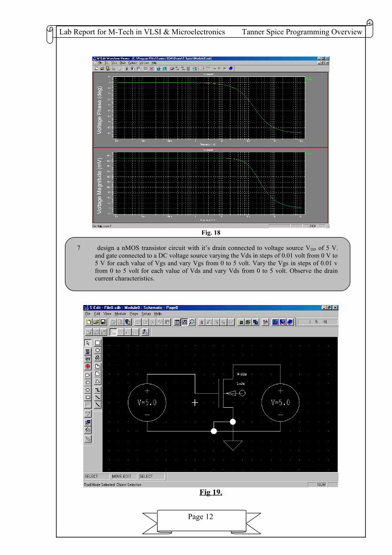
Fig. 18
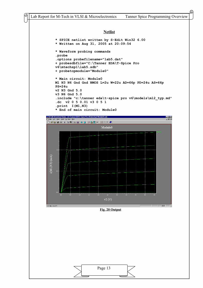
7 design a nMOS transistor circuit with it’s drain connected to voltage source VDD of 5 V. and gate connected to a DC voltage source varying the Vds in steps of 0.01 volt from 0 V to 5 V for each value of Vgs and vary Vgs from 0 to 5 volt. Vary the Vgs in steps of 0.01 v from 0 to 5 volt for each value of Vds and vary Vds from 0 to 5 volt. Observe the drain current characteristics.
Fig 19.
Page 12
Lab Report for M-Tech in VLSI & Microelectronics Tanner Spice Programming Overview
Netlist
* SPICE netlist written by S-Edit Win32 6.00* Written on Aug 31, 2005 at 20:09:54* Waveform probing commands.probe.options probefilename="lab5.dat"+ probesdbfile="C:\Tanner EDA\T-Spice Pro v6\mtechsp1\lab5.sdb"+ probetopmodule="Module0"* Main circuit: Module0M1 N3 N6 Gnd Gnd NMOS L=2u W=22u AD=66p PD=24u AS=66p PS=24u v2 N3 Gnd 5.0v3 N6 Gnd 5.0.include "c:\tanner eda\t-spice pro v6\models\ml2_typ.md".dc v2 0 5 0.01 v3 0 5 1.print I(M1,N3)* End of main circuit: Module0
Fig. 20 Output
Page 13
Lab Report for M-Tech in VLSI & Microelectronics Tanner Spice Programming Overview
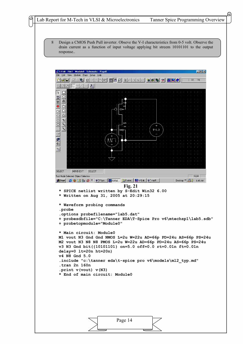
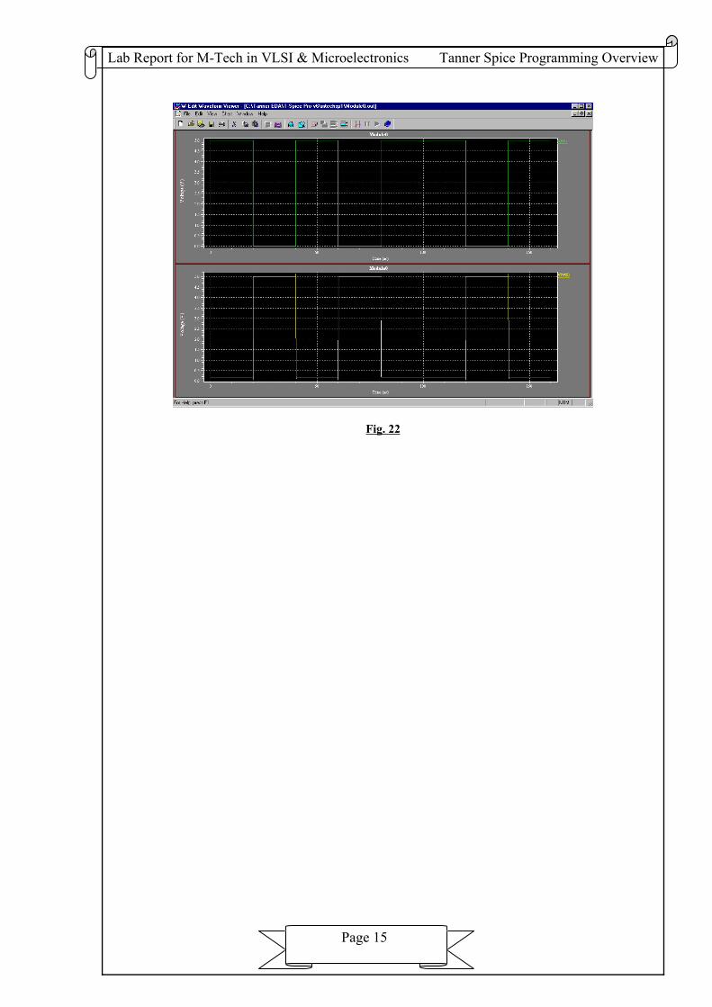
8 Design a CMOS Push Pull inverter. Obseve the V-I characteristics from 0-5 volt. Observe the drain current as a function of input voltage applying bit streem 10101101 to the output response..
Fig. 21* SPICE netlist written by S-Edit Win32 6.00* Written on Aug 31, 2005 at 20:29:15* Waveform probing commands.probe.options probefilename="lab5.dat"+ probesdbfile="C:\Tanner EDA\T-Spice Pro v6\mtechsp1\lab5.sdb"+ probetopmodule="Module0"* Main circuit: Module0M1 vout N3 Gnd Gnd NMOS L=2u W=22u AD=66p PD=24u AS=66p PS=24u M2 vout N3 N8 N8 PMOS L=2u W=22u AD=66p PD=24u AS=66p PS=24uv3 N3 Gnd bit(10101101 on=5.0 off=0.0 rt=0.01n ft=0.01n delay=0 lt=20n ht=20n)v4 N8 Gnd 5.0.include "c:\tanner eda\t-spice pro v6\models\ml2_typ.md".tran 2n 160n.print v(vout) v(N3) * End of main circuit: Module0
Page 14
Lab Report for M-Tech in VLSI & Microelectronics Tanner Spice Programming Overview
Fig. 22
Page 15