Fузыкальный инструмент « Kкрипка» · > ? i : j l : f ? g l d m eЬ l m jЫ = h j h > f h k d
Read Chapter 3 of “Principles of Power Electronics” (KSV) by J. G. Kassakian, M.
F. Schlecht, and G. C. Verghese, Addison-Wesley, 1991.
Start with simple half-wave rectifier (full-bridge rectifier directly follows).
Ld + −
Id VxD1 id+ + ω t
VoVsSin(ωt) D2 Vx π 2π −− VsSin(ωt)
D1 ON D2 ON
Figure 2.1: Simple Half-wave Rectifier
In P.S.S.:
< vo > = < vx >
vs = (2.1)
π
10
vsIf Ld Big → id ≃ Id =
πR (2.2)
If LR d ≫ 2
ωπ ⇒ we can approximate load as a constant current.
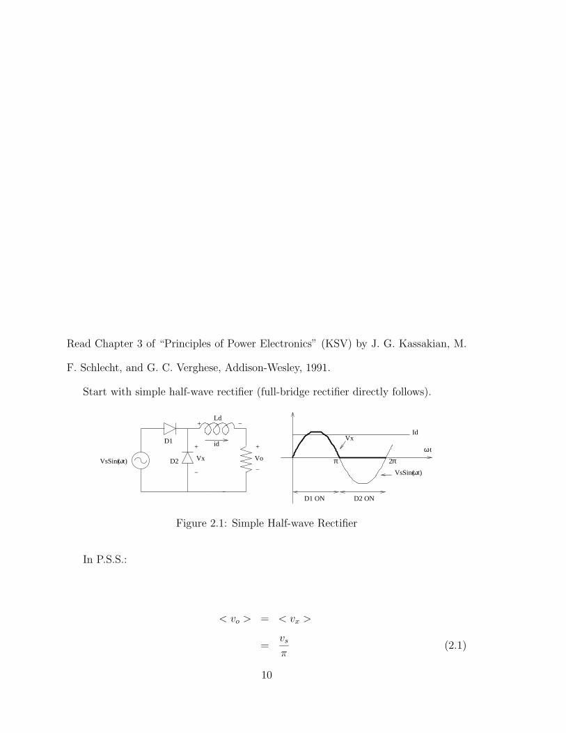
2.1 Load Regulation
.Now consider adding some ac-side inductance Lc (reactance Xc = ωLc).
• Common situation: Transformer leakage or line inductance, machine winding
inductance, etc.
• Lc is typically ≪ Ld (filter inductance) as it is a parasitic element.
Lc Ld
D1 +
RVsSin(ωt) D2 Vx
−
Figure 2.2: Adding Some AC-Side Inductance
Assume Ld ∼ ∞ (so ripple current is small). Therefore, we can approximate load
as a “special” current source.
vx“Special” since < vL >= 0 in P.S.S. Id =< > (2.3) ⇒
R
Assume we start with D2 conducting, D1 off (V sin(ωt) < 0). What happens when
V sin(ωt) crosses zero?
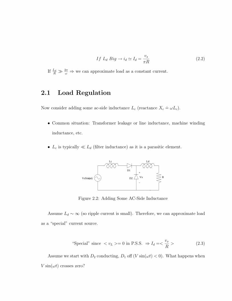
i1 Lc
D1
VsSin(ωt) D2 i2 Id
Figure 2.3: Special Current
• D1 off no longer valid.
But just after turn on i1 still = 0.•
Therefore, D1
switches from D2
and D2
to D1.
are both on d
Lc
uring a commutation period, where current
i1
D1
+
VsSin( ω t) D2 Vx Id _
i2
Figure 2.4: Commutation Period
D2 will stay on as long as i2 > 0 (i1 < Id).
Analyze:
di1 1 = Vs sin(ωt)
dt Lc ∫ ωt Vs
i1(t) = sin(ωt)d(ωt) 0 ωLc
Vs 0 = ωLc
cos(Φ)|ωt
Vs = [1 − cos(ωt)] (2.4)
ωLc
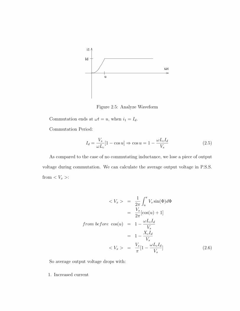
i1
u
Id
tω
Figure 2.5: Analyze Waveform
Commutation ends at ωt = u, when i1 = Id.
Commutation Period:
Vs ωLcIdId =
ωLc [1 − cos u] ⇒ cos u = 1 −
Vs (2.5)
As compared to the case of no commutating inductance, we lose a piece of output
voltage during commutation. We can calculate the average output voltage in P.S.S.
from < Vx >:
1 ∫ π < Vx > = Vs sin(Φ)dΦ
2π u
Vs = [cos(u) + 1]
2π ωLcId
from before cos(u) = 1 − Vs
XcId = 1 −
Vs
Vs ωLcId< Vx > = [1 − ] (2.6)
π Vs
So average output voltage drops with:
1. Increased current
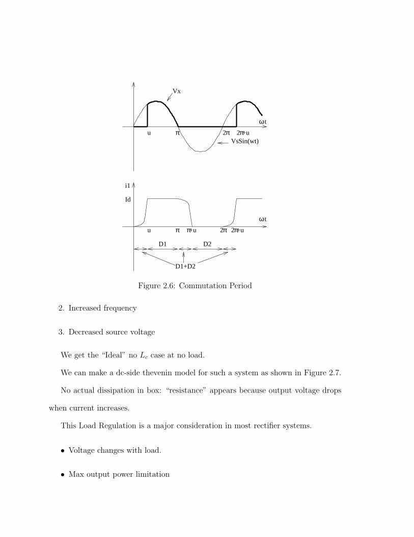
πu VsSin(wt)
Vx
ω t
π+u2π2
i1
Id
ω t
u +u 2 +u
D1 D2
π π π2π
D1+D2
Figure 2.6: Commutation Period
2. Increased frequency
3. Decreased source voltage
We get the “Ideal” no Lc case at no load.
We can make a dc-side thevenin model for such a system as shown in Figure 2.7.
No actual dissipation in box: “resistance” appears because output voltage drops
when current increases.
This Load Regulation is a major consideration in most rectifier systems.
• Voltage changes with load.
• Max output power limitation
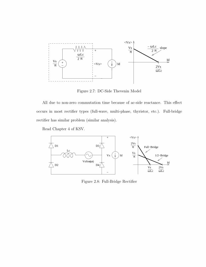
Id
+
<Vx>
<Vx>
Id
2 π slope
2 π Lcω
ω Lc
2Vs Lcω
− +
−
π Vs
−
π Vs
Figure 2.7: DC-Side Thevenin Model
All due to non-zero commutation time because of ac-side reactance.
occurs in most rectifier types (full-wave, multi-phase, thyristor, etc.).
rectifier has similar problem (similar analysis).
Read Chapter 4 of KSV.
This effect
Full-bridge
+ <Vx>
D3
D2
D1
D4 ωVsSin( t)
Lc
2Vs π Full−Bridge
Vs Vx Id π 1/2−Bridge
Id
Vs 2Vs ω Lc ω Lc−
Figure 2.8: Full-Bridge Rectifier


![Ba^QdPc E RPW lPMcW^] - Farnell element145 P^\_McWOWZWch 5 § 5 @^ §@^ BVhbWPMZ EWjR HI g : g 5 I \\ ?MW] J J 7a^]c E_RMYRa J J 4R]cRa E_RMYRa J J DRMa E_RMYRa J J EdOf^^SRa g g 5WbP](https://static.fdocument.org/doc/165x107/5f62e0104f48cc34e33e05f9/baqdpc-e-rpw-lpmcw-farnell-5-pmcwowzwch-5-5-bvhbwpmz-ewjr-hi.jpg)