Kobe University Particle Physics Labo. MPGD (μ …pp Physics labo. MPGD (μ-PIC) group ATLAS...
27
Kobe University Particle Physics Labo. MPGD (μ-PIC) group 29/08/2014 KUBEC International workshop on DM search Atsuhiko Ochi
Transcript of Kobe University Particle Physics Labo. MPGD (μ …pp Physics labo. MPGD (μ-PIC) group ATLAS...
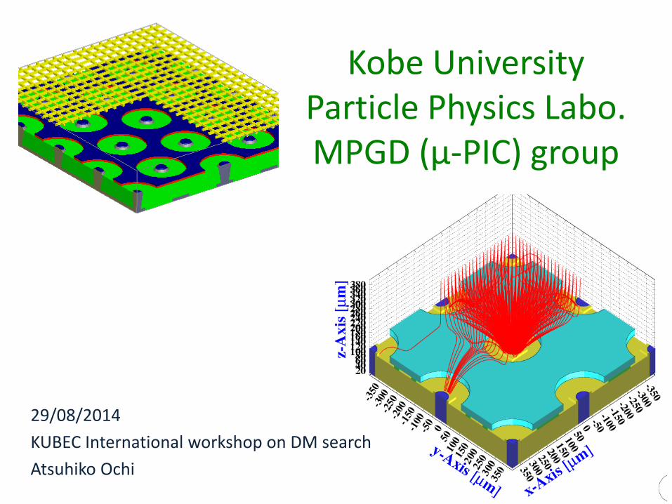
Kobe UniversityParticle Physics Labo.MPGD (μ-PIC) group
29/08/2014
KUBEC International workshop on DM search
Atsuhiko Ochi
-800 V
-550 VConversion & drift space
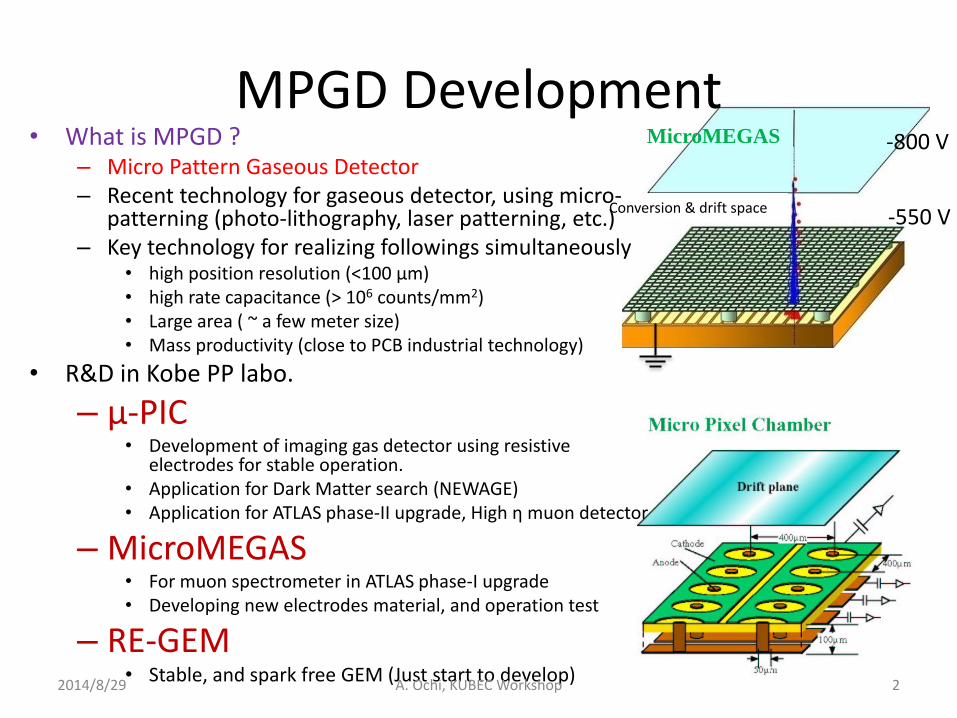
MicroMEGAS• What is MPGD ?– Micro Pattern Gaseous Detector– Recent technology for gaseous detector, using micro-
patterning (photo-lithography, laser patterning, etc.)– Key technology for realizing followings simultaneously
• high position resolution (<100 μm)• high rate capacitance (> 106 counts/mm2)• Large area ( ~ a few meter size) • Mass productivity (close to PCB industrial technology)
• R&D in Kobe PP labo.
– μ-PIC• Development of imaging gas detector using resistive
electrodes for stable operation.• Application for Dark Matter search (NEWAGE)• Application for ATLAS phase-II upgrade, High η muon detector
– MicroMEGAS• For muon spectrometer in ATLAS phase-I upgrade• Developing new electrodes material, and operation test
– RE-GEM• Stable, and spark free GEM (Just start to develop)
MPGD Development
2014/8/29 2A. Ochi, KUBEC Workshop
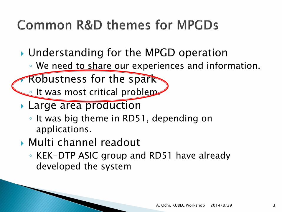
Understanding for the MPGD operation◦ We need to share our experiences and information.
Robustness for the spark◦ It was most critical problem.
Large area production◦ It was big theme in RD51, depending on
applications.
Multi channel readout◦ KEK-DTP ASIC group and RD51 have already
developed the system
2014/8/29A. Ochi, KUBEC Workshop 3

2014/8/29A. Ochi, KUBEC Workshop 4
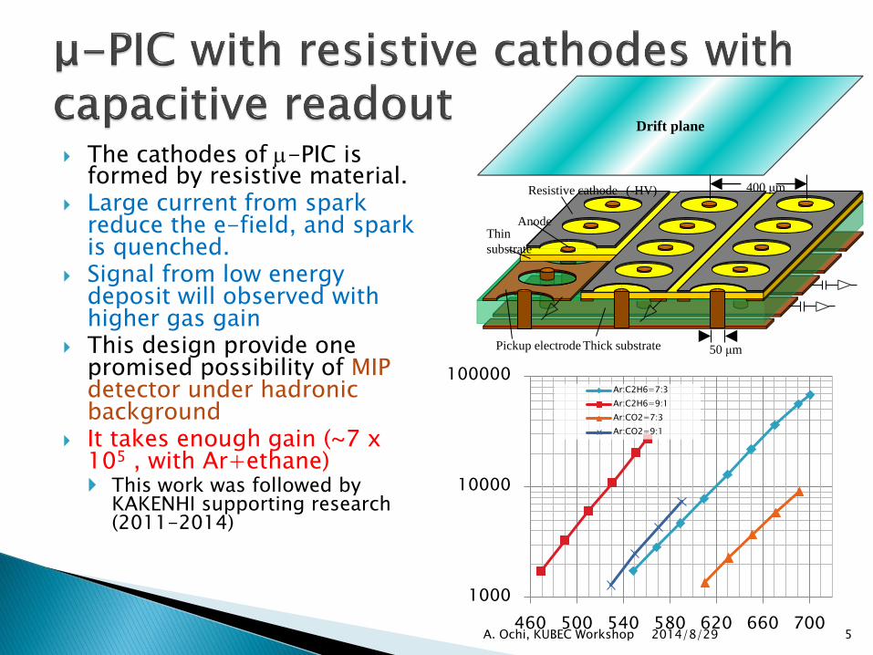
The cathodes of m-PIC is formed by resistive material.
Large current from spark reduce the e-field, and spark is quenched.
Signal from low energy deposit will observed with higher gas gain
This design provide one promised possibility of MIP detector under hadronicbackground
It takes enough gain (~7 x 10⁵ , with Ar+ethane) This work was followed by
KAKENHI supporting research (2011-2014)
2014/8/29A. Ochi, KUBEC Workshop 5
Drift plane
Anode
Resistive cathode (-HV)
Pickup electrode
Thin
substrate
400 μm
Thick substrate 50 μm
1000
10000
100000
460 500 540 580 620 660 700
Ar:C2H6=7:3
Ar:C2H6=9:1
Ar:CO2=7:3
Ar:CO2=9:1
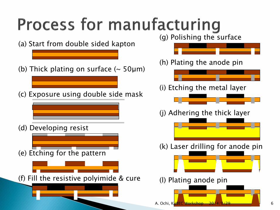
(a) Start from double sided kapton
(b) Thick plating on surface (~ 50μm)
(c) Exposure using double side mask
(d) Developing resist
(e) Etching for the pattern
(f) Fill the resistive polyimide & cure
(g) Polishing the surface
(h) Plating the anode pin
(i) Etching the metal layer
(j) Adhering the thick layer
(k) Laser drilling for anode pin
(l) Plating anode pin
2014/8/29A. Ochi, KUBEC Workshop 6
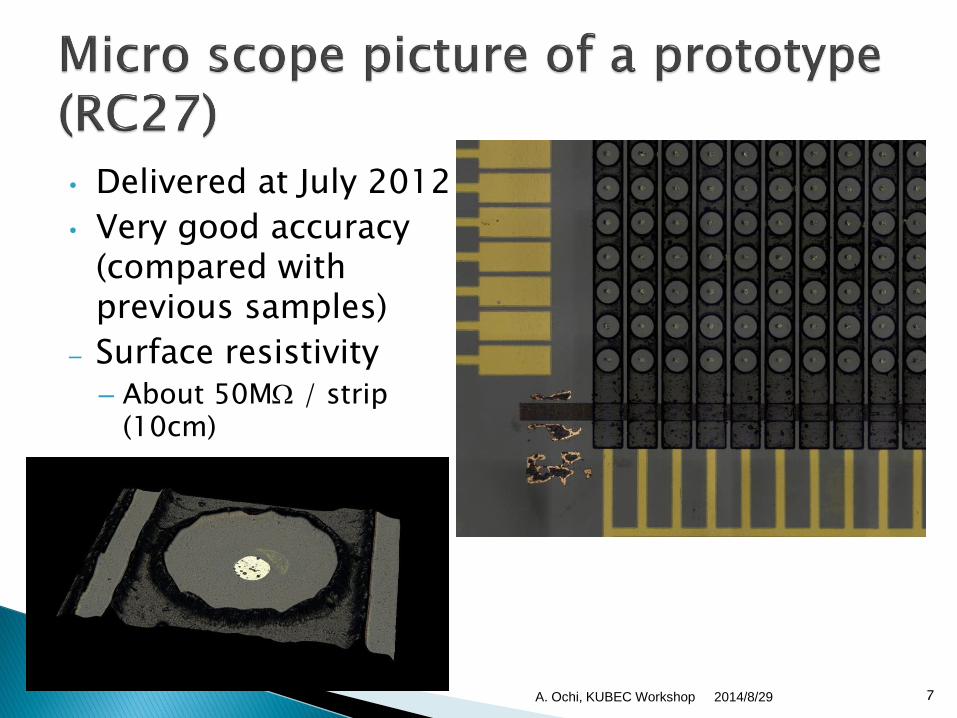
• Delivered at July 2012
• Very good accuracy (compared with previous samples)
– Surface resistivity– About 50MW / strip
(10cm)
2014/8/29A. Ochi, KUBEC Workshop 7
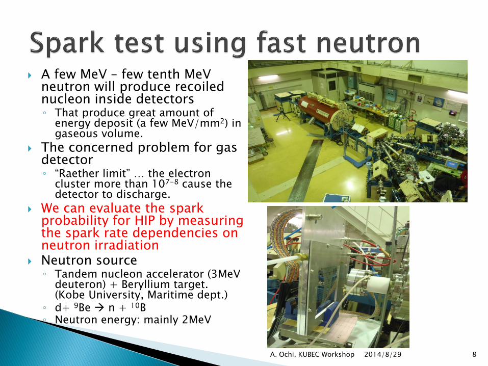
A few MeV – few tenth MeVneutron will produce recoiled nucleon inside detectors◦ That produce great amount of
energy deposit (a few MeV/mm2) in gaseous volume.
The concerned problem for gas detector◦ “Raether limit” … the electron
cluster more than 107-8 cause the detector to discharge.
We can evaluate the spark probability for HIP by measuring the spark rate dependencies on neutron irradiation
Neutron source◦ Tandem nucleon accelerator (3MeV
deuteron) + Beryllium target.(Kobe University, Maritime dept.)
◦ d+ 9Be n + 10B◦ Neutron energy: mainly 2MeV
2014/8/29A. Ochi, KUBEC Workshop 8
2014/8/29A. Ochi, KUBEC Workshop 9
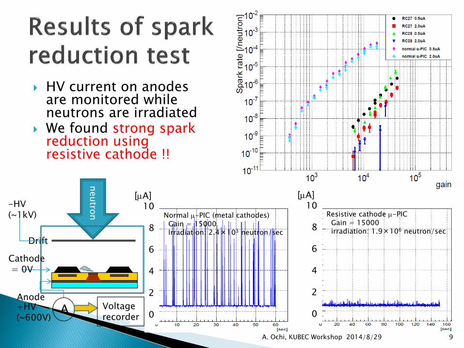
HV current on anodes are monitored while neutrons are irradiated
We found strong spark reduction using resistive cathode !!
Normal m-PIC (metal cathodes)Gain = 15000Irradiation: 2.4×10³ neutron/sec
Resistive cathode m-PIC Gain = 15000irradiation: 1.9×10⁶ neutron/sec
[mA]10
8
6
4
2
0
[mA]10
8
6
4
2
0
neutro
n
Drift
-HV(~1kV)
Cathode= 0V
A+HV(~600V)
AnodeVoltage recorder
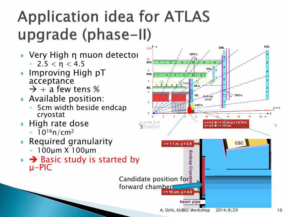
Very High η muon detector◦ 2.5 < η < 4.5
Improving High pTacceptance + a few tens %
Available position:◦ 5cm width beside endcap
cryostat
High rate dose◦ 1016n/cm2
Required granularity◦ 100μm X 100μm
Basic study is started by μ-PIC
Candidate position for forward chamber
2014/8/29 10A. Ochi, KUBEC Workshop
2014/8/29A. Ochi, KUBEC Workshop 11
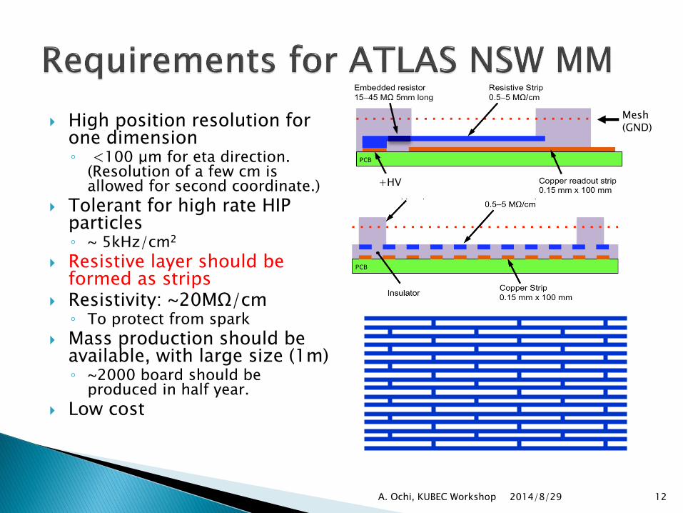
High position resolution for one dimension◦ <100 μm for eta direction.
(Resolution of a few cm is allowed for second coordinate.)
Tolerant for high rate HIP particles◦ ~ 5kHz/cm2
Resistive layer should be formed as strips
Resistivity: ~20MΩ/cm◦ To protect from spark
Mass production should be available, with large size (1m)◦ ~2000 board should be
produced in half year.
Low cost
2014/8/29A. Ochi, KUBEC Workshop 12
+HV
Mesh(GND)
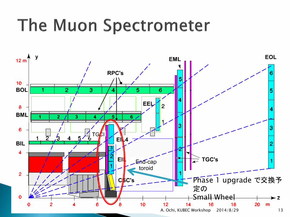
Phase 1 upgrade で交換予定のSmall Wheel
2014/8/29 13A. Ochi, KUBEC Workshop
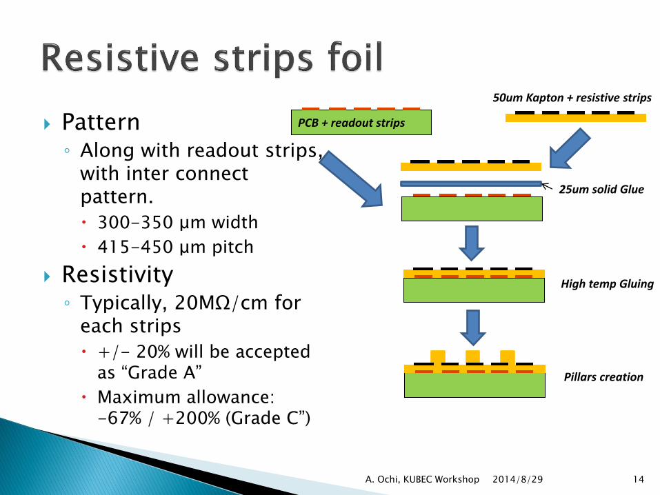
Pattern◦ Along with readout strips,
with inter connect pattern.
300-350 μm width
415-450 μm pitch
Resistivity◦ Typically, 20MΩ/cm for
each strips
+/- 20% will be accepted as “Grade A”
Maximum allowance:-67% / +200% (Grade C”)
2014/8/29A. Ochi, KUBEC Workshop 14
PCB + readout strips
50um Kapton + resistive strips
25um solid Glue
High temp Gluing
Pillars creation

Sputtering+liftoff◦ Pros.
Large area (>2m) Fine pattern (<100μm) Uniform resistivity Strong attachment on substrate
◦ Cons. Production speed
(Now, it will be OK, next slide) High cost
Screen printing◦ Pros.
Large area (>2m) Fast production speed Low cost for mass production
◦ Cons. Stability of resistivity Thick pattern (~20 μm) Lower tolerance for breakdown
for high voltage
2014/8/29A. Ochi, KUBEC Workshop 15
squeegee
frame
Screen ink stencil
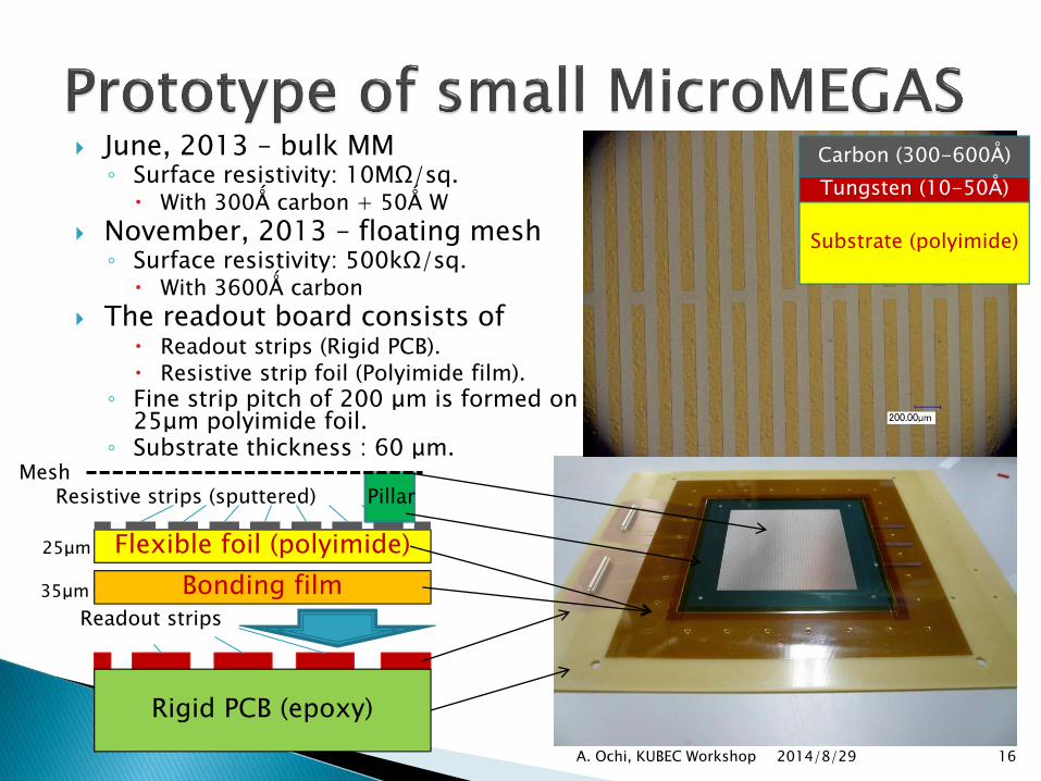
June, 2013 – bulk MM◦ Surface resistivity: 10MΩ/sq.
With 300Ǻ carbon + 50Ǻ W
November, 2013 – floating mesh◦ Surface resistivity: 500kΩ/sq.
With 3600Ǻ carbon
The readout board consists of Readout strips (Rigid PCB). Resistive strip foil (Polyimide film).
◦ Fine strip pitch of 200 μm is formed on 25μm polyimide foil.
◦ Substrate thickness : 60 μm.
2014/8/29A. Ochi, KUBEC Workshop 16
Flexible foil (polyimide)
Rigid PCB (epoxy)
Resistive strips (sputtered)
Readout strips
Bonding film
MeshPillar
25μm
35μm
Substrate (polyimide)
Carbon (300-600Å)
Tungsten (10-50Å)
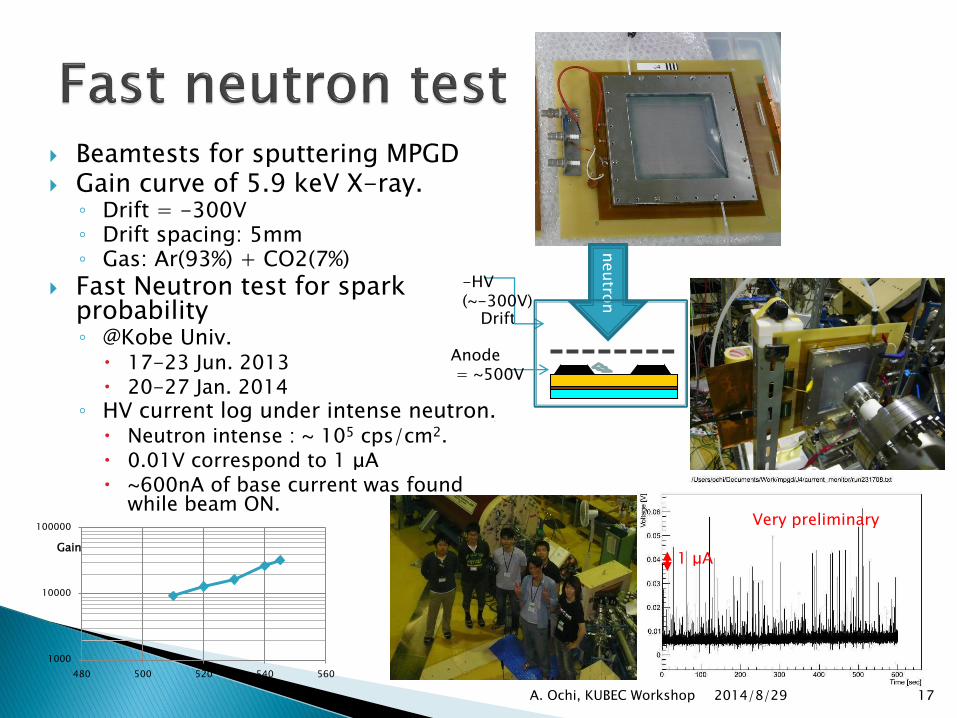
Beamtests for sputtering MPGD Gain curve of 5.9 keV X-ray.
◦ Drift = -300V◦ Drift spacing: 5mm◦ Gas: Ar(93%) + CO2(7%)
Fast Neutron test for spark probability◦ @Kobe Univ.
17-23 Jun. 2013 20-27 Jan. 2014
◦ HV current log under intense neutron. Neutron intense : ~ 105 cps/cm2. 0.01V correspond to 1 μA ~600nA of base current was found
while beam ON.
Be(d, n)B1000
10000
100000
480 500 520 540 560
Gain1 μA
Very preliminary
neutro
n
Drift
-HV(~-300V)
Anode= ~500V
A
2014/8/29A. Ochi, KUBEC Workshop 17
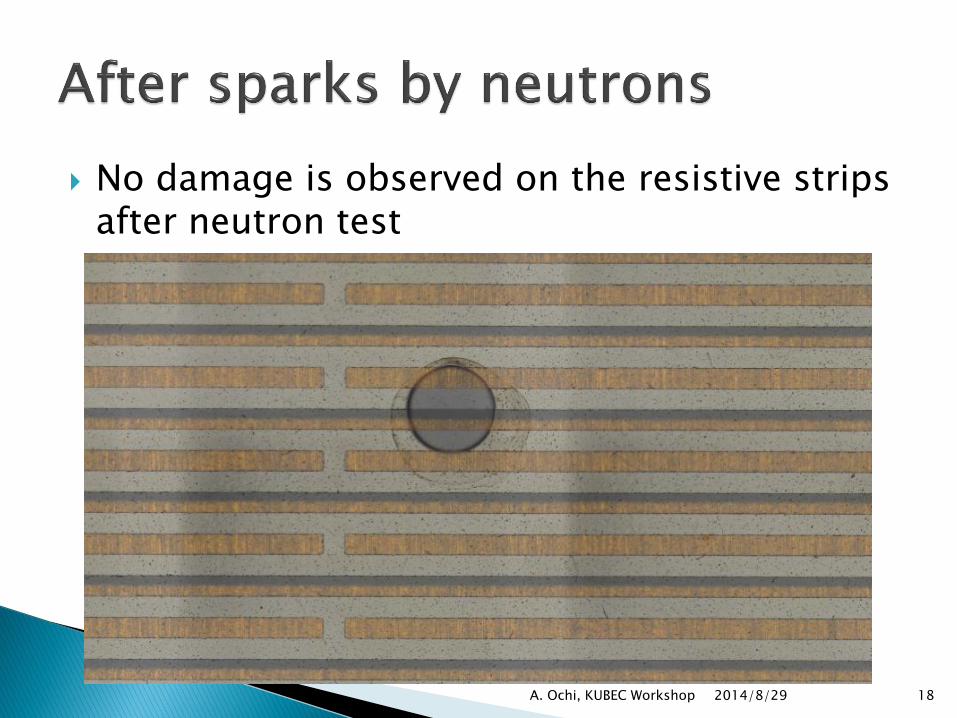
No damage is observed on the resistive strips after neutron test
2014/8/29A. Ochi, KUBEC Workshop 18
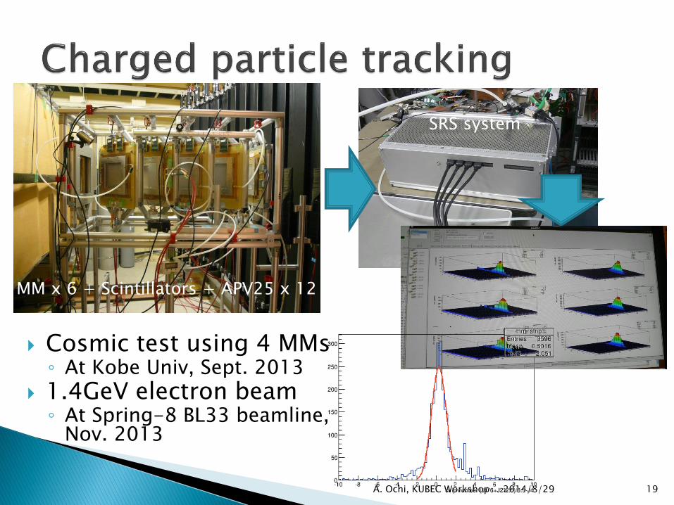
SRS system
Cosmic test using 4 MMs◦ At Kobe Univ, Sept. 2013
1.4GeV electron beam◦ At Spring-8 BL33 beamline,
Nov. 2013
2014/8/29A. Ochi, KUBEC Workshop 19
MM x 6 + Scintillators + APV25 x 12

2014/8/29A. Ochi, KUBEC Workshop 20
866.4mm
425.3mm
2014/8/29A. Ochi, KUBEC Workshop 21
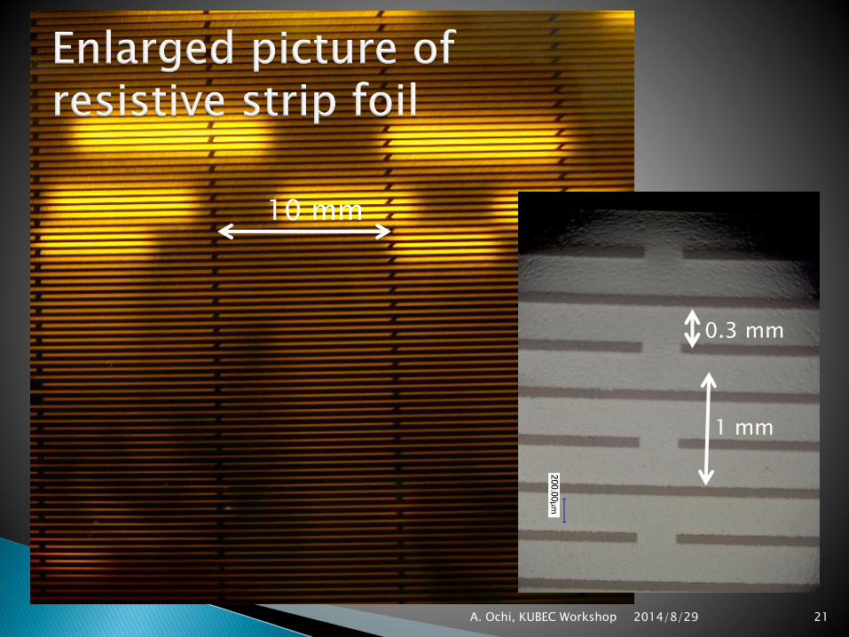
10 mm
1 mm
0.3 mm
2014/8/29A. Ochi, KUBEC Workshop 22
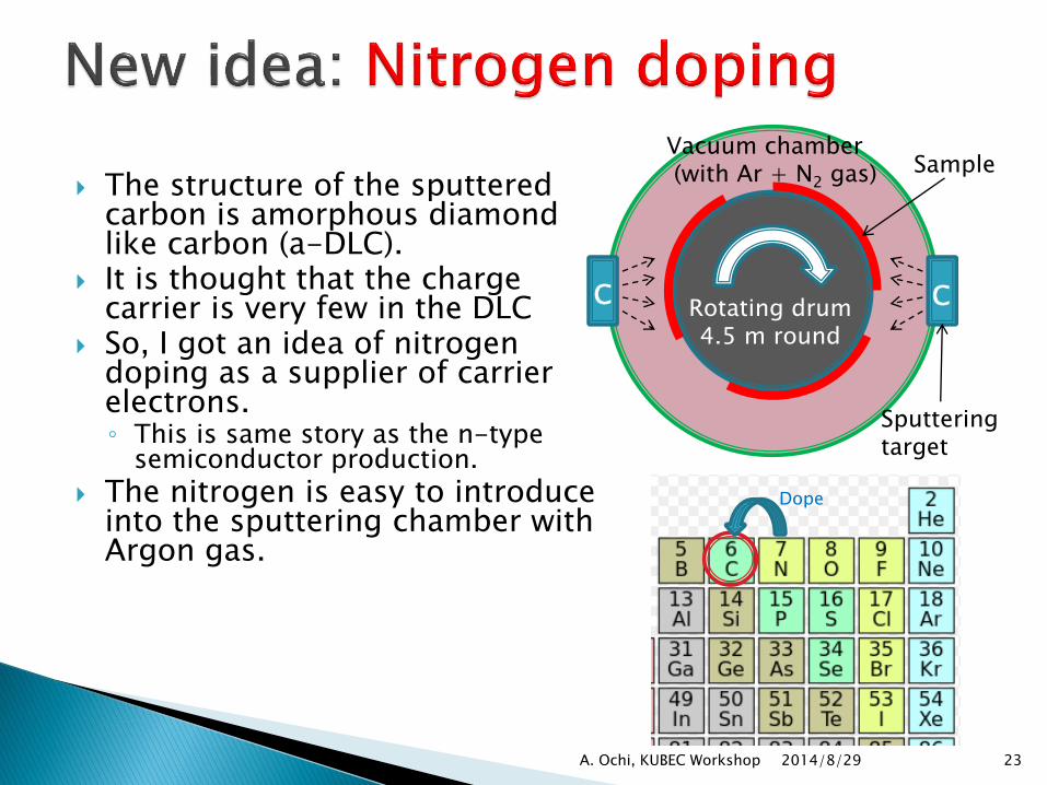
The structure of the sputtered carbon is amorphous diamond like carbon (a-DLC).
It is thought that the charge carrier is very few in the DLC
So, I got an idea of nitrogen doping as a supplier of carrier electrons.◦ This is same story as the n-type
semiconductor production.
The nitrogen is easy to introduce into the sputtering chamber with Argon gas.
2014/8/29A. Ochi, KUBEC Workshop 23
Vacuum chamber(with Ar + N2 gas)
Rotating drum4.5 m round
Sample
Sputteringtarget
C C
Dope
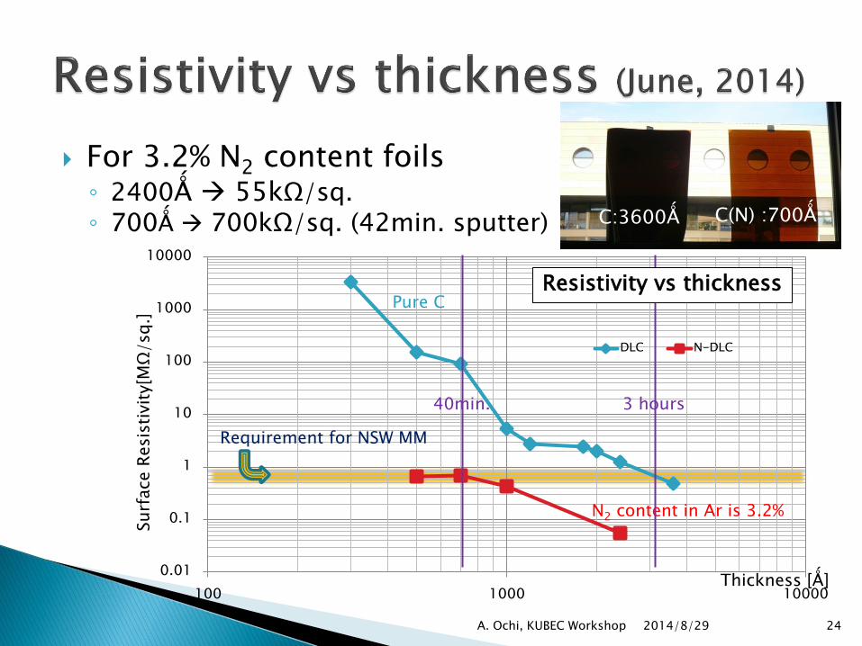
For 3.2% N2 content foils◦ 2400Ǻ 55kΩ/sq.◦ 700Ǻ 700kΩ/sq. (42min. sputter)
2014/8/29A. Ochi, KUBEC Workshop 24
0.01
0.1
1
10
100
1000
10000
100 1000 10000
DLC N-DLC
Surf
ace R
esis
tivit
y[M
Ω/sq.]
Thickness [Ǻ]
N2 content in Ar is 3.2%
Requirement for NSW MM
40min. 3 hours
Resistivity vs thicknessPure C
C:3600Ǻ C(N) :700Ǻ

Resistive μ-PIC◦ New version using carbon sputtering
is being tested
Resistive GEM◦ The resistive electrodes are made by
very thin (50 – 300nm) material It will improve the signal gain
◦ We have just made it, and it is being tested now. (Scienergy + Raytech)
2014/8/29 25A. Ochi, KUBEC Workshop
50 - 100mm
Substrate
Sputteredcarbon
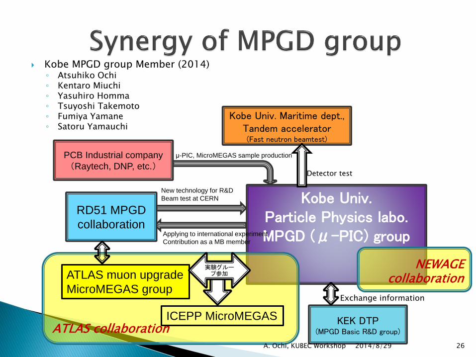
Kobe Univ. Particle Physics labo.MPGD (μ-PIC) group
ATLAS collaboration
Kobe MPGD group Member (2014)◦ Atsuhiko Ochi◦ Kentaro Miuchi◦ Yasuhiro Homma◦ Tsuyoshi Takemoto◦ Fumiya Yamane◦ Satoru Yamauchi
New technology for R&D
Beam test at CERN
Applying to international experiment
Contribution as a MB member
RD51 MPGD
collaboration
KEK DTP(MPGD Basic R&D group)
μ-PIC, MicroMEGAS sample productionPCB Industrial company
(Raytech, DNP, etc.)
ATLAS muon upgrade
MicroMEGAS group
実験グループ参加
ICEPP MicroMEGAS
Exchange information
Kobe Univ. Maritime dept., Tandem accelerator(Fast neutron beamtest)
Detector test
NEWAGE collaboration
2014/8/29 26A. Ochi, KUBEC Workshop
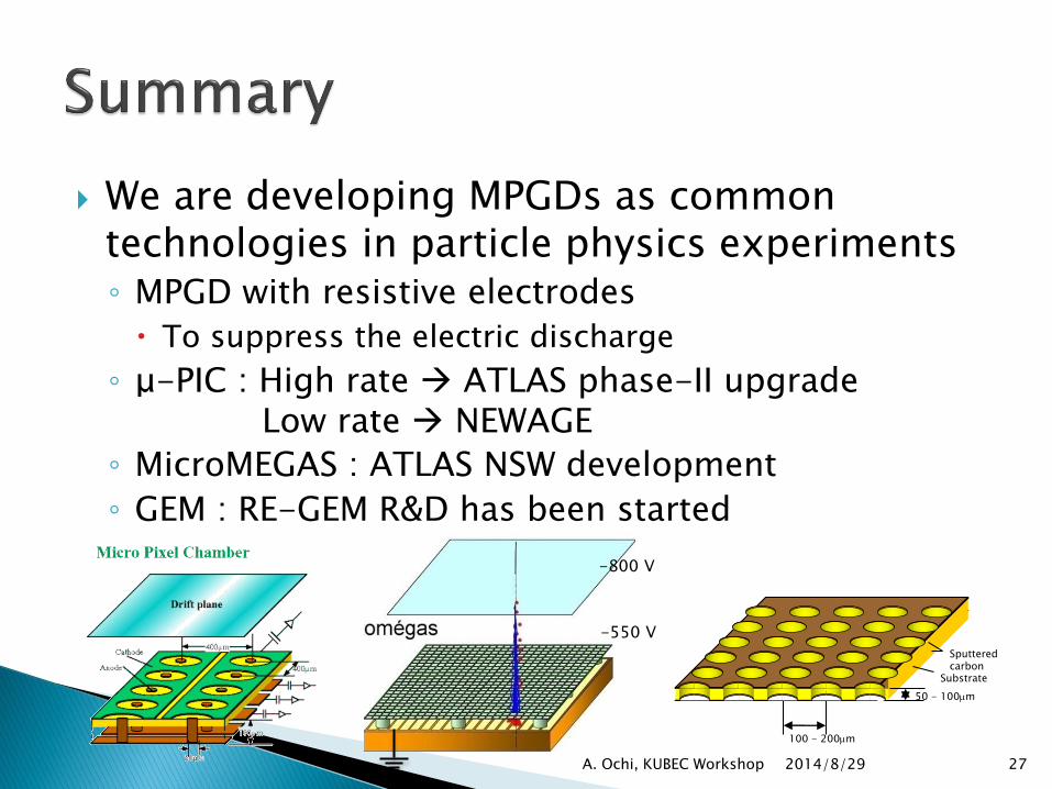
We are developing MPGDs as common technologies in particle physics experiments◦ MPGD with resistive electrodes
To suppress the electric discharge
◦ μ-PIC : High rate ATLAS phase-II upgradeLow rate NEWAGE
◦ MicroMEGAS : ATLAS NSW development
◦ GEM : RE-GEM R&D has been started
2014/8/29A. Ochi, KUBEC Workshop 27
-800 V
-550 V
50 - 100mm
100 - 200mm
Substrate
Sputteredcarbon


![arXiv:1803.11400v1 [hep-ex] 30 Mar 2018 · dKobe University, J-657-8501 Kobe, Japan eAlbert Einstein Center for Fundamental Physics, Laboratory for High Energy Physics (LHEP), University](https://static.fdocument.org/doc/165x107/5b9a048f09d3f29c338d5a8a/arxiv180311400v1-hep-ex-30-mar-2018-dkobe-university-j-657-8501-kobe-japan.jpg)