
J211 MMBFJ211 - N-Channel RF Amplifierakizukidenshi.com/download/ds/fairchild/MMBFJ211.pdf · J211...
9
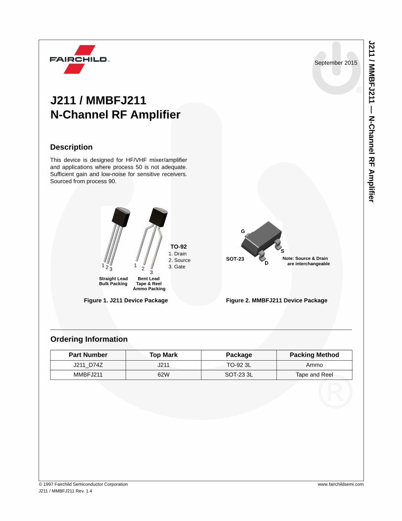
J211 / MMBFJ211 — N-Channel RF Amplifier © 1997 Fairchild Semiconductor Corporation www.fairchildsemi.com J211 / MMBFJ211 Rev. 1.4 September 2015 J211 / MMBFJ211 N-Channel RF Amplifier Ordering Information Figure 1. J211 Device Package Figure 2. MMBFJ211 Device Package Part Number Top Mark Package Packing Method J211_D74Z J211 TO-92 3L Ammo MMBFJ211 62W SOT-23 3L Tape and Reel 1. Drain 1 2 3 1 2 3 Straight Lead Bent Lead TO-92 Bulk Packing Tape & Reel Ammo Packing 2. Source 3. Gate SOT-23 G D S Note: Source & Drain are interchangeable Description This device is designed for HF/VHF mixer/amplifier and applications where process 50 is not adequate. Sufficient gain and low-noise for sensitive receivers. Sourced from process 90.
Transcript of J211 MMBFJ211 - N-Channel RF Amplifierakizukidenshi.com/download/ds/fairchild/MMBFJ211.pdf · J211...
J211 / MM
BF
J211 — N
-Ch
ann
el RF
Am
plifier
© 1997 Fairchild Semiconductor Corporation www.fairchildsemi.com
J211 / MMBFJ211 Rev. 1.4
September 2015
J211 / MMBFJ211N-Channel RF Amplifier
Ordering Information
Figure 1. J211 Device Package Figure 2. MMBFJ211 Device Package
Part Number Top Mark Package Packing Method
J211_D74Z J211 TO-92 3L Ammo
MMBFJ211 62W SOT-23 3L Tape and Reel
1. Drain
1 2 31
23
Straight Lead Bent Lead
TO-92
Bulk Packing Tape & Reel Ammo Packing
2. Source 3. Gate
SOT-23
G
D
SNote: Source & Drain
are interchangeable
Description
This device is designed for HF/VHF mixer/amplifierand applications where process 50 is not adequate.Sufficient gain and low-noise for sensitive receivers.Sourced from process 90.
J211 / MM
BF
J211 — N
-Ch
ann
el RF
Am
plifier
© 1997 Fairchild Semiconductor Corporation www.fairchildsemi.com
J211 / MMBFJ211 Rev. 1.4 2
Absolute Maximum Ratings(1), (2)
Stresses exceeding the absolute maximum ratings may damage the device. The device may not function or be opera-ble above the recommended operating conditions and stressing the parts to these levels is not recommended. In addi-tion, extended exposure to stresses above the recommended operating conditions may affect device reliability. Theabsolute maximum ratings are stress ratings only. Values are at TA = 25°C unless otherwise noted.
Notes:
1. These ratings are based on a maximum junction temperature of 150°C.
2. These are steady-state limits. Fairchild Semiconductor should be consulted on applications involving pulsed or
low-duty-cycle operations.
Thermal CharacteristicsValues are at TA = 25°C unless otherwise noted.
Note:
3. Device mounted on FR-4 PCB 36mm × 18mm × 1.5mm; mounting pad for the collector lead minimum 6cm2.
Electrical CharacteristicsValues are at TA = 25°C unless otherwise noted.
Note:
4. Pulse test: pulse width ≤ 300 μs
Symbol Parameter Value Unit
VDG Drain-Gate Voltage 25 V
VGS Gate-Source Voltage -25 V
IGF Forward Gate Current 10 mA
TJ, TSTG Operating and Storage Junction Temperature Range -55 to 150 °C
Symbol ParameterMax.
UnitJ211(3) MMBFJ211(3)
PDTotal Device Dissipation 350 225 mW
Derate Above 25°C 2.8 1.8 mW/°C
RθJC Thermal Resistance, Junction-to-Case 125 °C/W
RθJA Thermal Resistance, Junction-to-Ambient 357 556 °C/W
Symbol Parameter Conditions Min. Max. Unit
Off Characteristics
V(BR)GSS Gate-Source Breakdown Voltage IG = 1.0 μA, VDS = 0 -25 V
IGSS Gate Reverse Current VGS = 15 V, VDS = 0 -100 pA
VGS(off) Gate-Source Cut-Off Voltage VDS = 15 V, ID = 1.0 nA -2.5 -4.5 V
On Characteristics
IDSS Zero-Gate Voltage Drain Current(4) VDS = 15 V, VGS = 0 7.0 20 mA
Small Signal Characteristics
gfsCommon Source Forward Transconductance
VDS = 15 V, VGS = 0, f = 1.0 kHz
7000 12000 μmhos
gossCommon Source Output Conductance
VDS = 15 V, VGS = 0, f = 1.0 kHz
200 μmhos
J211 / MM
BF
J211 — N
-Ch
ann
el RF
Am
plifier
© 1997 Fairchild Semiconductor Corporation www.fairchildsemi.com
J211 / MMBFJ211 Rev. 1.4 3
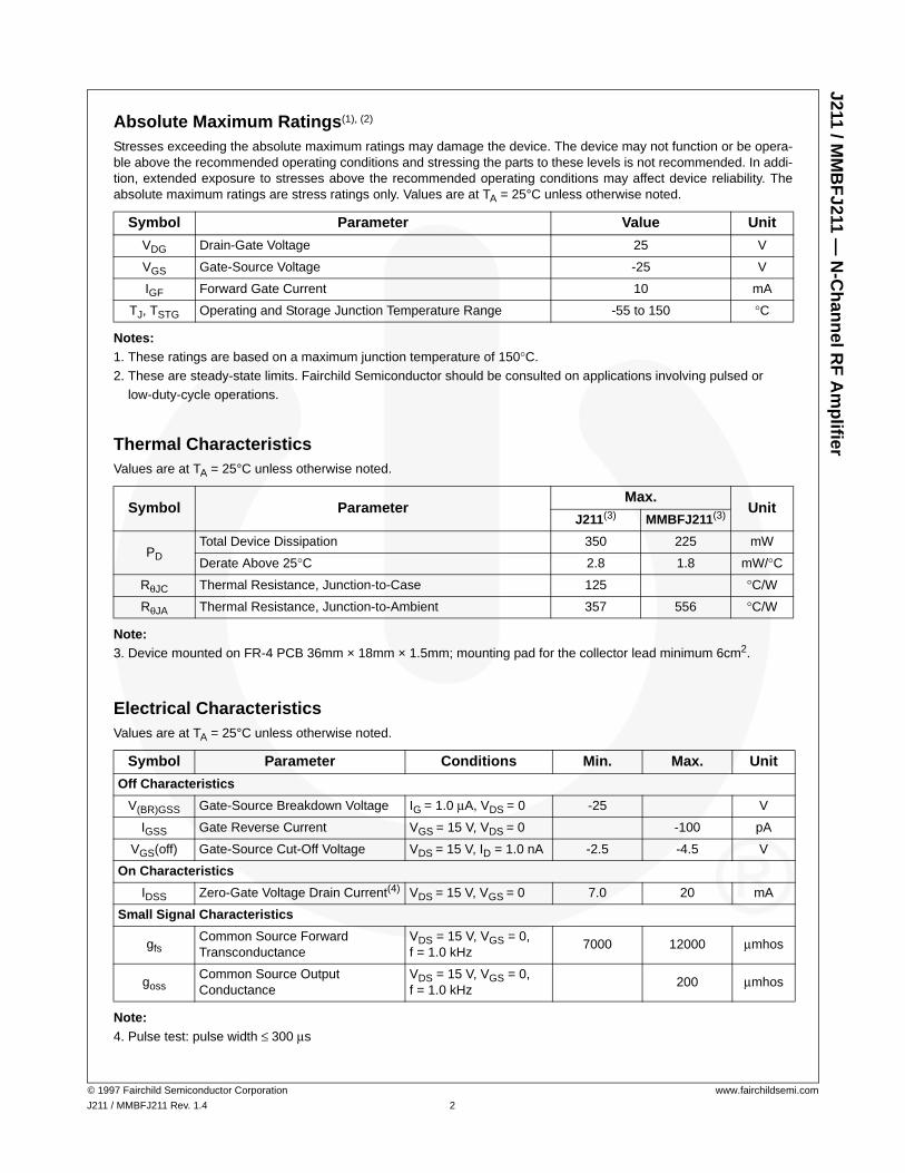
Typical Performance Characteristics
Figure 3. Parameter Interactions Figure 4. Common Drain-Source
Figure 5. Transfer Characteristics Figure 6. Transfer Characteristics
Figure 7. Leakage Current vs. Voltage Figure 8. Noise Voltage vs. Frequency
J211 / MM
BF
J211 — N
-Ch
ann
el RF
Am
plifier
© 1997 Fairchild Semiconductor Corporation www.fairchildsemi.com
J211 / MMBFJ211 Rev. 1.4 4
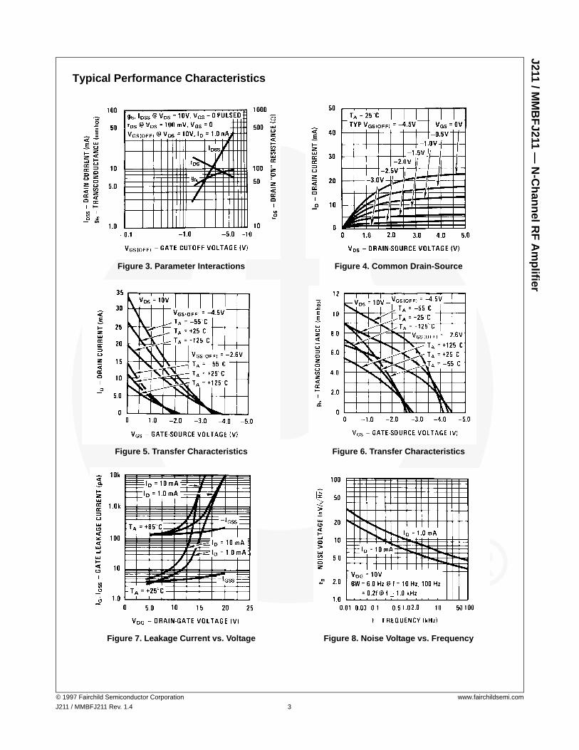
Typical Performance Characteristics (Continued)
Figure 9. Transconductance vs. Drain Current Figure 10. Output Conductance vs. Drain Current
Figure 11. Capacitance vs. Voltage
J211 / MM
BF
J211 — N
-Ch
ann
el RF
Am
plifier
© 1997 Fairchild Semiconductor Corporation www.fairchildsemi.com
J211 / MMBFJ211 Rev. 1.4 5
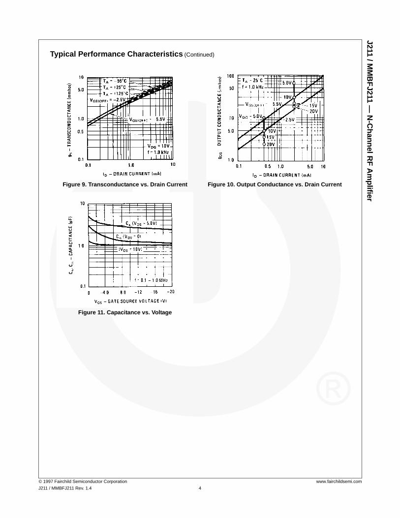
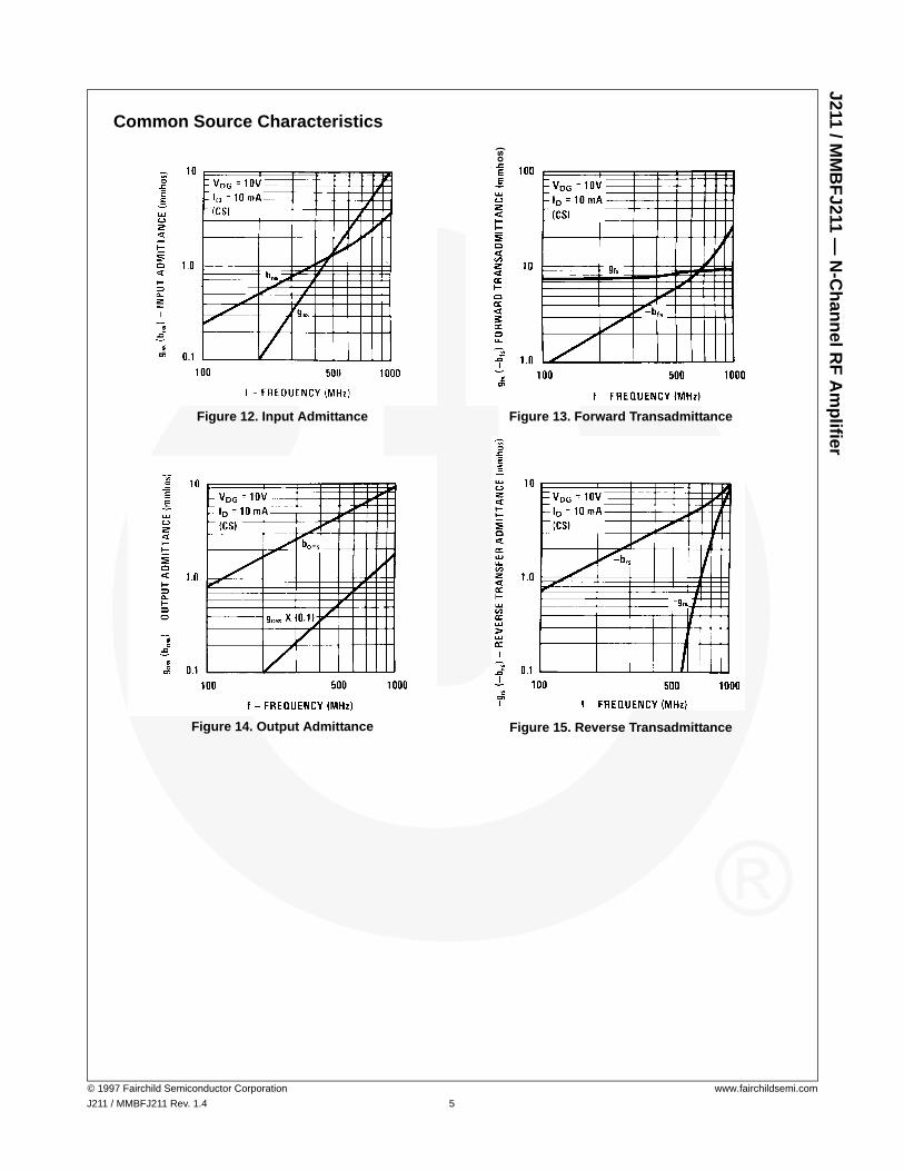
Common Source Characteristics
Figure 12. Input Admittance Figure 13. Forward Transadmittance
Figure 14. Output Admittance Figure 15. Reverse Transadmittance
os)

J211 / MM
BF
J211 — N
-Ch
ann
el RF
Am
plifier
© 1997 Fairchild Semiconductor Corporation www.fairchildsemi.com
J211 / MMBFJ211 Rev. 1.4 6
Common Gate Characteristics
Figure 16. Input Admittance Figure 17. Forward Transadmittance
Figure 18. Output Admittance Figure 19. Reverse Transadmittance
J211 / MM
BF
J211 — N
-Ch
ann
el RF
Am
plifier
© 1997 Fairchild Semiconductor Corporation www.fairchildsemi.com
J211 / MMBFJ211 Rev. 1.4 7
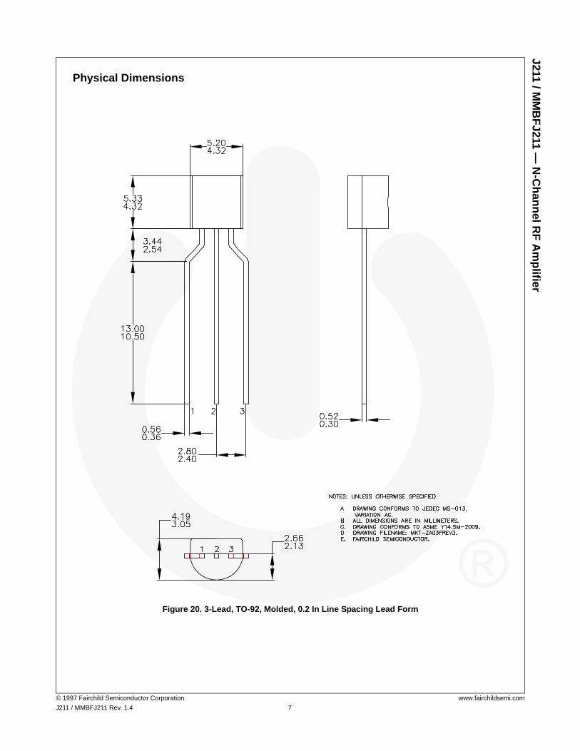
Physical Dimensions
Figure 20. 3-Lead, TO-92, Molded, 0.2 In Line Spacing Lead Form
J211 / MM
BF
J211 — N
-Ch
ann
el RF
Am
plifier
© 1997 Fairchild Semiconductor Corporation www.fairchildsemi.com
J211 / MMBFJ211 Rev. 1.4 8
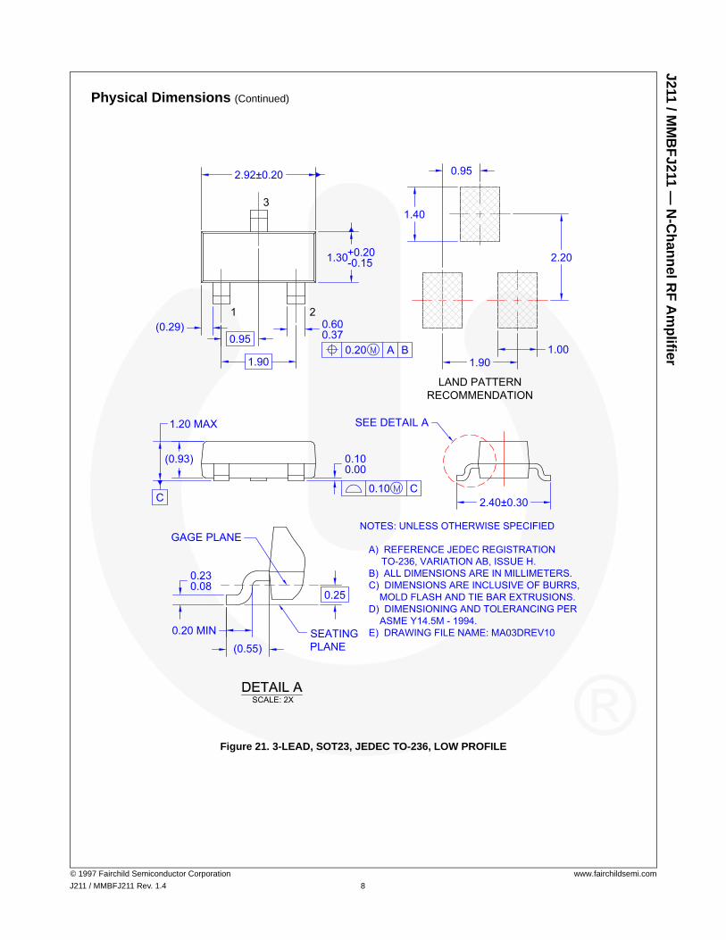
Physical Dimensions (Continued)
Figure 21. 3-LEAD, SOT23, JEDEC TO-236, LOW PROFILE
LAND PATTERN
RECOMMENDATION
NOTES: UNLESS OTHERWISE SPECIFIED
A) REFERENCE JEDEC REGISTRATION
TO-236, VARIATION AB, ISSUE H.
B) ALL DIMENSIONS ARE IN MILLIMETERS.
C) DIMENSIONS ARE INCLUSIVE OF BURRS,
MOLD FLASH AND TIE BAR EXTRUSIONS.
D) DIMENSIONING AND TOLERANCING PER
ASME Y14.5M - 1994.
E) DRAWING FILE NAME: MA03DREV10
3
1 2
SEE DETAIL A
SEATING
PLANE
SCALE: 2X
GAGE PLANE
(0.55)
(0.93)
1.20 MAX
C
0.100.00
0.10 C
2.40±0.30
2.92±0.20
1.30+0.20-0.15
0.600.37
0.20 A B1.90
0.95(0.29)
0.95
1.40
2.20
1.00
1.90
0.25
0.230.08
0.20 MIN
© Fairchild Semiconductor Corporation www.fairchildsemi.com
TRADEMARKS The following includes registered and unregistered trademarks and service marks, owned by Fairchild Semiconductor and/or its global subsidiaries, and is not intended to be an exhaustive list of all such trademarks.
AccuPowerAttitudeEngine™
Awinda®
AX-CAP®*
BitSiC
Build it Now
CorePLUS
CorePOWER
CROSSVOLTCTL
Current Transfer LogicDEUXPEED
®
Dual Cool™ EcoSPARK
®
EfficientMax
ESBC
Fairchild®
Fairchild Semiconductor®
FACT Quiet SeriesFACT
®
FastvCore
FETBench
FPS
F-PFSFRFET
®
Global Power ResourceSM
GreenBridge
Green FPS
Green FPS e-Series
GmaxGTO
IntelliMAX
ISOPLANARMaking Small Speakers Sound Louder
and Better™
MegaBuck
MICROCOUPLER
MicroFET
MicroPak
MicroPak2
MillerDrive
MotionMax
MotionGrid®
MTi®
MTx®
MVN®
mWSaver®
OptoHiTOPTOLOGIC
®
OPTOPLANAR®
®
Power Supply WebDesignerPowerTrench
®
PowerXS™
Programmable Active DroopQFET
®
QS
Quiet Series
RapidConfigure
Saving our world, 1mW/W/kW at a time™
SignalWise
SmartMax
SMART START
Solutions for Your SuccessSPM
®
STEALTHSuperFET
®
SuperSOT -3
SuperSOT -6
SuperSOT -8 SupreMOS
®
SyncFETSync-Lock™
®*
TinyBoost®
TinyBuck®
TinyCalcTinyLogic
®
TINYOPTO
TinyPower
TinyPWM
TinyWire
TranSiC
TriFault DetectTRUECURRENT
®*
SerDes
UHC®
Ultra FRFET
UniFET
VCX
VisualMax
VoltagePlusXS™
Xsens™®
* Trademarks of System General Corporation, used under license by Fairchild Semiconductor.
DISCLAIMER FAIRCHILD SEMICONDUCTOR RESERVES THE RIGHT TO MAKE CHANGES WITHOUT FURTHER NOTICE TO ANY PRODUCTS HEREIN TO IMPROVE RELIABILITY, FUNCTION, OR DESIGN. TO OBTAIN THE LATEST, MOST UP-TO-DATE DATASHEET AND PRODUCT INFORMATION, VISIT OUR WEBSITE AT HTTP://WWW.FAIRCHILDSEMI.COM. FAIRCHILD DOES NOT ASSUME ANY LIABILITY ARISING OUT OF THE APPLICATION OR USE OF ANY PRODUCT OR CIRCUIT DESCRIBED HEREIN; NEITHER DOES IT CONVEY ANY LICENSE UNDER ITS PATENT RIGHTS, NOR THE RIGHTS OF OTHERS. THESE SPECIFICATIONS DO NOT EXPAND THE TERMS OF FAIRCHILD’S WORLDWIDE TERMS AND CONDITIONS, SPECIFICALLY THE WARRANTY THEREIN, WHICH COVERS THESE PRODUCTS.
AUTHORIZED USE Unless otherwise specified in this data sheet, this product is a standard commercial product and is not intended for use in applications that require extraordinary levels of quality and reliability. This product may not be used in the following applications, unless specifically approved in writing by a Fairchild officer: (1) automotive or other transportation, (2) military/aerospace, (3) any safety critical application – including life critical medical equipment – where the failure of the Fairchild product reasonably would be expected to result in personal injury, death or property damage. Customer’s use of this product is subject to agreement of this Authorized Use policy. In the event of an unauthorized use of Fairchild’s product, Fairchild accepts no liability in the event of product failure. In other respects, this product shall be subject to Fairchild’s Worldwide Terms and Conditions of Sale, unless a separate agreement has been signed by both Parties.
ANTI-COUNTERFEITING POLICY Fairchild Semiconductor Corporation's Anti-Counterfeiting Policy. Fairchild's Anti-Counterfeiting Policy is also stated on our external website, www.fairchildsemi.com, under Terms of Use
Counterfeiting of semiconductor parts is a growing problem in the industry. All manufacturers of semiconductor products are experiencing counterfeiting of their parts. Customers who inadvertently purchase counterfeit parts experience many problems such as loss of brand reputation, substandard performance, failed applications, and increased cost of production and manufacturing delays. Fairchild is taking strong measures to protect ourselves and our customers from the proliferation of counterfeit parts. Fairchild strongly encourages customers to purchase Fairchild parts either directly from Fairchild or from Authorized Fairchild Distributors who are listed by country on our web page cited above. Products customers buy either from Fairchild directly or from Authorized Fairchild Distributors are genuine parts, have full traceability, meet Fairchild's quality standards for handling and storage and provide access to Fairchild's full range of up-to-date technical and product information. Fairchild and our Authorized Distributors will stand behind all warranties and will appropriately address any warranty issues that may arise. Fairchild will not provide any warranty coverage or other assistance for parts bought from Unauthorized Sources. Fairchild is committed to combat this global problem and encourage our customers to do their part in stopping this practice by buying direct or from authorized distributors.
PRODUCT STATUS DEFINITIONS Definition of Terms Datasheet Identification Product Status Definition
Advance Information Formative / In Design Datasheet contains the design specifications for product development. Specifications may change in any manner without notice.
Preliminary First Production Datasheet contains preliminary data; supplementary data will be published at a later date. Fairchild Semiconductor reserves the right to make changes at any time without notice to improve design.
No Identification Needed Full Production Datasheet contains final specifications. Fairchild Semiconductor reserves the right to make changes at any time without notice to improve the design.
Obsolete Not In Production Datasheet contains specifications on a product that is discontinued by Fairchild Semiconductor. The datasheet is for reference information only.
Rev. I77
®


![Atmel AT02865: RF Layout with Microstripww1.microchip.com/downloads/en/AppNotes/Atmel-42131-RF... · 2017-01-05 · Atmel AT02865: RF Layout with Microstrip [APPLICATION NOTE] 42131B−WIRELESS−05/2013](https://static.fdocument.org/doc/165x107/5e2528a335871412bd6f1bd7/atmel-at02865-rf-layout-with-2017-01-05-atmel-at02865-rf-layout-with-microstrip.jpg)