
IV - Synchronization · e–ciency by allocating a certain fraction of the transmitted power to the...
23
IV - Synchronization * 1 Introduction Coherent (or synchronous) detection of digitally modulated signals using a receiver as the ML receiver of Fig. 2, chapter 3, requires two types of synchronization: a) carrier (or phase) synchronization: the generation of reference signals ψ 0 (t), ψ 1 (t),...,ψ N -1 (t) requires the knowledge of the carrier frequency and phase. b) symbol synchronization: integration and sampling of the integrators outputs require the knowledge of the starting and finishing times of each symbol (symbol clock). Carrier synchronization is usually obtained from the modulated signal (affected by noise) through a feedback circuit based on the phase locked-loop (PLL). Obviously, in a noncoherent system, carrier synchronization is of no concern. Synchronization can be implemented in one of two fundamentally different ways [4]: • Data-aided synchronization In data-aided synchronization systems, a preamble is transmitted along with the data-bearing signal in a time-multiplexed manner on a periodic basis. The pream- ble contains information about the carrier and symbol timing, which is extracted by appropriate processing of the channel output at the receiver. Such an approach is com- monly used in digital satellite and wireless communications, where the motivation is to minimize the time required to synchronize the receiver to the transmitter. Its limita- tions are two-fold: (1) reduced data-throughput efficiency that results from assigning a certain portion of each transmitted frame to the preamble; and (2) reduced power efficiency by allocating a certain fraction of the transmitted power to the transmission of the preamble. • Nondata-aided synchronization In this approach, the use of a preamble is avoided, and the receiver has the task of establishing synchronization by extracting the necessary information from the modu- * FDNunes, IST 2013. 76
-
Upload
vuongquynh -
Category
Documents
-
view
217 -
download
3
Transcript of IV - Synchronization · e–ciency by allocating a certain fraction of the transmitted power to the...
IV - Synchronization∗
1 Introduction
Coherent (or synchronous) detection of digitally modulated signals using a receiver as
the ML receiver of Fig. 2, chapter 3, requires two types of synchronization:
a) carrier (or phase) synchronization: the generation of reference signals ψ0(t),
ψ1(t), . . . , ψN−1(t) requires the knowledge of the carrier frequency and phase.
b) symbol synchronization: integration and sampling of the integrators outputs
require the knowledge of the starting and finishing times of each symbol (symbol clock).
Carrier synchronization is usually obtained from the modulated signal (affected by
noise) through a feedback circuit based on the phase locked-loop (PLL). Obviously, in
a noncoherent system, carrier synchronization is of no concern.
Synchronization can be implemented in one of two fundamentally different ways
[4]:
• Data-aided synchronization
In data-aided synchronization systems, a preamble is transmitted along with the
data-bearing signal in a time-multiplexed manner on a periodic basis. The pream-
ble contains information about the carrier and symbol timing, which is extracted by
appropriate processing of the channel output at the receiver. Such an approach is com-
monly used in digital satellite and wireless communications, where the motivation is to
minimize the time required to synchronize the receiver to the transmitter. Its limita-
tions are two-fold: (1) reduced data-throughput efficiency that results from assigning
a certain portion of each transmitted frame to the preamble; and (2) reduced power
efficiency by allocating a certain fraction of the transmitted power to the transmission
of the preamble.
• Nondata-aided synchronization
In this approach, the use of a preamble is avoided, and the receiver has the task of
establishing synchronization by extracting the necessary information from the modu-
∗FDNunes, IST 2013.
76
2 PHASE-LOCKED LOOP (PLL) 77
lated signal. Both throughput and power efficiency are thereby improved but at the
expense of an increase in the time taken to establish synchronization.
In this chapter we consider only nondata-aided synchronization schemes where we
may identify two approaches for solving the synchronization problem: the classical ap-
proach based on the phase-locked loop (PLL), and the algorithmic (modern) approach
that resorts to the maximum likelihood (ML) estimation.
2 phase-locked loop (PLL)
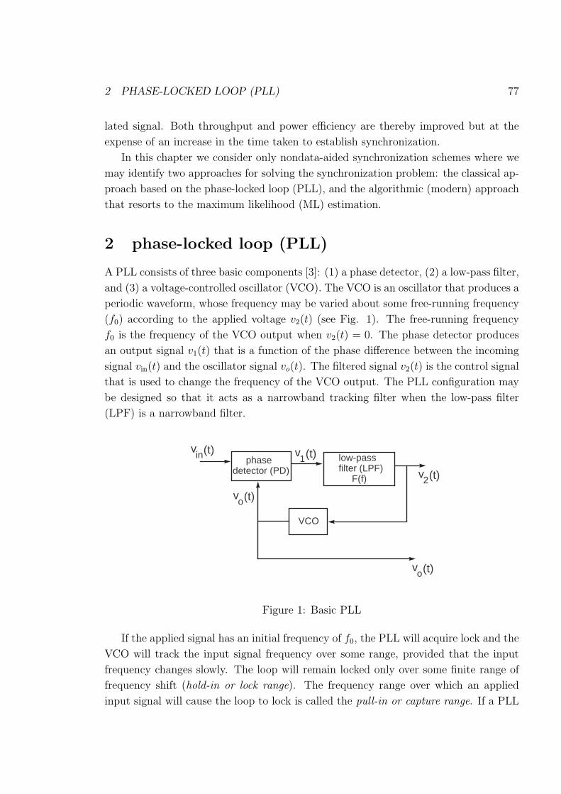
A PLL consists of three basic components [3]: (1) a phase detector, (2) a low-pass filter,
and (3) a voltage-controlled oscillator (VCO). The VCO is an oscillator that produces a
periodic waveform, whose frequency may be varied about some free-running frequency
(f0) according to the applied voltage v2(t) (see Fig. 1). The free-running frequency
f0 is the frequency of the VCO output when v2(t) = 0. The phase detector produces
an output signal v1(t) that is a function of the phase difference between the incoming
signal vin(t) and the oscillator signal vo(t). The filtered signal v2(t) is the control signal
that is used to change the frequency of the VCO output. The PLL configuration may
be designed so that it acts as a narrowband tracking filter when the low-pass filter
(LPF) is a narrowband filter.
phasedetector (PD)
low-pass filter (LPF) F(f)
VCO
vo(t)
vo(t)
vin(t) v
1(t)
v2(t)
Figure 1: Basic PLL
If the applied signal has an initial frequency of f0, the PLL will acquire lock and the
VCO will track the input signal frequency over some range, provided that the input
frequency changes slowly. The loop will remain locked only over some finite range of
frequency shift (hold-in or lock range). The frequency range over which an applied
input signal will cause the loop to lock is called the pull-in or capture range. If a PLL
2 PHASE-LOCKED LOOP (PLL) 78
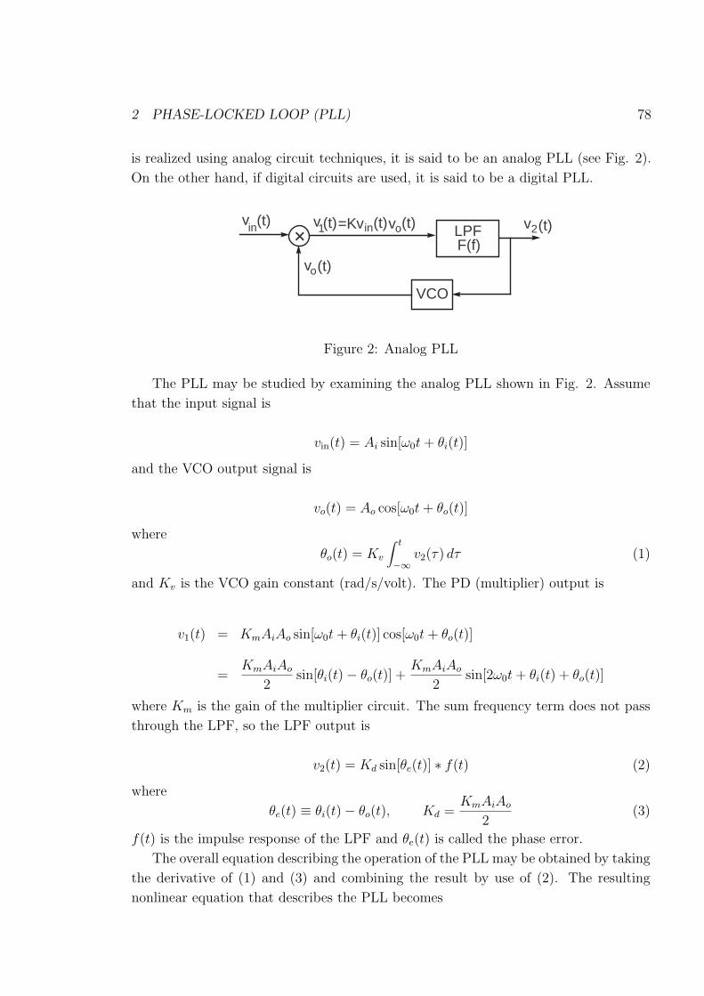
is realized using analog circuit techniques, it is said to be an analog PLL (see Fig. 2).
On the other hand, if digital circuits are used, it is said to be a digital PLL.
+ LPFF(f)
VCO
vin(t)
vo(t)
v1(t)=Kvin(t)vo(t) v2(t)
Figure 2: Analog PLL
The PLL may be studied by examining the analog PLL shown in Fig. 2. Assume
that the input signal is
vin(t) = Ai sin[ω0t + θi(t)]
and the VCO output signal is
vo(t) = Ao cos[ω0t + θo(t)]
where
θo(t) = Kv
∫ t
−∞v2(τ) dτ (1)
and Kv is the VCO gain constant (rad/s/volt). The PD (multiplier) output is
v1(t) = KmAiAo sin[ω0t + θi(t)] cos[ω0t + θo(t)]
=KmAiAo
2sin[θi(t)− θo(t)] +
KmAiAo
2sin[2ω0t + θi(t) + θo(t)]
where Km is the gain of the multiplier circuit. The sum frequency term does not pass
through the LPF, so the LPF output is
v2(t) = Kd sin[θe(t)] ∗ f(t) (2)
where
θe(t) ≡ θi(t)− θo(t), Kd =KmAiAo
2(3)
f(t) is the impulse response of the LPF and θe(t) is called the phase error.
The overall equation describing the operation of the PLL may be obtained by taking
the derivative of (1) and (3) and combining the result by use of (2). The resulting
nonlinear equation that describes the PLL becomes
2 PHASE-LOCKED LOOP (PLL) 79
dθe(t)
dt=
dθi(t)
dt−KdKv
∫ ∞
−∞sin[θe(λ)]f(t− λ) dλ
where θe(t) is the unknown and θi(t) is the forcing function.
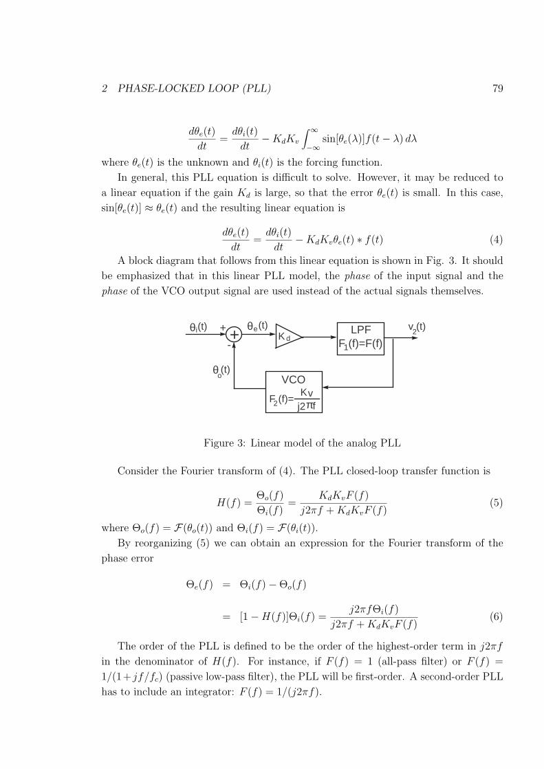
In general, this PLL equation is difficult to solve. However, it may be reduced to
a linear equation if the gain Kd is large, so that the error θe(t) is small. In this case,
sin[θe(t)] ≈ θe(t) and the resulting linear equation is
dθe(t)
dt=
dθi(t)
dt−KdKvθe(t) ∗ f(t) (4)
A block diagram that follows from this linear equation is shown in Fig. 3. It should
be emphasized that in this linear PLL model, the phase of the input signal and the
phase of the VCO output signal are used instead of the actual signals themselves.
+ LPFF (f)=F(f)1
VCO
F (f)=Kv
j2πf2
θ
θ
+
-
θi
o
e(t) (t)
(t)
K d
v (t)2
Figure 3: Linear model of the analog PLL
Consider the Fourier transform of (4). The PLL closed-loop transfer function is
H(f) =Θo(f)
Θi(f)=
KdKvF (f)
j2πf + KdKvF (f)(5)
where Θo(f) = F(θo(t)) and Θi(f) = F(θi(t)).
By reorganizing (5) we can obtain an expression for the Fourier transform of the
phase error
Θe(f) = Θi(f)−Θo(f)
= [1−H(f)]Θi(f) =j2πfΘi(f)
j2πf + KdKvF (f)(6)
The order of the PLL is defined to be the order of the highest-order term in j2πf
in the denominator of H(f). For instance, if F (f) = 1 (all-pass filter) or F (f) =
1/(1+ jf/fc) (passive low-pass filter), the PLL will be first-order. A second-order PLL
has to include an integrator: F (f) = 1/(j2πf).
2 PHASE-LOCKED LOOP (PLL) 80
Equation (6) can be used in conjunction with the final value theorem of Fourier
transform to determine the steady-state error response of a loop to a variety of possible
input characteristics. The steady-state error is the residual error after all transients
have died away, and thus provide a measure of a loop’s ability to cope with various
types of changes in the input. The final value theorem states that [6]
limt→∞ θe(t) = lim
f→0j2πfΘe(f) (7)
Combining equations (6) and (7) yields
limt→∞ θe(t) = lim
f→0
(j2πf)2Θi(f)
j2πf + KdKvF (f)(8)
Let us analyze the PLL response to a (1) phase step and a (2) frequency step.
Assuming that the PLL was originally in phase lock, a phase step will throw the
loop of of lock. Having abruptly changed, however, the input phase again becomes
stable. The Fourier transform of a phase step is
Θi(f) = F{∆φu(t)} =∆φ
j2πf(9)
where ∆φ is the magnitude of the step in radians and u(t) is the unit step function.
Replacing (9) in (8) leads to
limt→∞ θe(t) = lim
f→0
j2πf∆φ
j2πf + KdKvF (f)= 0
assuming that F (0) 6= 0. Thus, a first-order PLL will automatically tend to recover
phase lock if the input is displaced by a constant phase. This is clearly a very desirable
loop characteristic.
Next, consider the PLL steady-state response to a frequency step at the input. A
frequency step (or phase ramp) can approximate the effect of a frequency Doppler shift
in the incoming signal due to the relative motion between the transmitter and the
receiver.The Fourier transform of the phase characteristic will be the transform of the
integral of the frequency characteristic. Thus
Θi(f) =∆ω
(j2πf)2(10)
where ∆ω is the magnitude of the frequency step in rad/s. Replacing (10) in (8) gives
limt→∞ θe(t) = lim
f→0
∆ω
j2πf + KdKvF (f)=
∆ω
KdKvF (0)(11)
Equation (11) indicates that the loop will track the input phase ramp with a con-
stant steady-state error whose value will depend on the gain term, KdKv, and the
3 MAXIMUM LIKELIHOOD ESTIMATION OF PARAMETERS 81
magnitude of the frequency step. One way to achieve a null error in (11) is that the
denominator of F (f) contains j2πf as a factor which is equivalent to having a perfect
integrator in the loop filter (second-order PLL). It is not possible to build a perfect
integrator, but one may be closely approximated either digitally or by using active
integrated circuits. It should be noted that even with a nonzero Doppler velocity, the
frequency is still being tracked. There are applications where tracking a zero phase
error is not important provided that frequency is tracked. Noncoherent signaling, such
as M-FSK modulation is an example [6].
The steady-state analysis above assumed that the input signal was noise free, which
is not true in practical transmission systems. If the noise process is white with power
spectral density Gw(f) = N0/2 and the small-angle approximation holds (that is, if
the loop is successfully tracking the input phase), the output phase variance is given
by [2], [10]
σ2e =
2N0BL
A2i
rad2 (12)
where
BL =1
|H(0)|2∫ ∞
0|H(f)|2 df Hz
is the single-sided equivalent noise bandwidth.
In order to tabulate the noise bandwidth for various cases, define the closed-loop
transfer function H(s) of a n-th order PLL by
H(s) =C0 + C1s + C2s
2 + . . . + Cn−1sn−1
d0 + d1s + d2s2 + . . . + dnsn
The loop noise bandwidths are [10]
n = 1 : BL =C2
0
4d0d1
n = 2 : BL =C2
0d2 + C21d0
4d0d1d2
The phase variance σ2e is a measure of the amount of jitter in the VCO output due
to noise at the input. Equations (6) and (12) highlight one of the many trade-offs
in communication theory. Clearly, one would wish σ2e to be small, which implies a
small loop bandwidth, BL, that requires a narrow H(f). However, it can be inferred
from (6) that the narrower the effective bandwidth of H(f) is, the poorer will be the
loop’s ability to track incoming signal phase changes, Θi(f). Thus, a loop design must
balance noise response with desired input phase response [6].
3 Maximum likelihood estimation of parameters
Consider the received complex signal
3 MAXIMUM LIKELIHOOD ESTIMATION OF PARAMETERS 82
v(t) = c(t, γ) + n(t), −T0/2 ≤ t ≤ T0/2
where γ is an unknown vector parameter to be estimated and n(t) is complex white
Gaussian noise. Consider the Fourier series expansions of v(t) and c(t, γ) restricted to
the interval [−T0/2, T0/2], according to
v(t) =∞∑
i=−∞vi exp(j2πif0t), f0 = 1/T0
c(t, γ) =∞∑
i=−∞ci exp(j2πif0t)
where the Fourier coeffients of v(t) on the interval [−T0/2, T0/2] are
vi =1
T0
∫ T0/2
−T0/2v(t) exp(−j2πif0t) dt = ci + ni
and
ci =1
T0
∫ T0/2
−T0/2c(t, γ) exp(−j2πif0t) dt
ni =1
T0
∫ T0/2
−T0/2n(t) exp(−j2πif0t) dt
Thus, the coefficients {. . . , v−1, v0, v1, . . .} are a set of Gaussian random variables.
Because the noise n(t) is white, the complex random variables vi are independent, with
means ci and equal variances σ2. The probability density function is [9]
p(v−k, . . . , vk|c(t, γ)) =1
(πσ2)2k+1exp
− 1
σ2
k∑
i=−k
|vi − ci|2
From the receiver point of view, {v−k, . . . , vk} is a set of observations (known quan-
tities) and p(v−k, . . . , vk|c(t, γ)) is a function of the unknown vector parameter γ. This
probability density function is known as a likelihood function. The logarithmic form of
the likelihood function (log-likelihood function) is
Λ(γ) = log p(v−k, . . . , vk|c(t, γ))
This function is preferred because it replaces products of likelihood functions by
sums of log-likelihoods. Thus
Λ(γ) = C − 1
σ2
k∑
i=−k
|vi − ci|2
3 MAXIMUM LIKELIHOOD ESTIMATION OF PARAMETERS 83
where C does not depend on γ. Now let k → ∞ and use the Parseval’s theorem for
the Fourier series
1
T0
∫ T0/2
−T0/2|v(t)|2 dt =
∞∑
i=−∞|vi|2
it yields
limk→∞
Λ(γ) = C − 1
T0σ2
∫ T0/2
−T0/2|v(t)− c(t, γ)|2 dt
The maximum likelihood estimate of the parameter vector γ is the one that max-
imizes Λ(γ). Thus, constants C and T0σ2 are irrelevant and can be omitted. The
maximum likelihood estimate of parameter vector γ is the one that maximizes [7]
Λ(γ) = −∫ T0/2
−T0/2|v(t)− c(t, γ)|2 dt
3.1 ML estimation of the phase
Suppose now that the received signal at complex baseband is
v(t) = s(t)ejθ + nR(t) + jnI(t)
where θ is the phase to be estimated, nR(t) and nI(t) are independent, Gaussian, white
noise processes and s(t) is a finite energy pulse, possibly complex. The log-likelihood
statistic is
Λ(θ) = −∫ ∞
−∞|v(t)− s(t)ejθ|2 dt
= −∫ ∞
−∞[v2
R(t) + v2I (t) + s2
R(t) + s2I(t)] dt
+ cos θ∫ ∞
−∞[2vR(t)sR(t) + 2vI(t)sI(t)] dt
− sin θ∫ ∞
−∞[2vR(t)sI(t)− 2VI(t)sR(t)] dt
Now, doing
∂Λ(θ)
∂θ= 0
leads to the maximum likelihood estimate of the phase [7]
3 MAXIMUM LIKELIHOOD ESTIMATION OF PARAMETERS 84
θ̂ML = arctan
∫∞−∞[vI(t)sR(t)− vR(t)sI(t)] dt∫∞−∞[vR(t)sR(t) + vI(t)sI(t)] dt
(13)
3.2 ML estimation of the delay
Suppose that a received signal at complex baseband is
v(t) = s(t− α) + nR(t) + jnI(t)
where α is the delay parameter to be estimated, nR(t) and nI(t) are independent,
Gaussian, identically distributed, white noise processes and s(t) is a differentiable finite
energy pulse, possibly complex. The log-likelihood function is
Λ(α) = −∫ ∞
−∞|v(λ)− s(λ− α)|2 dλ
= −Ev − Es + 2∫ ∞
−∞vR(t)sR(λ− α) + vI(t)sI(λ− α) dλ
Doing now
∂Λ(α)
∂α= 0
leads to the maximum likelihood estimate of the delay [7]
Re
[∫ ∞
−∞ds(λ− α)
dαv∗(λ) dλ
]= 0 (14)
Let u = λ− α. We obtain for the integral in (14)
∫ ∞
−∞ds(λ− α)
dαv∗(λ) dλ =
∫ ∞
−∞ds(u)
du
du
dαv∗(u + α)
dλ
dudu
= −∫ ∞
−∞ds(u)
duv∗(u + α) du
Consider now t = u + α. We obtain
−∫ ∞
−∞ds(u)
duv∗(u + α) du = −
∫ ∞
−∞ds(t− α)
dtv∗(t) dt
which leads finally to
Re
[∫ ∞
−∞ds(t− α)
dtv∗(t) dt
]= 0 (15)
4 CARRIER SYNCHRONIZATION 85
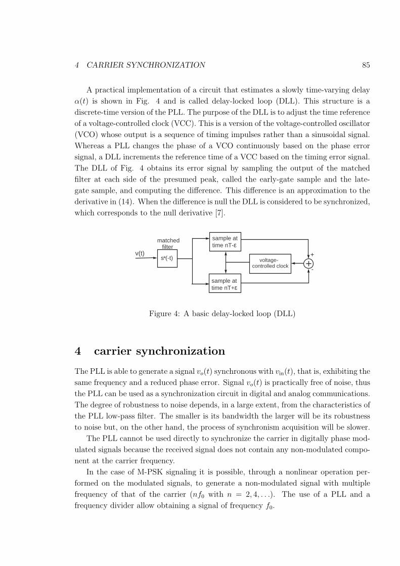
A practical implementation of a circuit that estimates a slowly time-varying delay
α(t) is shown in Fig. 4 and is called delay-locked loop (DLL). This structure is a
discrete-time version of the PLL. The purpose of the DLL is to adjust the time reference
of a voltage-controlled clock (VCC). This is a version of the voltage-controlled oscillator
(VCO) whose output is a sequence of timing impulses rather than a sinusoidal signal.
Whereas a PLL changes the phase of a VCO continuously based on the phase error
signal, a DLL increments the reference time of a VCC based on the timing error signal.
The DLL of Fig. 4 obtains its error signal by sampling the output of the matched
filter at each side of the presumed peak, called the early-gate sample and the late-
gate sample, and computing the difference. This difference is an approximation to the
derivative in (14). When the difference is null the DLL is considered to be synchronized,
which corresponds to the null derivative [7].
sample at time nT-ε
sample at time nT+ε
voltage-controlled clock +
+
-
matched filter
s (-t)*v(t)
Figure 4: A basic delay-locked loop (DLL)
4 carrier synchronization
The PLL is able to generate a signal vo(t) synchronous with vin(t), that is, exhibiting the
same frequency and a reduced phase error. Signal vo(t) is practically free of noise, thus
the PLL can be used as a synchronization circuit in digital and analog communications.
The degree of robustness to noise depends, in a large extent, from the characteristics of
the PLL low-pass filter. The smaller is its bandwidth the larger will be its robustness
to noise but, on the other hand, the process of synchronism acquisition will be slower.
The PLL cannot be used directly to synchronize the carrier in digitally phase mod-
ulated signals because the received signal does not contain any non-modulated compo-
nent at the carrier frequency.
In the case of M-PSK signaling it is possible, through a nonlinear operation per-
formed on the modulated signals, to generate a non-modulated signal with multiple
frequency of that of the carrier (nf0 with n = 2, 4, . . .). The use of a PLL and a
frequency divider allow obtaining a signal of frequency f0.
4 CARRIER SYNCHRONIZATION 86
Let
si(t) = A cos(ω0t +
2πi
M
), 0 ≤ t ≤ Ts, i = 0, 1, . . . , M − 1
be the M-PSK modulated signal. Taking into account that
cosM x =1
2M
2
M/2−1∑
k=0
(M
k
)cos[(M − 2k)x] +
(M
M/2
)
yields
sMi (t) =
(A
2
)M2
M/2−1∑
k=0
(M
k
)cos
[(M − 2k)
(ω0t +
2πi
M
)]+
(M
M/2
)
Therefore, the component at frequency Mf0 (corresponding to k = 0) is free from
digital modulation, that is, it does not depend on the phase 2πi/M of the modulated
signal.
Let us consider, for example, the binary PSK modulation. The received signals are
given by
r(t) = ±A cos(ω0t) + n(t),
where n(t) is channel noise. One solution to eliminate the digital modulation consists
of squaring the signal according to
r2(t) = A2cos2(ω0t)︸ ︷︷ ︸x(t)
+ n2(t)± 2An(t) cos(ω0t)︸ ︷︷ ︸z(t)
,
where
x(t) =A2
2[1 + cos(2ω0t)]
is free from modulation and can used for synchronization purposes. This is carried out
by a PLL with central frequency 2f0 followed by a frequency divider by 2. The signal
component z(t) of r2(t) is noise, behaving as a disturbance to the PLL operation. This
synchronization circuit is called a squaring loop.
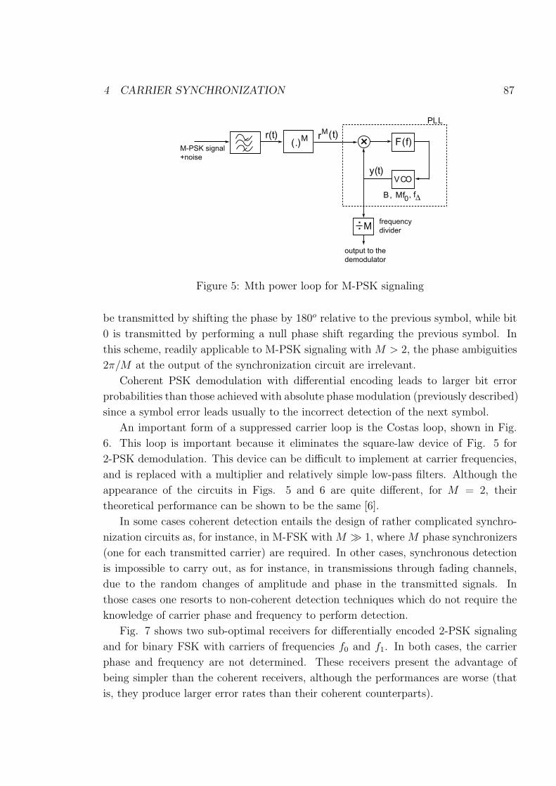
We show in Fig. 5 a possible synchronization scheme for the M-PSK signaling (Mth
power loop).
The frequency divider by M introduces a phase ambiguity of 2π/M at the output
of the synchronization circuit. In fact, we can obtain one of the signals cos(ω0t +
2kπ/M), k = 0, 1, . . . , M−1. This drawback is usually solved using differential encoding
of the M-PSK signal.
In differential encoding the information is carried in the phase shifts relative the
the phase of the previously transmitted symbol. For instance, in binary PSK bit 1 may
4 CARRIER SYNCHRONIZATION 87
(.) M
+ F(f)
:
VCO
M
y(t)
0 , f ∆
PLL
r(t) r M (t)
B, Mf
M-PSK signal
+noise
output to the
demodulator
frequency
divider
Figure 5: Mth power loop for M-PSK signaling
be transmitted by shifting the phase by 180o relative to the previous symbol, while bit
0 is transmitted by performing a null phase shift regarding the previous symbol. In
this scheme, readily applicable to M-PSK signaling with M > 2, the phase ambiguities
2π/M at the output of the synchronization circuit are irrelevant.
Coherent PSK demodulation with differential encoding leads to larger bit error
probabilities than those achieved with absolute phase modulation (previously described)
since a symbol error leads usually to the incorrect detection of the next symbol.
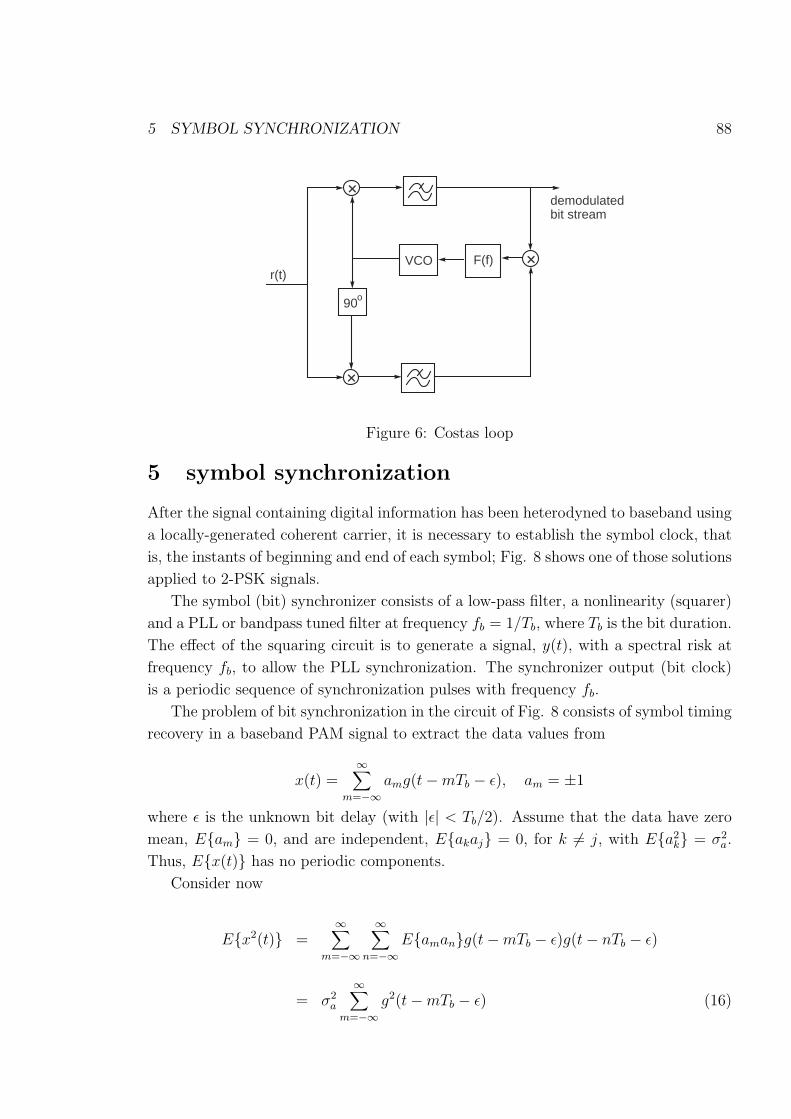
An important form of a suppressed carrier loop is the Costas loop, shown in Fig.
6. This loop is important because it eliminates the square-law device of Fig. 5 for
2-PSK demodulation. This device can be difficult to implement at carrier frequencies,
and is replaced with a multiplier and relatively simple low-pass filters. Although the
appearance of the circuits in Figs. 5 and 6 are quite different, for M = 2, their
theoretical performance can be shown to be the same [6].
In some cases coherent detection entails the design of rather complicated synchro-
nization circuits as, for instance, in M-FSK with M À 1, where M phase synchronizers
(one for each transmitted carrier) are required. In other cases, synchronous detection
is impossible to carry out, as for instance, in transmissions through fading channels,
due to the random changes of amplitude and phase in the transmitted signals. In
those cases one resorts to non-coherent detection techniques which do not require the
knowledge of carrier phase and frequency to perform detection.
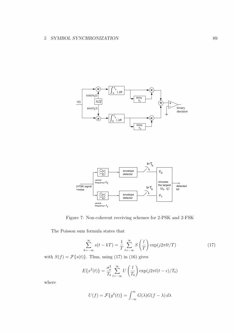
Fig. 7 shows two sub-optimal receivers for differentially encoded 2-PSK signaling
and for binary FSK with carriers of frequencies f0 and f1. In both cases, the carrier
phase and frequency are not determined. These receivers present the advantage of
being simpler than the coherent receivers, although the performances are worse (that
is, they produce larger error rates than their coherent counterparts).
5 SYMBOL SYNCHRONIZATION 88
+
+
90o
VCO F(f) +
demodulatedbit stream
r(t)
Figure 6: Costas loop
5 symbol synchronization
After the signal containing digital information has been heterodyned to baseband using
a locally-generated coherent carrier, it is necessary to establish the symbol clock, that
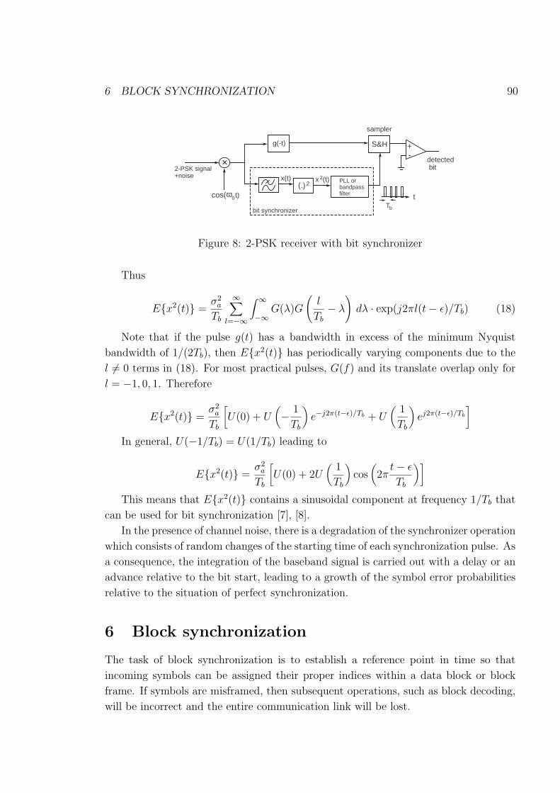
is, the instants of beginning and end of each symbol; Fig. 8 shows one of those solutions
applied to 2-PSK signals.
The symbol (bit) synchronizer consists of a low-pass filter, a nonlinearity (squarer)
and a PLL or bandpass tuned filter at frequency fb = 1/Tb, where Tb is the bit duration.
The effect of the squaring circuit is to generate a signal, y(t), with a spectral risk at
frequency fb, to allow the PLL synchronization. The synchronizer output (bit clock)
is a periodic sequence of synchronization pulses with frequency fb.
The problem of bit synchronization in the circuit of Fig. 8 consists of symbol timing
recovery in a baseband PAM signal to extract the data values from
x(t) =∞∑
m=−∞amg(t−mTb − ε), am = ±1
where ε is the unknown bit delay (with |ε| < Tb/2). Assume that the data have zero
mean, E{am} = 0, and are independent, E{akaj} = 0, for k 6= j, with E{a2k} = σ2
a.
Thus, E{x(t)} has no periodic components.
Consider now
E{x2(t)} =∞∑
m=−∞
∞∑
n=−∞E{aman}g(t−mTb − ε)g(t− nTb − ε)
= σ2a
∞∑
m=−∞g2(t−mTb − ε) (16)
5 SYMBOL SYNCHRONIZATION 89
++ +
+
r(t)
cos( 0t)ω
ω0t)
0
0
Tb
Tb
(.)dt
(.)dt
delay
Tb
delay
Tb
+ +-
sin(
π/2
binary
decision
t=T b
t=T b
z
z
0
1
{z , z } 0 1
f
f
0
2-FSK signal
+noise
central
frequency=
central
frequency=
envelope
detector
envelope
detector
chooses
the largest detected
bit
1
Figure 7: Non-coherent receiving schemes for 2-PSK and 2-FSK
The Poisson sum formula states that
∞∑
k=−∞s(t− kT ) =
1
T
∞∑
l=−∞S
(l
T
)exp(j2πlt/T ) (17)
with S(f) = F{s(t)}. Thus, using (17) in (16) gives
E{x2(t)} =σ2
a
Tb
∞∑
l=−∞U
(l
Tb
)exp(j2πl(t− ε)/Tb)
where
U(f) = F{g2(t)} =∫ ∞
−∞G(λ)G(f − λ) dλ
6 BLOCK SYNCHRONIZATION 90
+
(.) 2 PLL orbandpass filter
+-
S&H
sampler
g(-t)
x (t)2x(t)
tTb
detected bit
cos(ω0t)
2-PSK signal+noise
bit synchronizer
Figure 8: 2-PSK receiver with bit synchronizer
Thus
E{x2(t)} =σ2
a
Tb
∞∑
l=−∞
∫ ∞
−∞G(λ)G
(l
Tb
− λ
)dλ · exp(j2πl(t− ε)/Tb) (18)
Note that if the pulse g(t) has a bandwidth in excess of the minimum Nyquist
bandwidth of 1/(2Tb), then E{x2(t)} has periodically varying components due to the
l 6= 0 terms in (18). For most practical pulses, G(f) and its translate overlap only for
l = −1, 0, 1. Therefore
E{x2(t)} =σ2
a
Tb
[U(0) + U
(− 1
Tb
)e−j2π(t−ε)/Tb + U
(1
Tb
)ej2π(t−ε)/Tb
]
In general, U(−1/Tb) = U(1/Tb) leading to
E{x2(t)} =σ2
a
Tb
[U(0) + 2U
(1
Tb
)cos
(2π
t− ε
Tb
)]
This means that E{x2(t)} contains a sinusoidal component at frequency 1/Tb that
can be used for bit synchronization [7], [8].
In the presence of channel noise, there is a degradation of the synchronizer operation
which consists of random changes of the starting time of each synchronization pulse. As
a consequence, the integration of the baseband signal is carried out with a delay or an
advance relative to the bit start, leading to a growth of the symbol error probabilities
relative to the situation of perfect synchronization.
6 Block synchronization
The task of block synchronization is to establish a reference point in time so that
incoming symbols can be assigned their proper indices within a data block or block
frame. If symbols are misframed, then subsequent operations, such as block decoding,
will be incorrect and the entire communication link will be lost.
6 BLOCK SYNCHRONIZATION 91
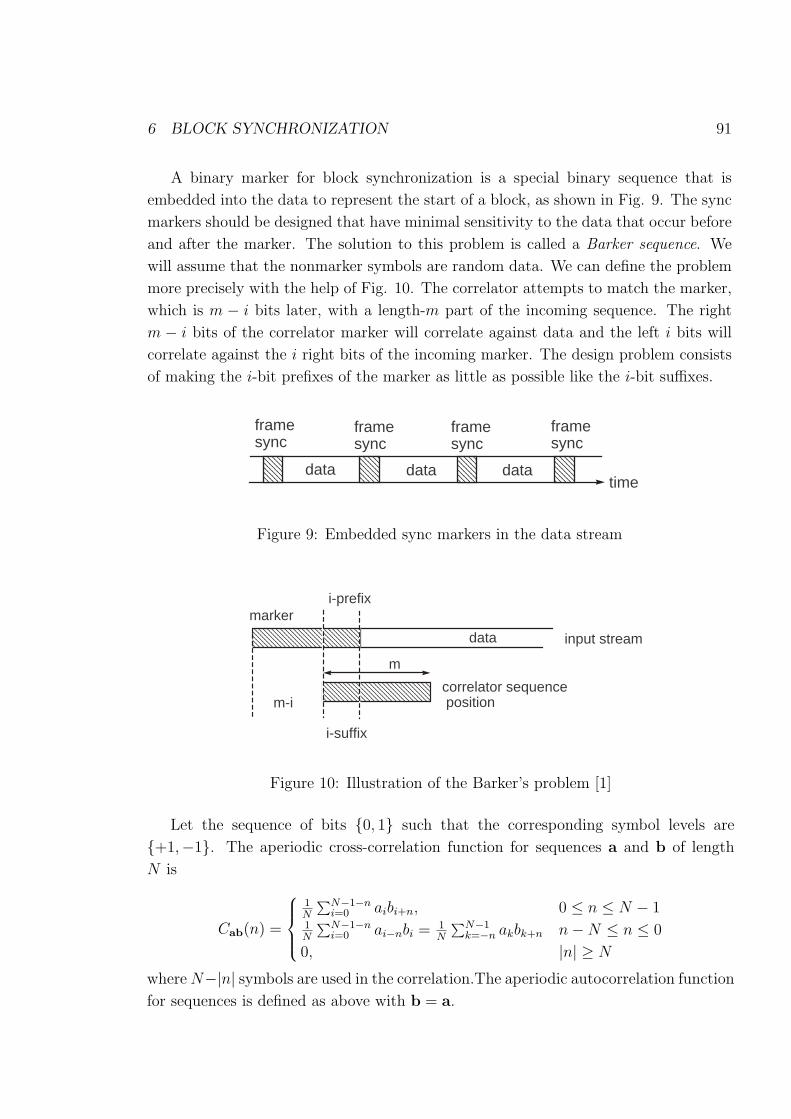
A binary marker for block synchronization is a special binary sequence that is
embedded into the data to represent the start of a block, as shown in Fig. 9. The sync
markers should be designed that have minimal sensitivity to the data that occur before
and after the marker. The solution to this problem is called a Barker sequence. We
will assume that the nonmarker symbols are random data. We can define the problem
more precisely with the help of Fig. 10. The correlator attempts to match the marker,
which is m − i bits later, with a length-m part of the incoming sequence. The right
m − i bits of the correlator marker will correlate against data and the left i bits will
correlate against the i right bits of the incoming marker. The design problem consists
of making the i-bit prefixes of the marker as little as possible like the i-bit suffixes.
xxxxxxxxxxxxxxxxxxxxxxxxxxxxxxxxxxx
xxxxxxxxxxxxxxxxxxxxxxxxxxxxxxxxxxx
xxxxxxxxxxxxxxxxxxxxxxxxxxxxxxxxxxx
xxxxxxxxxxxxxxxxxxxxxxxxxxxxxxxxxxx
data data data
framesync
framesync
framesync
framesync
time
Figure 9: Embedded sync markers in the data stream
xxxxxxxxxxxxxxxxxxxxxxxxxxxxxxxxxxxxxxxxxxxxxxxxxxxxxxxxxxxxxxxxxxxxxxxxxxxxxxxxxxxxxxxxxxxxxxxxxxxxxxxxxxxxxxxxxxxxxxxxxxxxx
xxxxxxxxxxxxxxxxxxxxxxxxxxxxxxxxxxxxxxxxxxxxxxxxxxxxxxxxxxxxxxxxxxxxxxxxxxxxxxxxxxxxxxxxxxxxxxxxxxxxxxxxxxxxxxxxxxxxxxxxxxxxxxxxxx
marker
xxxxxxxxxxxxxxxxxxxxxxxxxx
xxxxxxxxxxxxxxxxxxxxxxxxxx
i-prefix
i-suffixxxxxxxxxxxxxxxxxxxxx
m-i
xxxxxxxxxxxxxxxxxxxxxx
m
data
correlator sequence position
input stream
Figure 10: Illustration of the Barker’s problem [1]
Let the sequence of bits {0, 1} such that the corresponding symbol levels are
{+1,−1}. The aperiodic cross-correlation function for sequences a and b of length
N is
Cab(n) =
1N
∑N−1−ni=0 aibi+n, 0 ≤ n ≤ N − 1
1N
∑N−1−ni=0 ai−nbi = 1
N
∑N−1k=−n akbk+n n−N ≤ n ≤ 0
0, |n| ≥ N
where N−|n| symbols are used in the correlation.The aperiodic autocorrelation function
for sequences is defined as above with b = a.
7 NONCOHERENT DETECTION 92
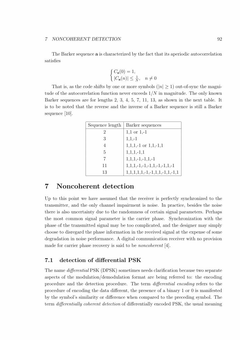
The Barker sequence a is characterized by the fact that its aperiodic autocorrelation
satisfies
{Ca(0) = 1,
|Ca(n)| ≤ 1N
, n 6= 0
That is, as the code shifts by one or more symbols (|n| ≥ 1) out-of-sync the magni-
tude of the autocorrelation function never exceeds 1/N in magnitude. The only known
Barker sequences are for lengths 2, 3, 4, 5, 7, 11, 13, as shown in the next table. It
is to be noted that the reverse and the inverse of a Barker sequence is still a Barker
sequence [10].
Sequence length Barker sequences
2 1,1 or 1,-1
3 1,1,-1
4 1,1,1,-1 or 1,1,-1,1
5 1,1,1,-1,1
7 1,1,1,-1,-1,1,-1
11 1,1,1,-1,-1,-1,1,-1,-1,1,-1
13 1,1,1,1,1,-1,-1,1,1,-1,1,-1,1
7 Noncoherent detection
Up to this point we have assumed that the receiver is perfectly synchronized to the
transmitter, and the only channel impairment is noise. In practice, besides the noise
there is also uncertainty due to the randomness of certain signal parameters. Perhaps
the most common signal parameter is the carrier phase. Synchronization with the
phase of the transmitted signal may be too complicated, and the designer may simply
choose to disregard the phase information in the received signal at the expense of some
degradation in noise performance. A digital communication receiver with no provision
made for carrier phase recovery is said to be noncoherent [4].
7.1 detection of differential PSK
The name differential PSK (DPSK) sometimes needs clarification because two separate
aspects of the modulation/demodulation format are being referred to: the encoding
procedure and the detection procedure. The term differential encoding refers to the
procedure of encoding the data different, the presence of a binary 1 or 0 is manifested
by the symbol’s similarity or difference when compared to the preceding symbol. The
term differentially coherent detection of differentially encoded PSK, the usual meaning
7 NONCOHERENT DETECTION 93
of DPSK, refers to a detection scheme classified as noncoherent because it does not
require a reference in phase with the received carrier.
With noncoherent systems, no attempt is made to determine the actual value of
the phase of the incoming signal. Thus, if the transmitted waveform is
si(t) =
√2Es
Ts
cos[ω0t + θi(t)], 0 ≤ t ≤ Ts, i = 0, . . . , M − 1
where Es is the symbol energy and the received signal can be characterized by
r(t) =
√2E
Tcos[ω0t + θi(t) + α] + w(t), 0 ≤ t ≤ T, i = 0, . . . ,M − 1
where α is an arbitrary constant and is typically assumed to be a random variable
uniformly distributed in [0, 2π[, and w(t) is an AWGN process.
For coherent detection, matched filters (or their equivalents) are used; for nonco-
herent detection, this is not possible because α is not known. However, if we assume
that α varies slowly relative to two period times (2T ), the phase difference between
two successive waveforms, θj(T1) and θk(T2) is independent of α.
The essence of differentially coherent detection of differentially encoded PSK (DPSK)
is that the identity of the data is inferred from the changes in phase from symbol to
symbol. Therefore, since the data are detected by differentially examining the wave-
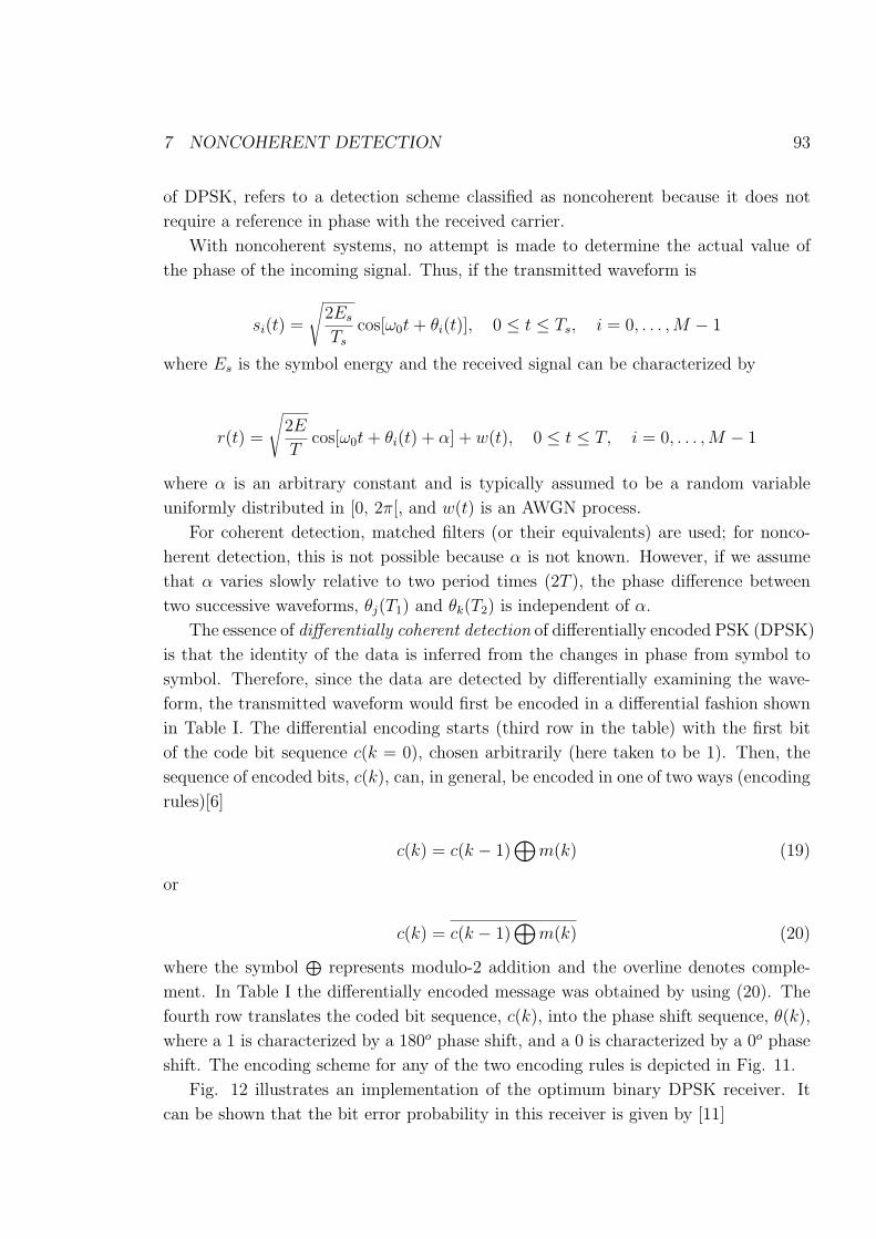
form, the transmitted waveform would first be encoded in a differential fashion shown
in Table I. The differential encoding starts (third row in the table) with the first bit
of the code bit sequence c(k = 0), chosen arbitrarily (here taken to be 1). Then, the
sequence of encoded bits, c(k), can, in general, be encoded in one of two ways (encoding
rules)[6]
c(k) = c(k − 1)⊕
m(k) (19)
or
c(k) = c(k − 1)⊕
m(k) (20)
where the symbol⊕
represents modulo-2 addition and the overline denotes comple-
ment. In Table I the differentially encoded message was obtained by using (20). The
fourth row translates the coded bit sequence, c(k), into the phase shift sequence, θ(k),
where a 1 is characterized by a 180o phase shift, and a 0 is characterized by a 0o phase
shift. The encoding scheme for any of the two encoding rules is depicted in Fig. 11.
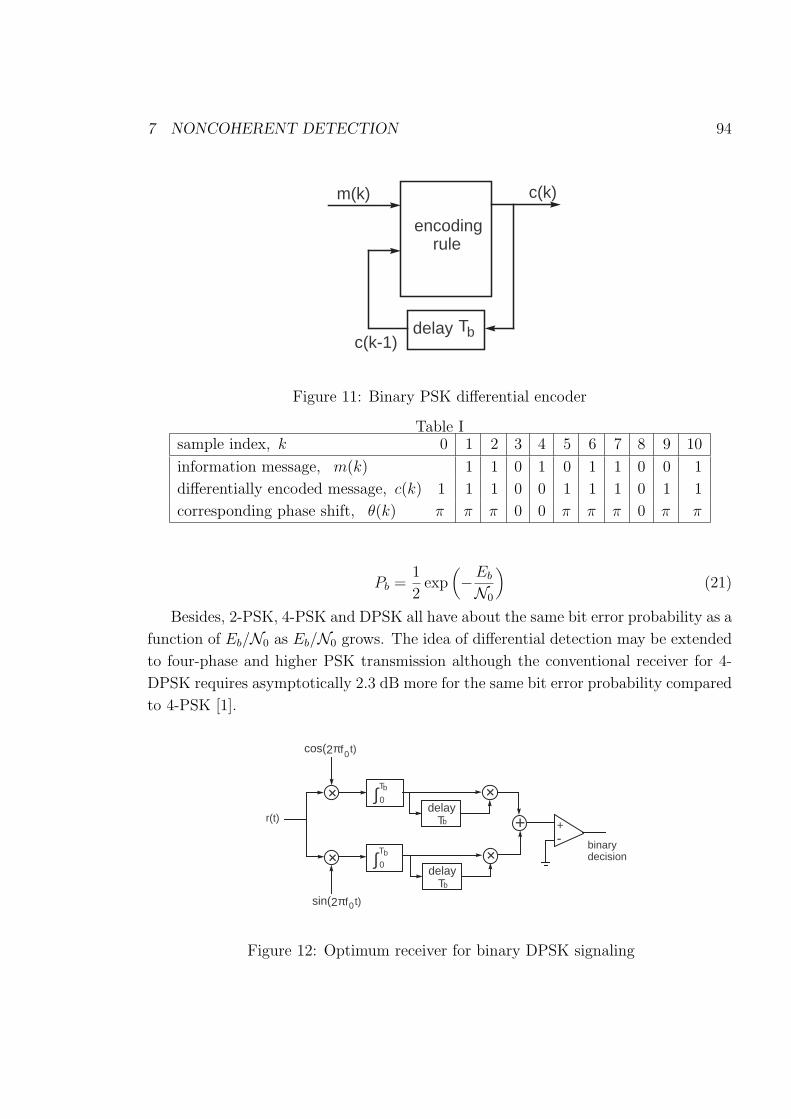
Fig. 12 illustrates an implementation of the optimum binary DPSK receiver. It
can be shown that the bit error probability in this receiver is given by [11]
7 NONCOHERENT DETECTION 94
encoding rule
delay Tb
c(k)m(k)
c(k-1)
Figure 11: Binary PSK differential encoder
Table Isample index, k 0 1 2 3 4 5 6 7 8 9 10
information message, m(k) 1 1 0 1 0 1 1 0 0 1
differentially encoded message, c(k) 1 1 1 0 0 1 1 1 0 1 1
corresponding phase shift, θ(k) π π π 0 0 π π π 0 π π
Pb =1
2exp
(−Eb
N0
)(21)
Besides, 2-PSK, 4-PSK and DPSK all have about the same bit error probability as a
function of Eb/N0 as Eb/N0 grows. The idea of differential detection may be extended
to four-phase and higher PSK transmission although the conventional receiver for 4-
DPSK requires asymptotically 2.3 dB more for the same bit error probability compared
to 4-PSK [1].
fcos(2π t)
+delay T
+
r(t)
∫0
T
+- binary
decision+
0
f sin(2π t)0
∫0
T
delay T
+
+
b
b
b
b
Figure 12: Optimum receiver for binary DPSK signaling
7 NONCOHERENT DETECTION 95
7.2 noncoherent detection over the AWGN channel
Assume that there are M signaling waveforms used in the transmission of information,
namely
sm(t) = Re[um(t)ej2πf0t], m = 0, ..., M − 1
where {um(t)} are the (baseband) complex envelopes. The channel is assumed to
introduce an attenuation factor α and a phase shift φm for each signal. The phases
{φm} are assumed to be mutually statistically independent and uniformly distributed
in the interval [0, 2π[.
Consider that symbol sk(t) was transmitted. The received signal is
r(t) = Re{αejφmuk(t)ej2πf0t + n(t)ej2πf0t}
The complex envelope of the received signal is
x(t) = αe−jφmum(t) + z(t) + nR(t) + jnI(t)
where nR(t) and nI(t) are the inphase and quadrature components of the noise. It was
shown in [2] that the optimum receiver for AWGN channels and equally likely signals
with equal energy computes the M decision variables
|Zm| =∣∣∣∣∣∫ T
0x(t)u∗m(t) dt
∣∣∣∣∣ , m = 0, . . . , M − 1
and selects the signal corresponding to the largest decision variable.
Thus
Zm =∫ T
0[xR(t) + jxI(t)][um,R(t) + um,I(t)] dt
and doing Zm = Zm,R + jZm,I leads to
Zm,R =∫ T
0[xR(t)um,R(t) + xI(t)um,I(t)] dt
Zm,I =∫ T
0[xI(t)um,R(t)− xR(t)um,I(t)] dt
The optimum detector, based on a random, uniformly distributed carrier phase,
computes the M envelopes
|Zm| =√
Z2m,R + Z2
m,I , m = 0, . . . , M − 1 (22)
7 NONCOHERENT DETECTION 96
or equivalently the squared envelopes |Zm|2 and selects the signal with the largest
envelope (or squared envelope).
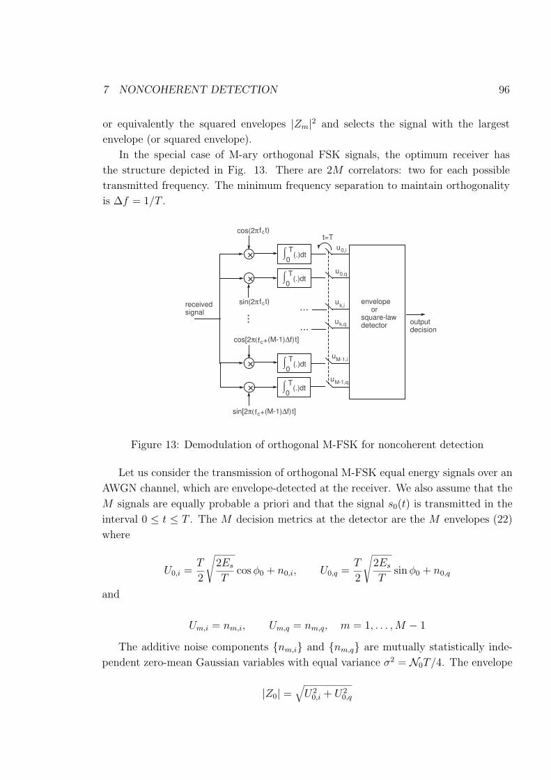
In the special case of M-ary orthogonal FSK signals, the optimum receiver has
the structure depicted in Fig. 13. There are 2M correlators: two for each possible
transmitted frequency. The minimum frequency separation to maintain orthogonality
is ∆f = 1/T .
+
+
cos(2πfc t)
sin(2πfc t)
∫0
T(.)dt
∫0
T(.)dt
+
+
cos[2π(fc t]
∫0
T(.)dt
∫0
T(.)dt
receivedsignal
...
...+ ∆(M-1) f)
sin[2π(fc t]+ ∆(M-1) f)
envelope or square-lawdetector
outputdecision
t=T
...
u
u
u
u
u
u
0,i
0,q
k,i
k,q
M-1,i
M-1,q
Figure 13: Demodulation of orthogonal M-FSK for noncoherent detection
Let us consider the transmission of orthogonal M-FSK equal energy signals over an
AWGN channel, which are envelope-detected at the receiver. We also assume that the
M signals are equally probable a priori and that the signal s0(t) is transmitted in the
interval 0 ≤ t ≤ T . The M decision metrics at the detector are the M envelopes (22)
where
U0,i =T
2
√2Es
Tcos φ0 + n0,i, U0,q =
T
2
√2Es
Tsin φ0 + n0,q
and
Um,i = nm,i, Um,q = nm,q, m = 1, . . . , M − 1
The additive noise components {nm,i} and {nm,q} are mutually statistically inde-
pendent zero-mean Gaussian variables with equal variance σ2 = N0T/4. The envelope
|Z0| =√
U20,i + U2
0,q
7 NONCOHERENT DETECTION 97
is characterized by a Rice distribution with pdf
p|Z0|(r) =r
σ2exp
(−r2 + s2
2σ2
)I0
(rs
σ2
), r ≥ 0
where the noncentrality parameter is
s2 = (E{U0,i})2 + (E{U0,q})2 =TEs
2
and I0(x) is the zeroth-order modified Bessel function of the first kind.
Besides, the remaining envelopes
|Zk| =√
U2k,i + U2
k,q, k = 1, . . . , M − 1
are characterized by Rayleigh distributions with pdf
p|Zk|(r) =r
σ2exp
(− r2
2σ2
), r ≥ 0
It can be shown that the probability of a symbol error is [2]
Ps =M−1∑
n=1
(−1)n+1
(M − 1
n
)1
n + 1exp
[− nEs
(n + 1)N0
](23)
For binary orthogonal signals (M = 2) equation (23) reduces to the simple form
Pb =1
2exp
(− Eb
2N0
)(24)
For M > 2, we may compute the bit error probability by making use of the rela-
tionship
Pb =M/2
M − 1Ps
This expression has the same asymptotic energy efficiency as Q(√
Eb/N0), the error
probability of coherent orthogonal 2-FSK. A similar conclusion applies with M-ary
orthogonal signaling. Thus, noncoherent detection of orthogonal M-FSK in a good
AWGN channel (Eb/N0 À 1) leads to no real loss in energy efficiency [1].
It can be shown that binary DPSK signals are orthogonal over a two-bit interval
[4], [6]. Thus, equation (21) results from (24) by considering that the energy in the
two-bit interval is 2Eb.
REFERENCES 98
References
[1] John B. Anderson, “Digital Transmission Engineering”, IEEE Press, N. York,
1999.
[2] John G. Proakis, “Digital Comunications”, third edition, McGraw-Hill, N. York,
1995.
[3] Leon W. Couch II, “Digital and Analog Communication Systems”, Macmillan, N.
York, 1990.
[4] Simon Haykin, “Communication Systems”, 4.th edition, Wiley, N. York, 2001.
[5] Sergio Benedetto and Ezio Biglieri, “Principles of Digital Transmission with Wire-
less Applications”, Kluwer, N. York, 1999.
[6] Bernard Sklar, “Digital Communications. Fundamentals and Aplications”,
Prentice-Hall, Englewood Cliffs, N.J., 1988.
[7] Richard E. Blahut, “Digital Transmission of Information”, Addison-Wesley, Read-
ing, MA, 1990.
[8] Kamilo Feher, “Digital Communications: microwave applications”, Prentice-Hall,
Englewood Cliffs, NJ, 1981.
[9] Steven M. Kay, “Fundamentals of Statistical Signal Processing: Estimation The-
ory”, Prentice Hall, Upper Saddle River, NJ, 1993.
[10] Jack K. Holmes, “Spread Spectrum Systems for GNSS and Wireless Communica-
tions”, Artech House, Norwood, MA, 2007.
[11] Marvin K. Simon, Sami M, Hinedi, William C. Linsey, “Digital Communication
Techniques”, Prentice-Hall, Englewood Cliffs, NJ, 1995.


![pairs in the e -jet nal state with ˝˝ events at...to the Handbook of LHC Higgs Cross Sections (entry [40] in the Bibliography). The measurement of the ˝trigger e ciency in Section4.3.2and](https://static.fdocument.org/doc/165x107/61452c3b34130627ed50d0cc/pairs-in-the-e-jet-nal-state-with-events-at-to-the-handbook-of-lhc-higgs.jpg)