
IRSM5(0,1)5-015 Series
15
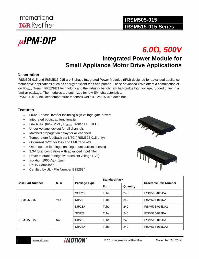
IRSM505-015 IRSM515-015 Series 1 www.irf.com © 2014 International Rectifier November 24, 2014 6.0Ω, 500V Integrated Power Module for Small Appliance Motor Drive Applications Description IRSM505-015 and IRSM515-015 are 3-phase Integrated Power Modules (IPM) designed for advanced appliance motor drive applications such as energy efficient fans and pumps. These advanced IPMs offers a combination of low R DS(on) Trench FREDFET technology and the industry benchmark half-bridge high voltage, rugged driver in a familiar package. The modules are optimized for low EMI characteristics. IRSM505-015 includes temperature feedback while IRSM515-015 does not. Features 500V 3-phase inverter including high voltage gate drivers Integrated bootstrap functionality Low 6.0Ω (max, 25°C) R DS(on) Trench FREDFET Under-voltage lockout for all channels Matched propagation delay for all channels Temperature feedback via NTC (IRSM505-015 only) Optimized dV/dt for loss and EMI trade offs Open-source for single and leg-shunt current sensing 3.3V logic compatible with advanced input filter Driver tolerant to negative transient voltage (-Vs) Isolation 1900V RMS , 1min RoHS Compliant Certified by UL - File Number E252584 Base Part Number NTC Package Type Standard Pack Orderable Part Number Form Quantity IRSM505-015 Yes SOP23 Tube 240 IRSM505-015PA DIP23 Tube 240 IRSM505-015DA DIP23A Tube 240 IRSM505-015DA2 IRSM515-015 No SOP23 Tube 240 IRSM515-015PA DIP23 Tube 240 IRSM515-015DA DIP23A Tube 240 IRSM515-015DA2
Transcript of IRSM5(0,1)5-015 Series
IRSM505-015
IRSM515-015 Series
1 www.irf.com © 2014 International Rectifier November 24, 2014
6.0Ω, 500V
Integrated Power Module for Small Appliance Motor Drive Applications
Description
IRSM505-015 and IRSM515-015 are 3-phase Integrated Power Modules (IPM) designed for advanced appliance
motor drive applications such as energy efficient fans and pumps. These advanced IPMs offers a combination of
low RDS(on) Trench FREDFET technology and the industry benchmark half-bridge high voltage, rugged driver in a
familiar package. The modules are optimized for low EMI characteristics.
IRSM505-015 includes temperature feedback while IRSM515-015 does not.
Features
500V 3-phase inverter including high voltage gate drivers
Integrated bootstrap functionality
Low 6.0Ω (max, 25°C) RDS(on) Trench FREDFET
Under-voltage lockout for all channels
Matched propagation delay for all channels
Temperature feedback via NTC (IRSM505-015 only)
Optimized dV/dt for loss and EMI trade offs
Open-source for single and leg-shunt current sensing
3.3V logic compatible with advanced input filter
Driver tolerant to negative transient voltage (-Vs)
Isolation 1900VRMS, 1min
RoHS Compliant
Certified by UL - File Number E252584
Base Part Number NTC Package Type Standard Pack
Orderable Part Number Form Quantity
IRSM505-015 Yes
SOP23 Tube 240 IRSM505-015PA
DIP23 Tube 240 IRSM505-015DA
DIP23A Tube 240 IRSM505-015DA2
IRSM515-015 No
SOP23 Tube 240 IRSM515-015PA
DIP23 Tube 240 IRSM515-015DA
DIP23A Tube 240 IRSM515-015DA2
IRSM505-015 IRSM515-015 Series
2 www.irf.com © 2014 International Rectifier November 24, 2014
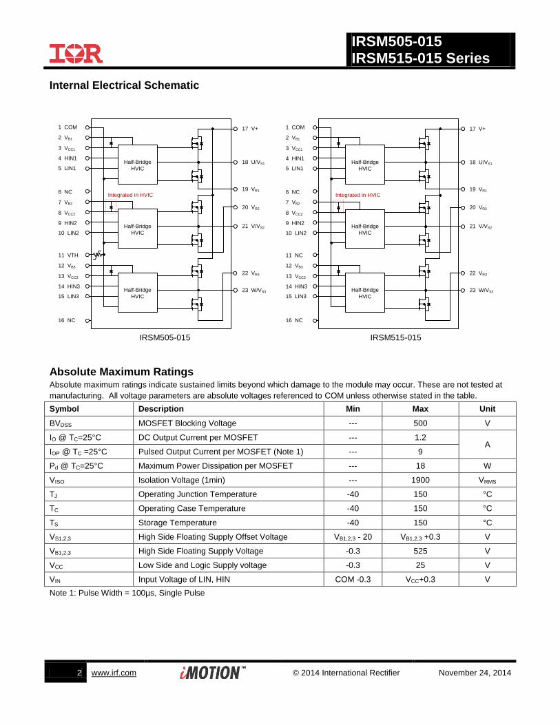
Internal Electrical Schematic
Half-Bridge
HVIC
Half-Bridge
HVIC
Half-Bridge
HVIC
1 COM
2 VB1
3 VCC1
4 HIN1
5 LIN1
6 NC
7 VB2
8 VCC2
9 HIN2
10 LIN2
11 VTH
12 VB3
13 VCC3
14 HIN3
15 LIN3
16 NC
17 V+
18 U/VS1
19 VR1
20 VR2
21 V/VS2
22 VR3
23 W/VS3
Integrated in HVIC
Half-Bridge
HVIC
Half-Bridge
HVIC
Half-Bridge
HVIC
1 COM
2 VB1
3 VCC1
4 HIN1
5 LIN1
6 NC
7 VB2
8 VCC2
9 HIN2
10 LIN2
11 NC
12 VB3
13 VCC3
14 HIN3
15 LIN3
16 NC
17 V+
18 U/VS1
19 VR1
20 VR2
21 V/VS2
22 VR3
23 W/VS3
Integrated in HVIC
IRSM505-015 IRSM515-015
Absolute Maximum Ratings Absolute maximum ratings indicate sustained limits beyond which damage to the module may occur. These are not tested at
manufacturing. All voltage parameters are absolute voltages referenced to COM unless otherwise stated in the table.
Symbol Description Min Max Unit
BVDSS MOSFET Blocking Voltage --- 500 V
IO @ TC=25°C DC Output Current per MOSFET --- 1.2 A
IOP @ TC =25°C Pulsed Output Current per MOSFET (Note 1) --- 9
Pd @ TC=25°C Maximum Power Dissipation per MOSFET --- 18 W
VISO Isolation Voltage (1min) --- 1900 VRMS
TJ Operating Junction Temperature -40 150 °C
TC Operating Case Temperature -40 150 °C
TS Storage Temperature -40 150 °C
VS1,2,3 High Side Floating Supply Offset Voltage VB1,2,3 - 20 VB1,2,3 +0.3 V
VB1,2,3 High Side Floating Supply Voltage -0.3 525 V
VCC Low Side and Logic Supply voltage -0.3 25 V
VIN Input Voltage of LIN, HIN COM -0.3 VCC+0.3 V
Note 1: Pulse Width = 100µs, Single Pulse
IRSM505-015 IRSM515-015 Series
3 www.irf.com © 2014 International Rectifier November 24, 2014
Recommended Operating Conditions
Symbol Description Min Max Unit
V+ Positive DC Bus Input Voltage --- 400 V
VS1,2,3 High Side Floating Supply Offset Voltage (Note 2) 400 V
VB1,2,3 High Side Floating Supply Voltage VS+12 VS+20 V
VCC Low Side and Logic Supply Voltage 13.5 16.5 V
VIN Input Voltage of LIN, HIN, ITRIP, EN, FLT 0 5 V
Fp PWM Carrier Frequency --- 20 kHz
Note 2: Logic operational for Vs from COM-8V to COM+500V. Logic state held for Vs from COM-8V to COM-VBS.
Static Electrical Characteristics (VCC-COM) = (VB-VS) = 15 V. TC = 25
oC unless otherwise specified. The VIN and IIN parameters are referenced to COM and
are applicable to all six channels. The VCCUV parameters are referenced to COM. The VBSUV
parameters are referenced to VS.
Symbol Description Min Typ Max Units Conditions
BVDSS Drain-to-Source Breakdown Voltage 500 --- --- V TJ=25°C, ILK=250µA
ILKH Leakage Current of High Side FET 12 µA TJ=25°C, VDS=500V
ILKL Leakage Current of Low Side FET Plus Gate Drive IC
14 µA TJ=25°C, VDS=500V
RDS(on) Drain to Source ON Resistance
--- 5.0 6.0 Ω TJ=25°C, VCC=15V, Id=0.5A
--- 12.3 --- Ω TJ=150°C, VCC=15V, Id=0.5A (Note 3)
VSD Mosfet Body Diode Forward Voltage --- 0.8 --- V TJ=25°C, VCC=15V, ID=0.5A
VIN,th+ Positive Going Input Threshold 2.2 --- --- V
VIN,th- Negative Going Input Threshold --- --- 0.8 V
VCCUV+,
VBSUV+ VCC and VBS Supply Under-Voltage, Positive Going Threshold
8 8.9 9.8 V
VCCUV-,
VBSUV- VCC and VBS supply Under-Voltage, Negative Going Threshold
6.9 7.7 8.5 V
VCCUVH,
VBSUVH VCC and VBS Supply Under-Voltage Lock-Out Hysteresis
--- 1.2 --- V
IQBS Quiescent VBS Supply Current VIN=0V --- 42 60 µA
IQBS, ON Quiescent VBS Supply Current VIN=4V --- 42 60 µA
IQCC Quiescent VCC Supply Current VIN=0V --- 1.7 4 mA
IQCC, ON Quiescent VCC Supply Current VIN=4V --- 1.8 4 mA
IIN+ Input Bias Current VIN=4V --- 5.9 18 µA VIN=3.3V
IIN- Input Bias Current VIN=0V --- --- 2 µA VIN=0V
RBR Internal Bootstrap Equivalent Resistor Value
--- 250 --- Ω TJ=25°C
Note 3: Characterized, not tested at manufacturing
IRSM505-015 IRSM515-015 Series
4 www.irf.com © 2014 International Rectifier November 24, 2014
Dynamic Electrical Characteristics
(VCC-COM) = (VB-VS) = 15 V. TC = 25oC unless otherwise specified.
Symbol Description Min Typ Max Units Conditions
TON Input to Output Propagation Turn-On Delay Time
--- 0.7 1.5 µs ID=120mA, V+=30V See Fig.1
TOFF Input to Output Propagation Turn-Off Delay Time
--- 0.9 1.5 µs
TFIL,IN Input Filter Time (HIN, LIN) 200 300 --- ns VIN=0 & VIN=3.3V
DT Deadtime Inserted --- 400 --- ns VIN=0 & VIN=3.3V without external deadtime
EON Turn-on switching energy loss --- 17 --- µJ V+=320V, ID=0.3A, L=40mH, TC=25°C (Note 4)
EOFF Turn-off switching energy loss --- 3 --- µJ
EREC Recovery energy loss --- 4 --- µJ
EON,150 Turn-on switching energy loss --- 30 --- µJ V+=320V, ID=0.3A, L=40mH, TC=150°C (Note 4)
EOFF,150 Turn-off switching energy loss --- 4 --- µJ
EREC,150 Recovery energy loss --- 9 --- µJ
Note 4: Characterized, not tested at manufacturing
Thermal and Mechanical Characteristics
Symbol Description Min Typ Max Units Conditions
Rth(J-C) Junction to Case Thermal Resistance --- 7.4 --- °C/W High Side V-Phase Mosfet (Note 5)
Note 5: Characterized, not tested at manufacturing. Case temperature (TC) point shown in Figure 2.
Internal NTC – Thermistor Characteristics (IRSM505-015 Only)
Symbol Description Min Typ Max Units Conditions
R25 Resistance --- 47 --- kΩ TC=25°C, ±5% tolerance
R125 Resistance --- 1.41 --- kΩ TC=125°C
B B-constant (25-50°C) --- 4050 --- K ±2% tolerance (Note 6)
Temperature Range -40 --- 125 °C
Note 6: See application notes for usage
IRSM505-015 IRSM515-015 Series
5 www.irf.com © 2014 International Rectifier November 24, 2014
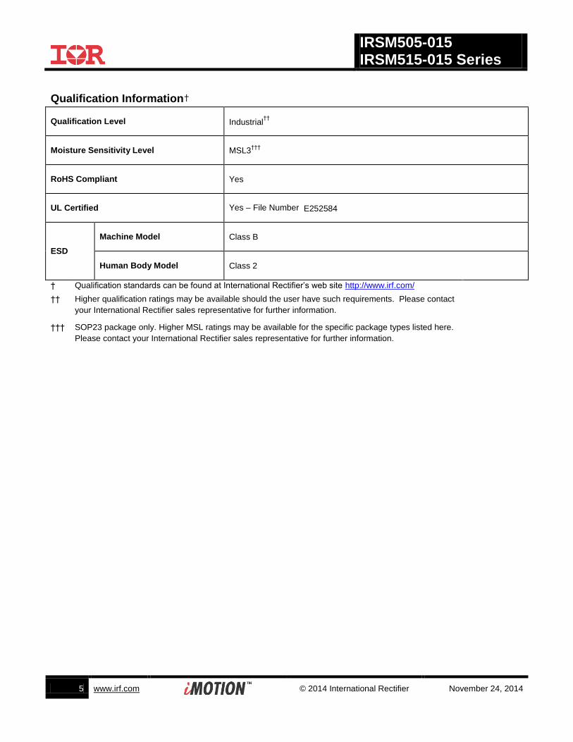
Qualification Information†
Qualification Level Industrial††
Moisture Sensitivity Level MSL3†††
RoHS Compliant Yes
UL Certified Yes – File Number E252584
ESD
Machine Model Class B
Human Body Model Class 2
† Qualification standards can be found at International Rectifier’s web site http://www.irf.com/
†† Higher qualification ratings may be available should the user have such requirements. Please contact
your International Rectifier sales representative for further information.
††† SOP23 package only. Higher MSL ratings may be available for the specific package types listed here.
Please contact your International Rectifier sales representative for further information.
IRSM505-015 IRSM515-015 Series
6 www.irf.com © 2014 International Rectifier November 24, 2014
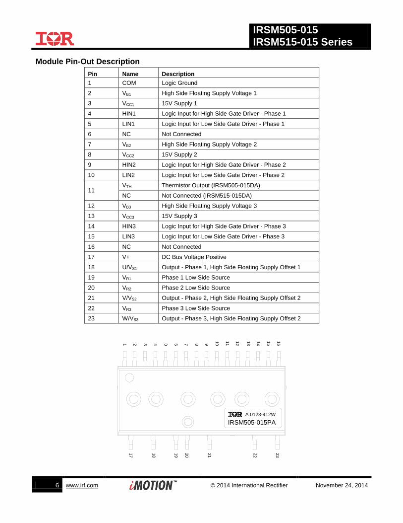
Module Pin-Out Description
Pin Name Description
1 COM Logic Ground
2 VB1 High Side Floating Supply Voltage 1
3 VCC1 15V Supply 1
4 HIN1 Logic Input for High Side Gate Driver - Phase 1
5 LIN1 Logic Input for Low Side Gate Driver - Phase 1
6 NC Not Connected
7 VB2 High Side Floating Supply Voltage 2
8 VCC2 15V Supply 2
9 HIN2 Logic Input for High Side Gate Driver - Phase 2
10 LIN2 Logic Input for Low Side Gate Driver - Phase 2
11 VTH Thermistor Output (IRSM505-015DA)
NC Not Connected (IRSM515-015DA)
12 VB3 High Side Floating Supply Voltage 3
13 VCC3 15V Supply 3
14 HIN3 Logic Input for High Side Gate Driver - Phase 3
15 LIN3 Logic Input for Low Side Gate Driver - Phase 3
16 NC Not Connected
17 V+ DC Bus Voltage Positive
18 U/VS1 Output - Phase 1, High Side Floating Supply Offset 1
19 VR1 Phase 1 Low Side Source
20 VR2 Phase 2 Low Side Source
21 V/VS2 Output - Phase 2, High Side Floating Supply Offset 2
22 VR3 Phase 3 Low Side Source
23 W/VS3 Output - Phase 3, High Side Floating Supply Offset 2
1
2
3
4
0 6
7
8
9
10
11
12
13
14
15
16
2
3
22
21
20
19
18
17
A 0123-412W
IRSM505-015PA
IRSM505-015 IRSM515-015 Series
7 www.irf.com © 2014 International Rectifier November 24, 2014
Referenced Figures
Figure 2: TC measurement point for Rth(j-C)
3.8mm
14.5mm
Top View
TC
Figure 1a: Input to Output propagation turn-on
delay time.
Figure 1b: Input to Output propagation turn-off
delay time.
Figure 1c: Diode Reverse Recovery.
Figure 1: Switching Parameter Definitions
50%
HIN /LIN
VCEIC
HIN /LIN
TOFF
tf
90 % IC
10 % IC
50%
VCE
VCE IC
HIN /LIN
TON
tr
50%
HIN /LIN
90 % IC
10 % IC
50%
VCE
VCE
IF
HIN/LIN
trr
Irr
IRSM505-015 IRSM515-015 Series
8 www.irf.com © 2014 International Rectifier November 24, 2014
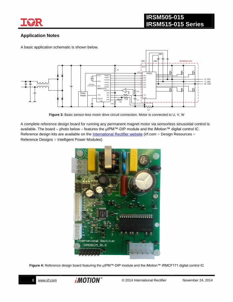
Application Notes
A basic application schematic is shown below.
HVICsVCC
HIN1
HIN2
HIN3
LIN1
LIN2
LIN3
VTH
VB1
VB2
VB3
U, VS1
V, VS2W, VS3
Power
Supply
PWMWH
PWMVH
PWMUH
PWMVL
PWMWL
GATEKILL
AIN1
IFB+
IFB-
IFBOVSS
VDD
VDDCAP
XTAL0
XTAL1
AIN2SPD-REF
COM
VBUS
IRMCF171
PWMUL
4.87k
2M
7.50k
1nF
0.25
6.04k
7.68k
+
-
3V
IRSM505-015x
Figure 3: Basic sensor-less motor drive circuit connection. Motor is connected to U, V, W
A complete reference design board for running any permanent magnet motor via sensorless sinusoidal control is
available. The board – photo below – features the µIPM™-DIP module and the iMotion™ digital control IC.
Reference design kits are available on the International Rectifier website (irf.com > Design Resources >
Reference Designs > Intelligent Power Modules)
Figure 4: Reference design board featuring the µIPM™-DIP module and the iMotion™ IRMCF171 digital control IC
IRSM505-015 IRSM515-015 Series
9 www.irf.com © 2014 International Rectifier November 24, 2014
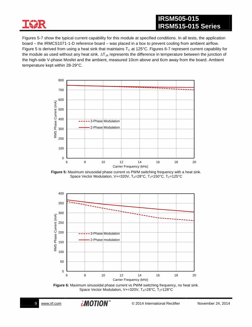
Figures 5-7 show the typical current capability for this module at specified conditions. In all tests, the application
board – the IRMCS1071-1-D reference board – was placed in a box to prevent cooling from ambient airflow.
Figure 5 is derived from using a heat sink that maintains TC at 125°C. Figures 6-7 represent current capability for
the module as used without any heat sink. ∆TJA represents the difference in temperature between the junction of
the high-side V-phase Mosfet and the ambient, measured 10cm above and 6cm away from the board. Ambient
temperature kept within 28-29°C.
Figure 5: Maximum sinusoidal phase current vs PWM switching frequency with a heat sink.
Space Vector Modulation, V+=320V, TA=28°C, TJ=150°C, TC=125°C
Figure 6: Maximum sinusoidal phase current vs PWM switching frequency, no heat sink.
Space Vector Modulation, V+=320V, TA=28°C, TJ=128°C
0
100
200
300
400
500
600
700
800
6 8 10 12 14 16 18 20
RM
S P
hase C
urr
ent
(mA
)
Carrier Frequency (kHz)
3-Phase Modulation
2-Phase Modulation
0
50
100
150
200
250
300
350
400
6 8 10 12 14 16 18 20
RM
S P
hase C
urr
ent
(mA
)
Carrier Frequency (kHz)
3-Phase Modulation
2-Phase modulation
IRSM505-015 IRSM515-015 Series
10 www.irf.com © 2014 International Rectifier November 24, 2014
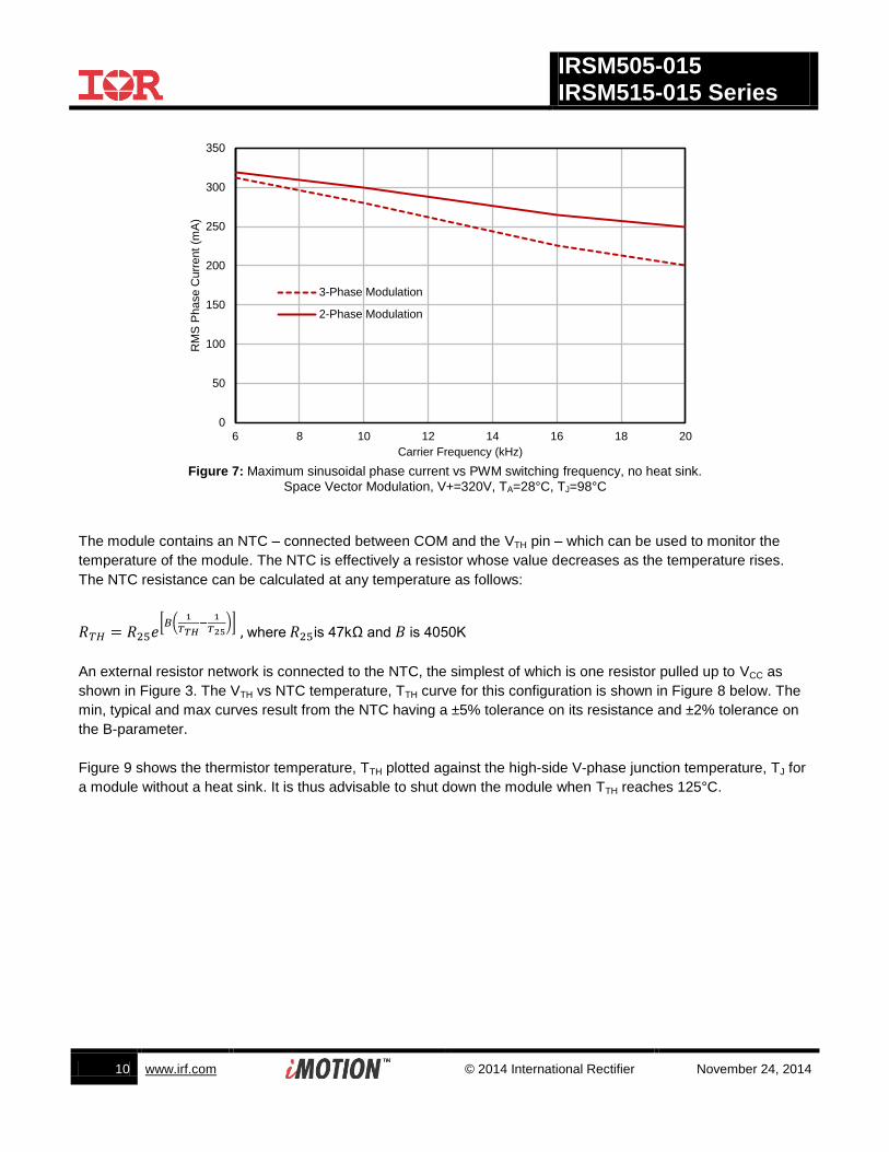
Figure 7: Maximum sinusoidal phase current vs PWM switching frequency, no heat sink.
Space Vector Modulation, V+=320V, TA=28°C, TJ=98°C
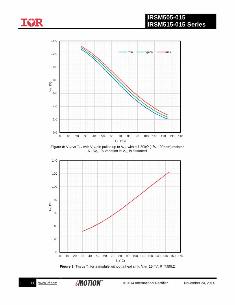
The module contains an NTC – connected between COM and the VTH pin – which can be used to monitor the
temperature of the module. The NTC is effectively a resistor whose value decreases as the temperature rises.
The NTC resistance can be calculated at any temperature as follows:
[ (
)] where is 7 Ω and is 0 0
An external resistor network is connected to the NTC, the simplest of which is one resistor pulled up to VCC as
shown in Figure 3. The VTH vs NTC temperature, TTH curve for this configuration is shown in Figure 8 below. The
min, typical and max curves result from the NTC having a ±5% tolerance on its resistance and ±2% tolerance on
the B-parameter.
Figure 9 shows the thermistor temperature, TTH plotted against the high-side V-phase junction temperature, TJ for
a module without a heat sink. It is thus advisable to shut down the module when TTH reaches 125°C.
0
50
100
150
200
250
300
350
6 8 10 12 14 16 18 20
RM
S P
hase C
urr
ent
(mA
)
Carrier Frequency (kHz)
3-Phase Modulation
2-Phase Modulation
IRSM505-015 IRSM515-015 Series
11 www.irf.com © 2014 International Rectifier November 24, 2014
Figure 8: VTH vs TTH with VTH pin pulled up to VCC with a 7. 0 Ω (1%, 100ppm) resistor.
A 15V, 1% variation in VCC is assumed.
Figure 9: TTH vs TJ for a module without a heat sink. VCC=15.4V, R=7.50kΩ
0.0
2.0
4.0
6.0
8.0
10.0
12.0
14.0
0 10 20 30 40 50 60 70 80 90 100 110 120 130 140
VT
H (
V)
TTH (°C)
min typical max
0
20
40
60
80
100
120
140
0 10 20 30 40 50 60 70 80 90 100 110 120 130 140 150 160
TT
H (°C
TJ (°C)
IRSM505-015 IRSM515-015 Series
12 www.irf.com © 2014 International Rectifier November 24, 2014
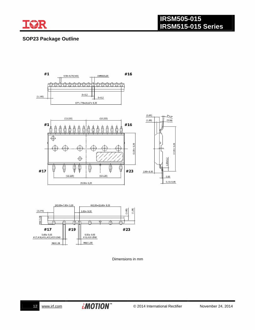
SOP23 Package Outline
Dimensions in mm
IRSM505-015 IRSM515-015 Series
13 www.irf.com © 2014 International Rectifier November 24, 2014
DIP23A Package Outline
Dimensions in mm
IRSM505-015 IRSM515-015 Series
14 www.irf.com © 2014 International Rectifier November 24, 2014
DIP23 Package Outline
Dimensions in mm
IRSM505-015 IRSM515-015 Series
15 www.irf.com © 2014 International Rectifier November 24, 2014
Top Marking
A 0123-412P
IRSM505-015PA
Marking Code P = Pb Free; Y = Engineering Samples
Date Code YWW format, where Y = least significant digit of the production year , WW = two digits representing the week of the production year
Revision History
Nov 2014 Corrected logic in Figure 1. Added UL certification note
Data and Specifications are subject to change without notice
IR WORLD HEADQUARTERS: 233 Kansas St., El Segundo, California 90245, USA Tel: (310) 252-7105
TAC Fax: (310) 252-7903 Visit us at www.irf.com for sales contact information


![y φy ε ,ε ,σ2 t - UW Faculty Web Server · 2006-05-01 · Since the above result holds for any r∈[0,1],one might expect that the result holds uniformly for r∈ [0,1].In fact,](https://static.fdocument.org/doc/165x107/5e2a3a72e3fe3d09b20c3719/y-y-f2-t-uw-faculty-web-server-2006-05-01-since-the-above-result.jpg)