![A Master Project : Searching for a Supersymmetric Higgs ... · 18.03.07 Neal Gueissaz LPHE Projet de Master 3 Théorie 0 0 q i q l q l q i q j q m q n q k h0 m h ∈[93,115] GeV m](https://static.fdocument.org/doc/165x107/5f1c90db415a5a3ff777bef3/a-master-project-searching-for-a-supersymmetric-higgs-180307-neal-gueissaz.jpg)
IO-Link communication master transceiver IC · C/QO, I L+ C/Q O, L+ current (continuous) Internally...
63
November 2017 DocID022817 Rev 6 1/63 This is information on a product in full production. www.st.com L6360 IO-Link communication master transceiver IC Datasheet - production data Features Supply voltage from 18 V to 32.5 V Programmable output stages: high-side, low- side or push-pull (< 2 Ω) Up to 500 mA L+ protected high-side driver COM1, COM2 and COM3 mode supported Additional IEC61131-2 type 1 input Short-circuit and overcurrent output protection through current limitation and programmable cut-off current 3.3 V / 5 V, 50 mA linear regulator 5 mA IO-Link digital input Fast mode I 2 C for IC control, configuration and diagnostic Diagnostic dual LED sequence generator and driver 5 V and 3.3 V compatible I/Os Overvoltage protection (> 36 V) Overtemperature protection ESD protection Miniaturized VFQFPN 26L (3.5x5x1 mm) package Applications Industrial sensors Factory automation Process control Description The L6360 is a monolithic IO-Link master port compliant with PHY2 (3-wire) supporting COM1 (4.8 kbaud), COM2 (38.4 kbaud) and COM3 (230.4 kbaud) modes. The C/QO output stage is programmable: high-side, low-side or push-pull; also cut-off current, cut-off current delay time, and restart delay are programmable. Cut-off current and cut-off current delay time, combined with thermal shutdown and automatic restart, protect the device against overload and short- circuit. C/QO and L+ output stages are able to drive resistive, inductive and capacitive loads. Inductive loads up to 10 mJ can be driven. Supply voltage is monitored and low voltage conditions are detected. The L6360 transfers, through the PHY2(C/QO pin), data received from a host microcontroller through the USART (IN C/QO pin), or to the USART (OUT C/QI pin) data received from PHY2 (C/QI pin). To enable full IC control, configuration and monitoring (i.e. fault conditions stored in the status register), the communication between the system microcontroller and the L6360 is based on a fast mode 2-wire I 2 C. The L6360 has nine registers to manage the programmable parameters and the status of the IC. Monitored fault conditions are: L+ line, overtemperature, C/Q overload, linear regulator undervoltage, and parity check. Internal LED driver circuitries, in open drain configuration, provide two programmable sequences to drive two LEDs.
Transcript of IO-Link communication master transceiver IC · C/QO, I L+ C/Q O, L+ current (continuous) Internally...
November 2017 DocID022817 Rev 6 1/63
This is information on a product in full production. www.st.com
L6360
IO-Link communication master transceiver IC
Datasheet - production data
Features Supply voltage from 18 V to 32.5 V
Programmable output stages: high-side, low-side or push-pull (< 2 Ω)
Up to 500 mA L+ protected high-side driver
COM1, COM2 and COM3 mode supported
Additional IEC61131-2 type 1 input
Short-circuit and overcurrent output protection through current limitation and programmable cut-off current
3.3 V / 5 V, 50 mA linear regulator
5 mA IO-Link digital input
Fast mode I2C for IC control, configuration and diagnostic
Diagnostic dual LED sequence generator and driver
5 V and 3.3 V compatible I/Os
Overvoltage protection (> 36 V)
Overtemperature protection
ESD protection
Miniaturized VFQFPN 26L (3.5x5x1 mm) package
Applications Industrial sensors
Factory automation
Process control
Description The L6360 is a monolithic IO-Link master port compliant with PHY2 (3-wire) supporting COM1 (4.8 kbaud), COM2 (38.4 kbaud) and COM3 (230.4 kbaud) modes. The C/QO output stage is programmable: high-side, low-side or push-pull; also cut-off current, cut-off current delay time, and restart delay are programmable. Cut-off current and cut-off current delay time, combined with thermal shutdown and automatic restart, protect the device against overload and short-circuit. C/QO and L+ output stages are able to drive resistive, inductive and capacitive loads. Inductive loads up to 10 mJ can be driven. Supply voltage is monitored and low voltage conditions are detected. The L6360 transfers, through the PHY2(C/QO pin), data received from a host microcontroller through the USART (IN C/QO pin), or to the USART (OUT C/QI pin) data received from PHY2 (C/QI pin). To enable full IC control, configuration and monitoring (i.e. fault conditions stored in the status register), the communication between the system microcontroller and the L6360 is based on a fast mode 2-wire I2C. The L6360 has nine registers to manage the programmable parameters and the status of the IC. Monitored fault conditions are: L+ line, overtemperature, C/Q overload, linear regulator undervoltage, and parity check. Internal LED driver circuitries, in open drain configuration, provide two programmable sequences to drive two LEDs.
Contents L6360
2/63 DocID022817 Rev 6
Contents
1 Block diagram .................................................................................. 7
2 Pin description ................................................................................ 8
3 Absolute maximum ratings ........................................................... 10
4 Recommended operating conditions ........................................... 11
5 Electrical characteristics .............................................................. 12
6 Device configuration ..................................................................... 19
6.1 Introduction ..................................................................................... 19
6.2 Main features .................................................................................. 19
6.3 General description ......................................................................... 19
6.4 SDA/SCL line control ...................................................................... 19
6.5 Mode selection ................................................................................ 19
6.6 Functional description ..................................................................... 20
6.7 Communication flow ........................................................................ 21
6.8 I2C address ..................................................................................... 21
6.9 Internal register ............................................................................... 22
6.10 Start-up default configuration .......................................................... 32
6.11 Interrupt ........................................................................................... 34
6.12 Demagnetization ............................................................................. 34
6.12.1 Fast demagnetization ....................................................................... 35
6.12.2 Slow demagnetization ...................................................................... 36
7 I2C protocol .................................................................................... 38
7.1 Protocol configuration ..................................................................... 38
7.2 Operating modes ............................................................................. 38
8 Physical layer communication ..................................................... 48
8.1 Transceiver ..................................................................................... 48
8.2 IEC 61131-2 type 1 digital inputs .................................................... 49
9 Diagnostic LED sequence generator and driver ......................... 50
10 Line regulator ................................................................................ 51
11 Application examples .................................................................... 52
12 EMC protection considerations .................................................... 55
12.1 Supply voltage protection ................................................................ 55
12.2 I/O line protection ............................................................................ 57
L6360 Contents
DocID022817 Rev 6 3/63
13 Package information ..................................................................... 59
13.1 VFQFPN 26L (3.5x5x1 mm) package information ........................... 59
13.2 VFQFPN 26L (3.5x5x1 mm) packing information ............................ 60
13.3 Ordering information ....................................................................... 61
14 Revision history ............................................................................ 62
List of tables L6360
4/63 DocID022817 Rev 6
List of tables
Table 1: Pin description .............................................................................................................................. 8 Table 2: Absolute maximum ratings ......................................................................................................... 10 Table 3: Recommended operating conditions .......................................................................................... 11 Table 4: Thermal data ............................................................................................................................... 11 Table 5: Supply ......................................................................................................................................... 12 Table 6: Electrical characteristics - linear regulator .................................................................................. 15 Table 7: Electrical characteristics - logic inputs and outputs .................................................................... 15 Table 8: Electrical characteristics - LED driving ....................................................................................... 15 Table 9: Electrical characteristics - I2C (fast mode) .................................................................................. 15 Table 10: Main parameter typical variations vs. +/- 1% variation of Rbias value ..................................... 17 Table 11: Register addresses ................................................................................................................... 22 Table 12: ENCGQ: C/Q pull-down enable ................................................................................................ 25 Table 13: Icoq: C/QO HS and LS cut-off current ...................................................................................... 25 Table 14: tdcoq: C/QO HS and LS cut-off current delay time................................................................... 25 Table 15: trcoq: C/QO restart delay time .................................................................................................. 26 Table 16: tdbq: C/QI debounce time ......................................................................................................... 26 Table 17: ENCGI: I/Q pull-down enable ................................................................................................... 26 Table 18: CQPDG: C/Q pull-down generator switching ........................................................................... 27 Table 19: L+COD: L+ cut-off disable ........................................................................................................ 27 Table 20: tDCOL: L+ HS cut-off current delay time .................................................................................. 27 Table 21: tRCOL: L+ restart delay ............................................................................................................ 27 Table 22: Bit 1:0 = tdbi [1:0]: I/Q debounce time ...................................................................................... 28 Table 23: C/Q output stage configuration ................................................................................................. 28 Table 24: Parameter default configuration ............................................................................................... 32 Table 25: Register default configuration ................................................................................................... 32 Table 26: Current write mode direction bit ................................................................................................ 40 Table 27: Sequential write mode direction bit ........................................................................................... 42 Table 28: Read mode: register address ................................................................................................... 43 Table 29: Address register ........................................................................................................................ 46 Table 30: Linear regulator selection pin.................................................................................................... 51 Table 31: Maximum CLOADon L+ for ILOAD= 400 mA ........................................................................... 53 Table 32: Supply voltage protection component description .................................................................... 55 Table 33: Refined supply voltage protection component description ....................................................... 56 Table 34: VH protection component description ....................................................................................... 57 Table 35: Typical protection in IO-Link application component description ............................................. 57 Table 36: IO-Link and SIO application extended protection component description ............................... 58 Table 37: VFQFPN 26L (3.5x5x1.0 mm) package mechanical data ........................................................ 60 Table 38: Ordering information ................................................................................................................. 61 Table 39: Document revision history ........................................................................................................ 62
L6360 List of figures
DocID022817 Rev 6 5/63
List of figures
Figure 1: Block diagram .............................................................................................................................. 7 Figure 2: Pin connection (top through view) ............................................................................................... 8 Figure 3: Rise/fall time test setup ............................................................................................................. 16 Figure 4: Normalized rise and fall time vs. output capacitor value (typ. values in push-pull configuration) .................................................................................................................................................................. 17 Figure 5: A master transmitter addressing a slave receiver with a 7-bit address (the transfer is not changed) ................................................................................................................................................... 20 Figure 6: A master reads data from the slave immediately after the first byte ......................................... 20 Figure 7: Transfer sequencing .................................................................................................................. 21 Figure 8: I2C communication .................................................................................................................... 21 Figure 9: Status register............................................................................................................................ 22 Figure 10: Power-on bit behavior .............................................................................................................. 23 Figure 11: Overtemperature (OVT) bit behavior ....................................................................................... 23 Figure 12: Cut-off behavior ....................................................................................................................... 24 Figure 13: Control register 1 ..................................................................................................................... 25 Figure 14: Control register 2 ..................................................................................................................... 26 Figure 15: Configuration register .............................................................................................................. 28 Figure 16: LED1 registers ......................................................................................................................... 31 Figure 17: LED2 registers ......................................................................................................................... 31 Figure 18: Parity register........................................................................................................................... 31 Figure 19: Power stage, Q2 is not present on L+ output .......................................................................... 35 Figure 20: Fast demagnetization principle schematic. Load connected to L- .......................................... 35 Figure 21: Fast demagnetization waveform. Load connected to L- ......................................................... 36 Figure 22: Slow demagnetization block. Load connected to L- ................................................................ 36 Figure 23: Slow demagnetization waveform. Load connected to GND .................................................... 37 Figure 24: Device initialization .................................................................................................................. 38 Figure 25: Current write mode flow chart procedure ................................................................................ 39 Figure 26: Current write mode frames ...................................................................................................... 40 Figure 27: Sequential write mode flow chart procedure ........................................................................... 41 Figure 28: Sequential write mode frames ................................................................................................. 42 Figure 29: Microcontroller parity check calculus ....................................................................................... 42 Figure 30: Register sequence in sequential write mode ........................................................................... 43 Figure 31: Current read mode flow chart procedure ................................................................................. 44 Figure 32: Current read mode frames ...................................................................................................... 45 Figure 33: Current read communication flow ............................................................................................ 45 Figure 34: Sequential/random read mode ................................................................................................ 45 Figure 35: Sequential/random read communication flow ......................................................................... 46 Figure 36: Block diagram communication mode ...................................................................................... 48 Figure 37: System communication mode ................................................................................................. 48 Figure 38: C/Q or L+ channel cut-off protection ....................................................................................... 49 Figure 39: C/Q or L+ channel current limitation and cut-off protection with latched restart ..................... 49 Figure 40: LED drivers .............................................................................................................................. 50 Figure 41: Linear regulator ....................................................................................................................... 51 Figure 42: Linear regulator principle schematic ........................................................................................ 51 Figure 43: Principal connections ............................................................................................................... 52 Figure 44: Application example (I/Q not used): IO-LINK device supplied by L+ pin ................................ 53 Figure 45: Application example (I/Q not used): IO-Link device supplied by single channel IPS .............. 54 Figure 46: Application example: IO-Link devices supplied by dual channel IPS ...................................... 54 Figure 47: Supply voltage protection with uni-directional Transil ............................................................. 55 Figure 48: Refined supply voltage protection ........................................................................................... 55 Figure 49: VH protection vs. VCC ............................................................................................................. 56 Figure 50: Typical protection in IO-Link applications ................................................................................ 57 Figure 51: IO-Link and SIO application extended protection .................................................................... 58
List of figures L6360
6/63 DocID022817 Rev 6
Figure 52: VFQFPN 26L (3.5x5x1.0 mm) package outline....................................................................... 59 Figure 53: VFQFPN 26L (3.5x5x1.0 mm) carrier tape outline .................................................................. 60
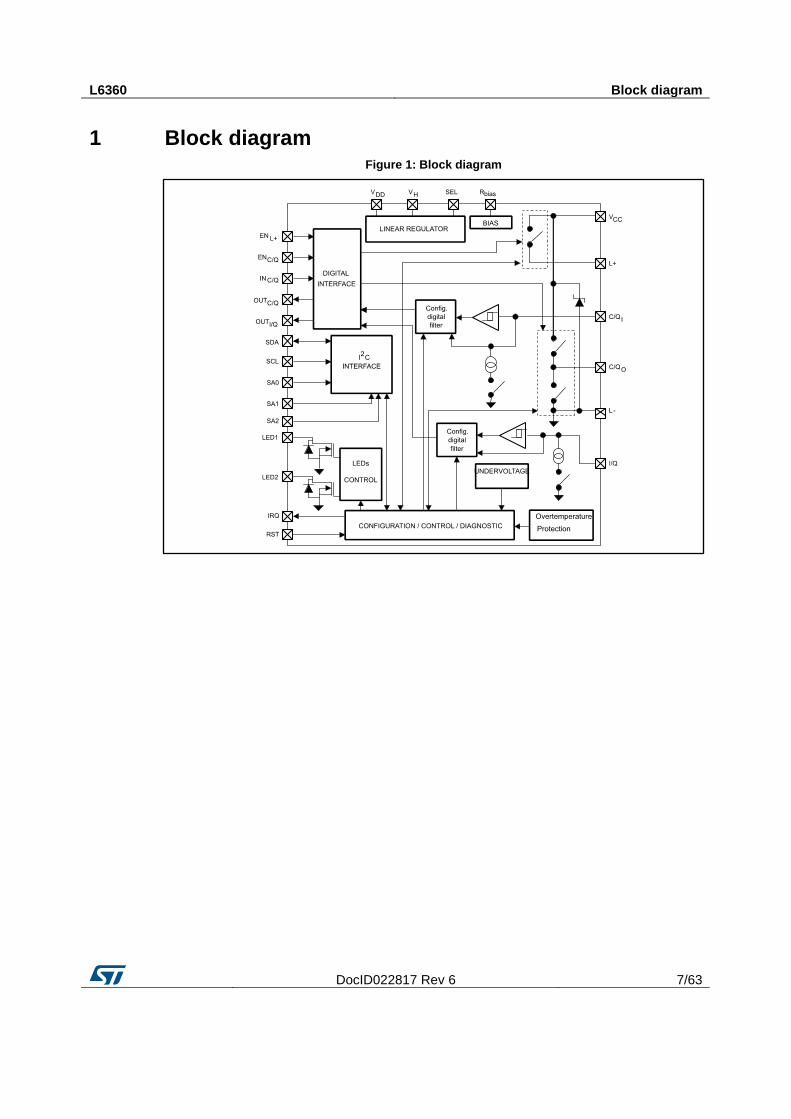
L6360 Block diagram
DocID022817 Rev 6 7/63
1 Block diagram Figure 1: Block diagram
Pin description L6360
8/63 DocID022817 Rev 6
2 Pin description Figure 2: Pin connection (top through view)
Table 1: Pin description
Number Name Function Type
1 VCC IC power supply Supply
2 L- L- line (IC ground) Supply
3 VH Linear regulator supply voltage Supply
4 VDD Linear regulator output voltage Output
5 SA1 Serial address 1 Input
6 SA2 Serial address 2 Input
7 Rbias External resistor for internal reference
generation Input
8 SEL Linear regulator 3.3 V/5 V voltage selection.
Output is 5 V when SEL pin is pulled to GND Input
9 ENC/Q C/Q output enable Input
10 INC/Q C/Q channel logic input Input
11 OUTC/Q C/Q channel logic output Output
12 OUTI/Q I/Q channel logic output Output
13 ENL+ L+ switch enable. When ENL+ is high the switch
is closed Input
14 IRQ Interrupt request signal (open drain) Output
15 SCL Serial clock line Input
16 SDA Serial data line Input/output
17 RST Reset - active low Input
18 SA0 Serial address 0 Input
19 LED1 Status/diagnostic LED (open drain) Output
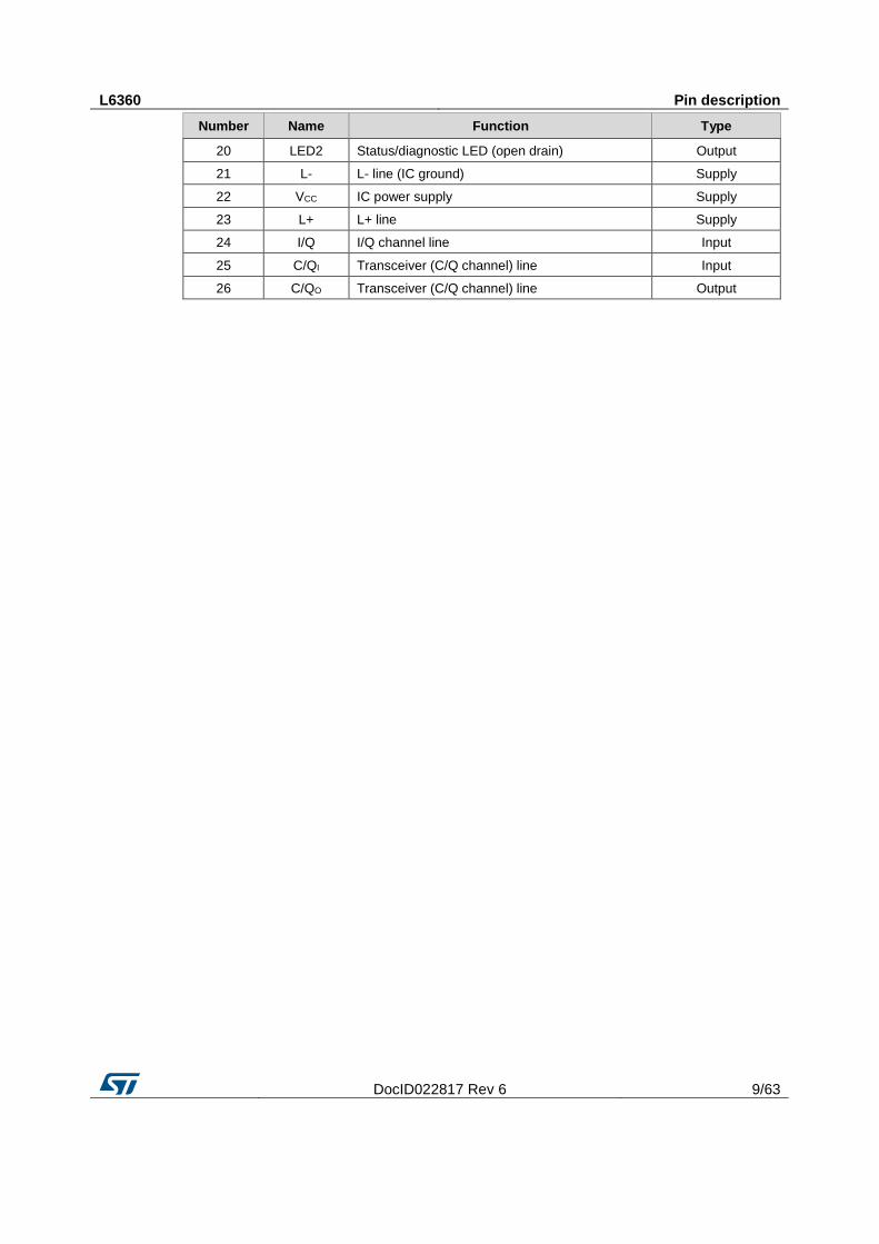
L6360 Pin description
DocID022817 Rev 6 9/63
Number Name Function Type
20 LED2 Status/diagnostic LED (open drain) Output
21 L- L- line (IC ground) Supply
22 VCC IC power supply Supply
23 L+ L+ line Supply
24 I/Q I/Q channel line Input
25 C/QI Transceiver (C/Q channel) line Input
26 C/QO Transceiver (C/Q channel) line Output
Absolute maximum ratings L6360
10/63 DocID022817 Rev 6
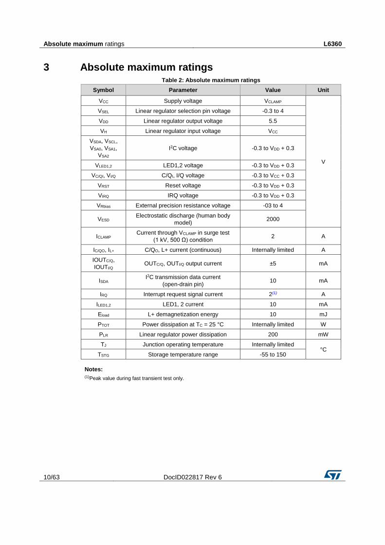
3 Absolute maximum ratings Table 2: Absolute maximum ratings
Symbol Parameter Value Unit
VCC Supply voltage VCLAMP
V
VSEL Linear regulator selection pin voltage -0.3 to 4
VDD Linear regulator output voltage 5.5
VH Linear regulator input voltage VCC
VSDA, VSCL,
VSA0, VSA1,
VSA2
I2C voltage -0.3 to VDD + 0.3
VLED1,2 LED1,2 voltage -0.3 to VDD + 0.3
VC/QI, VI/Q C/QI, I/Q voltage -0.3 to VCC + 0.3
VRST Reset voltage -0.3 to VDD + 0.3
VIRQ IRQ voltage -0.3 to VDD + 0.3
VRbias External precision resistance voltage -03 to 4
VESD Electrostatic discharge (human body
model) 2000
ICLAMP Current through VCLAMP in surge test
(1 kV, 500 Ω) condition 2 A
IC/QO, IL+ C/QO, L+ current (continuous) Internally limited A
IOUTC/Q,
IOUTI/Q OUTC/Q, OUTI/Q output current ±5 mA
ISDA I2C transmission data current
(open-drain pin) 10 mA
IRQ Interrupt request signal current 2(1) A
ILED1,2 LED1, 2 current 10 mA
Eload L+ demagnetization energy 10 mJ
PTOT Power dissipation at TC = 25 °C Internally limited W
PLR Linear regulator power dissipation 200 mW
TJ Junction operating temperature Internally limited °C
TSTG Storage temperature range -55 to 150
Notes:
(1)Peak value during fast transient test only.
L6360 Recommended operating conditions
DocID022817 Rev 6 11/63
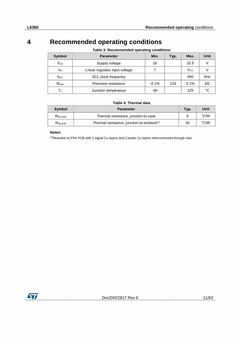
4 Recommended operating conditions Table 3: Recommended operating conditions
Symbol Parameter Min. Typ. Max. Unit
VCC Supply voltage 18
32.5 V
VH Linear regulator input voltage 7
VCC V
fSCL SCL clock frequency
400 kHz
Rbias Precision resistance -0.1% 124 0.1% kΩ
TJ Junction temperature -40
125 °C
Table 4: Thermal data
Symbol Parameter Typ. Unit
Rthj-case Thermal resistance, junction-to-case 6 °C/W
Rthj-amb Thermal resistance, junction-to-ambient(1) 50 °C/W
Notes:
(1)Mounted on FR4 PCB with 2 signal Cu layers and 2 power Cu layers interconnected through vias.
Electrical characteristics L6360
12/63 DocID022817 Rev 6
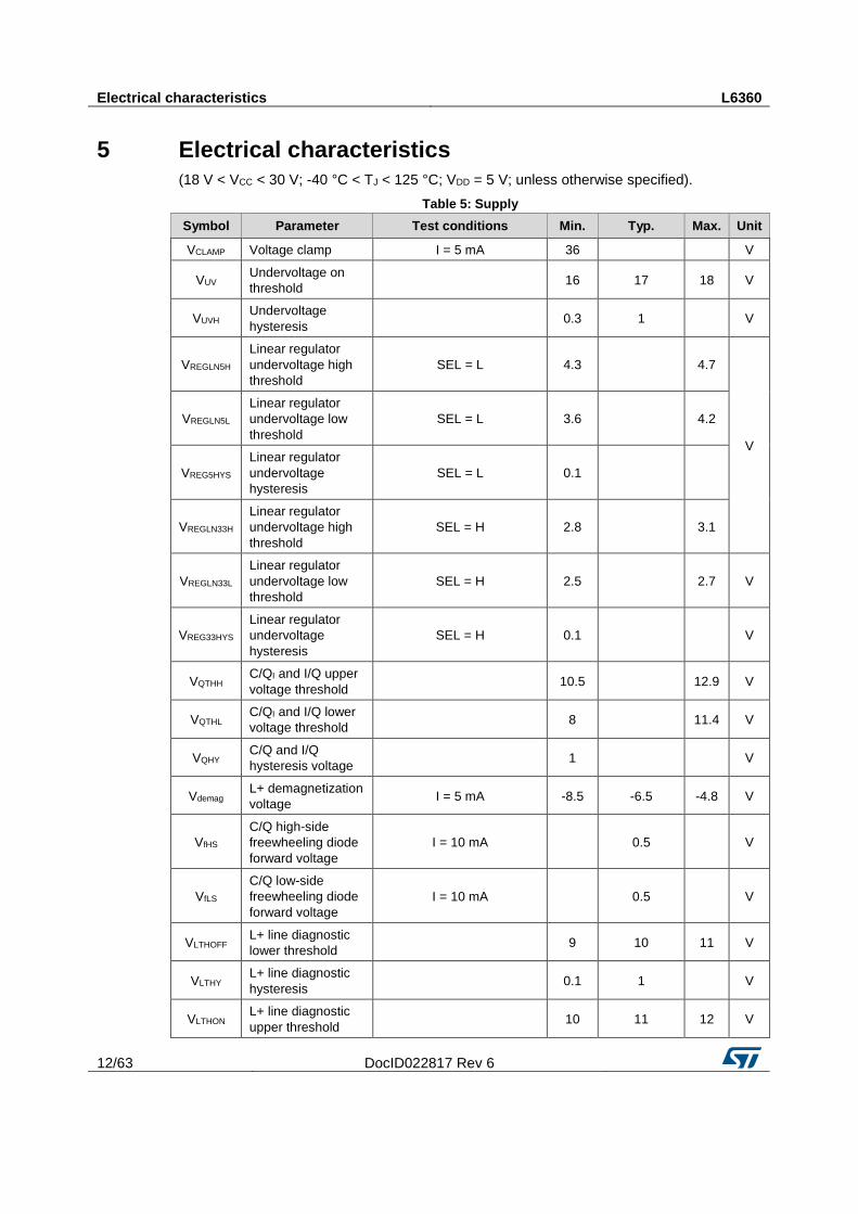
5 Electrical characteristics
(18 V < VCC < 30 V; -40 °C < TJ < 125 °C; VDD = 5 V; unless otherwise specified).
Table 5: Supply
Symbol Parameter Test conditions Min. Typ. Max. Unit
VCLAMP Voltage clamp I = 5 mA 36
V
VUV Undervoltage on
threshold 16 17 18 V
VUVH Undervoltage
hysteresis 0.3 1
V
VREGLN5H
Linear regulator
undervoltage high
threshold
SEL = L 4.3
4.7
V
VREGLN5L
Linear regulator
undervoltage low
threshold
SEL = L 3.6
4.2
VREG5HYS
Linear regulator
undervoltage
hysteresis
SEL = L 0.1
VREGLN33H
Linear regulator
undervoltage high
threshold
SEL = H 2.8
3.1
VREGLN33L
Linear regulator
undervoltage low
threshold
SEL = H 2.5
2.7 V
VREG33HYS
Linear regulator
undervoltage
hysteresis
SEL = H 0.1
V
VQTHH C/QI and I/Q upper
voltage threshold 10.5
12.9 V
VQTHL C/QI and I/Q lower
voltage threshold 8
11.4 V
VQHY C/Q and I/Q
hysteresis voltage 1
V
Vdemag L+ demagnetization
voltage I = 5 mA -8.5 -6.5 -4.8 V
VfHS
C/Q high-side
freewheeling diode
forward voltage
I = 10 mA
0.5
V
VfLS
C/Q low-side
freewheeling diode
forward voltage
I = 10 mA
0.5
V
VLTHOFF L+ line diagnostic
lower threshold 9 10 11 V
VLTHY L+ line diagnostic
hysteresis 0.1 1
V
VLTHON L+ line diagnostic
upper threshold 10 11 12 V
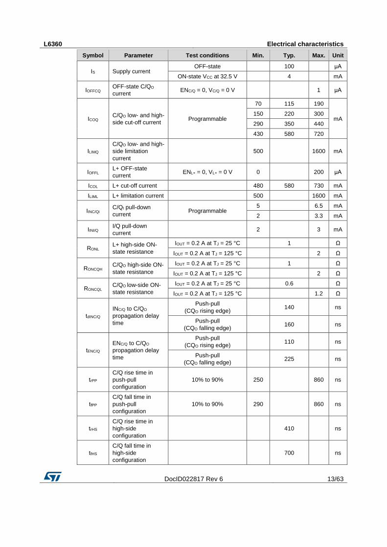
L6360 Electrical characteristics
DocID022817 Rev 6 13/63
Symbol Parameter Test conditions Min. Typ. Max. Unit
IS Supply current OFF-state
100
μA
ON-state VCC at 32.5 V
4
mA
IOFFCQ OFF-state C/QO
current ENC/Q = 0, VC/Q = 0 V
1 μA
ICOQ C/QO low- and high-
side cut-off current Programmable
70 115 190
mA 150 220 300
290 350 440
430 580 720
ILIMQ
C/QO low- and high-
side limitation
current 500
1600 mA
IOFFL L+ OFF-state
current ENL+ = 0, VL+ = 0 V 0
200 μA
ICOL L+ cut-off current
480 580 730 mA
ILIML L+ limitation current
500
1600 mA
IINC/Qi C/QI pull-down
current Programmable
5
6.5 mA
2
3.3 mA
IINI/Q I/Q pull-down
current 2
3 mA
RONL L+ high-side ON-
state resistance
IOUT = 0.2 A at TJ = 25 °C
1
Ω
IOUT = 0.2 A at TJ = 125 °C
2 Ω
RONCQH C/QO high-side ON-
state resistance
IOUT = 0.2 A at TJ = 25 °C
1
Ω
IOUT = 0.2 A at TJ = 125 °C
2 Ω
RONCQL C/QO low-side ON-
state resistance
IOUT = 0.2 A at TJ = 25 °C
0.6
Ω
IOUT = 0.2 A at TJ = 125 °C
1.2 Ω
tdINC/Q
INC/Q to C/QO
propagation delay
time
Push-pull
(CQO rising edge) 140
ns
Push-pull
(CQO falling edge) 160
ns
tENC/Q
ENC/Q to C/QO
propagation delay
time
Push-pull
(CQO rising edge) 110
ns
Push-pull
(CQO falling edge) 225
ns
trPP
C/Q rise time in
push-pull
configuration
10% to 90% 250
860 ns
tfPP
C/Q fall time in
push-pull
configuration
10% to 90% 290
860 ns
trHS
C/Q rise time in
high-side
configuration 410
ns
tfHS
C/Q fall time in
high-side
configuration 700
ns
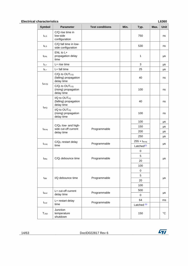
Electrical characteristics L6360
14/63 DocID022817 Rev 6
Symbol Parameter Test conditions Min. Typ. Max. Unit
trLS
C/Q rise time in
low-side
configuration 750
ns
tfLS C/Q fall time in low-
side configuration 530
ns
tENL
ENL to L+
propagation delay
time 1
μs
trL+ L+ rise time
3
μs
tfL+ L+ fall time
25
μs
tdC/Qi
C/QI to OUTC/Q
(falling) propagation
delay time 40
ns
C/QI to OUTC/Q
(rising) propagation
delay time 100
ns
tdI/Q
I/Q to OUTI/Q
(falling) propagation
delay time 40
ns
I/Q to OUTI/Q
(rising) propagation
delay time 100
ns
tdcoq
C/QO low- and high-
side cut-off current
delay time
Programmable
100
μs
150 μs
200 μs
250 μs
trcoq C/QO restart delay
time Programmable
255 × tdcoq
μs
Latched(1)
tdbq C/QI debounce time Programmable
0
μs
5
20
100
tdbl I/Q debounce time Programmable
0
μs
5
20
100
tdcol L+ cut-off current
delay time Programmable
500
μs
0
trcol L+ restart delay
time Programmable
64
ms
Latched (1)
TJSD
Junction
temperature
shutdown 150
°C
L6360 Electrical characteristics
DocID022817 Rev 6 15/63
Symbol Parameter Test conditions Min. Typ. Max. Unit
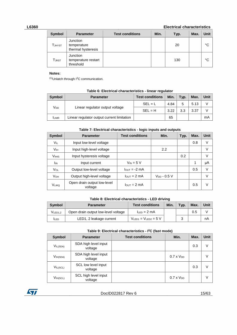
TJHYST
Junction
temperature
thermal hysteresis 20
°C
TJRST
Junction
temperature restart
threshold 130
°C
Notes:
(1)Unlatch through I2C communication.
Table 6: Electrical characteristics - linear regulator
Symbol Parameter Test conditions Min. Typ. Max. Unit
VDD Linear regulator output voltage SEL = L 4.84 5 5.13 V
SEL = H 3.22 3.3 3.37 V
ILIMR Linear regulator output current limitation
65
mA
Table 7: Electrical characteristics - logic inputs and outputs
Symbol Parameter Test conditions Min. Typ. Max. Unit
VIL Input low-level voltage
0.8 V
VIH Input high-level voltage
2.2
V
VIHIS Input hysteresis voltage
0.2
V
IIN Input current VIN = 5 V
1 μA
VOL Output low-level voltage IOUT = -2 mA
0.5 V
VOH Output high-level voltage IOUT = 2 mA VDD - 0.5 V
V
VLIRQ Open drain output low-level
voltage IOUT = 2 mA
0.5 V
Table 8: Electrical characteristics - LED driving
Symbol Parameter Test conditions Min. Typ. Max. Unit
VLED1,2 Open drain output low-level voltage ILED = 2 mA
0.5 V
ILED LED1, 2 leakage current VLED1 = VLED2 = 5 V 3
nA
Table 9: Electrical characteristics - I2C (fast mode)
Symbol Parameter Test conditions Min. Max. Unit
VIL(SDA) SDA high level input
voltage 0.3 V
VIH(SDA) SDA high level input
voltage 0.7 x VDD
V
VIL(SCL) SCL low level input
voltage 0.3 V
VIH(SCL) SCL high level input
voltage 0.7 x VDD
V
Electrical characteristics L6360
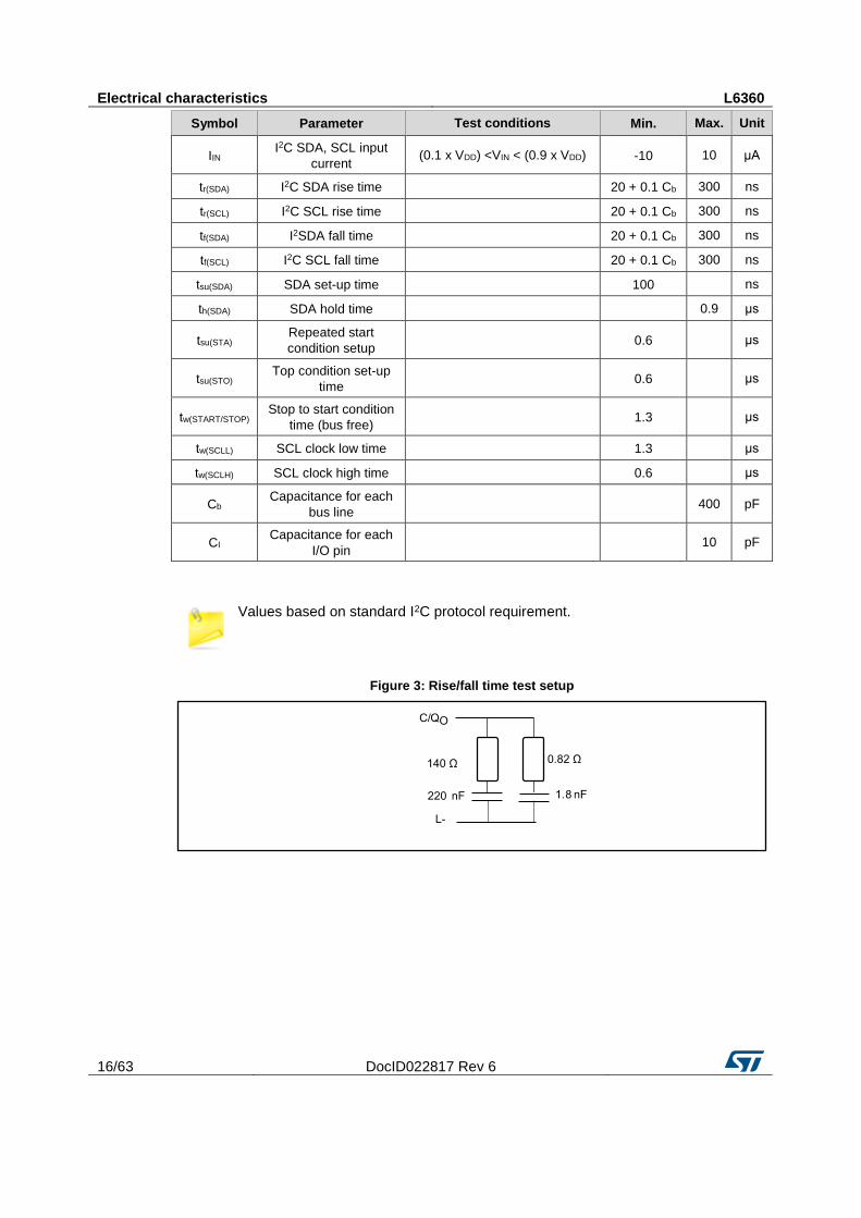
16/63 DocID022817 Rev 6
Symbol Parameter Test conditions Min. Max. Unit
IIN I2C SDA, SCL input
current (0.1 x VDD) <VIN < (0.9 x VDD) -10 10 μA
tr(SDA) I2C SDA rise time
20 + 0.1 Cb 300 ns
tr(SCL) I2C SCL rise time
20 + 0.1 Cb 300 ns
tf(SDA) I2SDA fall time
20 + 0.1 Cb 300 ns
tf(SCL) I2C SCL fall time
20 + 0.1 Cb 300 ns
tsu(SDA) SDA set-up time
100
ns
th(SDA) SDA hold time
0.9 μs
tsu(STA) Repeated start
condition setup 0.6
μs
tsu(STO) Top condition set-up
time 0.6
μs
tw(START/STOP) Stop to start condition
time (bus free) 1.3
μs
tw(SCLL) SCL clock low time
1.3
μs
tw(SCLH) SCL clock high time
0.6
μs
Cb Capacitance for each
bus line 400 pF
CI Capacitance for each
I/O pin 10 pF
Values based on standard I2C protocol requirement.
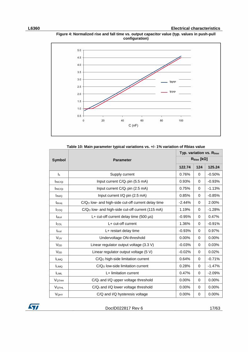
Figure 3: Rise/fall time test setup
L6360 Electrical characteristics
DocID022817 Rev 6 17/63
Figure 4: Normalized rise and fall time vs. output capacitor value (typ. values in push-pull configuration)
Table 10: Main parameter typical variations vs. +/- 1% variation of Rbias value
Symbol Parameter
Typ. variation vs. Rbias
Rbias [kΩ]
122.74 124 125.24
Is Supply current 0.76% 0 -0.50%
IINC/Qi Input current C/QI pin (5.5 mA) 0.93% 0 -0.93%
IINC/Qi Input current C/QI pin (2.5 mA) 0.75% 0 -1.13%
IINI/Q Input current I/Q pin (2.5 mA) 0.85% 0 -0.85%
tdcoq C/QO low- and high-side cut-off current delay time -2.44% 0 2.00%
ICOQ C/QO low- and high-side cut-off current (115 mA) 1.19% 0 -1.28%
tdcol L+ cut-off current delay time (500 µs) -0.95% 0 0.47%
ICOL L+ cut-off current 1.36% 0 -0.91%
trcol L+ restart delay time -0.93% 0 0.97%
VUV Undervoltage ON-threshold 0.00% 0 0.00%
VDD Linear regulator output voltage (3.3 V) -0.03% 0 0.03%
VDD Linear regulator output voltage (5 V) -0.02% 0 0.02%
ILIMQ C/QO high-side limitation current 0.64% 0 -0.71%
ILIMQ C/QO low-side limitation current 0.28% 0 -1.47%
ILIML L+ limitation current 0.47% 0 -2.09%
VQTHH C/QI and I/Q upper voltage threshold 0.00% 0 0.00%
VQTHL C/QI and I/Q lower voltage threshold 0.00% 0 0.00%
VQHY C/Q and I/Q hysteresis voltage 0.00% 0 0.00%
Electrical characteristics L6360
18/63 DocID022817 Rev 6
Symbol Parameter
Typ. variation vs. Rbias
Rbias [kΩ]
122.74 124 125.24
trPP C/Q rise time in push-pull configuration -1.59% 0 1.18%
tfPP C/Q fall time in push-pull configuration -2.14% 0 0.94%
tdINC/Q INC/Q to C/QO propagation delay time (rising) -1.44% 0 0.75%
tdINC/Q INC/Q to C/QO propagation delay time (falling) -2.36% 0 0.18%
tdC/Qi C/QI to OUTC/Q propagation delay time (rising) 0.49% 0 1.13%
tdC/Qi C/QI to OUTC/Q propagation delay time (falling) 1.82% 0 0.03%
tdbq C/QI debounce time (100 µs) -1.76% 0 1.50%
tdcoq C/QO low- and high-side cut-off current delay time (200 µs) -1.27% 0 2.00%
ICOQ C/QO low-side cut-off current (220 mA) 0.39% 0 -1.56%
ICOQ C/QO low-side cut-off current (350 mA) 0.36% 0 -1.43%
ICOQ C/QO low-side cut-off current (580 mA) 0.65% 0 -1.72%
trcoq C/QO restart delay time -0.90% 0 0.97%
ICOQ C/QO high-side cut-off current (220 mA) 0.84% 0 -0.84%
ICOQ C/QO high-side cut-off current (350 mA) 1.38% 0 -0.69%
ICOQ C/QO high-side cut-off current (580 mA) 1.08% 0 -1.08%
L6360 Device configuration
DocID022817 Rev 6 19/63
6 Device configuration
SDA and SCL configure the L6360 device through I2C.
6.1 Introduction
The I2C bus interface serves as an interface between the microcontroller and the serial I2C bus. It provides single master functions, and controls all I2C bus-specific sequencing, protocol and timing. It supports fast I2C mode (400 kHz).
6.2 Main features
Parallel bus/I2C protocol converter
Interrupt generation
Fast I2C mode
7-bit addressing
6.3 General description
In addition to receiving and transmitting data, this interface converts it from serial to parallel format and vice versa. The interface is connected to the I2C bus by a data pin (SDA) and a clock pin (SCL).
6.4 SDA/SCL line control
SDA is a bi-directional line, SCL is the clock input. SDA should be connected to a positive supply voltage via a current-source or pull-up resistor. When the bus is free, both lines are HIGH. The output stages of the devices connected to the bus must have an open drain or open collector output to perform the wired AND function. Data on the I2C bus can be transferred to rates up to 400 Kbit/s in fast mode. The number of interfaces connected to the bus is limited by the bus capacitance. For a single master application, the master's SCL output can be a push-pull driver provided that there are no devices on the bus which would stretch the clock. Transmitter mode: the microcontroller interface holds the clock line low before transmission. Receiver mode: the microcontroller interface holds the clock line low after reception. When the I2C microcontroller cell is enabled, the SDA and SCL ports must be configured as floating inputs. In this case, the value of the external pull-up resistors used depends on the application. When the I2C microcontroller cell is disabled, the SDA and SCL ports revert to being standard I/O port pins. On the L6360, the SDA output is an open drain pin.
6.5 Mode selection
Possible data transfer formats are:
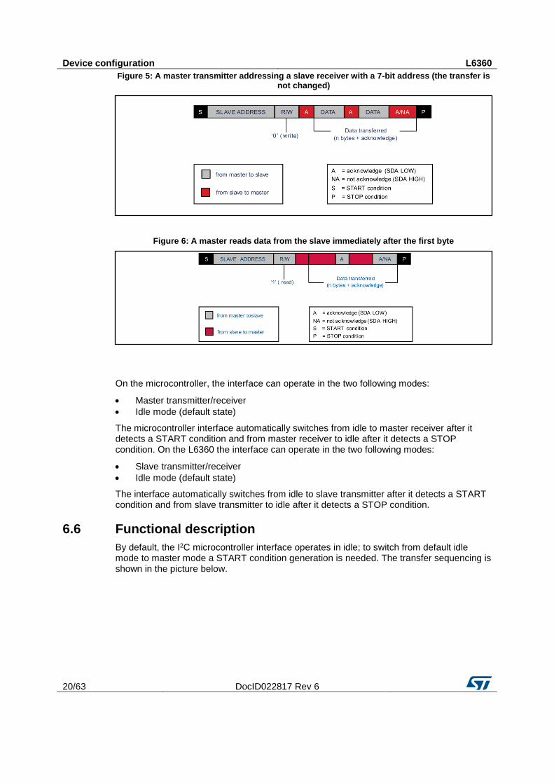
The master transmitter transmits to the slave receiver. The transfer direction is not changed
The slave receiver acknowledges each byte
The master reads data from the slave immediately after the first byte (see Figure 6: "A master reads data from the slave immediately after the first byte"). At the moment of the first acknowledge, the master transmitter becomes a master receiver and the slave receiver becomes a slave transmitter
This first acknowledge is still generated by the slave. Subsequent acknowledges are generated by the master. The STOP condition is generated by the master which sends a not-acknowledge (A) just prior to the STOP condition.
Device configuration L6360
20/63 DocID022817 Rev 6
Figure 5: A master transmitter addressing a slave receiver with a 7-bit address (the transfer is not changed)
Figure 6: A master reads data from the slave immediately after the first byte
On the microcontroller, the interface can operate in the two following modes:
Master transmitter/receiver
Idle mode (default state)
The microcontroller interface automatically switches from idle to master receiver after it detects a START condition and from master receiver to idle after it detects a STOP condition. On the L6360 the interface can operate in the two following modes:
Slave transmitter/receiver
Idle mode (default state)
The interface automatically switches from idle to slave transmitter after it detects a START condition and from slave transmitter to idle after it detects a STOP condition.
6.6 Functional description
By default, the I2C microcontroller interface operates in idle; to switch from default idle mode to master mode a START condition generation is needed. The transfer sequencing is shown in the picture below.
L6360 Device configuration
DocID022817 Rev 6 21/63
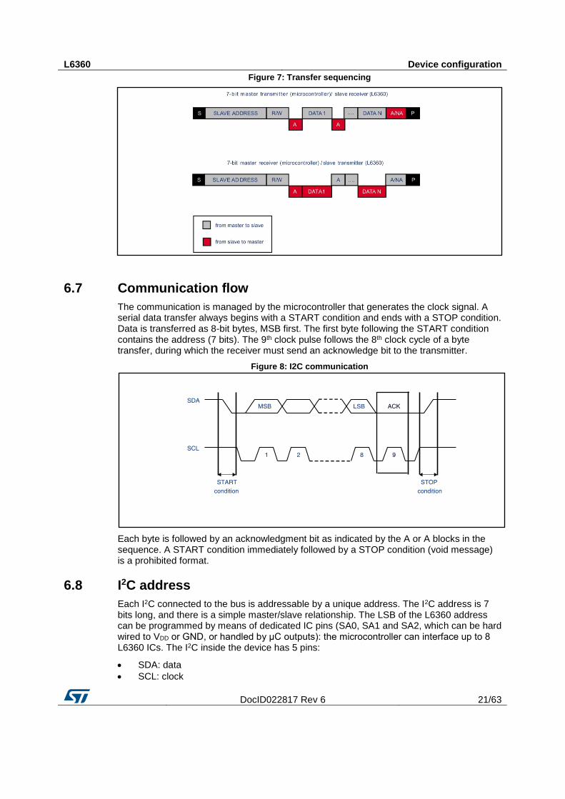
Figure 7: Transfer sequencing
6.7 Communication flow
The communication is managed by the microcontroller that generates the clock signal. A serial data transfer always begins with a START condition and ends with a STOP condition. Data is transferred as 8-bit bytes, MSB first. The first byte following the START condition contains the address (7 bits). The 9th clock pulse follows the 8th clock cycle of a byte transfer, during which the receiver must send an acknowledge bit to the transmitter.
Figure 8: I2C communication
Each byte is followed by an acknowledgment bit as indicated by the A or A blocks in the sequence. A START condition immediately followed by a STOP condition (void message) is a prohibited format.
6.8 I2C address
Each I2C connected to the bus is addressable by a unique address. The I2C address is 7 bits long, and there is a simple master/slave relationship. The LSB of the L6360 address can be programmed by means of dedicated IC pins (SA0, SA1 and SA2, which can be hard wired to VDD or GND, or handled by μC outputs): the microcontroller can interface up to 8 L6360 ICs. The I2C inside the device has 5 pins:
SDA: data
SCL: clock
Device configuration L6360
22/63 DocID022817 Rev 6
SA0: LSB of the L6360 address
SA1: bit 1 of the L6360 address
SA2: bit 2 of the L6360 address
The I2C L6360 IC address is:
Fixed part (4 MSBits): set to “1100”
Programmable part (3 LSBits) by hardware: from “000 to 111" connecting SAx pins to GND or VDD
In the L6360 the SDA is an open drain pin.
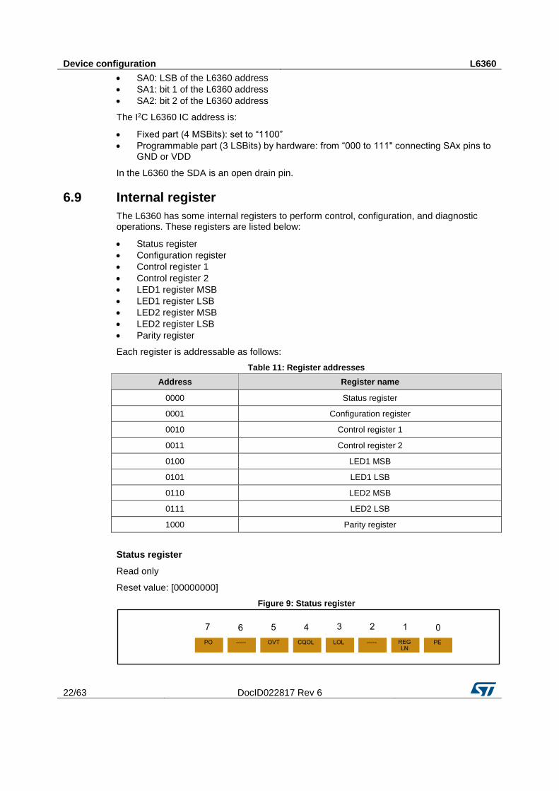
6.9 Internal register
The L6360 has some internal registers to perform control, configuration, and diagnostic operations. These registers are listed below:
Status register
Configuration register
Control register 1
Control register 2
LED1 register MSB
LED1 register LSB
LED2 register MSB
LED2 register LSB
Parity register
Each register is addressable as follows:
Table 11: Register addresses
Address Register name
0000 Status register
0001 Configuration register
0010 Control register 1
0011 Control register 2
0100 LED1 MSB
0101 LED1 LSB
0110 LED2 MSB
0111 LED2 LSB
1000 Parity register
Status register
Read only
Reset value: [00000000]
Figure 9: Status register
L6360 Device configuration
DocID022817 Rev 6 23/63
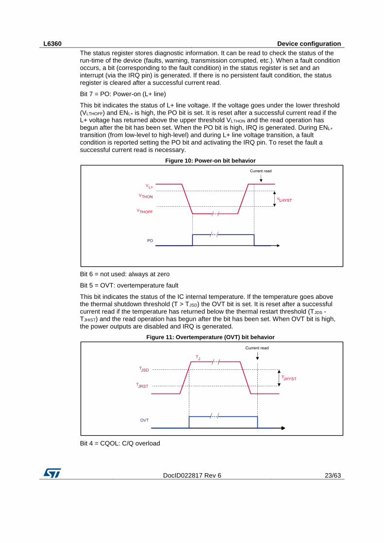
The status register stores diagnostic information. It can be read to check the status of the run-time of the device (faults, warning, transmission corrupted, etc.). When a fault condition occurs, a bit (corresponding to the fault condition) in the status register is set and an interrupt (via the IRQ pin) is generated. If there is no persistent fault condition, the status register is cleared after a successful current read.
Bit 7 = PO: Power-on (L+ line)
This bit indicates the status of L+ line voltage. If the voltage goes under the lower threshold (VLTHOFF) and ENL+ is high, the PO bit is set. It is reset after a successful current read if the L+ voltage has returned above the upper threshold VLTHON and the read operation has begun after the bit has been set. When the PO bit is high, IRQ is generated. During ENL+ transition (from low-level to high-level) and during L+ line voltage transition, a fault condition is reported setting the PO bit and activating the IRQ pin. To reset the fault a successful current read is necessary.
Figure 10: Power-on bit behavior
Bit 6 = not used: always at zero
Bit 5 = OVT: overtemperature fault
This bit indicates the status of the IC internal temperature. If the temperature goes above the thermal shutdown threshold (T > TJSD) the OVT bit is set. It is reset after a successful current read if the temperature has returned below the thermal restart threshold (TJDS - TJHIST) and the read operation has begun after the bit has been set. When OVT bit is high, the power outputs are disabled and IRQ is generated.
Figure 11: Overtemperature (OVT) bit behavior
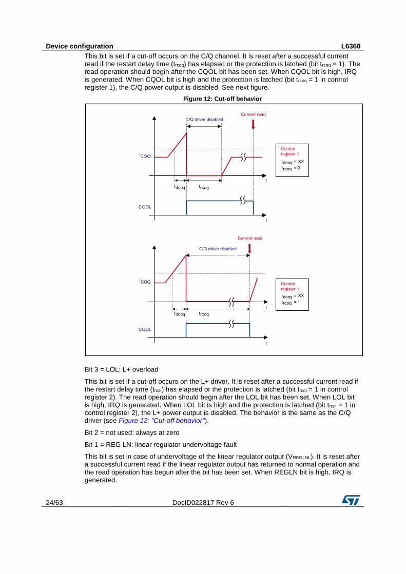
Bit 4 = CQOL: C/Q overload
Device configuration L6360
24/63 DocID022817 Rev 6
This bit is set if a cut-off occurs on the C/Q channel. It is reset after a successful current read if the restart delay time (trcoq) has elapsed or the protection is latched (bit trcoq = 1). The read operation should begin after the CQOL bit has been set. When CQOL bit is high, IRQ is generated. When CQOL bit is high and the protection is latched (bit trcoq = 1 in control register 1), the C/Q power output is disabled. See next figure.
Figure 12: Cut-off behavior
Bit 3 = LOL: L+ overload
This bit is set if a cut-off occurs on the L+ driver. It is reset after a successful current read if the restart delay time (trcol) has elapsed or the protection is latched (bit trcol = 1 in control register 2). The read operation should begin after the LOL bit has been set. When LOL bit is high, IRQ is generated. When LOL bit is high and the protection is latched (bit trcol = 1 in control register 2), the L+ power output is disabled. The behavior is the same as the C/Q driver (see Figure 12: "Cut-off behavior").
Bit 2 = not used: always at zero
Bit 1 = REG LN: linear regulator undervoltage fault
This bit is set in case of undervoltage of the linear regulator output (VREGLNL). It is reset after a successful current read if the linear regulator output has returned to normal operation and the read operation has begun after the bit has been set. When REGLN bit is high, IRQ is generated.
L6360 Device configuration
DocID022817 Rev 6 25/63
Bit 0 = PE: parity check error
This flag is set if parity error occurs.
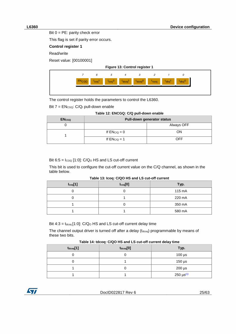
Control register 1
Read/write
Reset value: [00100001]
Figure 13: Control register 1
The control register holds the parameters to control the L6360.
Bit 7 = ENCGQ: C/QI pull-down enable
Table 12: ENCGQ: C/Q pull-down enable
ENCGQ Pull-down generator status
0
Always OFF
1 If ENC/Q = 0 ON
If ENC/Q = 1 OFF
Bit 6:5 = ICOQ [1:0]: C/QO HS and LS cut-off current
This bit is used to configure the cut-off current value on the C/Q channel, as shown in the table below.
Table 13: Icoq: C/QO HS and LS cut-off current
Icoq[1] Icoq[0] Typ.
0 0 115 mA
0 1 220 mA
1 0 350 mA
1 1 580 mA
Bit 4:3 = tdcoq [1:0]: C/QO HS and LS cut-off current delay time
The channel output driver is turned off after a delay (tdcoq) programmable by means of these two bits.
Table 14: tdcoq: C/QO HS and LS cut-off current delay time
tdcoq[1] tdcoq[0] Typ.
0 0 100 µs
0 1 150 µs
1 0 200 µs
1 1 250 µs(1)
Device configuration L6360
26/63 DocID022817 Rev 6
Notes:
(1)According to power dissipation at 2 kHz switching, C < 1 μF and power dissipation 0.7 W.
Bit 2 = trcoq: C/QO restart delay time
After a cut-off event, the channel driver automatically restarts after a delay (trcoq) programmable by means of this bit.
Table 15: trcoq: C/QO restart delay time
trcoq Typ.
0 255x tdcoq
1 Latched(1)
Notes:
(1)Unlatch through I2C communication (reading or writing any internal register).
Bit 1:0 = tdbq [1:0]: C/QI debounce time
Debounce time is the minimum time that data must be in a given state after a transition. It is a programmable time, and can be configured as shown in the table below.
Table 16: tdbq: C/QI debounce time
tdbq[1] tdbq[0] Typ.
0 0 0 µs
0 1 5 µs
1 0 20 µs
1 1 100 µs
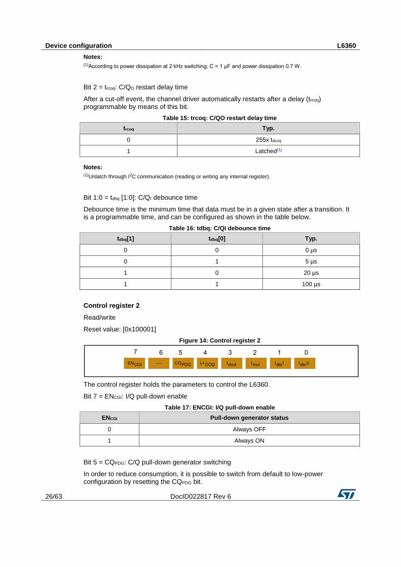
Control register 2
Read/write
Reset value: [0x100001]
Figure 14: Control register 2
The control register holds the parameters to control the L6360.
Bit 7 = ENCGI: I/Q pull-down enable
Table 17: ENCGI: I/Q pull-down enable
ENCGI Pull-down generator status
0 Always OFF
1 Always ON
Bit 5 = CQPDG: C/Q pull-down generator switching
In order to reduce consumption, it is possible to switch from default to low-power configuration by resetting the CQPDG bit.
L6360 Device configuration
DocID022817 Rev 6 27/63
Table 18: CQPDG: C/Q pull-down generator switching
CQPDG Pull-down generator status
0 IINI/Qi (input current C/QI pin) = 2.5 mA
1 IINC/Qi (input current C/QI pin) = 5.5 mA
Bit 4 = L+COD: L+ cut-off disable
The cut-off function on the L+ switch can be enabled or disabled according to the L+COD bit.
Table 19: L+COD: L+ cut-off disable
L+COD L+ cut-off current status
0 Enabled
1 Disabled
As the cut-off function is intended to protect the integrated switches against overload and short-circuit, disabling the cut-off is not recommended.
Bit 3 = tDCOL: L+ cut-off current delay time
The channel output driver is turned off after a delay (tDCOL) programmable by this bit.
Table 20: tDCOL: L+ HS cut-off current delay time
tDCOL Typ.
0 500 µs
1 0 µs
Bit 2 = tRCOL: L+ restart delay
After a cut-off event, the channel driver automatically restarts again after a delay (tRCOL) programmable by this bit.
Table 21: tRCOL: L+ restart delay
tRCOL Typ.
0 64 ms
1 Latched(1)
Notes:
(1)Unlatch through I2C communication (reading or writing any internal register).
Bit 1:0 = tdbi [1:0]: I/Q debounce time
Debounce time is the minimum time that data must be in a given state after a transition. It is a programmable time, and it can be configured as shown in the following table.
Device configuration L6360
28/63 DocID022817 Rev 6
Table 22: Bit 1:0 = tdbi [1:0]: I/Q debounce time
tdbi[1] tdbi[0] Typ.
0 0 0 µs
0 1 5 µs
1 0 20 µs
1 1 100 µs
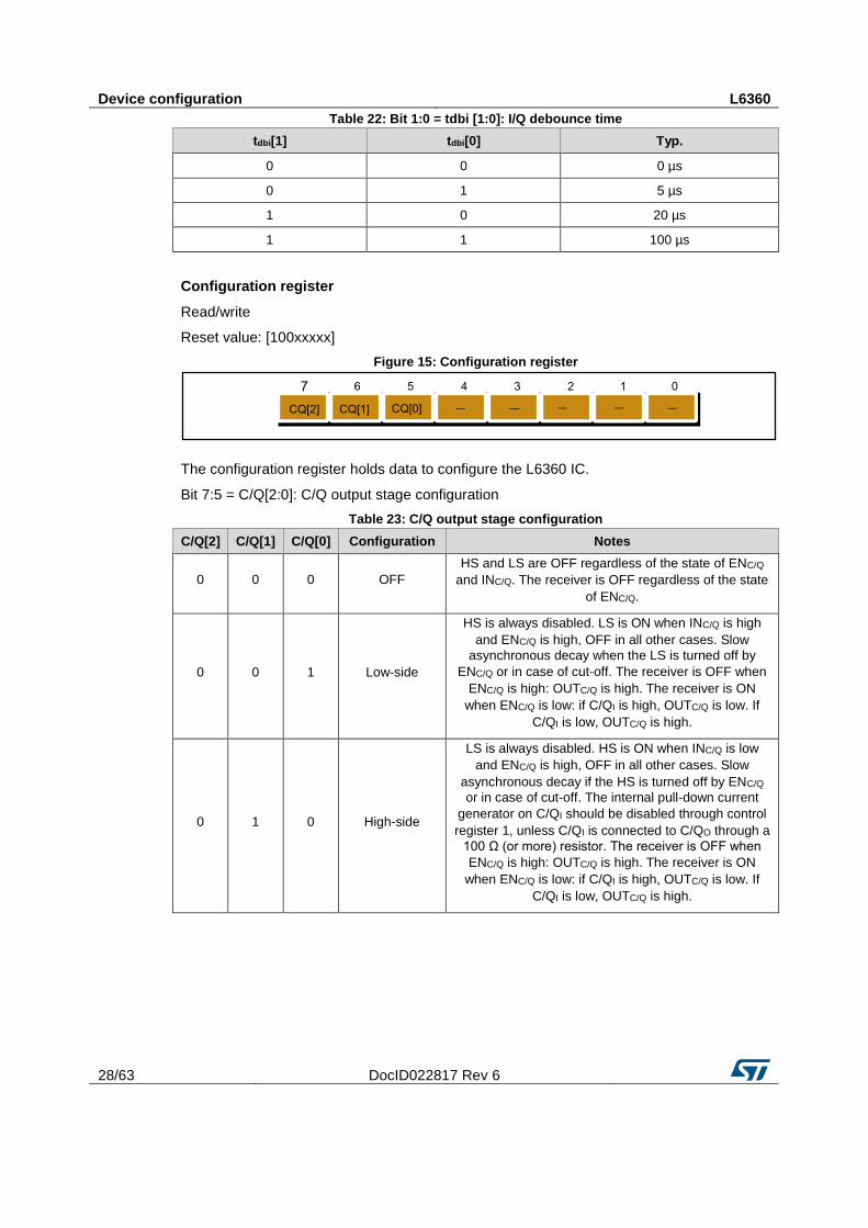
Configuration register
Read/write
Reset value: [100xxxxx]
Figure 15: Configuration register
The configuration register holds data to configure the L6360 IC.
Bit 7:5 = C/Q[2:0]: C/Q output stage configuration
Table 23: C/Q output stage configuration
C/Q[2] C/Q[1] C/Q[0] Configuration Notes
0 0 0 OFF HS and LS are OFF regardless of the state of ENC/Q
and INC/Q. The receiver is OFF regardless of the state
of ENC/Q.
0 0 1 Low-side
HS is always disabled. LS is ON when INC/Q is high
and ENC/Q is high, OFF in all other cases. Slow
asynchronous decay when the LS is turned off by
ENC/Q or in case of cut-off. The receiver is OFF when
ENC/Q is high: OUTC/Q is high. The receiver is ON
when ENC/Q is low: if C/QI is high, OUTC/Q is low. If
C/QI is low, OUTC/Q is high.
0 1 0 High-side
LS is always disabled. HS is ON when INC/Q is low
and ENC/Q is high, OFF in all other cases. Slow
asynchronous decay if the HS is turned off by ENC/Q
or in case of cut-off. The internal pull-down current
generator on C/QI should be disabled through control
register 1, unless C/QI is connected to C/QO through a
100 Ω (or more) resistor. The receiver is OFF when
ENC/Q is high: OUTC/Q is high. The receiver is ON
when ENC/Q is low: if C/QI is high, OUTC/Q is low. If
C/QI is low, OUTC/Q is high.
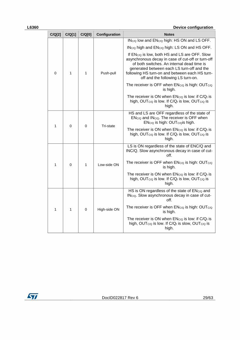
L6360 Device configuration
DocID022817 Rev 6 29/63
C/Q[2] C/Q[1] C/Q[0] Configuration Notes
0 1 1 Push-pull
INC/Q low and ENC/Q high: HS ON and LS OFF.
INC/Q high and ENC/Q high: LS ON and HS OFF.
If ENC/Q is low, both HS and LS are OFF. Slow asynchronous decay in case of cut-off or turn-off
of both switches. An internal dead time is generated between each LS turn-off and the
following HS turn-on and between each HS turn-off and the following LS turn-on.
The receiver is OFF when ENC/Q is high: OUTC/Q is high.
The receiver is ON when ENC/Q is low: if C/QI is high, OUTC/Q is low. If C/QI is low, OUTC/Q is
high.
1 0 0 Tri-state
HS and LS are OFF regardless of the state of ENC/Q and INC/Q. The receiver is OFF when
ENC/Q is high: OUTC/Qis high.
The receiver is ON when ENC/Q is low: if C/QI is high, OUTC/Q is low. If C/QI is low, OUTC/Q is
high.
1 0 1 Low-side ON
LS is ON regardless of the state of ENC/Q and INC/Q. Slow asynchronous decay in case of cut-
off.
The receiver is OFF when ENC/Q is high: OUTC/Q is high.
The receiver is ON when ENC/Q is low: if C/QI is high, OUTC/Q is low. If C/QI is low, OUTC/Q is
high.
1 1 0 High-side ON
HS is ON regardless of the state of ENC/Q and INC/Q. Slow asynchronous decay in case of cut-
off.
The receiver is OFF when ENC/Q is high: OUTC/Q is high.
The receiver is ON when ENC/Q is low: if C/QI is high, OUTC/Q is low. If C/QI is slow, OUTC/Q is
high.
Device configuration L6360
30/63 DocID022817 Rev 6
C/Q[2] C/Q[1] C/Q[0] Configuration Notes
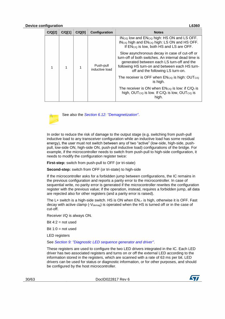
1 1 1 Push-pull
inductive load
INC/Q low and ENC/Q high: HS ON and LS OFF. INC/Q high and ENC/Q high: LS ON and HS OFF.
If ENC/Q is low, both HS and LS are OFF.
Slow asynchronous decay in case of cut-off or turn-off of both switches. An internal dead time is
generated between each LS turn-off and the following HS turn-on and between each HS turn-
off and the following LS turn-on.
The receiver is OFF when ENC/Q is high: OUTC/Q is high.
The receiver is ON when ENC/Q is low: if C/QI is high, OUTC/Q is low. If C/QI is low, OUTC/Q is
high.
See also the Section 6.12: "Demagnetization".
In order to reduce the risk of damage to the output stage (e.g. switching from push-pull inductive load to any transceiver configuration while an inductive load has some residual energy), the user must not switch between any of two “active” (low-side, high-side, push-pull, low-side ON, high-side ON, push-pull inductive load) configurations of the bridge. For example, if the microcontroller needs to switch from push-pull to high-side configuration, it needs to modify the configuration register twice:
First-step: switch from push-pull to OFF (or tri-state)
Second-step: switch from OFF (or tri-state) to high-side
If the microcontroller asks for a forbidden jump between configurations, the IC remains in the previous configuration and reports a parity error to the microcontroller. In case of sequential write, no parity error is generated if the microcontroller rewrites the configuration register with the previous value; if the operation, instead, requires a forbidden jump, all data are rejected also for other registers (and a parity error is raised).
The L+ switch is a high-side switch. HS is ON when ENL+ is high, otherwise it is OFF. Fast decay with active clamp (-Vdemag) is operated when the HS is turned off or in the case of cut-off.
Receiver I/Q is always ON.
Bit 4:2 = not used
Bit 1:0 = not used
LED registers
See Section 9: "Diagnostic LED sequence generator and driver".
These registers are used to configure the two LED drivers integrated in the IC. Each LED driver has two associated registers and turns on or off the external LED according to the information stored in the registers, which are scanned with a rate of 63 ms per bit. LED drivers can be used for status or diagnostic information, or for other purposes, and should be configured by the host microcontroller.
L6360 Device configuration
DocID022817 Rev 6 31/63
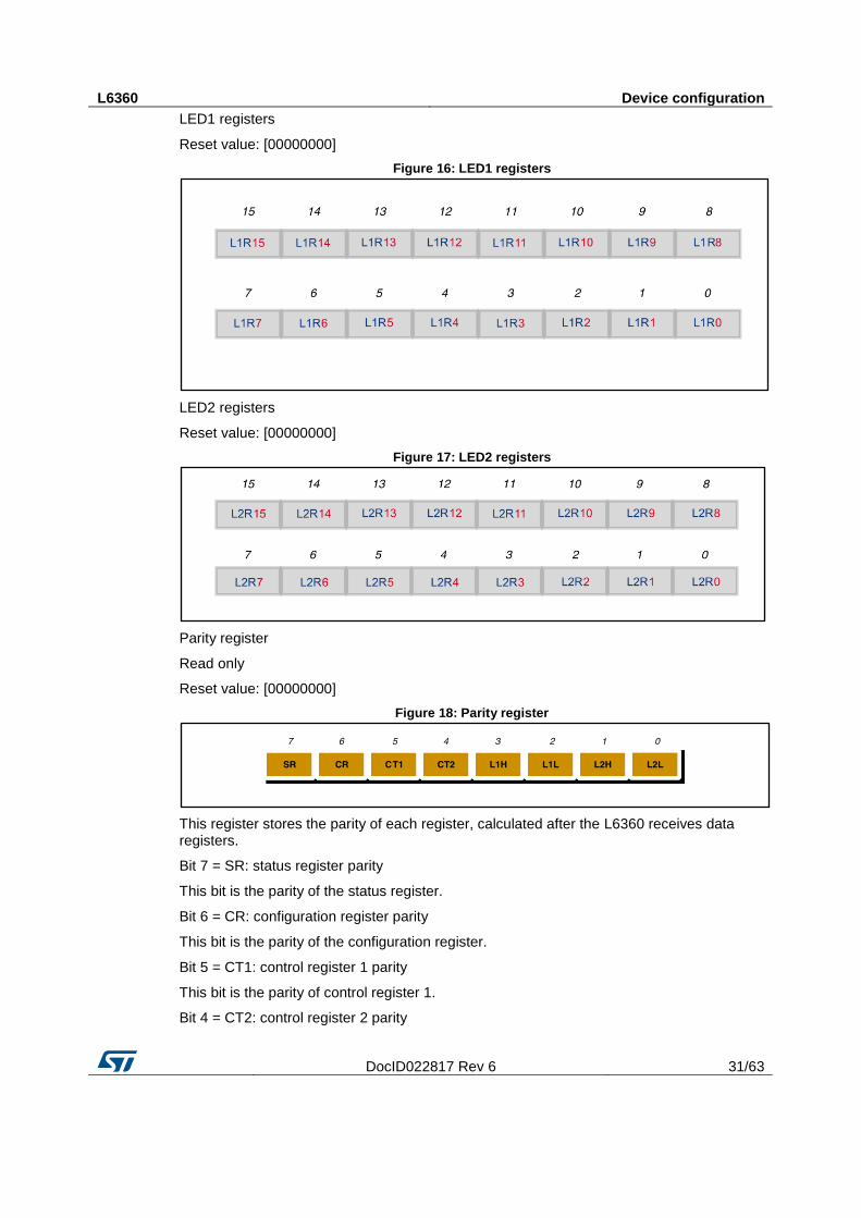
LED1 registers
Reset value: [00000000]
Figure 16: LED1 registers
LED2 registers
Reset value: [00000000]
Figure 17: LED2 registers
Parity register
Read only
Reset value: [00000000]
Figure 18: Parity register
This register stores the parity of each register, calculated after the L6360 receives data registers.
Bit 7 = SR: status register parity
This bit is the parity of the status register.
Bit 6 = CR: configuration register parity
This bit is the parity of the configuration register.
Bit 5 = CT1: control register 1 parity
This bit is the parity of control register 1.
Bit 4 = CT2: control register 2 parity
Device configuration L6360
32/63 DocID022817 Rev 6
This bit is the parity of control register 2.
Bit 3 = L1H: LED1 high register parity
This bit is the parity of the LED1 MSB register (15 down to 8).
Bit 2 = L1L: LED1 low register parity
This bit is the parity of the LED1.
LSB register (7 down to 0).
Bit 1 = L2H: LED2 high register parity
This bit is the parity of the LED2 MSB register (15 down to 8).
Bit 0 = L2L: LED2 low register parity
This bit is the parity of the LED2 LSB register (7 down to 0).
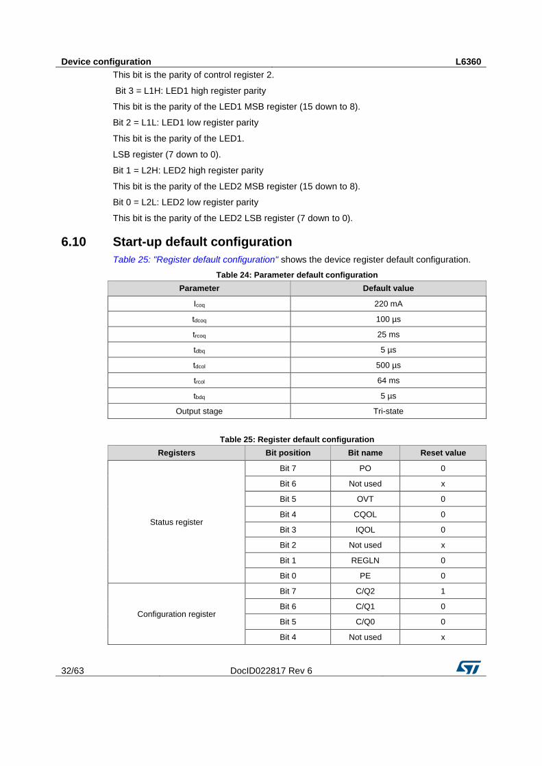
6.10 Start-up default configuration
Table 25: "Register default configuration" shows the device register default configuration.
Table 24: Parameter default configuration
Parameter Default value
Icoq 220 mA
tdcoq 100 µs
trcoq 25 ms
tdbq 5 µs
tdcol 500 µs
trcol 64 ms
tbdq 5 µs
Output stage Tri-state
Table 25: Register default configuration
Registers Bit position Bit name Reset value
Status register
Bit 7 PO 0
Bit 6 Not used x
Bit 5 OVT 0
Bit 4 CQOL 0
Bit 3 IQOL 0
Bit 2 Not used x
Bit 1 REGLN 0
Bit 0 PE 0
Configuration register
Bit 7 C/Q2 1
Bit 6 C/Q1 0
Bit 5 C/Q0 0
Bit 4 Not used x
L6360 Device configuration
DocID022817 Rev 6 33/63
Registers Bit position Bit name Reset value
Bit 3 Not used x
Bit 2 Not used x
Bit 1 Not used x
Bit 0 Not used x
Control register 1
Bit 7 ENCGQ 0
Bit 6 Icoq1 0
Bit 5 Icoq0 1
Bit 4 tdcoq1 0
Bit 3 tdcoq0 0
Bit 2 trcoq 0
Bit 1 tdbq1 0
Bit 0 tdbq0 1
Control register 2
Bit 7 ENCGI 0
Bit 6 Not used x
Bit 5 CQPDG 1
Bit 4 L+COD 0
Bit 3 tdcoi0 0
Bit 2 trcoi 0
Bit 1 tdbi1 0
Bit 0 tdbi0 1
LED1 register MSB
Bit 7 L1R15 0
Bit 6 L1R14 0
Bit 5 L1R13 0
Bit 4 L1R12 0
Bit 3 L1R11 0
Bit 2 L1R10 0
Bit 1 L1R9 0
Bit 0 L1R8 0
LED1 register LSB
Bit 7 L1R7 0
Bit 6 L1R6 0
Bit 5 L1R5 0
Bit 4 L1R4 0
Bit 3 L1R3 0
Bit 2 L1R2 0
Bit 1 L1R1 0
Bit 0 L1R0 0
LED2 register MSB Bit 7 L2R15 0
Device configuration L6360
34/63 DocID022817 Rev 6
Registers Bit position Bit name Reset value
Bit 6 L2R14 0
Bit 5 L2R13 0
Bit 4 L2R12 0
Bit 3 L2R11 0
Bit 2 L2R10 0
Bit 1 L2R9 0
Bit 0 L2R8 0
LED2 register LSB
Bit 7 L2R7 0
Bit 6 L2R6 0
Bit 5 L2R5 0
Bit 4 L2R4 0
Bit 3 L2R3 0
Bit 2 L2R2 0
Bit 1 L2R1 0
Bit 0 L2R0 0
Parity register
Bit 7 SR 0
Bit 6 CR 0
Bit 5 CT1 0
Bit 4 CT2 0
Bit 3 L1H 0
Bit 2 L1L 0
Bit 1 L2H 0
Bit 0 L2L 0
6.11 Interrupt
The IRQ pin (interrupt pin) should normally be held to a high logic level by an external pull-up resistor or microcontroller pin configuration. The internal structure is an open drain transistor. It should be connected directly to the microcontroller so, in the case of a fault event (C/Q overload, power-on L+ line, overtemperature condition, etc.), it is pulled down to a low logic level, reporting the fault condition to the microcontroller.
6.12 Demagnetization
The power stage can be represented as shown in the following figure.
L6360 Device configuration
DocID022817 Rev 6 35/63
Figure 19: Power stage, Q2 is not present on L+ output
When a power stage output (C/Q or L+) is connected to an inductance, the energy stored in the load is:
Equation 1:
E= 1/2 LI2
This energy must be properly dissipated at the switch-off. Without an appropriate circuitry the output voltage would be pulled to very negative values, therefore recovering the stored energy through the breakdown of the power transistor. To avoid this, the output voltage must be clamped so that the voltage across the power switch does not exceed its breakdown voltage. In the case of load connected between the C/QO pin and VCC, at switch-off (of the low-side switch) the output is pushed to a voltage higher than VCC.
6.12.1 Fast demagnetization
It applies to L+ channel only.
Figure 20: Fast demagnetization principle schematic. Load connected to L-
When a high-side driver turns off an inductance, a reversed polarity voltage appears across the load. The output pin (L+) of the power switch becomes more negative than the ground until it reaches the demagnetization voltage, Vdemag. The conduction state of the power switch Q1 is linearly modulated by an internal circuitry in order to keep the voltage at C/Q
Device configuration L6360
36/63 DocID022817 Rev 6
or I/Q pin at about Vdemag until the energy in the load has been dissipated. The energy is dissipated in both IC internal switch and load resistance.
Figure 21: Fast demagnetization waveform. Load connected to L-
6.12.2 Slow demagnetization
It applies to C/Q channel.
Figure 22: Slow demagnetization block. Load connected to L-
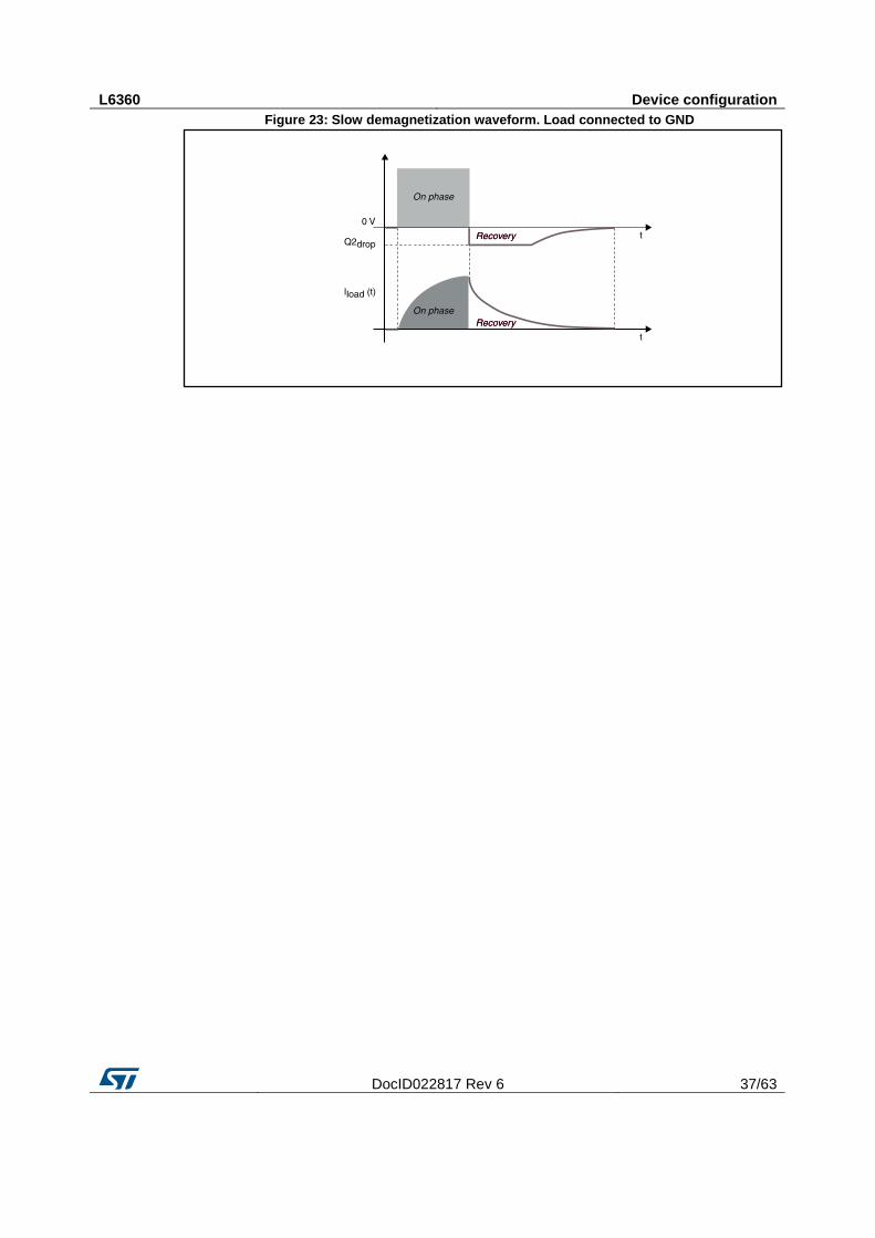
When a high-side driver turns off an inductance a reversed polarity voltage appears across the load. In slow demagnetization configuration the low-side switch Q2 is ON and the C/Q pin is pulled to a voltage slightly (depending on Q2 drop) below the ground (L-). The energy is dissipated in both the IC internal switch and the load resistance. In the case of load connected between the C/Q pin and VCC, at switch-off (of the low-side switch Q2), the switch Q1 is ON and the output is pushed to a voltage slightly higher than VCC.
L6360 Device configuration
DocID022817 Rev 6 37/63
Figure 23: Slow demagnetization waveform. Load connected to GND
I2C protocol L6360
38/63 DocID022817 Rev 6
7 I2C protocol
7.1 Protocol configuration
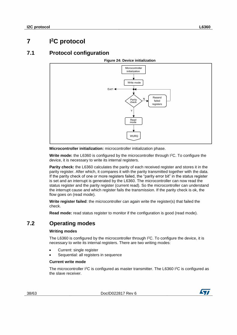
Figure 24: Device initialization
Microcontroller initialization: microcontroller initialization phase.
Write mode: the L6360 is configured by the microcontroller through I2C. To configure the device, it is necessary to write its internal registers.
Parity check: the L6360 calculates the parity of each received register and stores it in the parity register. After which, it compares it with the parity transmitted together with the data. If the parity check of one or more registers failed, the “parity error bit” in the status register is set and an interrupt is generated by the L6360. The microcontroller can now read the status register and the parity register (current read). So the microcontroller can understand the interrupt cause and which register fails the transmission. If the parity check is ok, the flow goes on (read mode).
Write register failed: the microcontroller can again write the register(s) that failed the check.
Read mode: read status register to monitor if the configuration is good (read mode).
7.2 Operating modes
Writing modes
The L6360 is configured by the microcontroller through I2C. To configure the device, it is necessary to write its internal registers. There are two writing modes:
Current: single register
Sequential: all registers in sequence
Current write mode
The microcontroller I2C is configured as master transmitter. The L6360 I2C is configured as the slave receiver.
L6360 I2C protocol
DocID022817 Rev 6 39/63
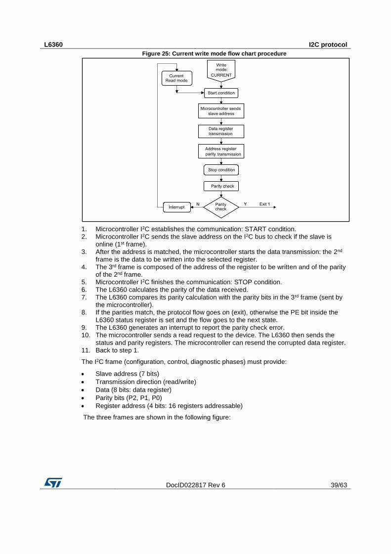
Figure 25: Current write mode flow chart procedure
1. Microcontroller I2C establishes the communication: START condition. 2. Microcontroller I2C sends the slave address on the I2C bus to check if the slave is
online (1st frame). 3. After the address is matched, the microcontroller starts the data transmission: the 2nd
frame is the data to be written into the selected register. 4. The 3rd frame is composed of the address of the register to be written and of the parity
of the 2nd frame. 5. Microcontroller I2C finishes the communication: STOP condition. 6. The L6360 calculates the parity of the data received. 7. The L6360 compares its parity calculation with the parity bits in the 3rd frame (sent by
the microcontroller). 8. If the parities match, the protocol flow goes on (exit), otherwise the PE bit inside the
L6360 status register is set and the flow goes to the next state. 9. The L6360 generates an interrupt to report the parity check error. 10. The microcontroller sends a read request to the device. The L6360 then sends the
status and parity registers. The microcontroller can resend the corrupted data register. 11. Back to step 1.
The I2C frame (configuration, control, diagnostic phases) must provide:
Slave address (7 bits)
Transmission direction (read/write)
Data (8 bits: data register)
Parity bits (P2, P1, P0)
Register address (4 bits: 16 registers addressable)
The three frames are shown in the following figure:
I2C protocol L6360
40/63 DocID022817 Rev 6
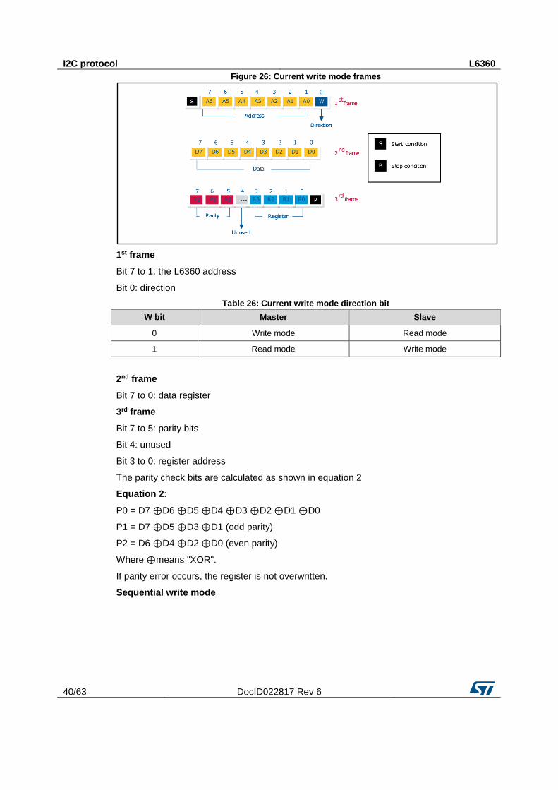
Figure 26: Current write mode frames
1st frame
Bit 7 to 1: the L6360 address
Bit 0: direction
Table 26: Current write mode direction bit
W bit Master Slave
0 Write mode Read mode
1 Read mode Write mode
2nd frame
Bit 7 to 0: data register
3rd frame
Bit 7 to 5: parity bits
Bit 4: unused
Bit 3 to 0: register address
The parity check bits are calculated as shown in equation 2
Equation 2:
P0 = D7 ⊕ D6 ⊕ D5 ⊕ D4 ⊕ D3 ⊕ D2 ⊕ D1 ⊕ D0
P1 = D7 ⊕ D5 ⊕ D3 ⊕ D1 (odd parity)
P2 = D6 ⊕ D4 ⊕ D2 ⊕ D0 (even parity)
Where ⊕ means "XOR".
If parity error occurs, the register is not overwritten.
Sequential write mode
L6360 I2C protocol
DocID022817 Rev 6 41/63
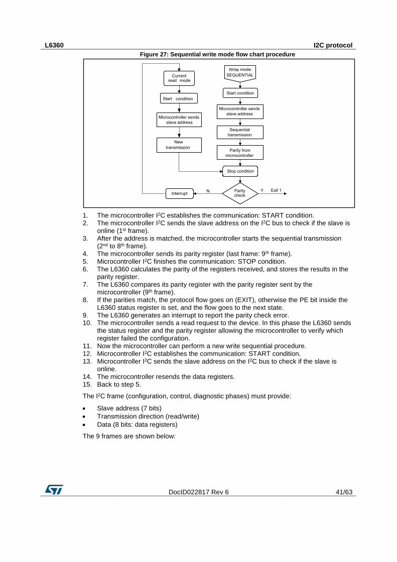
Figure 27: Sequential write mode flow chart procedure
1. The microcontroller I2C establishes the communication: START condition. 2. The microcontroller I2C sends the slave address on the I2C bus to check if the slave is
online (1st frame). 3. After the address is matched, the microcontroller starts the sequential transmission
(2nd to 8th frame). 4. The microcontroller sends its parity register (last frame: 9th frame). 5. Microcontroller I2C finishes the communication: STOP condition. 6. The L6360 calculates the parity of the registers received, and stores the results in the
parity register. 7. The L6360 compares its parity register with the parity register sent by the
microcontroller (9th frame). 8. If the parities match, the protocol flow goes on (EXIT), otherwise the PE bit inside the
L6360 status register is set, and the flow goes to the next state. 9. The L6360 generates an interrupt to report the parity check error. 10. The microcontroller sends a read request to the device. In this phase the L6360 sends
the status register and the parity register allowing the microcontroller to verify which register failed the configuration.
11. Now the microcontroller can perform a new write sequential procedure. 12. Microcontroller I2C establishes the communication: START condition. 13. Microcontroller I2C sends the slave address on the I2C bus to check if the slave is
online. 14. The microcontroller resends the data registers. 15. Back to step 5.
The I2C frame (configuration, control, diagnostic phases) must provide:
Slave address (7 bits)
Transmission direction (read/write)
Data (8 bits: data registers)
The 9 frames are shown below:
I2C protocol L6360
42/63 DocID022817 Rev 6
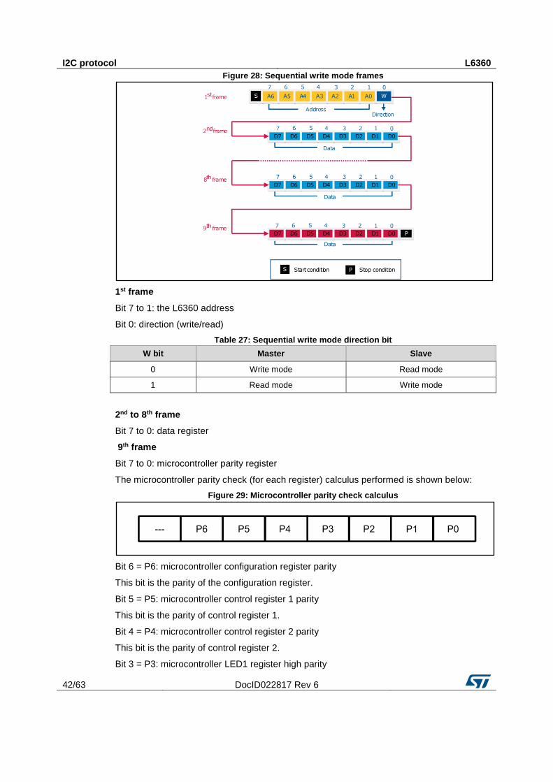
Figure 28: Sequential write mode frames
1st frame
Bit 7 to 1: the L6360 address
Bit 0: direction (write/read)
Table 27: Sequential write mode direction bit
W bit Master Slave
0 Write mode Read mode
1 Read mode Write mode
2nd to 8th frame
Bit 7 to 0: data register
9th frame
Bit 7 to 0: microcontroller parity register
The microcontroller parity check (for each register) calculus performed is shown below:
Figure 29: Microcontroller parity check calculus
Bit 6 = P6: microcontroller configuration register parity
This bit is the parity of the configuration register.
Bit 5 = P5: microcontroller control register 1 parity
This bit is the parity of control register 1.
Bit 4 = P4: microcontroller control register 2 parity
This bit is the parity of control register 2.
Bit 3 = P3: microcontroller LED1 register high parity
L6360 I2C protocol
DocID022817 Rev 6 43/63
This bit is the parity of the LED1 MSB register (15 down to 8).
Bit 2 = P2: microcontroller LED1 register low parity
This bit is the parity of the LED1 LSB register (7 down to 0).
Bit 1 = P1: microcontroller LED2 register high parity
This bit is the parity of the LED2 MSB register high (15 down to 8).
Bit 0 = P0: microcontroller LED2 register low parity
This bit is the parity of the LED2 LSB register high (7 down to 0).
For each register, a parity check is calculated as shown in equation 3
Equation 3:
PX = D7 ⊕ D6 ⊕ D5 ⊕ D4 ⊕ D3 ⊕ D2 ⊕ D1⊕ D0 (X = 0 to 6)
D7 to D0 indicates bits inside each register.
Where ⊕ means "XOR".
If parity error occurs, the registers are not overwritten.
In this writing mode, all writable registers and the microcontroller parity register are sent.
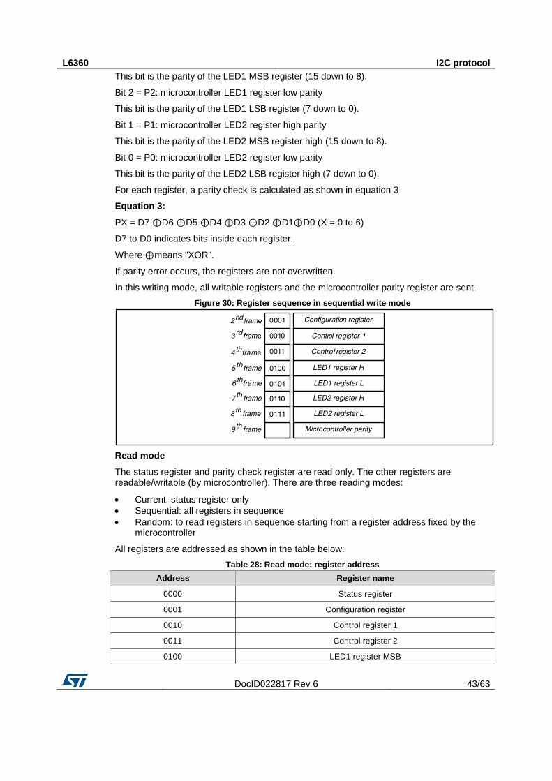
Figure 30: Register sequence in sequential write mode
Read mode
The status register and parity check register are read only. The other registers are readable/writable (by microcontroller). There are three reading modes:
Current: status register only
Sequential: all registers in sequence
Random: to read registers in sequence starting from a register address fixed by the microcontroller
All registers are addressed as shown in the table below:
Table 28: Read mode: register address
Address Register name
0000 Status register
0001 Configuration register
0010 Control register 1
0011 Control register 2
0100 LED1 register MSB
I2C protocol L6360
44/63 DocID022817 Rev 6
Address Register name
0101 LED1 register LSB
0110 LED2 register MSB
0111 LED2 register LSB
1000 Parity register
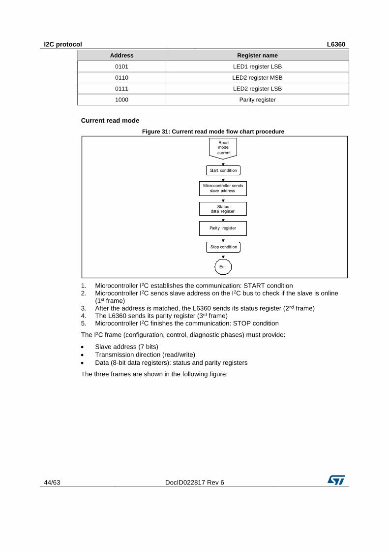
Current read mode
Figure 31: Current read mode flow chart procedure
1. Microcontroller I2C establishes the communication: START condition 2. Microcontroller I2C sends slave address on the I2C bus to check if the slave is online
(1st frame) 3. After the address is matched, the L6360 sends its status register (2nd frame) 4. The L6360 sends its parity register (3rd frame) 5. Microcontroller I2C finishes the communication: STOP condition
The I2C frame (configuration, control, diagnostic phases) must provide:
Slave address (7 bits)
Transmission direction (read/write)
Data (8-bit data registers): status and parity registers
The three frames are shown in the following figure:
L6360 I2C protocol
DocID022817 Rev 6 45/63
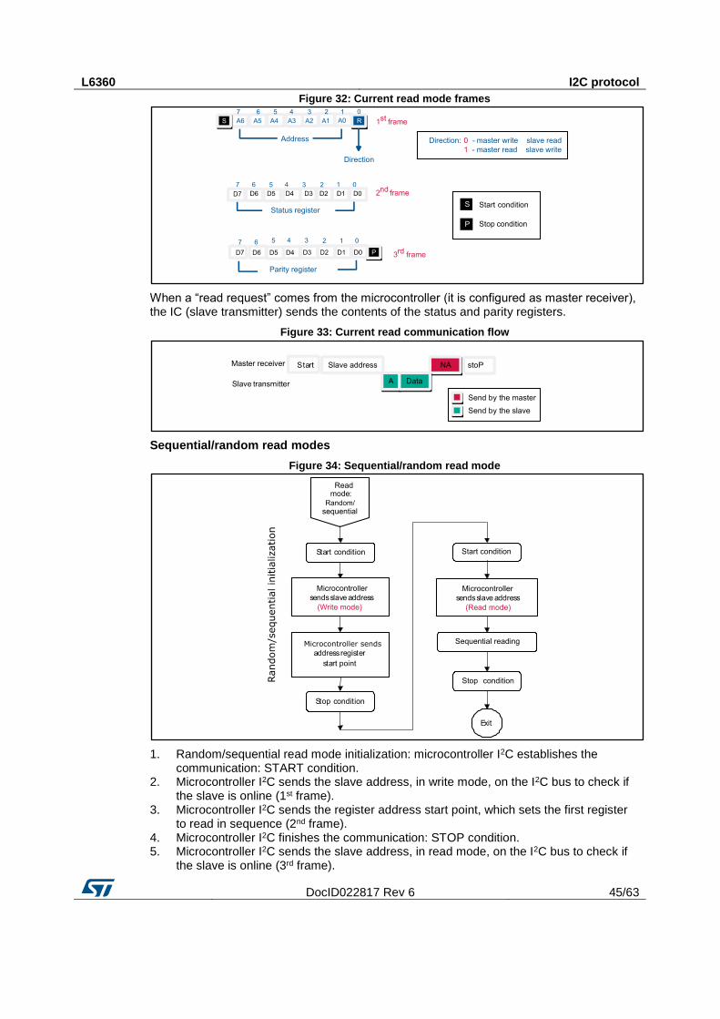
Figure 32: Current read mode frames
When a “read request” comes from the microcontroller (it is configured as master receiver), the IC (slave transmitter) sends the contents of the status and parity registers.
Figure 33: Current read communication flow
Sequential/random read modes
Figure 34: Sequential/random read mode
1. Random/sequential read mode initialization: microcontroller I2C establishes the communication: START condition.
2. Microcontroller I2C sends the slave address, in write mode, on the I2C bus to check if the slave is online (1st frame).
3. Microcontroller I2C sends the register address start point, which sets the first register to read in sequence (2nd frame).
4. Microcontroller I2C finishes the communication: STOP condition. 5. Microcontroller I2C sends the slave address, in read mode, on the I2C bus to check if
the slave is online (3rd frame).
I2C protocol L6360
46/63 DocID022817 Rev 6
6. After the address is matched, the L6360 sends its registers in sequential mode, starting from the register set in the 2nd frame.
7. The microcontroller I2C finishes the communication: STOP condition.
The I2C frame (configuration, control, diagnostic phases) must provide
Slave address (7 bits)
Transmission direction (read/write)
Data (8-bit data register)
The frame structure is shown in the figure below
Figure 35: Sequential/random read communication flow
1st frame
Bit 7 to 1: the L6360 address
Bit 0: direction (write)
2nd frame
Bit 7 to 0: address register starting point
Table 29: Address register
Address Register name
0000 Status register
0001 Configuration register
0010 Control register 1
L6360 I2C protocol
DocID022817 Rev 6 47/63
Address Register name
0011 Control register 2
0100 LED1 register MSB
0101 LED1 register LSB
0110 LED2 register MSB
0111 LED2 register LSB
1000 Parity register
3rd frame
Bit 7 to 1: L6360 address
Bit 0: direction (read)
4th to nth frame
Bit 7 to 0: data register (from address register starting point to penultimate address register)
9th frame
Bit 7 to 0: parity register (the last register)
Physical layer communication L6360
48/63 DocID022817 Rev 6
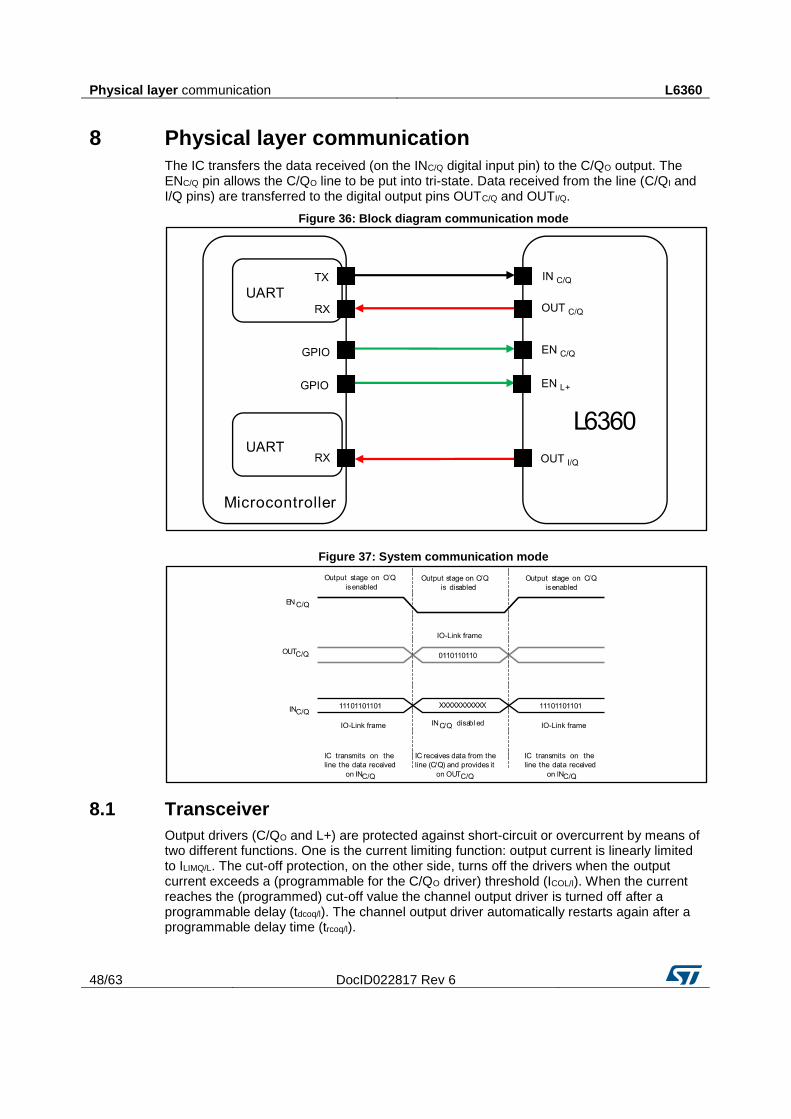
8 Physical layer communication
The IC transfers the data received (on the INC/Q digital input pin) to the C/QO output. The ENC/Q pin allows the C/QO line to be put into tri-state. Data received from the line (C/QI and I/Q pins) are transferred to the digital output pins OUTC/Q and OUTI/Q.
Figure 36: Block diagram communication mode
Figure 37: System communication mode
8.1 Transceiver
Output drivers (C/QO and L+) are protected against short-circuit or overcurrent by means of two different functions. One is the current limiting function: output current is linearly limited to ILIMQ/L. The cut-off protection, on the other side, turns off the drivers when the output current exceeds a (programmable for the C/QO driver) threshold (ICOL/I). When the current reaches the (programmed) cut-off value the channel output driver is turned off after a programmable delay (tdcoq/l). The channel output driver automatically restarts again after a programmable delay time (trcoq/l).
L6360 Physical layer communication
DocID022817 Rev 6 49/63
Figure 38: C/Q or L+ channel cut-off protection
Figure 39: C/Q or L+ channel current limitation and cut-off protection with latched restart
8.2 IEC 61131-2 type 1 digital inputs
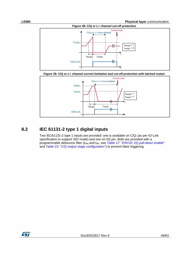
Two IEC61131-2 type 1 inputs are provided: one is available on C/QI (as per IO-Link specification to support SIO mode) and one on I/Q pin. Both are provided with a programmable debounce filter (tdbq and tdbi, see Table 17: "ENCGI: I/Q pull-down enable" and Table 23: "C/Q output stage configuration") to prevent false triggering.
Diagnostic LED sequence generator and driver L6360
50/63 DocID022817 Rev 6
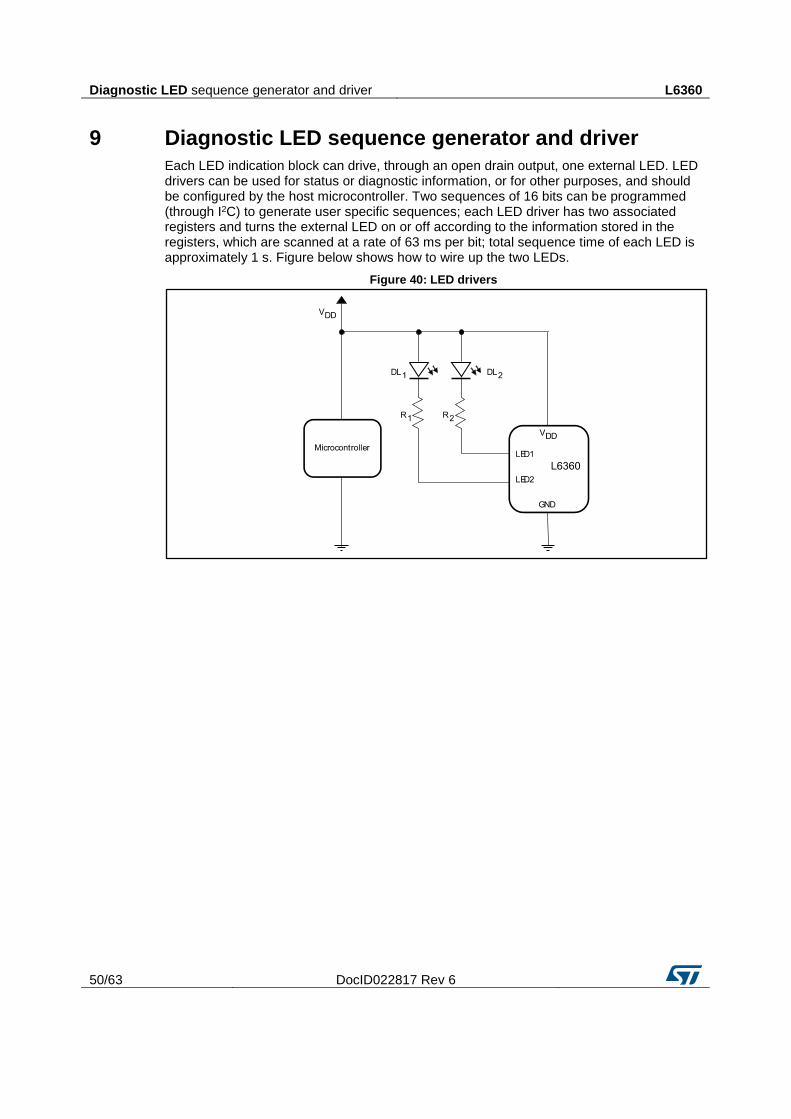
9 Diagnostic LED sequence generator and driver
Each LED indication block can drive, through an open drain output, one external LED. LED drivers can be used for status or diagnostic information, or for other purposes, and should be configured by the host microcontroller. Two sequences of 16 bits can be programmed (through I2C) to generate user specific sequences; each LED driver has two associated registers and turns the external LED on or off according to the information stored in the registers, which are scanned at a rate of 63 ms per bit; total sequence time of each LED is approximately 1 s. Figure below shows how to wire up the two LEDs.
Figure 40: LED drivers
L6360 Line regulator
DocID022817 Rev 6 51/63
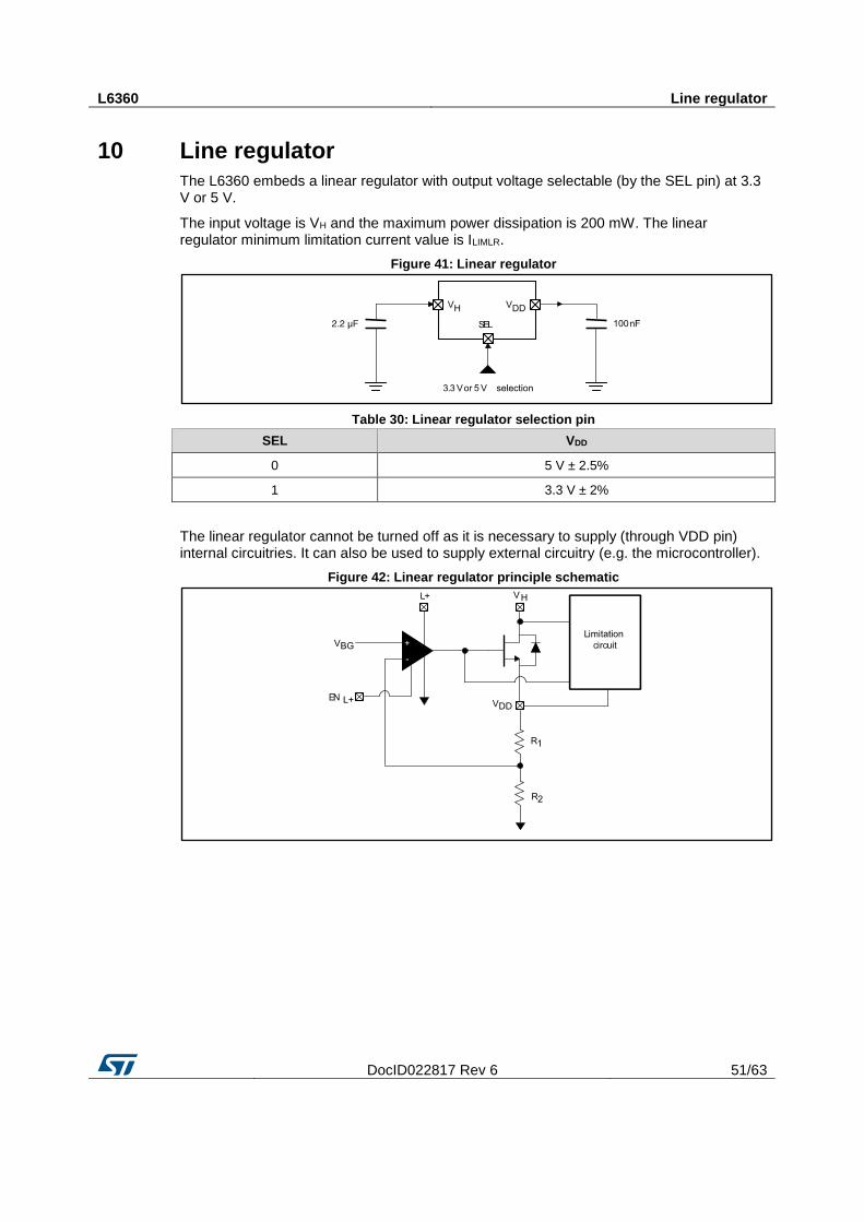
10 Line regulator
The L6360 embeds a linear regulator with output voltage selectable (by the SEL pin) at 3.3 V or 5 V.
The input voltage is VH and the maximum power dissipation is 200 mW. The linear regulator minimum limitation current value is ILIMLR.
Figure 41: Linear regulator
Table 30: Linear regulator selection pin
SEL VDD
0 5 V ± 2.5%
1 3.3 V ± 2%
The linear regulator cannot be turned off as it is necessary to supply (through VDD pin) internal circuitries. It can also be used to supply external circuitry (e.g. the microcontroller).
Figure 42: Linear regulator principle schematic
Application examples L6360
52/63 DocID022817 Rev 6
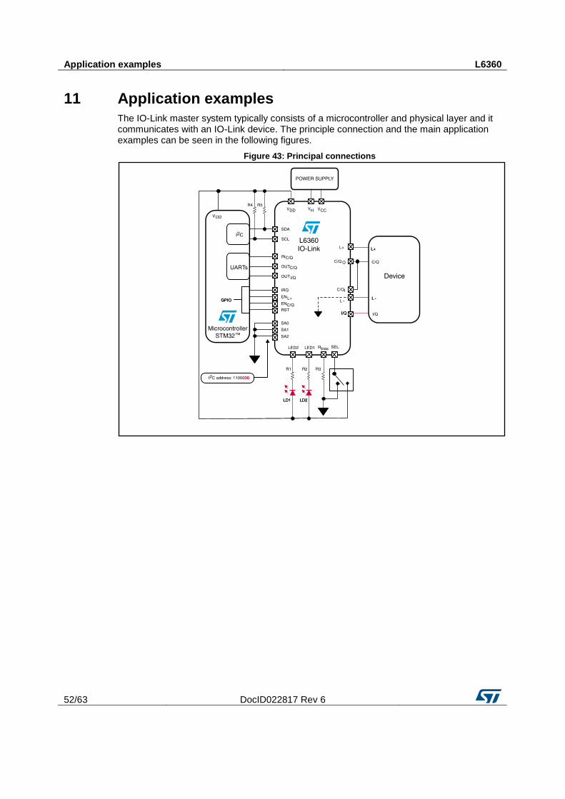
11 Application examples
The IO-Link master system typically consists of a microcontroller and physical layer and it communicates with an IO-Link device. The principle connection and the main application examples can be seen in the following figures.
Figure 43: Principal connections
L6360 Application examples
DocID022817 Rev 6 53/63
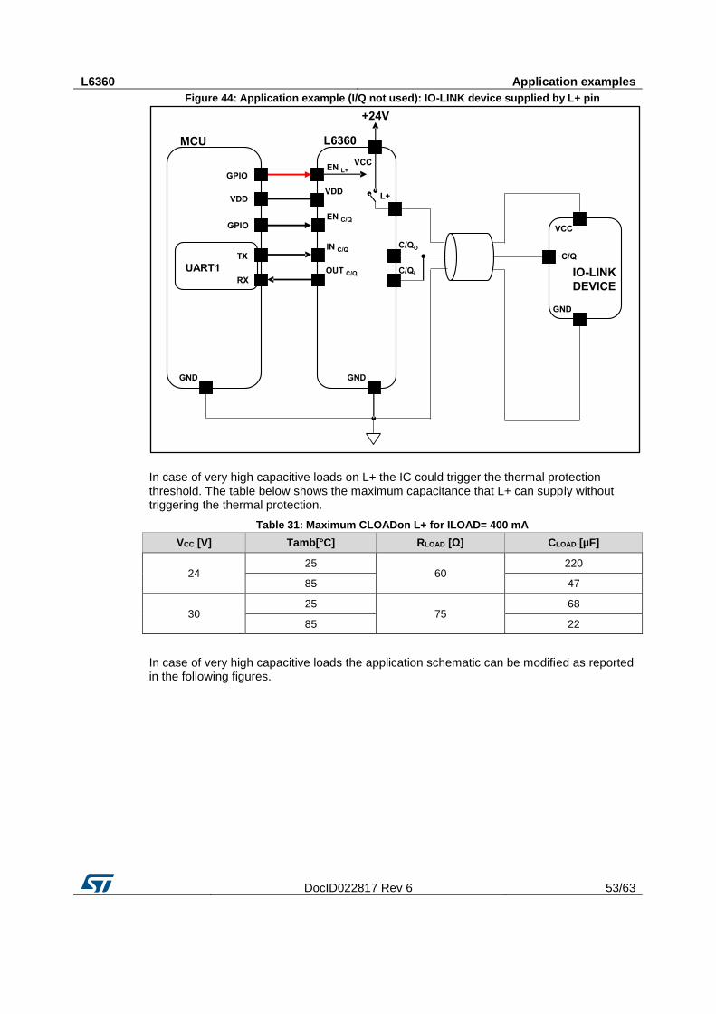
Figure 44: Application example (I/Q not used): IO-LINK device supplied by L+ pin
In case of very high capacitive loads on L+ the IC could trigger the thermal protection threshold. The table below shows the maximum capacitance that L+ can supply without triggering the thermal protection.
Table 31: Maximum CLOADon L+ for ILOAD= 400 mA
VCC [V] Tamb[°C] RLOAD [Ω] CLOAD [µF]
24 25
60 220
85 47
30 25
75 68
85 22
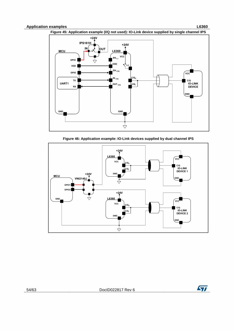
In case of very high capacitive loads the application schematic can be modified as reported in the following figures.
Application examples L6360
54/63 DocID022817 Rev 6
Figure 45: Application example (I/Q not used): IO-Link device supplied by single channel IPS
Figure 46: Application example: IO-Link devices supplied by dual channel IPS
L6360 EMC protection considerations
DocID022817 Rev 6 55/63
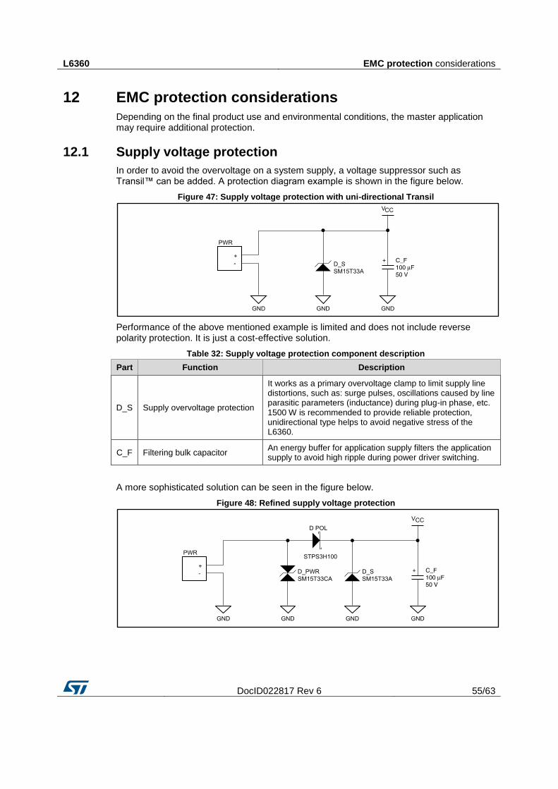
12 EMC protection considerations
Depending on the final product use and environmental conditions, the master application may require additional protection.
12.1 Supply voltage protection
In order to avoid the overvoltage on a system supply, a voltage suppressor such as Transil™ can be added. A protection diagram example is shown in the figure below.
Figure 47: Supply voltage protection with uni-directional Transil
Performance of the above mentioned example is limited and does not include reverse polarity protection. It is just a cost-effective solution.
Table 32: Supply voltage protection component description
Part Function Description
D_S Supply overvoltage protection
It works as a primary overvoltage clamp to limit supply line distortions, such as: surge pulses, oscillations caused by line parasitic parameters (inductance) during plug-in phase, etc. 1500 W is recommended to provide reliable protection, unidirectional type helps to avoid negative stress of the L6360.
C_F Filtering bulk capacitor An energy buffer for application supply filters the application supply to avoid high ripple during power driver switching.
A more sophisticated solution can be seen in the figure below.
Figure 48: Refined supply voltage protection
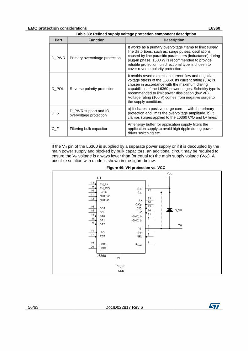
EMC protection considerations L6360
56/63 DocID022817 Rev 6
Table 33: Refined supply voltage protection component description
Part Function Description
D_PWR Primary overvoltage protection
It works as a primary overvoltage clamp to limit supply line distortions, such as: surge pulses, oscillations caused by line parasitic parameters (inductance) during plug-in phase. 1500 W is recommended to provide reliable protection, unidirectional type is chosen to cover reverse polarity protection.
D_POL Reverse polarity protection
It avoids reverse direction current flow and negative voltage stress of the L6360. Its current rating (3 A) is chosen in accordance with the maximum driving capabilities of the L6360 power stages. Schottky type is recommended to limit power dissipation (low VF). Voltage rating (100 V) comes from negative surge to the supply condition.
D_S D_PWR support and IO overvoltage protection
a) It shares a positive surge current with the primary protection and limits the overvoltage amplitude. b) It clamps surges applied to the L6360 C/Q and L+ lines.
C_F Filtering bulk capacitor An energy buffer for application supply filters the application supply to avoid high ripple during power driver switching etc.
If the VH pin of the L6360 is supplied by a separate power supply or if it is decoupled by the main power supply and blocked by bulk capacitors, an additional circuit may be required to ensure the VH voltage is always lower than (or equal to) the main supply voltage (VCC). A possible solution with diode is shown in the figure below.
Figure 49: VH protection vs. VCC
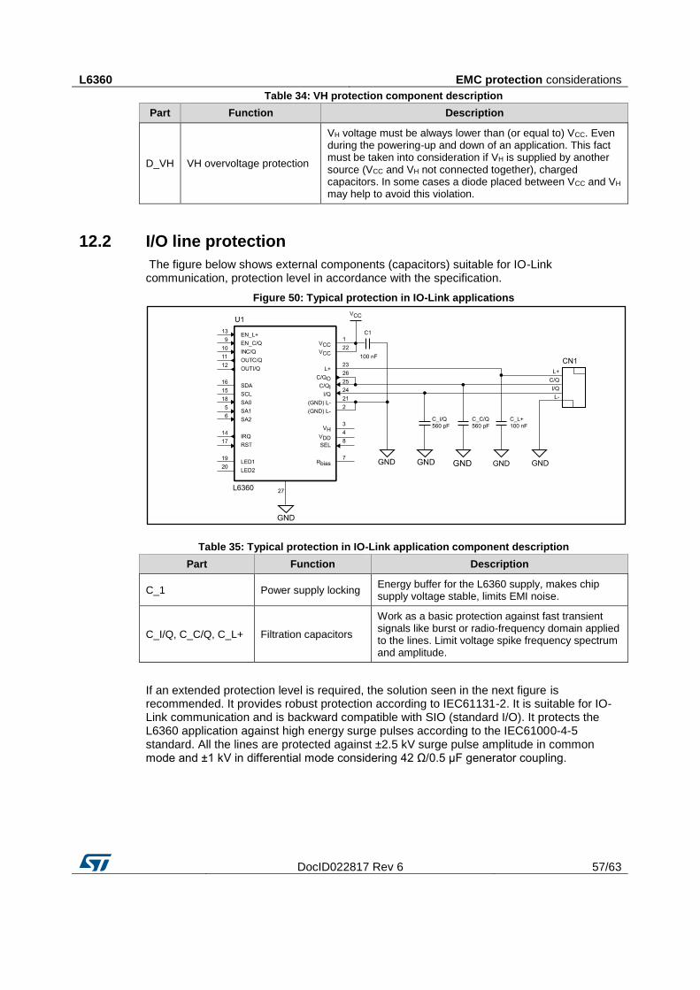
L6360 EMC protection considerations
DocID022817 Rev 6 57/63
Table 34: VH protection component description
Part Function Description
D_VH VH overvoltage protection
VH voltage must be always lower than (or equal to) VCC. Even during the powering-up and down of an application. This fact must be taken into consideration if VH is supplied by another source (VCC and VH not connected together), charged capacitors. In some cases a diode placed between VCC and VH may help to avoid this violation.
12.2 I/O line protection
The figure below shows external components (capacitors) suitable for IO-Link communication, protection level in accordance with the specification.
Figure 50: Typical protection in IO-Link applications
Table 35: Typical protection in IO-Link application component description
Part Function Description
C_1 Power supply locking Energy buffer for the L6360 supply, makes chip supply voltage stable, limits EMI noise.
C_I/Q, C_C/Q, C_L+ Filtration capacitors
Work as a basic protection against fast transient signals like burst or radio-frequency domain applied to the lines. Limit voltage spike frequency spectrum and amplitude.
If an extended protection level is required, the solution seen in the next figure is recommended. It provides robust protection according to IEC61131-2. It is suitable for IO-Link communication and is backward compatible with SIO (standard I/O). It protects the L6360 application against high energy surge pulses according to the IEC61000-4-5 standard. All the lines are protected against ±2.5 kV surge pulse amplitude in common mode and ±1 kV in differential mode considering 42 Ω/0.5 μF generator coupling.
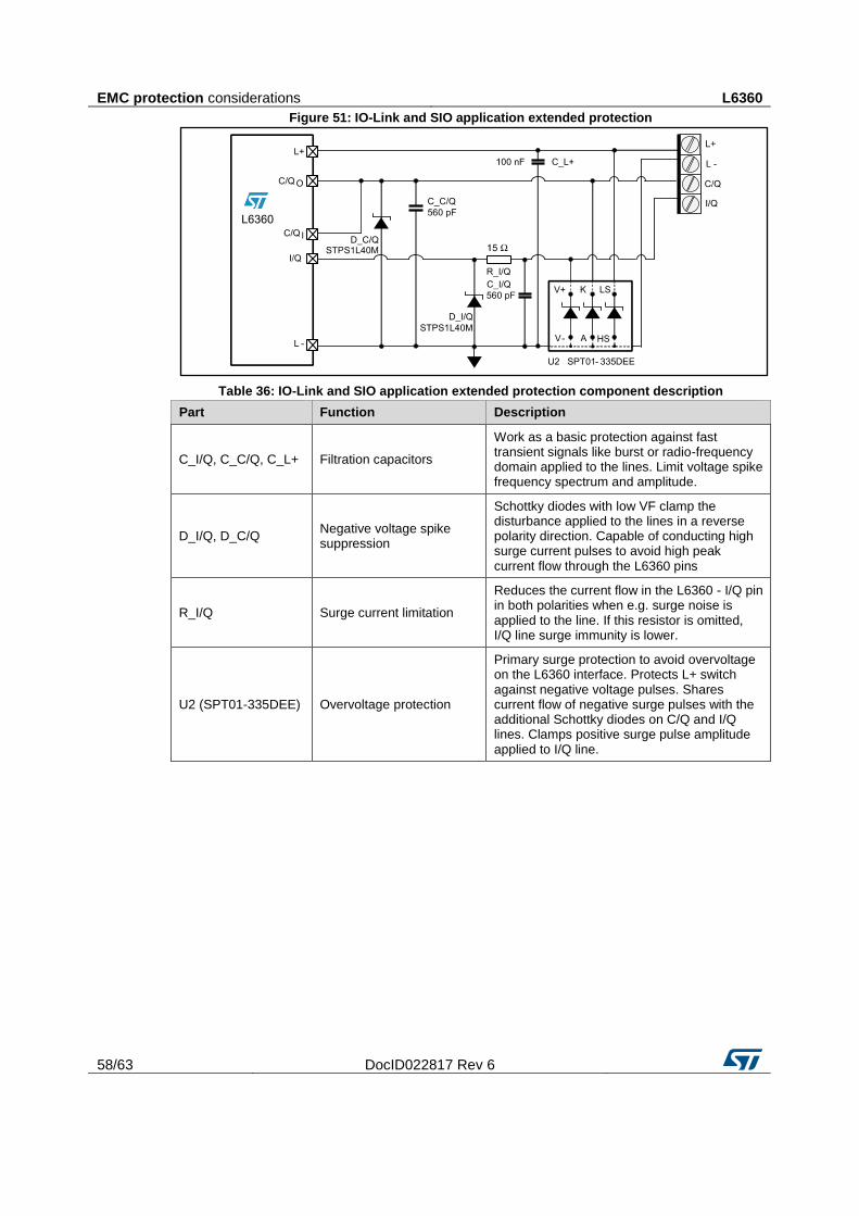
EMC protection considerations L6360
58/63 DocID022817 Rev 6
Figure 51: IO-Link and SIO application extended protection
Table 36: IO-Link and SIO application extended protection component description
Part Function Description
C_I/Q, C_C/Q, C_L+ Filtration capacitors
Work as a basic protection against fast transient signals like burst or radio-frequency domain applied to the lines. Limit voltage spike frequency spectrum and amplitude.
D_I/Q, D_C/Q Negative voltage spike suppression
Schottky diodes with low VF clamp the disturbance applied to the lines in a reverse polarity direction. Capable of conducting high surge current pulses to avoid high peak current flow through the L6360 pins
R_I/Q Surge current limitation
Reduces the current flow in the L6360 - I/Q pin in both polarities when e.g. surge noise is applied to the line. If this resistor is omitted, I/Q line surge immunity is lower.
U2 (SPT01-335DEE) Overvoltage protection
Primary surge protection to avoid overvoltage on the L6360 interface. Protects L+ switch against negative voltage pulses. Shares current flow of negative surge pulses with the additional Schottky diodes on C/Q and I/Q lines. Clamps positive surge pulse amplitude applied to I/Q line.
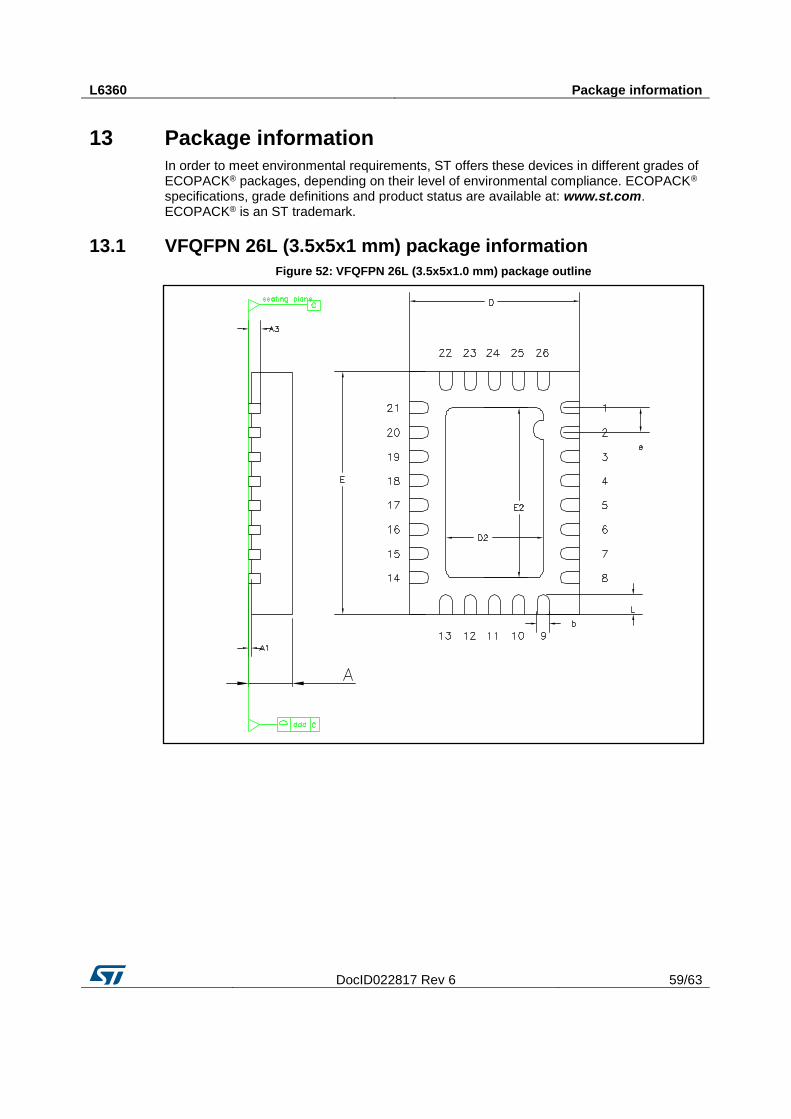
L6360 Package information
DocID022817 Rev 6 59/63
13 Package information
In order to meet environmental requirements, ST offers these devices in different grades of ECOPACK® packages, depending on their level of environmental compliance. ECOPACK® specifications, grade definitions and product status are available at: www.st.com. ECOPACK® is an ST trademark.
13.1 VFQFPN 26L (3.5x5x1 mm) package information
Figure 52: VFQFPN 26L (3.5x5x1.0 mm) package outline
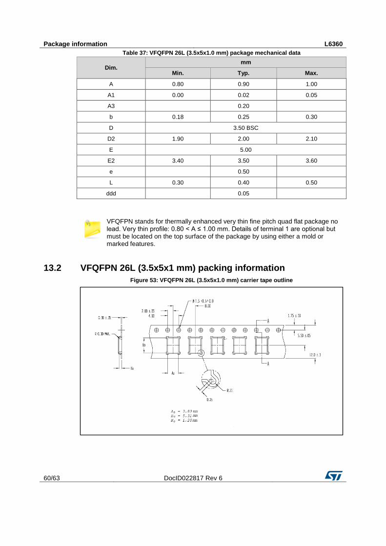
Package information L6360
60/63 DocID022817 Rev 6
Table 37: VFQFPN 26L (3.5x5x1.0 mm) package mechanical data
Dim. mm
Min. Typ. Max.
A 0.80 0.90 1.00
A1 0.00 0.02 0.05
A3
0.20
b 0.18 0.25 0.30
D 3.50 BSC
D2 1.90 2.00 2.10
E 5.00
E2 3.40 3.50 3.60
e
0.50
L 0.30 0.40 0.50
ddd
0.05
VFQFPN stands for thermally enhanced very thin fine pitch quad flat package no lead. Very thin profile: 0.80 < A ≤ 1.00 mm. Details of terminal 1 are optional but must be located on the top surface of the package by using either a mold or marked features.
13.2 VFQFPN 26L (3.5x5x1 mm) packing information
Figure 53: VFQFPN 26L (3.5x5x1.0 mm) carrier tape outline
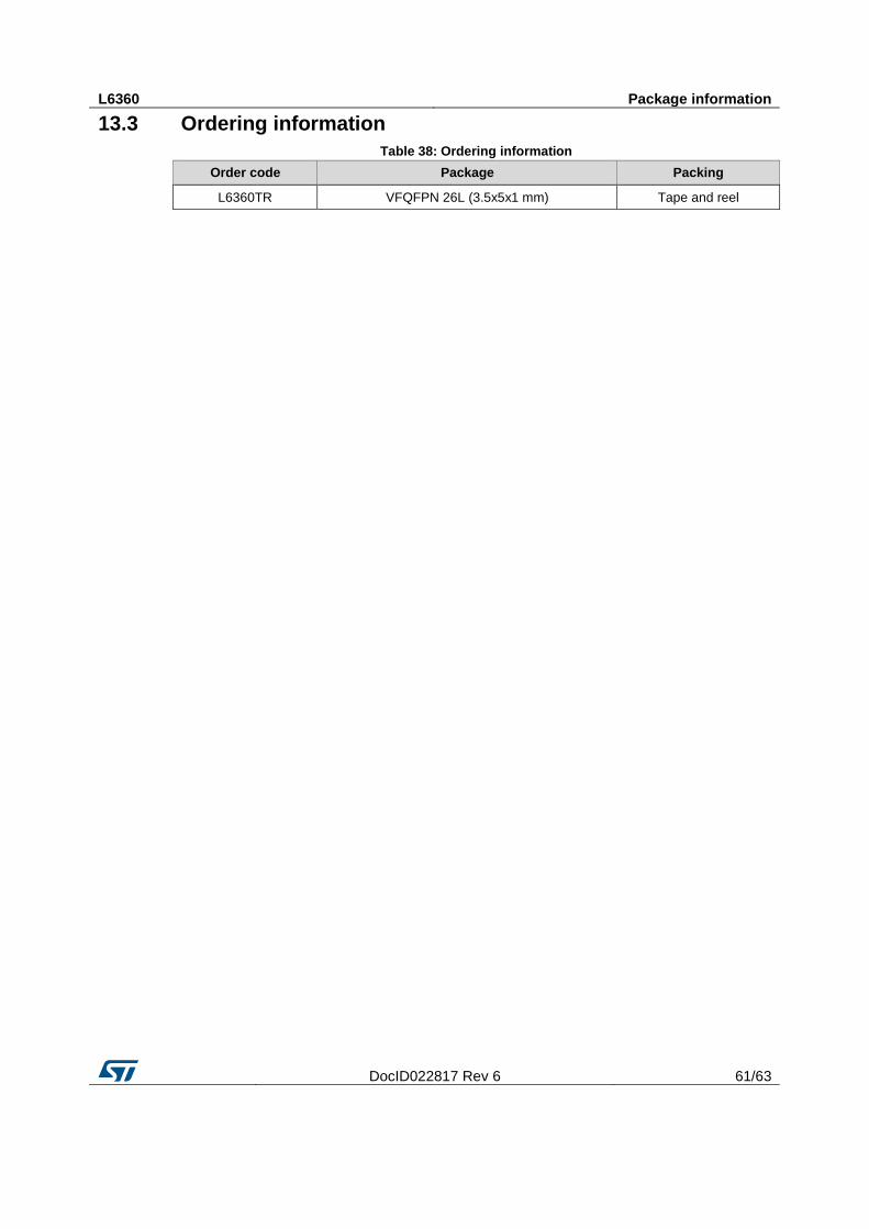
L6360 Package information
DocID022817 Rev 6 61/63
13.3 Ordering information
Table 38: Ordering information
Order code Package Packing
L6360TR VFQFPN 26L (3.5x5x1 mm) Tape and reel
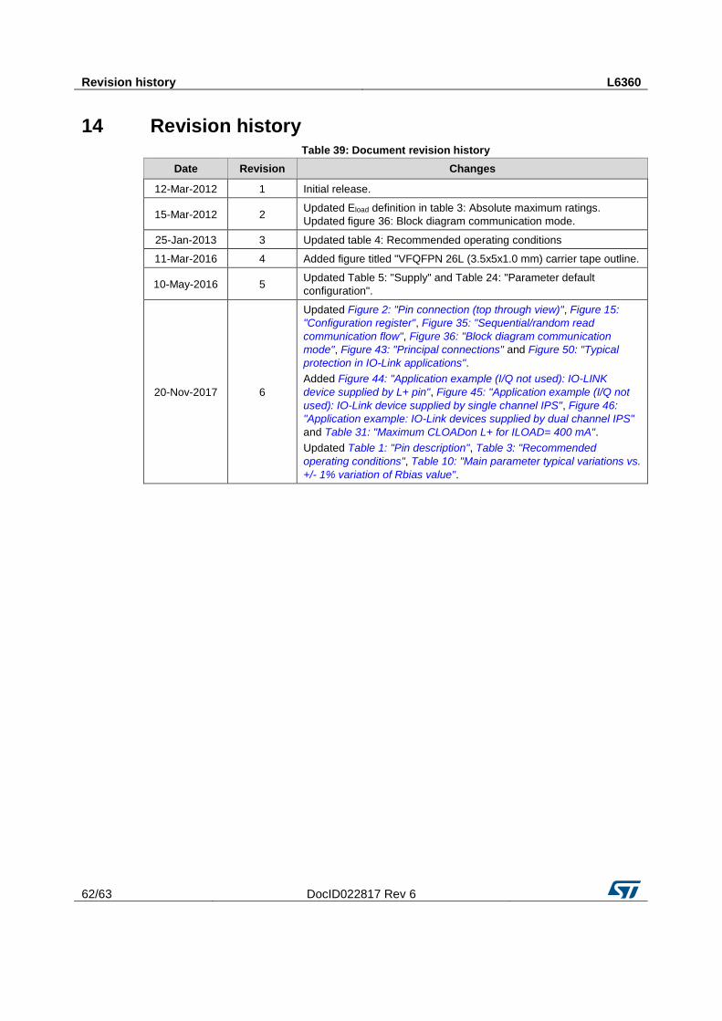
Revision history L6360
62/63 DocID022817 Rev 6
14 Revision history Table 39: Document revision history
Date Revision Changes
12-Mar-2012 1 Initial release.
15-Mar-2012 2 Updated Eload definition in table 3: Absolute maximum ratings.
Updated figure 36: Block diagram communication mode.
25-Jan-2013 3 Updated table 4: Recommended operating conditions
11-Mar-2016 4 Added figure titled "VFQFPN 26L (3.5x5x1.0 mm) carrier tape outline.
10-May-2016 5 Updated Table 5: "Supply" and Table 24: "Parameter default
configuration".
20-Nov-2017 6
Updated Figure 2: "Pin connection (top through view)", Figure 15:
"Configuration register", Figure 35: "Sequential/random read
communication flow", Figure 36: "Block diagram communication
mode", Figure 43: "Principal connections" and Figure 50: "Typical
protection in IO-Link applications".
Added Figure 44: "Application example (I/Q not used): IO-LINK
device supplied by L+ pin", Figure 45: "Application example (I/Q not
used): IO-Link device supplied by single channel IPS", Figure 46:
"Application example: IO-Link devices supplied by dual channel IPS"
and Table 31: "Maximum CLOADon L+ for ILOAD= 400 mA".
Updated Table 1: "Pin description", Table 3: "Recommended
operating conditions", Table 10: "Main parameter typical variations vs.
+/- 1% variation of Rbias value".
L6360
DocID022817 Rev 6 63/63
IMPORTANT NOTICE – PLEASE READ CAREFULLY
STMicroelectronics NV and its subsidiaries (“ST”) reserve the right to make changes, corrections, enhancements, modifications, and improvements to ST products and/or to this document at any time without notice. Purchasers should obtain the latest relevant information on ST products before placing orders. ST products are sold pursuant to ST’s terms and conditions of sale in place at the time of order acknowledgement.
Purchasers are solely responsible for the choice, selection, and use of ST products and ST assumes no liability for application assistance or the design of Purchasers’ products.
No license, express or implied, to any intellectual property right is granted by ST herein.
Resale of ST products with provisions different from the information set forth herein shall void any warranty granted by ST for such product.
ST and the ST logo are trademarks of ST. All other product or service names are the property of their respective owners.
Information in this document supersedes and replaces information previously supplied in any prior versions of this document.
© 2017 STMicroelectronics – All rights reserved


![CALORIMETRIE. Warmtehoeveelheid Q Eenheid: [Q] = J (joule) koudwarm T1T1 T2T2 TeTe QoQo QaQa Warmtebalans: Q opgenomen = Q afgestaan Evenwichtstemperatuur:](https://static.fdocument.org/doc/165x107/5551a0f04979591f3c8bac13/calorimetrie-warmtehoeveelheid-q-eenheid-q-j-joule-koudwarm-t1t1-t2t2-tete-qoqo-qaqa-warmtebalans-q-opgenomen-q-afgestaan-evenwichtstemperatuur.jpg)


![50 IChO 2018 - pianetachimica.it · oΔG = ΔG + RT lnQ Quoziente di reazione Q Per la reazione a A + b B ⇌ c C + d D: Q = [C]c[D]d [A]a[B]b Variazione di entropia: rev ΔS = q](https://static.fdocument.org/doc/165x107/5c6a38b109d3f2310b8c475f/50-icho-2018-og-g-rt-lnq-quoziente-di-reazione-q-per-la-reazione-a.jpg)


![EXN3000 xsΘXR w M wⁿ - IBM€¦ · Q Γ ΓLYM5 MH6 H10 Γ AN yw [e C lNo Ω≥C 3. b≈[I AN ywb BJ 2 PEIA mW]TwwAϕaíJw PC Q Γ ΓL YM5 MH5 H11 Γ AN yw [WC lNo Ω≥C 4. bww](https://static.fdocument.org/doc/165x107/5f67ed909697ab24a764073f/exn3000-xsxr-w-m-wa-ibm-q-lym5-mh6-h10-an-yw-e-c-lno-ac-3-bai.jpg)