Ο βοτανικός κήπος του 11ου Νηπιαγωγείου Χανίων/ 11th nipiagogio chanion herb garden
Introducing PowerAmerica at the 11th Annual SiC MOS workshopDr. Victor Veliadis, CTO
Mission Summary
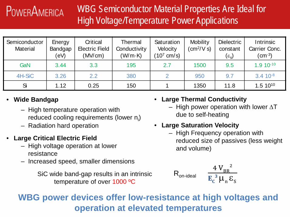
Semiconductor Material
Energy Bandgap
(eV)
Critical Electric Field
(MV/cm)
Thermal Conductivity
(W/m·K)
Saturation Velocity
(107 cm/s)
Mobility (cm2/V s)
Dielectric constant
(εs)
Intrinsic Carrier Conc.
(cm-3)
GaN 3.44 3.3 195 2.7 1500 9.5 1.9 10-10
4H-SiC 3.26 2.2 380 2 950 9.7 3.4 10-8
Si 1.12 0.25 150 1 1350 11.8 1.5 1010
WBG power devices offer low-resistance at high voltages and operation at elevated temperatures
• Wide Bandgap– High temperature operation with
reduced cooling requirements (lower ni)– Radiation hard operation
• Large Critical Electric Field– High voltage operation at lower
resistance – Increased speed, smaller dimensions
• Large Thermal Conductivity– High power operation with lower ∆T
due to self-heating• Large Saturation Velocity
– High Frequency operation with reduced size of passives (less weight and volume)
Ron-ideal =4 VBR
2
𝐄𝐄𝐂𝐂𝟑𝟑µn εS
SiC wide band-gap results in an intrinsic temperature of over 1000 ºC
WBG Semiconductor Material Properties Are Ideal for High Voltage/Temperature Power Applications
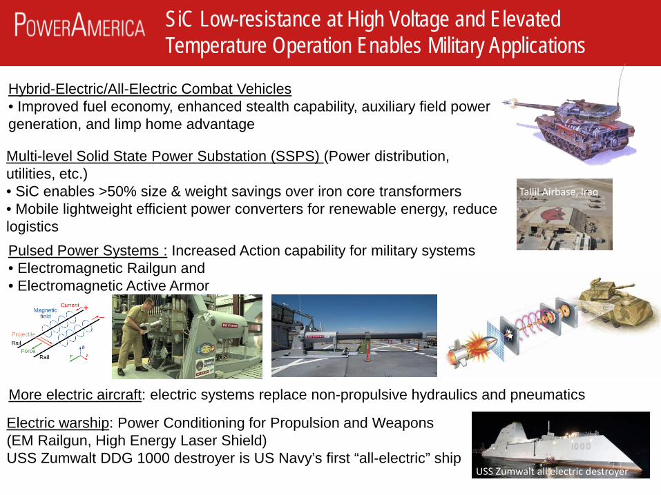
SiC Low-resistance at High Voltage and Elevated Temperature Operation Enables Military Applications
Multi-level Solid State Power Substation (SSPS) (Power distribution, utilities, etc.)• SiC enables >50% size & weight savings over iron core transformers• Mobile lightweight efficient power converters for renewable energy, reduce logistics
Hybrid-Electric/All-Electric Combat Vehicles• Improved fuel economy, enhanced stealth capability, auxiliary field power generation, and limp home advantage
Tallil Airbase, Iraq
More electric aircraft: electric systems replace non-propulsive hydraulics and pneumatics
Electric warship: Power Conditioning for Propulsion and Weapons (EM Railgun, High Energy Laser Shield)USS Zumwalt DDG 1000 destroyer is US Navy’s first “all-electric” ship
USS Zumwalt all electric destroyer
Pulsed Power Systems : Increased Action capability for military systems• Electromagnetic Railgun and • Electromagnetic Active Armor
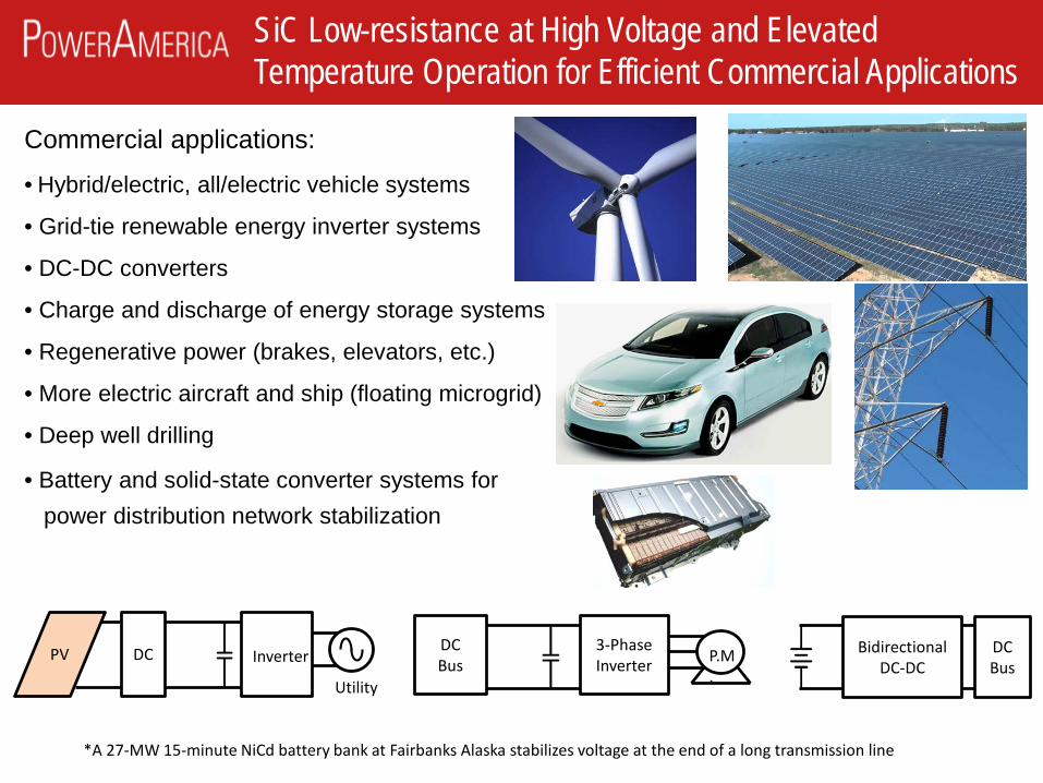
SiC Low-resistance at High Voltage and Elevated Temperature Operation for Efficient Commercial Applications
Commercial applications:
• Hybrid/electric, all/electric vehicle systems
• Grid-tie renewable energy inverter systems
• DC-DC converters
• Charge and discharge of energy storage systems
• Regenerative power (brakes, elevators, etc.)
• More electric aircraft and ship (floating microgrid)
• Deep well drilling
• Battery and solid-state converter systems for power distribution network stabilization
P.M.
3-PhaseInverter
DCBus
DCBus
BidirectionalDC-DC
DCPV
Utility
Inverter
*A 27-MW 15-minute NiCd battery bank at Fairbanks Alaska stabilizes voltage at the end of a long transmission line
Mission SummaryPowerAmerica is a U.S Department of Energy WBG Semiconductor Manufacturing Institute
• The U.S Department of Energy launched the PowerAmerica Institute under the initiative of National Network of Manufacturing Institutes (NNMI) to commercialize Wide Band Gap (WBG) power devices.
• PowerAmerica is being managed by North Carolina State University.
• PowerAmerica is accelerating commercialization of wide bandgap semiconductor technologies by making them cost-competitive with silicon-based power electronics and reducing their perceived risk in industrial applications.
• Through participation in the PowerAmerica ecosystem, industry members grow their business by accelerated wide bandgap product introduction to market and University members gain by engaging in collaborative projects with industry.
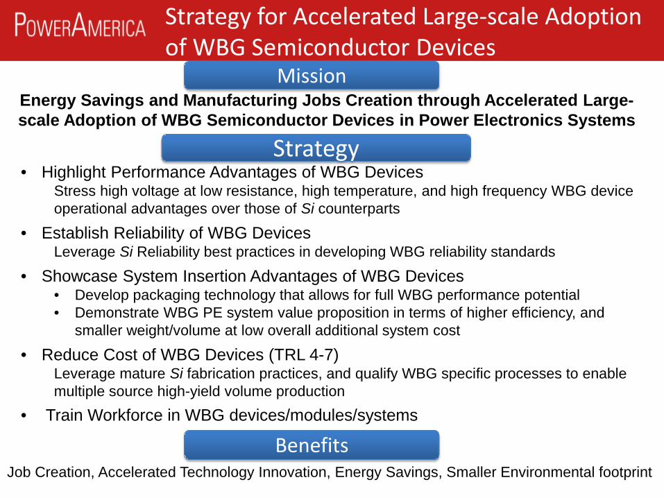
Mission SummaryStrategy for Accelerated Large-scale Adoption of WBG Semiconductor Devices
Benefits
Strategy
Mission
• Highlight Performance Advantages of WBG DevicesStress high voltage at low resistance, high temperature, and high frequency WBG device operational advantages over those of Si counterparts
• Establish Reliability of WBG DevicesLeverage Si Reliability best practices in developing WBG reliability standards
• Showcase System Insertion Advantages of WBG Devices• Develop packaging technology that allows for full WBG performance potential• Demonstrate WBG PE system value proposition in terms of higher efficiency, and
smaller weight/volume at low overall additional system cost
• Reduce Cost of WBG Devices (TRL 4-7)Leverage mature Si fabrication practices, and qualify WBG specific processes to enable multiple source high-yield volume production
• Train Workforce in WBG devices/modules/systems
Energy Savings and Manufacturing Jobs Creation through Accelerated Large-scale Adoption of WBG Semiconductor Devices in Power Electronics Systems
Job Creation, Accelerated Technology Innovation, Energy Savings, Smaller Environmental footprint
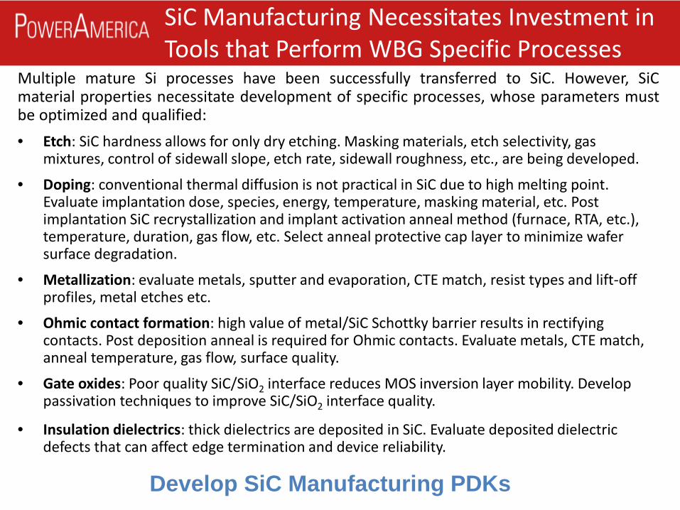
Mission SummarySiC Manufacturing Necessitates Investment in Tools that Perform WBG Specific Processes
Multiple mature Si processes have been successfully transferred to SiC. However, SiCmaterial properties necessitate development of specific processes, whose parameters mustbe optimized and qualified:• Etch: SiC hardness allows for only dry etching. Masking materials, etch selectivity, gas
mixtures, control of sidewall slope, etch rate, sidewall roughness, etc., are being developed.
• Doping: conventional thermal diffusion is not practical in SiC due to high melting point. Evaluate implantation dose, species, energy, temperature, masking material, etc. Post implantation SiC recrystallization and implant activation anneal method (furnace, RTA, etc.), temperature, duration, gas flow, etc. Select anneal protective cap layer to minimize wafer surface degradation.
• Metallization: evaluate metals, sputter and evaporation, CTE match, resist types and lift-off profiles, metal etches etc.
• Ohmic contact formation: high value of metal/SiC Schottky barrier results in rectifying contacts. Post deposition anneal is required for Ohmic contacts. Evaluate metals, CTE match, anneal temperature, gas flow, surface quality.
• Gate oxides: Poor quality SiC/SiO2 interface reduces MOS inversion layer mobility. Develop passivation techniques to improve SiC/SiO2 interface quality.
• Insulation dielectrics: thick dielectrics are deposited in SiC. Evaluate deposited dielectric defects that can affect edge termination and device reliability.
Develop SiC Manufacturing PDKs

Mission SummaryX-FAB Leverages Si Infrastructure and SiC Tool Investment to Offer SiC Manufacturing Services
• Leverage Existing investment In Capital Equipment.
• Leverage an existing highly trained workforce
• Benefit from existing experience in offering qualified products
• Increase yield from implementation of quality control.
SiC JBS diodes, BJTs, and MOSFETs presently fabricated at XFAB
X-FAB SiC Users: ABB, GeneSiC, Monolith, NCSU, USCi
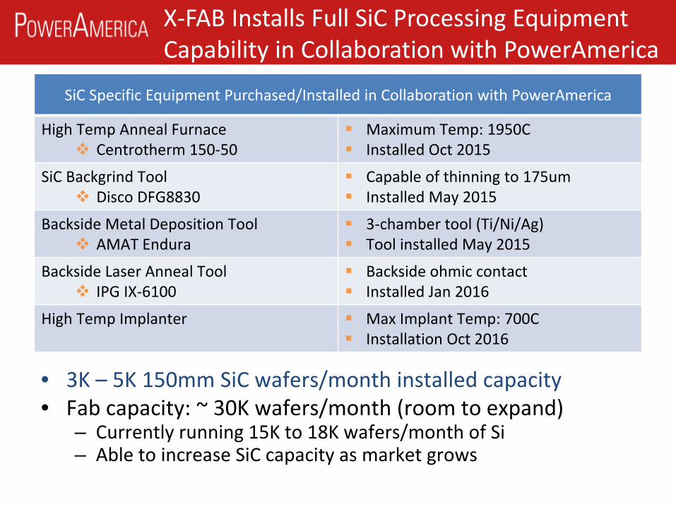
SiC Specific Equipment Purchased/Installed in Collaboration with PowerAmerica
High Temp Anneal Furnace Centrotherm 150-50
Maximum Temp: 1950C Installed Oct 2015
SiC Backgrind Tool Disco DFG8830
Capable of thinning to 175um Installed May 2015
Backside Metal Deposition Tool AMAT Endura
3-chamber tool (Ti/Ni/Ag) Tool installed May 2015
Backside Laser Anneal Tool IPG IX-6100
Backside ohmic contact Installed Jan 2016
High Temp Implanter Max Implant Temp: 700C Installation Oct 2016
• 3K – 5K 150mm SiC wafers/month installed capacity• Fab capacity: ~ 30K wafers/month (room to expand)
– Currently running 15K to 18K wafers/month of Si– Able to increase SiC capacity as market grows
Mission SummaryX-FAB Installs Full SiC Processing Equipment Capability in Collaboration with PowerAmerica
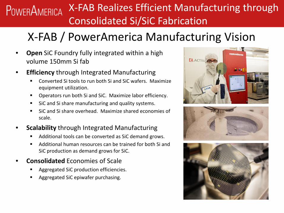
• Open SiC Foundry fully integrated within a high volume 150mm Si fab
• Efficiency through Integrated Manufacturing Converted Si tools to run both Si and SiC wafers. Maximize
equipment utilization. Operators run both Si and SiC. Maximize labor efficiency. SiC and Si share manufacturing and quality systems. SiC and Si share overhead. Maximize shared economies of
scale.
• Scalability through Integrated Manufacturing Additional tools can be converted as SiC demand grows. Additional human resources can be trained for both Si and
SiC production as demand grows for SiC.
• Consolidated Economies of Scale Aggregated SiC production efficiencies. Aggregated SiC epiwafer purchasing.
X-FAB / PowerAmerica Manufacturing Vision
Mission SummaryX-FAB Realizes Efficient Manufacturing through Consolidated Si/SiC Fabrication
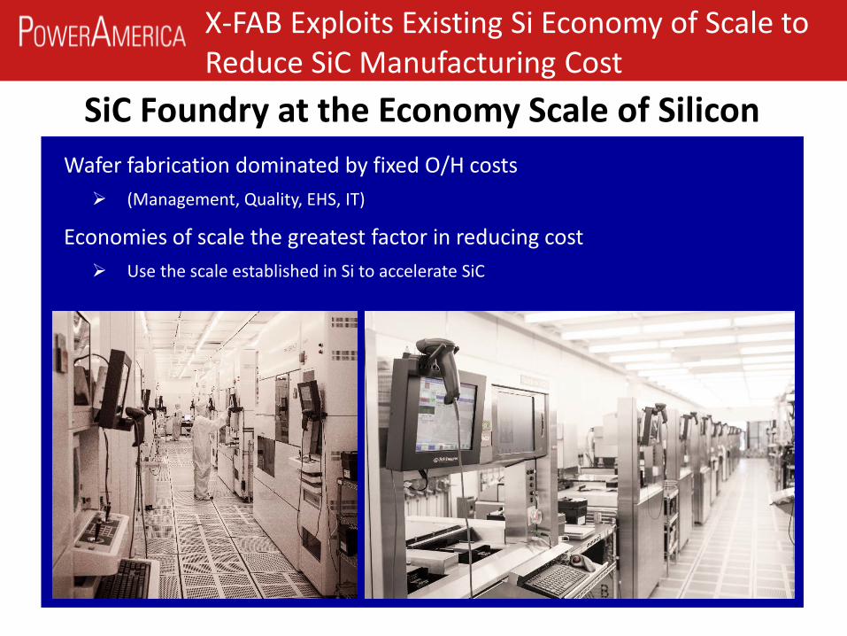
SiC Foundry at the Economy Scale of SiliconWafer fabrication dominated by fixed O/H costs (Management, Quality, EHS, IT)
Economies of scale the greatest factor in reducing cost Use the scale established in Si to accelerate SiC
Mission SummaryX-FAB Exploits Existing Si Economy of Scale to Reduce SiC Manufacturing Cost
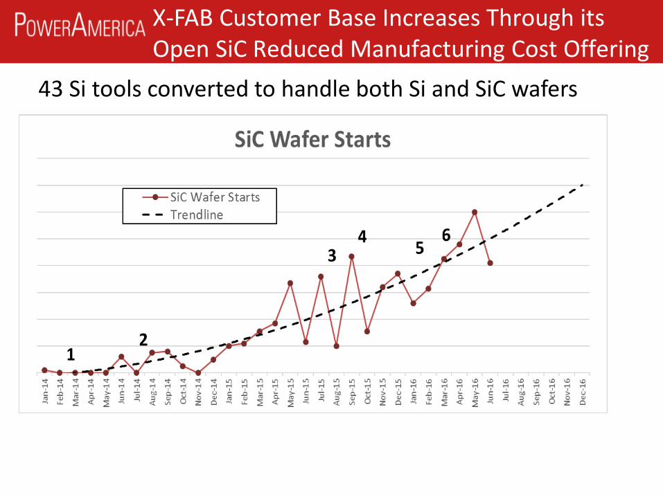
43 Si tools converted to handle both Si and SiC wafers
Mission SummaryX-FAB Customer Base Increases Through its Open SiC Reduced Manufacturing Cost Offering
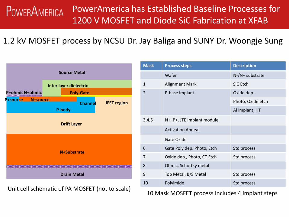
Mission SummaryPowerAmerica has Established Baseline Processes for 1200 V MOSFET and Diode SiC Fabrication at XFAB
P+ohmicInter layer dielectric
Poly-Gate
P-body
N+sourceP+sourceChannel JFET region
N+ohmic
Drift Layer
N+Substrate
Source Metal
Drain Metal
Mask Process steps Description
Wafer N-/N+ substrate
1 Alignment Mark SiC Etch
2 P-base implant Oxide dep.
Photo, Oxide etch
Al implant, HT
3,4,5 N+, P+, JTE implant module
Activation Anneal
Gate Oxide
6 Gate Poly dep. Photo, Etch Std process
7 Oxide dep., Photo, CT Etch Std process
8 Ohmic, Schottky metal
9 Top Metal, B/S Metal Std process
10 Polyimide Std process
10 Mask MOSFET process includes 4 implant steps
1.2 kV MOSFET process by NCSU Dr. Jay Baliga and SUNY Dr. Woongje Sung
Unit cell schematic of PA MOSFET (not to scale)
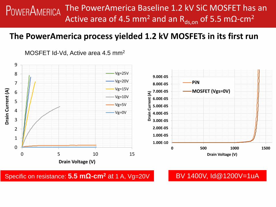
Mission SummaryThe PowerAmerica Baseline 1.2 kV SiC MOSFET has an Active area of 4.5 mm2 and an Rds,on of 5.5 mΩ-cm2
0
1
2
3
4
5
6
7
8
9
0 5 10 15
Drai
n Cu
rren
t (A)
Drain Voltage (V)
Vg=25V
Vg=20V
Vg=15V
Vg=10V
Vg=5V
Vg=0V
Specific on resistance: 5.5 mΩ-cm2 at 1 A, Vg=20V
MOSFET Id-Vd, Active area 4.5 mm2
The PowerAmerica process yielded 1.2 kV MOSFETs in its first run
1.00E-10
1.00E-05
2.00E-05
3.00E-05
4.00E-05
5.00E-05
6.00E-05
7.00E-05
8.00E-05
9.00E-05
0 500 1000 1500Dr
ain
Curr
ent (
A)Drain Voltage (V)
PiN
MOSFET (Vgs=0V)
BV 1400V, Id@1200V=1uA
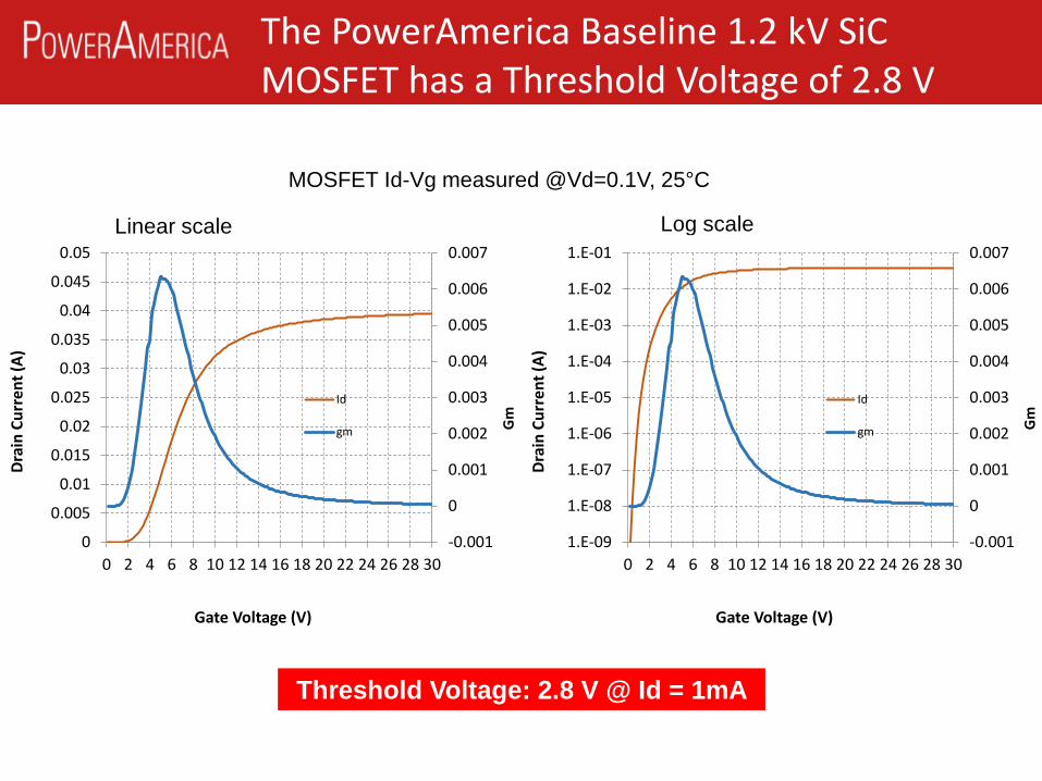
Mission SummaryThe PowerAmerica Baseline 1.2 kV SiCMOSFET has a Threshold Voltage of 2.8 V
MOSFET Id-Vg measured @Vd=0.1V, 25°C
Threshold Voltage: 2.8 V @ Id = 1mA
Linear scale Log scale
-0.001
0
0.001
0.002
0.003
0.004
0.005
0.006
0.007
0
0.005
0.01
0.015
0.02
0.025
0.03
0.035
0.04
0.045
0.05
0 2 4 6 8 10 12 14 16 18 20 22 24 26 28 30
Drai
n Cu
rren
t (A)
Gate Voltage (V)
Id
gm Gm
-0.001
0
0.001
0.002
0.003
0.004
0.005
0.006
0.007
1.E-09
1.E-08
1.E-07
1.E-06
1.E-05
1.E-04
1.E-03
1.E-02
1.E-01
0 2 4 6 8 10 12 14 16 18 20 22 24 26 28 30Dr
ain
Curr
ent (
A)
Gate Voltage (V)
Id
gm Gm
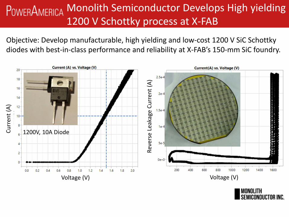
Mission SummaryMonolith Semiconductor Develops High yielding 1200 V Schottky process at X-FAB
Reve
rse
Leak
age
Curr
ent (
A)
Voltage (V)
Curr
ent (
A)
1200V, 10A Diode
Voltage (V)
Objective: Develop manufacturable, high yielding and low-cost 1200 V SiC Schottky diodes with best-in-class performance and reliability at X-FAB’s 150-mm SiC foundry.
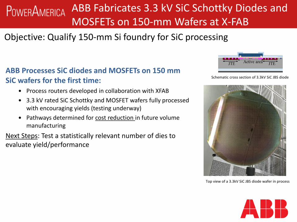
Mission SummaryABB Fabricates 3.3 kV SiC Schottky Diodes and MOSFETs on 150-mm Wafers at X-FAB
Top view of a 3.3kV SiC JBS diode wafer in process
ABB Processes SiC diodes and MOSFETs on 150 mm SiC wafers for the first time:
Process routers developed in collaboration with XFAB 3.3 kV rated SiC Schottky and MOSFET wafers fully processed
with encouraging yields (testing underway) Pathways determined for cost reduction in future volume
manufacturing
Next Steps: Test a statistically relevant number of dies to evaluate yield/performance
Schematic cross section of 3.3kV SiC JBS diode
Objective: Qualify 150-mm Si foundry for SiC processing
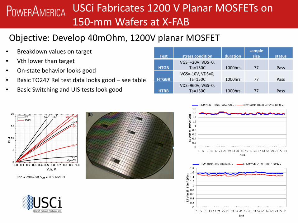
Mission SummaryUSCi Fabricates 1200 V Planar MOSFETs on 150-mm Wafers at X-FAB
Objective: Develop 40mOhm, 1200V planar MOSFET• Breakdown values on target• Vth lower than target• On-state behavior looks good • Basic TO247 Rel test data looks good – see table• Basic Switching and UIS tests look good
Test stress condition duration sample
size status
HTGBVGS=+20V, VDS=0,
Ta=150C 1000hrs 77 Pass
HTGBRVGS=-10V, VDS=0,
Ta=150C 1000hrs 77 Pass
HTRBVDS=960V, VGS=0,
Ta=150C 1000hrs 77 Pass
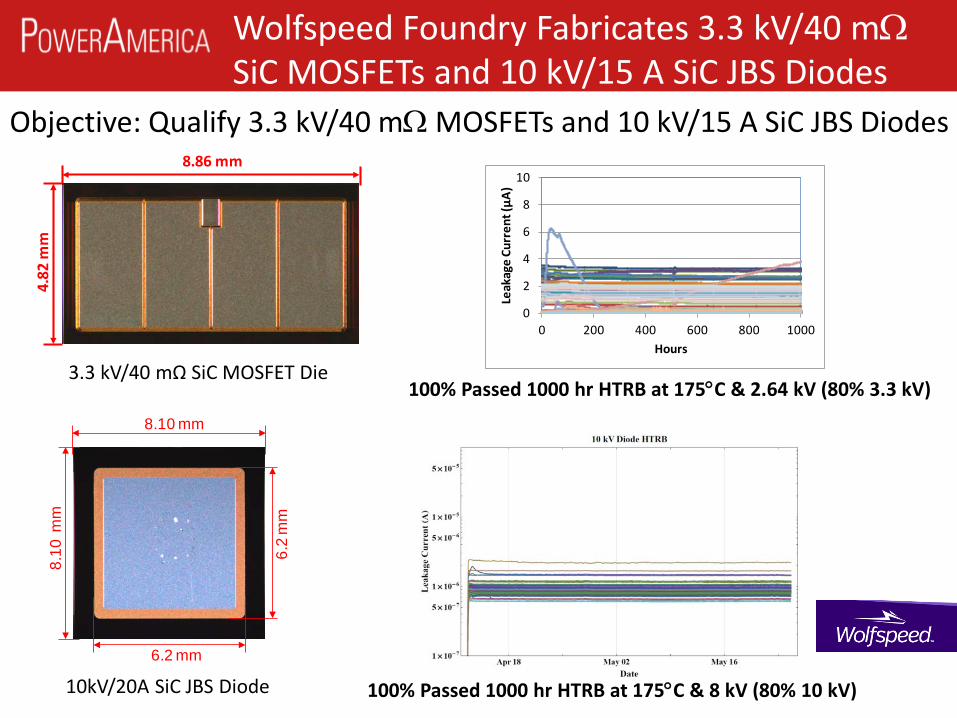
Mission SummaryWolfspeed Foundry Fabricates 3.3 kV/40 mΩSiC MOSFETs and 10 kV/15 A SiC JBS Diodes
Objective: Qualify 3.3 kV/40 mΩ MOSFETs and 10 kV/15 A SiC JBS Diodes
8.10 mm
8.10
mm
6.2 mm
6.2
mm
10kV/20A SiC JBS Diode 100% Passed 1000 hr HTRB at 175°C & 8 kV (80% 10 kV)
0
2
4
6
8
10
0 200 400 600 800 1000
Leak
age
Curr
ent (
µA)
Hours
8.86 mm
4.82
mm
3.3 kV/40 mΩ SiC MOSFET Die 100% Passed 1000 hr HTRB at 175°C & 2.64 kV (80% 3.3 kV)
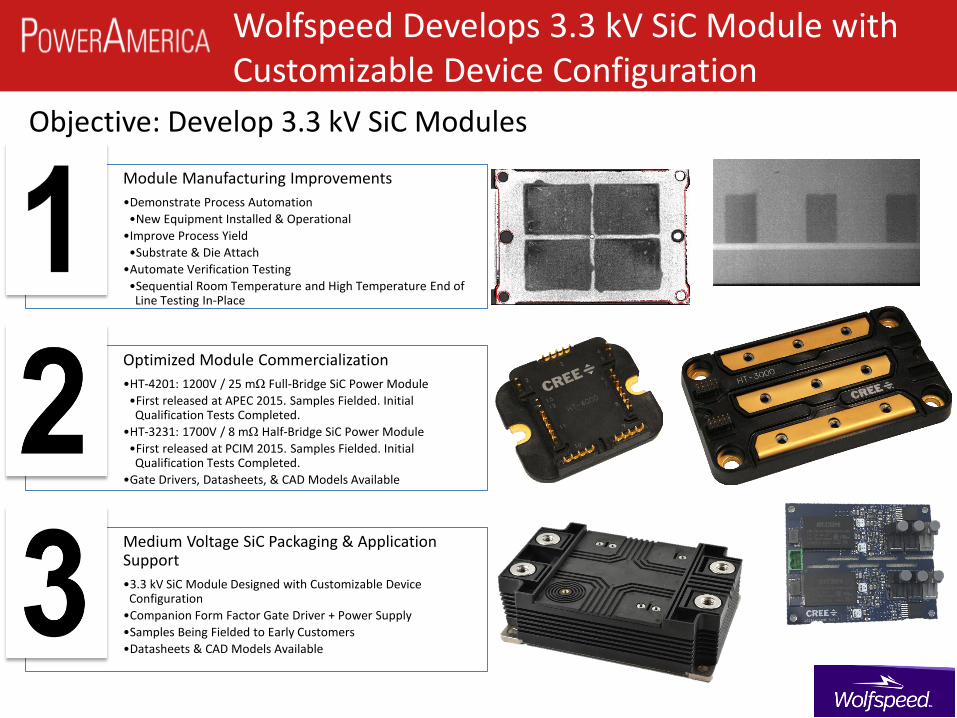
Mission SummaryWolfspeed Develops 3.3 kV SiC Module with Customizable Device Configuration
Module Manufacturing Improvements•Demonstrate Process Automation
•New Equipment Installed & Operational•Improve Process Yield
•Substrate & Die Attach•Automate Verification Testing
•Sequential Room Temperature and High Temperature End of Line Testing In-Place
Optimized Module Commercialization•HT-4201: 1200V / 25 mΩ Full-Bridge SiC Power Module
•First released at APEC 2015. Samples Fielded. Initial Qualification Tests Completed.
•HT-3231: 1700V / 8 mΩ Half-Bridge SiC Power Module•First released at PCIM 2015. Samples Fielded. Initial Qualification Tests Completed.
•Gate Drivers, Datasheets, & CAD Models Available
Medium Voltage SiC Packaging & Application Support•3.3 kV SiC Module Designed with Customizable Device
Configuration•Companion Form Factor Gate Driver + Power Supply•Samples Being Fielded to Early Customers•Datasheets & CAD Models Available
Objective: Develop 3.3 kV SiC Modules
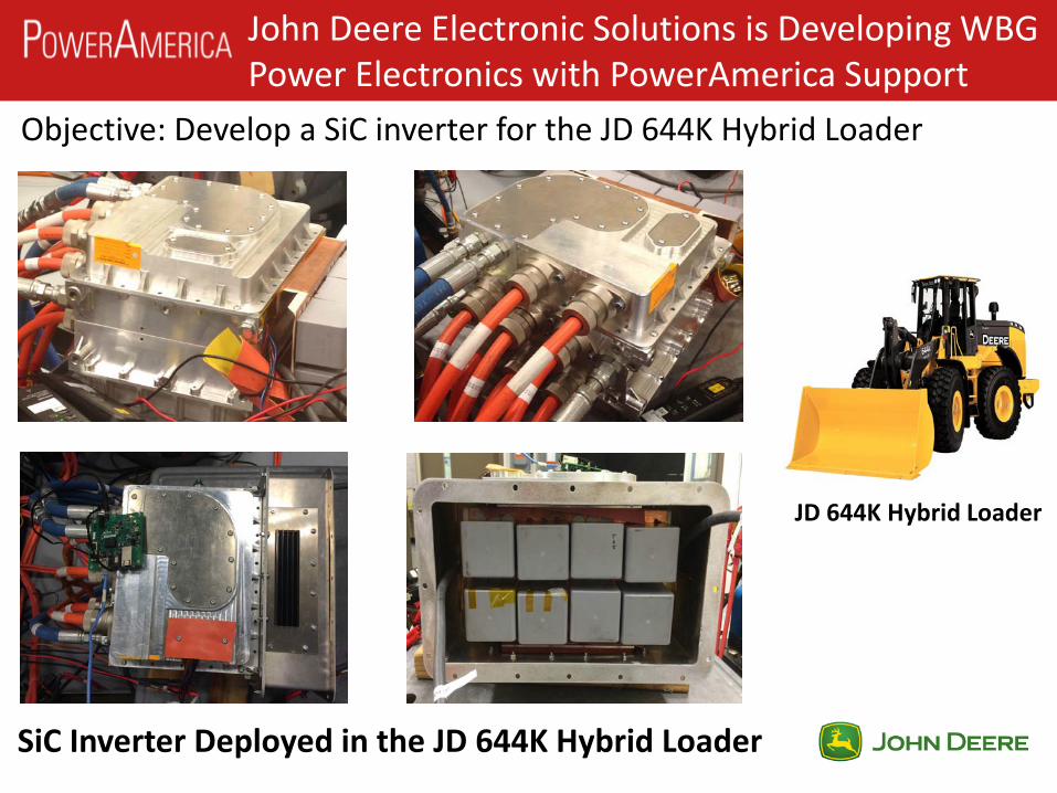
Mission SummaryJohn Deere Electronic Solutions is Developing WBG Power Electronics with PowerAmerica Support
SiC Inverter Deployed in the JD 644K Hybrid Loader
Objective: Develop a SiC inverter for the JD 644K Hybrid Loader
JD 644K Hybrid Loader
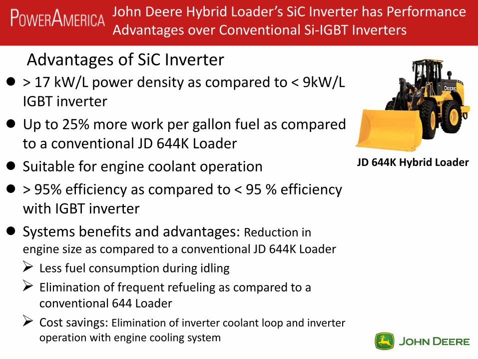
Mission SummaryJohn Deere Hybrid Loader’s SiC Inverter has Performance Advantages over Conventional Si-IGBT Inverters
JD 644K Hybrid Loader
> 17 kW/L power density as compared to < 9kW/L IGBT inverter
Up to 25% more work per gallon fuel as compared to a conventional JD 644K Loader
Suitable for engine coolant operation > 95% efficiency as compared to < 95 % efficiency
with IGBT inverter Systems benefits and advantages: Reduction in
engine size as compared to a conventional JD 644K Loader Less fuel consumption during idling Elimination of frequent refueling as compared to a
conventional 644 Loader Cost savings: Elimination of inverter coolant loop and inverter
operation with engine cooling system
Advantages of SiC Inverter
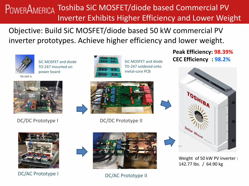
Mission SummaryToshiba SiC MOSFET/diode based Commercial PV Inverter Exhibits Higher Efficiency and Lower Weight
DC/DC Prototype I DC/DC Prototype II
DC/AC Prototype I DC/AC Prototype II
Peak Efficiency: 98.39%CEC Efficiency : 98.2%
Weight of 50 kW PV inverter : 142.77 lbs. / 64.90 kg
SiC MOSFET and diodeTO-247 mounted on power board
SiC MOSFET and diodeTO-247 soldered onto metal-core PCB
Objective: Build SiC MOSFET/diode based 50 kW commercial PV inverter prototypes. Achieve higher efficiency and lower weight.
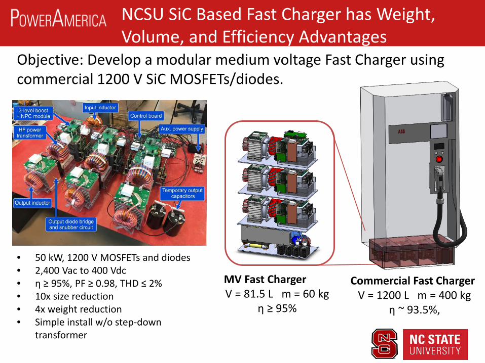
Mission SummaryNCSU SiC Based Fast Charger has Weight, Volume, and Efficiency Advantages
Objective: Develop a modular medium voltage Fast Charger using commercial 1200 V SiC MOSFETs/diodes.
• 50 kW, 1200 V MOSFETs and diodes• 2,400 Vac to 400 Vdc• η ≥ 95%, PF ≥ 0.98, THD ≤ 2%• 10x size reduction • 4x weight reduction• Simple install w/o step-down
transformer
MV Fast ChargerV = 81.5 L m = 60 kg
η ≥ 95%
Commercial Fast ChargerV = 1200 L m = 400 kg
η ~ 93.5%,
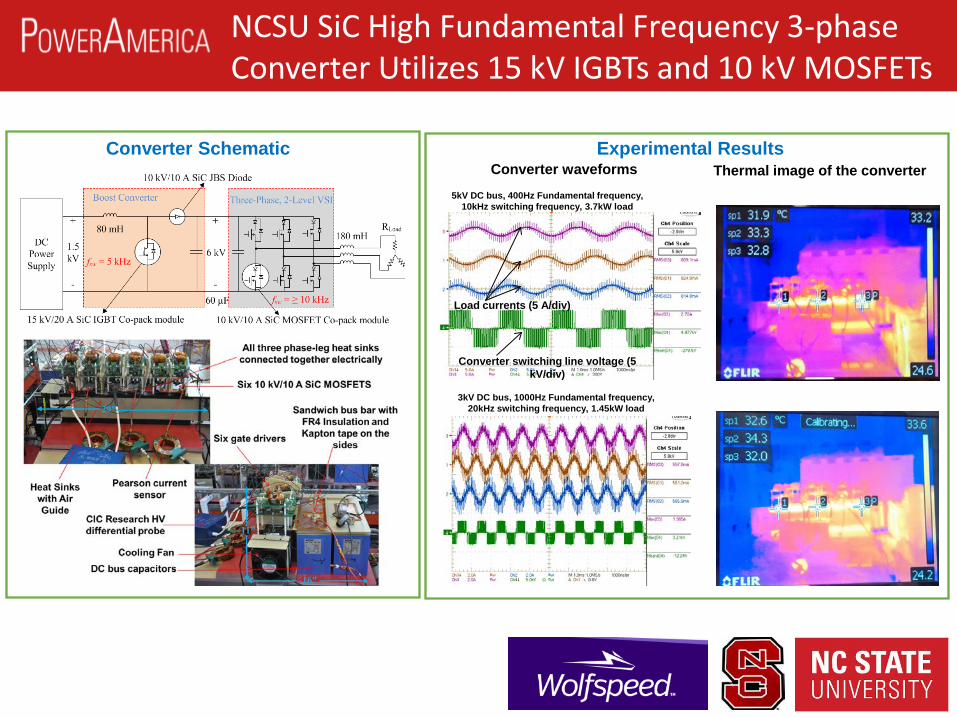
Mission SummaryNCSU SiC High Fundamental Frequency 3-phase Converter Utilizes 15 kV IGBTs and 10 kV MOSFETs
Experimental ResultsConverter Schematic
Load currents (5 A/div)
Converter switching line voltage (5 kV/div)
Converter waveforms Thermal image of the converter5kV DC bus, 400Hz Fundamental frequency,
10kHz switching frequency, 3.7kW load
3kV DC bus, 1000Hz Fundamental frequency, 20kHz switching frequency, 1.45kW load
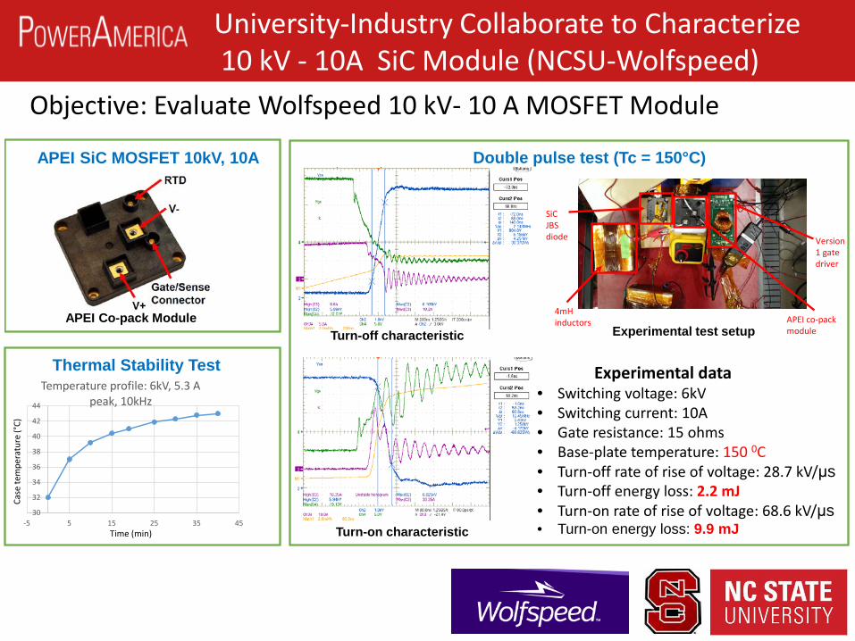
Mission SummaryUniversity-Industry Collaborate to Characterize10 kV - 10A SiC Module (NCSU-Wolfspeed)
APEI Co-pack Module
Double pulse test (Tc = 150°C)
Experimental data• Switching voltage: 6kV• Switching current: 10A• Gate resistance: 15 ohms• Base-plate temperature: 150 0C• Turn-off rate of rise of voltage: 28.7 kV/μs• Turn-off energy loss: 2.2 mJ• Turn-on rate of rise of voltage: 68.6 kV/μs• Turn-on energy loss: 9.9 mJ
APEI co-pack module
Version 1 gate driver
4mH inductors
SiC JBS diode
Turn-off characteristic
Turn-on characteristic
Experimental test setup
30
32
34
36
38
40
42
44
-5 5 15 25 35 45
Temperature profile: 6kV, 5.3 A peak, 10kHz
Thermal Stability Test
APEI SiC MOSFET 10kV, 10A
Time (min)
Case
tem
pera
ture
(°C)
Objective: Evaluate Wolfspeed 10 kV- 10 A MOSFET Module
Mission SummaryPA Provides Value to Members by Accelerating their WBG Concept to Prototype Cycle
• Device design to member’s specifications and applications.• PA fabrication processes that can be tailored to member’s devices.• Access to fab PDK.• Fabrication at X-fab and/or other WBG manufacturing centers. • Testing/reliability, and custom reliability development.• Packaging solutions and custom package design to member’s temperature and voltage ratings.• Circuit and module design to member’s device and specifications.• Module assembly and reliability testing.• Failure analysis to drive device/circuit/module/system optimization. • Workforce training (design, fab, test, reliability, packaging, circuit design, module, system) to accelerate
member’s product introduction to market.• Consulting by WBG experts.• Access to WBG ecosystem for market direction, industry perspectives, networking opportunities,
problem solving, and gaining confidence in a new technology.• Ability to influence shared project undertakings within PA.• Highly WBG trained personnel (graduate students/post-docs) to strengthen member’s workforce.• The overall benefit of accelerated WBG product introduction to market.
PA facilitates members with:
PA industry members grow their business by accelerated WBG product introduction to marketPA University members gain by collaborating with industry
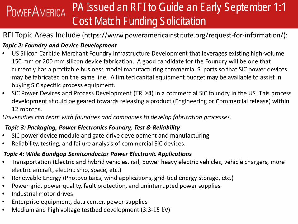
Mission SummaryPA Issued an RFI to Guide an Early September 1:1 Cost Match Funding Solicitation
Topic 2: Foundry and Device Development• US Silicon Carbide Merchant Foundry Infrastructure Development that leverages existing high-volume
150 mm or 200 mm silicon device fabrication. A good candidate for the Foundry will be one that currently has a profitable business model manufacturing commercial Si parts so that SiC power devices may be fabricated on the same line. A limited capital equipment budget may be available to assist in buying SiC specific process equipment.
• SiC Power Devices and Process Development (TRL≥4) in a commercial SiC foundry in the US. This process development should be geared towards releasing a product (Engineering or Commercial release) within 12 months.
Universities can team with foundries and companies to develop fabrication processes.Topic 3: Packaging, Power Electronics Foundry, Test & Reliability
• SiC power device module and gate-drive development and manufacturing • Reliability, testing, and failure analysis of commercial SiC devices.Topic 4: Wide Bandgap Semiconductor Power Electronic Applications• Transportation (Electric and hybrid vehicles, rail, power heavy electric vehicles, vehicle chargers, more
electric aircraft, electric ship, space, etc.)• Renewable Energy (Photovoltaics, wind applications, grid-tied energy storage, etc.)• Power grid, power quality, fault protection, and uninterrupted power supplies• Industrial motor drives• Enterprise equipment, data center, power supplies• Medium and high voltage testbed development (3.3-15 kV)
RFI Topic Areas Include (https://www.poweramericainstitute.org/request-for-information/):

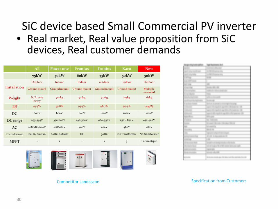
SiC device based Small Commercial PV inverter• Real market, Real value proposition from SiC
devices, Real customer demands
30
Competitor Landscape Specification from Customers
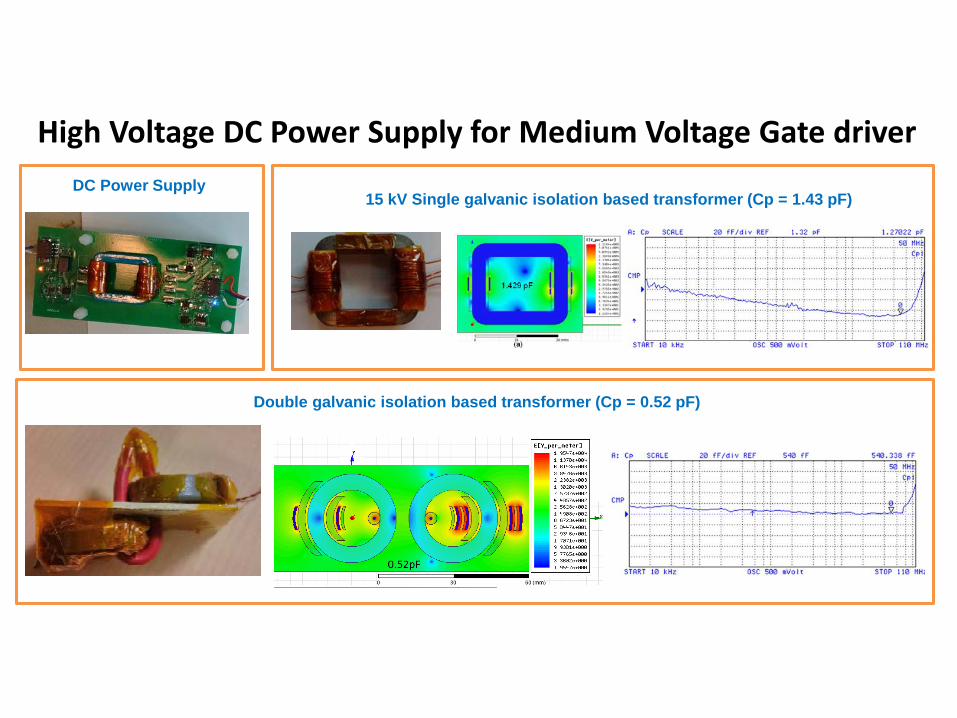
High Voltage DC Power Supply for Medium Voltage Gate driver
15 kV Single galvanic isolation based transformer (Cp = 1.43 pF)DC Power Supply
Double galvanic isolation based transformer (Cp = 0.52 pF)
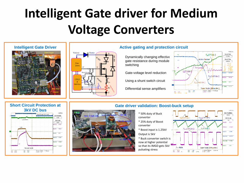
Intelligent Gate driver for Medium Voltage Converters
Active gating and protection circuit
Short Circuit Protection at 3kV DC bus
Intelligent Gate Driver (IMGD)
Dynamically changing effective gate resistance during module switching
Gate-voltage level reduction
Using a shunt switch circuit
Differential sense amplifiers
Gate driver validation: Boost-buck setup
* 50% duty of Buck converter* 25% duty of Boost converter* Boost input is 1.25kVOutput is 5kV* Buck converter switch is now at higher potential so that its IMGD gets 5kV pulsating stress