
Interplay between Roughness and Haze of CVD Grown … · Interplay between Roughness and Haze of...
13
Journal of Materials Science and Engineering B 7 (1-2) (2017) 6-18 doi: 10.17265/2161-6221/2017.1-2.002 Interplay between Roughness and Haze of CVD Grown ZnO:B Layers for a-Si:H/μc-Si:H Solar Cells Roksolana Kozak 1 and Fedor Kurdesau 2 1. Vladimir-Prelog-Weg 1-5/10, Zurich CH-8093, Switzerland 2. Oerlikon Solar Ltd., Hauptstmsse 1 A, Trubbach CH-9477, Switzerland Abstract: A broad use of ZnO:B TCO (transparent conductive oxide) layers as a front contact material for amorphous (a-Si:H) and tandem (a-Si:H/μc-Si:H) silicon thin film solar cells is achieved due to an excellent combination of good optical transparency, electrical conductivity and rough surface structure. The latter provides a light trapping effect within the underlying absorber, which is characterized by the optical haze value, i.e. a ratio between diffuse and total transmittances. The synthesis of such kind of surfaces requires the precise optimization of deposition processes, which in turn may significantly affect the further formation of silicon absorber layers and, as a result, influence the solar cells performance. Following the industrial fabrication, one has to consider both the physical properties of deposited TCO layers (resistivity, optical transparency and haze) and their processing parameters (a deposition rate, adjustable for the enterprise production tact time, and an optimum material consumption for the lowest synthesis and reactor’s cleaning costs). In the present study, the growth of ZnO:B layers by CVD (chemical vapour deposition) is discussed. The film properties and their production process characteristics were optimized in order to keep the balance between the optimum parameters of TCO layers, the best chemical conversion efficiency and the fastest deposition rate at various gas flows, pressure and temperatures. The highest attention was paid to obtain ZnO:B films with controllable optical haze, which was varied between 2 and 50% (at 600 nm wavelength) by changing the layer thickness and CVD process regimes. It was found that the crystallinity of subsequently deposited a-Si:H/μc-Si:H structures correlates with the optical haze and surface roughness of ZnO:B substrate layers, which leads to the significant effect on the light trapping and band-gap values of silicon films. Key words: TCO, thin film solar cells, optical haze, light trapping, deposition rate, material consumption. 1. Introduction The high optical transparency and good electrical conductivity of ZnO films have greatly expanded their practical application as transparent conductive electrodes in various types of photovoltaic devices [1]. It is also well known that the rough surface at the interface between the top conductive layer and light absorber stimulates the light trapping, what is particularly important for a-Si and μc-Si thin film solar cells since it compensates a low light absorption coefficient of silicon [2]. The main advantage of using ZnO films for the design of such kind of structures is a possibility to obtain any necessary texture at the interface. This goal can be achieved either by post deposition etching, when the initial smooth surface Corresponding author: Fedor Kurdesau, Dr., research fields: physics and microelectronics. produced by standard sputtering technique is modified after its fabrication by RF sputtering [3, 4], or by direct adjustment of the growth mechanism following the CVD (chemical vapour deposition) process, where the rough surface with a high diffuse transmittance can be obtained in a controllable way [4-6]. Therefore, in order to synthesize ZnO layers suitable for further application in high efficiency and low cost, Si thin film solar cells, the optimization of their CVD production parameters by tuning the optical haze, i.e. the ratio between the direct and diffusive transmittances, have to be considered [7]. In addition, the obtained rough TCO (transparent conductive oxide) surface may play a well-defined role in the growth of upper a-Si and μc-Si films. It can influence the ratio between formed amorphous and crystalline silicon phases, which is efficiently D DAVID PUBLISHING
Transcript of Interplay between Roughness and Haze of CVD Grown … · Interplay between Roughness and Haze of...
Journal of Materials Science and Engineering B 7 (1-2) (2017) 6-18 doi: 10.17265/2161-6221/2017.1-2.002
Interplay between Roughness and Haze of CVD Grown
ZnO:B Layers for a-Si:H/μc-Si:H Solar Cells
Roksolana Kozak1 and Fedor Kurdesau2
1. Vladimir-Prelog-Weg 1-5/10, Zurich CH-8093, Switzerland
2. Oerlikon Solar Ltd., Hauptstmsse 1 A, Trubbach CH-9477, Switzerland
Abstract: A broad use of ZnO:B TCO (transparent conductive oxide) layers as a front contact material for amorphous (a-Si:H) and tandem (a-Si:H/μc-Si:H) silicon thin film solar cells is achieved due to an excellent combination of good optical transparency, electrical conductivity and rough surface structure. The latter provides a light trapping effect within the underlying absorber, which is characterized by the optical haze value, i.e. a ratio between diffuse and total transmittances. The synthesis of such kind of surfaces requires the precise optimization of deposition processes, which in turn may significantly affect the further formation of silicon absorber layers and, as a result, influence the solar cells performance. Following the industrial fabrication, one has to consider both the physical properties of deposited TCO layers (resistivity, optical transparency and haze) and their processing parameters (a deposition rate, adjustable for the enterprise production tact time, and an optimum material consumption for the lowest synthesis and reactor’s cleaning costs). In the present study, the growth of ZnO:B layers by CVD (chemical vapour deposition) is discussed. The film properties and their production process characteristics were optimized in order to keep the balance between the optimum parameters of TCO layers, the best chemical conversion efficiency and the fastest deposition rate at various gas flows, pressure and temperatures. The highest attention was paid to obtain ZnO:B films with controllable optical haze, which was varied between 2 and 50% (at 600 nm wavelength) by changing the layer thickness and CVD process regimes. It was found that the crystallinity of subsequently deposited a-Si:H/μc-Si:H structures correlates with the optical haze and surface roughness of ZnO:B substrate layers, which leads to the significant effect on the light trapping and band-gap values of silicon films. Key words: TCO, thin film solar cells, optical haze, light trapping, deposition rate, material consumption.
1. Introduction
The high optical transparency and good electrical
conductivity of ZnO films have greatly expanded their
practical application as transparent conductive
electrodes in various types of photovoltaic devices [1].
It is also well known that the rough surface at the
interface between the top conductive layer and light
absorber stimulates the light trapping, what is
particularly important for a-Si and μc-Si thin film
solar cells since it compensates a low light absorption
coefficient of silicon [2]. The main advantage of using
ZnO films for the design of such kind of structures is a
possibility to obtain any necessary texture at the
interface. This goal can be achieved either by post
deposition etching, when the initial smooth surface
Corresponding author: Fedor Kurdesau, Dr., research fields: physics and microelectronics.
produced by standard sputtering technique is modified
after its fabrication by RF sputtering [3, 4], or by
direct adjustment of the growth mechanism following
the CVD (chemical vapour deposition) process, where
the rough surface with a high diffuse transmittance
can be obtained in a controllable way [4-6]. Therefore,
in order to synthesize ZnO layers suitable for further
application in high efficiency and low cost, Si thin
film solar cells, the optimization of their CVD
production parameters by tuning the optical haze, i.e.
the ratio between the direct and diffusive
transmittances, have to be considered [7].
In addition, the obtained rough TCO (transparent
conductive oxide) surface may play a well-defined
role in the growth of upper a-Si and μc-Si films. It can
influence the ratio between formed amorphous and
crystalline silicon phases, which is efficiently
D DAVID PUBLISHING
Interplay between Roughness and Haze of CVD Grown ZnO:B Layers for a-Si:H/μc-Si:H Solar Cells
7
distinguished by means of Raman measurements [8,
9]. The previous study [10] has shown a significant
dependence of Si crystallinity on the haze values
(varied by changing their thickness) of applied ZnO
precursors layers. Nevertheless, the investigation of
the above mentioned effects, in particular, the role of
the interface surface structure and the dependence of
optical haze on CVD process conditions (temperature,
pressure and gas flows) is remaining a significantly
important task. It is also crucial from the practical
point of view to take into account the industrial
production output, where other aspects, such as the
controllable deposition rate and optimum material
consumption, have to be followed in order to
minimize the fabrication and device maintaining costs
[11].
As it is known, the CVD process can be efficiently
described by two extreme cases: the surface reaction
limitation (controlled by decrease of temperature
and/or pressure) or the mass transport (gas flow)
limitation [12, 13]. The key characterization parameter
in both cases is a deposition rate. It proportionally
increases with the temperature or pressure increase in
the reaction limited regime, whereas saturates to the
maximum value in the mass transport limited
conditions, which is mainly defined by the
construction of the used chemical reactors [13].
Therefore, one of the most important CVD
characteristics for the industrial application becomes a
conversion efficiency of applied chemical reaction,
which can be calculated as a ratio between grown and
supplied materials. In the case of CVD growth of ZnO
by decomposition of DEZ (di-ethyl zinc: Zn(C2H5)2)
in water:
Zn(C2H5)2 + H2O — ZnO + C2H6 (1)
the conversion efficiency of corresponding chemical
reaction (η) can be simply found as a ratio between
the molar quantity of formed ZnO ([ZnO]) and
supplied DEZ ([DEZ]) as Eq. (2):
(2)
where vDep is a ZnO deposition rate; s is a surface area
of deposited layer, ρZnO and M(ZnO) are density and
molar mass of ZnO, respectively; Vm is a gas molar
volume at applied process conditions and VDEZ is a
DEZ supply flow.
At the optimum selection of CVD regimes, one can
obtain the highest conversion efficiency of chemical
reaction Eq. (1), which minimizes the consumption of
DEZ and, therefore, reduces the reactor contamination
outside of its deposition area, i.e. decreases cleaning
costs. Thus, the fully optimized process has to
combine the best physical properties of deposited
layers (lowest resistivity, highest optical transmittance
and haze) with the most effective growth conditions
(the highest DEZ conversion efficiency at the required
deposition rate). This paper provides a continuous
study on the importance of CVD process
optimizations for a large-scale industrial growth of
high quality ZnO:B films and their effect on
subsequently formed a-Si and μc-Si light absorber
layers.
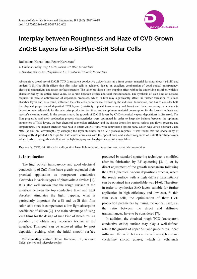
2. Experimental Details
The ZnO:B layers were synthesized by an LPCVD
(low pressure (0.5-1.5 mbar) chemical vapour
deposition) process within 174-215 oC temperature
range on TCO-1200 production set-up [14] (Oerlikon
Solar, 130 × 110 cm2 glass substrate processing area)
at 2.4-8.0 nm/s deposition rates. The H2O/DEZ
vapours mixture in 1.5-2.1 volume proportion ratio
was used as a gas precursor (see Eq. (1)), while
B2H6/hydrogen flow was applied for boron doping.
The schematic image of used LPCVD reactor is
presented in Fig. 1a. Its working performance can be
efficiently described by the characteristic curves
representing the correlation between DEZ conversion
efficiency and ZnO deposition rates. Then the linear
dependences with slopes, inversely proportional to
supplied DEZ flows, are observed, which is in a good
agreement with Eq. (2). Thus, the upper curve of Fig.
1b shows the highest possible conversion efficiency
Interplay between Roughness and Haze of CVD Grown ZnO:B Layers for a-Si:H/μc-Si:H Solar Cells
8
for the applied construction of CVD reactor (see Fig.
1a).
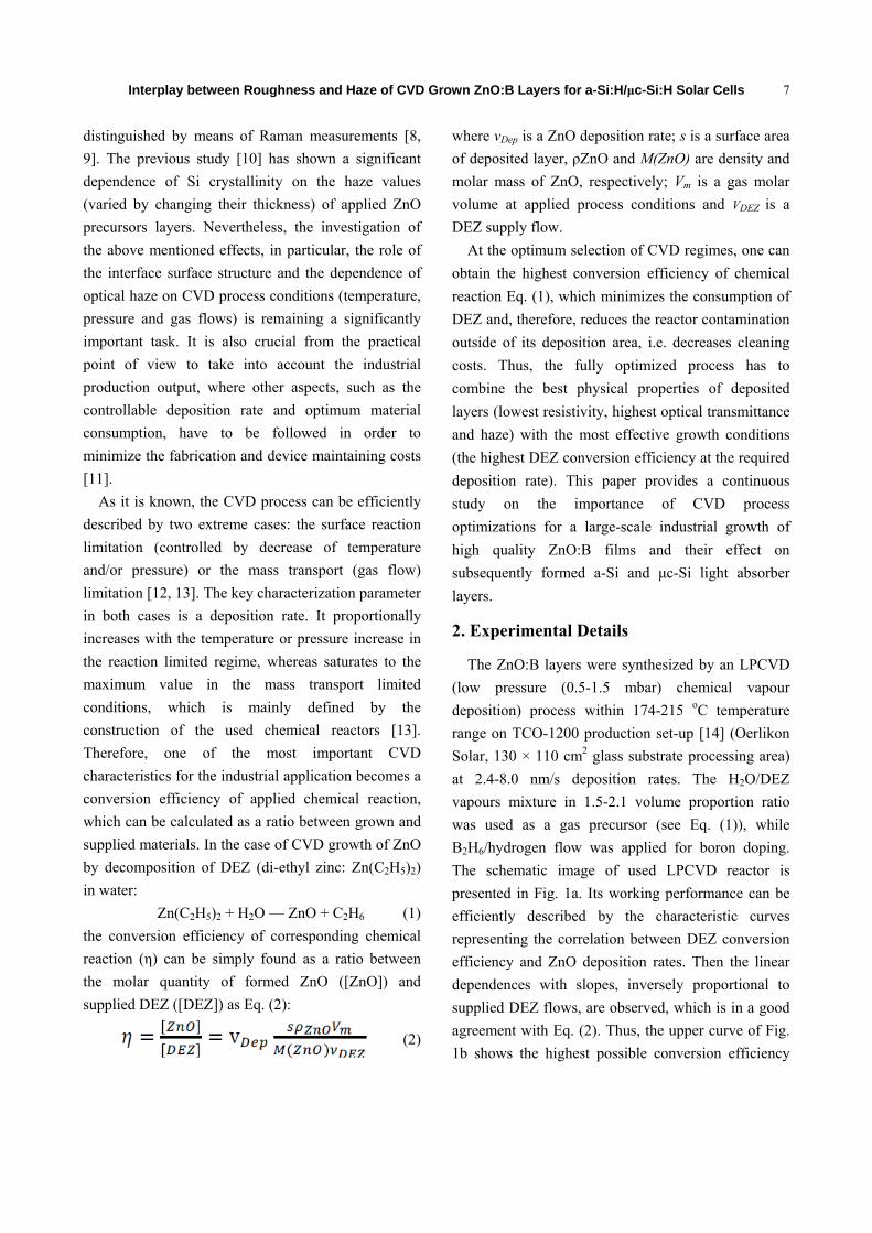
The highest attention was also paid to the optical
characterizations of deposited ZnO:B layers, where
the direct and diffuse transmittance/reflection spectra
were measured by Lambda 950 Perkin Elmer
spectrometer in the integration sphere configuration
(see Fig. 2a) under the subsequent estimation of
optical haze as a ratio between diffuse and direct
transmittances. The characteristic haze value was
selected around 600 nm and it was always followed
for the further analysis. The total absorption value for
the TCO layers was estimated from methylene iodide
(CH2I2) index matched spectra [14] as an average
within 400-800 nm (visual range) and 400-1,100 nm
(visual and infrared ranges), respectively (see Fig. 2a).
The thickness effect on the optical haze [10] can be
estimated and corrected with corresponding relative
normalized curve (see Fig. 2b). It represents the
proportion between the normalized differences of haze
and thickness comparing to values obtained from the
reference sample (i.e. 1,550 nm thick film with 15%
haze). As one can see, these changes stay almost
linear in the middle region with a proportion
coefficient close to three (Fig. 2b). Therefore, for
example, the ~60% increase in haze (from 15 to 25%)
requires ~20% thickness increase (from 1,550 to 1,900
nm).
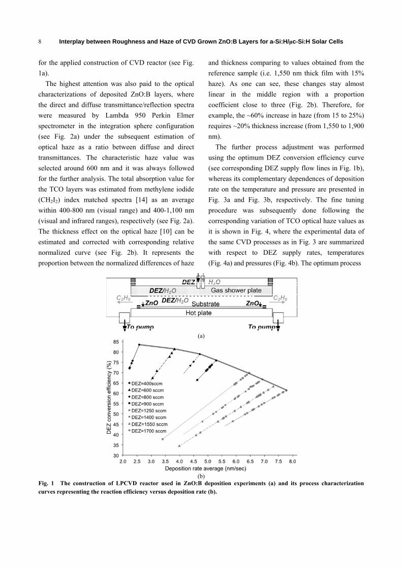
The further process adjustment was performed
using the optimum DEZ conversion efficiency curve
(see corresponding DEZ supply flow lines in Fig. 1b),
whereas its complementary dependences of deposition
rate on the temperature and pressure are presented in
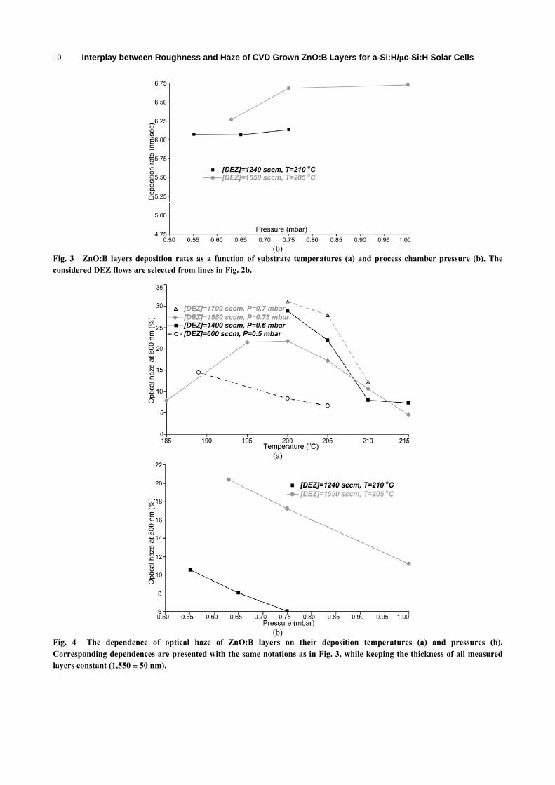
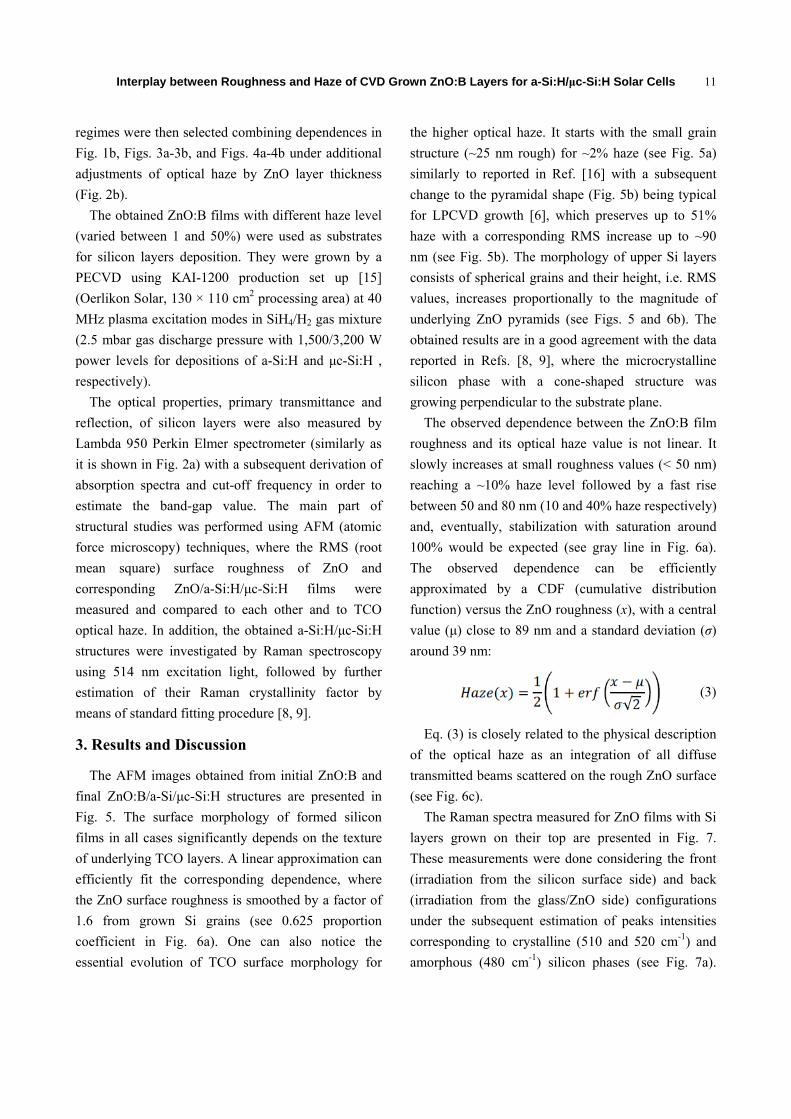
Fig. 3a and Fig. 3b, respectively. The fine tuning
procedure was subsequently done following the
corresponding variation of TCO optical haze values as
it is shown in Fig. 4, where the experimental data of
the same CVD processes as in Fig. 3 are summarized
with respect to DEZ supply rates, temperatures
(Fig. 4a) and pressures (Fig. 4b). The optimum process
(a)
(b)
Fig. 1 The construction of LPCVD reactor used in ZnO:B deposition experiments (a) and its process characterization curves representing the reaction efficiency versus deposition rate (b).
Interplay between Roughness and Haze of CVD Grown ZnO:B Layers for a-Si:H/μc-Si:H Solar Cells
9
(a)
(b)
Fig. 2 The typical optical spectrum of deposited ZnO:B layers (a) and the dependence of relative normalized changes of their optical haze at 600 nm on the corresponding film thickness varying (b). The zero point corresponds to 1,550 nm thick reference layer with 15% haze.
(a)
Interplay between Roughness and Haze of CVD Grown ZnO:B Layers for a-Si:H/μc-Si:H Solar Cells
10
(b)
Fig. 3 ZnO:B layers deposition rates as a function of substrate temperatures (a) and process chamber pressure (b). The considered DEZ flows are selected from lines in Fig. 2b.
(a)
(b)
Fig. 4 The dependence of optical haze of ZnO:B layers on their deposition temperatures (a) and pressures (b). Corresponding dependences are presented with the same notations as in Fig. 3, while keeping the thickness of all measured layers constant (1,550 ± 50 nm).
Interplay between Roughness and Haze of CVD Grown ZnO:B Layers for a-Si:H/μc-Si:H Solar Cells
11
regimes were then selected combining dependences in
Fig. 1b, Figs. 3a-3b, and Figs. 4a-4b under additional
adjustments of optical haze by ZnO layer thickness
(Fig. 2b).
The obtained ZnO:B films with different haze level
(varied between 1 and 50%) were used as substrates
for silicon layers deposition. They were grown by a
PECVD using KAI-1200 production set up [15]
(Oerlikon Solar, 130 × 110 cm2 processing area) at 40
MHz plasma excitation modes in SiH4/H2 gas mixture
(2.5 mbar gas discharge pressure with 1,500/3,200 W
power levels for depositions of a-Si:H and μc-Si:H ,
respectively).
The optical properties, primary transmittance and
reflection, of silicon layers were also measured by
Lambda 950 Perkin Elmer spectrometer (similarly as
it is shown in Fig. 2a) with a subsequent derivation of
absorption spectra and cut-off frequency in order to
estimate the band-gap value. The main part of
structural studies was performed using AFM (atomic
force microscopy) techniques, where the RMS (root
mean square) surface roughness of ZnO and
corresponding ZnO/a-Si:H/μc-Si:H films were
measured and compared to each other and to TCO
optical haze. In addition, the obtained a-Si:H/μc-Si:H
structures were investigated by Raman spectroscopy
using 514 nm excitation light, followed by further
estimation of their Raman crystallinity factor by
means of standard fitting procedure [8, 9].
3. Results and Discussion
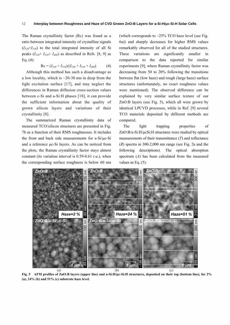
The AFM images obtained from initial ZnO:B and
final ZnO:B/a-Si/μc-Si:H structures are presented in
Fig. 5. The surface morphology of formed silicon
films in all cases significantly depends on the texture
of underlying TCO layers. A linear approximation can
efficiently fit the corresponding dependence, where
the ZnO surface roughness is smoothed by a factor of
1.6 from grown Si grains (see 0.625 proportion
coefficient in Fig. 6a). One can also notice the
essential evolution of TCO surface morphology for
the higher optical haze. It starts with the small grain
structure (~25 nm rough) for ~2% haze (see Fig. 5a)
similarly to reported in Ref. [16] with a subsequent
change to the pyramidal shape (Fig. 5b) being typical
for LPCVD growth [6], which preserves up to 51%
haze with a corresponding RMS increase up to ~90
nm (see Fig. 5b). The morphology of upper Si layers
consists of spherical grains and their height, i.e. RMS
values, increases proportionally to the magnitude of
underlying ZnO pyramids (see Figs. 5 and 6b). The
obtained results are in a good agreement with the data
reported in Refs. [8, 9], where the microcrystalline
silicon phase with a cone-shaped structure was
growing perpendicular to the substrate plane.
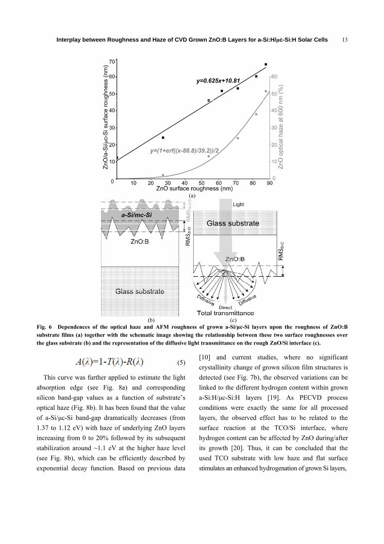
The observed dependence between the ZnO:B film
roughness and its optical haze value is not linear. It
slowly increases at small roughness values (< 50 nm)
reaching a ~10% haze level followed by a fast rise
between 50 and 80 nm (10 and 40% haze respectively)
and, eventually, stabilization with saturation around
100% would be expected (see gray line in Fig. 6a).
The observed dependence can be efficiently
approximated by a CDF (cumulative distribution
function) versus the ZnO roughness (x), with a central
value (μ) close to 89 nm and a standard deviation (σ)
around 39 nm:
(3)
Eq. (3) is closely related to the physical description
of the optical haze as an integration of all diffuse
transmitted beams scattered on the rough ZnO surface
(see Fig. 6c).
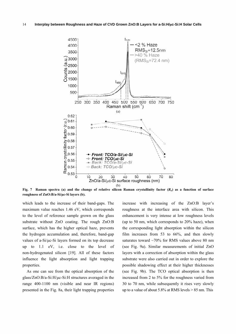
The Raman spectra measured for ZnO films with Si
layers grown on their top are presented in Fig. 7.
These measurements were done considering the front
(irradiation from the silicon surface side) and back
(irradiation from the glass/ZnO side) configurations
under the subsequent estimation of peaks intensities
corresponding to crystalline (510 and 520 cm-1) and
amorphous (480 cm-1) silicon phases (see Fig. 7a).
Interplay between Roughness and Haze of CVD Grown ZnO:B Layers for a-Si:H/μc-Si:H Solar Cells
12
The Raman crystallinity factor (Rc) was found as a
ratio between integrated intensity of crystalline signals
(I520+I510) to the total integrated intensity of all Si
peaks (I520+ I510+ I480) as described in Refs. [8, 9] as
Eq. (4):
Rc = (I520 + I510)/(I520 + I510 + I480) (4)
Although this method has such a disadvantage as
a low locality, which is ~20-30 nm in deep from the
light excitation surface [17], and may neglect the
differences in Raman diffusion cross-section values
between c-Si and a-Si:H phases [18], it can provide
the sufficient information about the quality of
grown silicon layers and variations of their
crystallinity [8].
The summarized Raman crystallinity data of
measured TCO/silicon structures are presented in Fig.
7b as a function of their RMS roughnesses. It includes
the front and back side measurements for a-Si/μc-Si
and a reference μc-Si layers. As can be noticed from
the plots, the Raman crystallinity factor stays almost
constant (its variation interval is 0.59-0.61 r.u.), when
the corresponding surface roughness is below 60 nm
(which corresponds to ~25% TCO haze level (see Fig.
6a)) and sharply decreases for higher RMS values
remarkably observed for all of the studied structures.
These variations are significantly smaller in
comparison to the data reported for similar
experiments [9], where Raman crystallinity factor was
decreasing from 50 to 20% following the transitions
between flat (low haze) and rough (large haze) surface
structures (unfortunately, no exact roughness values
were mentioned). The observed difference can be
explained by very similar surface texture of our
ZnO:B layers (see Fig. 5), which all were grown by
identical LPCVD processes, while in Ref. [9] several
TCO materials deposited by different methods are
compared.
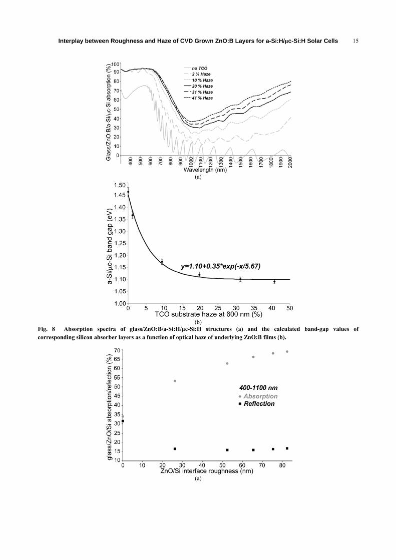
The light trapping properties of
ZnO:B/a-Si:H/μcSi:H structures were studied by optical
measurements of their transmittance (T) and reflectance
(R) spectra in 300-2,000 nm range (see Fig. 2a and the
following descriptions). The optical absorption
spectrum (A) has been calculated from the measured
values as Eq. (5):
(a) (b) (c)
Fig. 5 AFM profiles of ZnO:B layers (upper line) and a-Si:H/μc-Si:H structures, deposited on their top (bottom line), for 2% (a), 24% (b) and 51% (c) substrate haze level.
Interplay between Roughness and Haze of CVD Grown ZnO:B Layers for a-Si:H/μc-Si:H Solar Cells
13
(a)
(b) (c)
Fig. 6 Dependences of the optical haze and AFM roughness of grown a-Si/μc-Si layers upon the roughness of ZnO:B substrate films (a) together with the schematic image showing the relationship between these two surface roughnesses over the glass substrate (b) and the representation of the diffusive light transmittance on the rough ZnO/Si interface (c).
(5)
This curve was further applied to estimate the light
absorption edge (see Fig. 8a) and corresponding
silicon band-gap values as a function of substrate’s
optical haze (Fig. 8b). It has been found that the value
of a-Si/μc-Si band-gap dramatically decreases (from
1.37 to 1.12 eV) with haze of underlying ZnO layers
increasing from 0 to 20% followed by its subsequent
stabilization around ~1.1 eV at the higher haze level
(see Fig. 8b), which can be efficiently described by
exponential decay function. Based on previous data
[10] and current studies, where no significant
crystallinity change of grown silicon film structures is
detected (see Fig. 7b), the observed variations can be
linked to the different hydrogen content within grown
a-Si:H/μc-Si:H layers [19]. As PECVD process
conditions were exactly the same for all processed
layers, the observed effect has to be related to the
surface reaction at the TCO/Si interface, where
hydrogen content can be affected by ZnO during/after
its growth [20]. Thus, it can be concluded that the
used TCO substrate with low haze and flat surface
stimulates an enhanced hydrogenation of grown Si layers,
Interplay between Roughness and Haze of CVD Grown ZnO:B Layers for a-Si:H/μc-Si:H Solar Cells
14
(a)
(b)
Fig. 7 Raman spectra (a) and the change of relative silicon Raman crystallinity factor (Ro) as a function of surface roughness of ZnO:B/a-Si/μc-Si layers (b).
which leads to the increase of their band-gaps. The
maximum value reaches 1.46 eV, which corresponds
to the level of reference sample grown on the glass
substrate without ZnO coating. The rough ZnO:B
surface, which has the higher optical haze, prevents
the hydrogen accumulation and, therefore, band-gap
values of a-Si/μc-Si layers formed on its top decrease
up to 1.1 eV, i.e. close to the level of
non-hydrogenated silicon [19]. All of these factors
influence the light absorption and light trapping
properties.
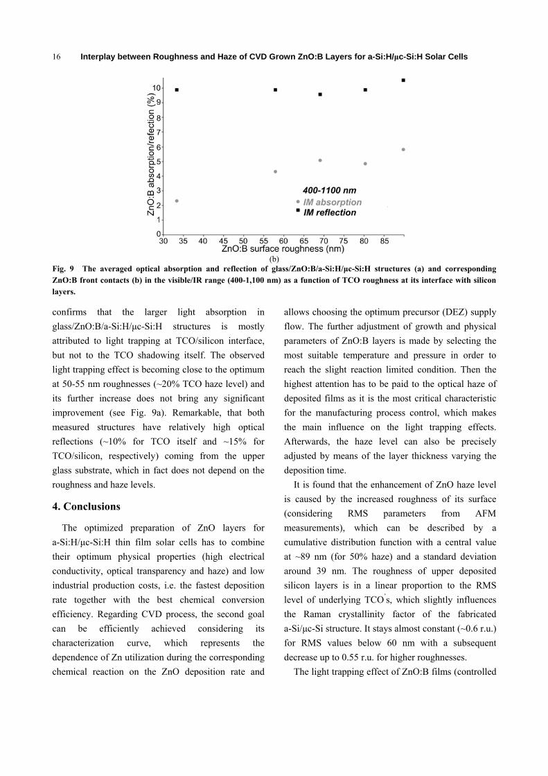
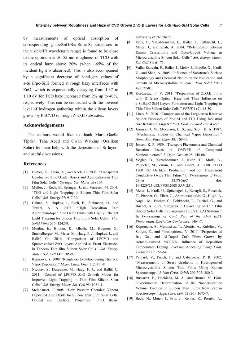
As one can see from the optical absorption of the
glass/ZnO:B/a-Si:H/μc-Si:H structures averaged in the
range 400-1100 nm (visible and near IR regions)
presented in the Fig. 8a, their light trapping properties
increase with increasing of the ZnO:B layer’s
roughness at the interface area with silicon. This
enhancement is very intense at low roughness levels
(up to 50 nm, which corresponds to 20% haze), when
the corresponding light absorption within the silicon
film increases from 53 to 66%, and then slowly
saturates toward ~70% for RMS values above 80 nm
(see Fig. 9a). Similar measurements of initial ZnO
layers with a correction of absorption within the glass
substrate were also carried out in order to explore the
possible shadowing effect at their higher thicknesses
(see Fig. 9b). The TCO optical absorption is then
increased from 2 to 5% for the roughness varied from
30 to 70 nm, while subsequently it rises very slowly
up to a value of about 5.8% at RMS levels > 85 nm. This
Interplay between Roughness and Haze of CVD Grown ZnO:B Layers for a-Si:H/μc-Si:H Solar Cells
15
(a)
(b)
Fig. 8 Absorption spectra of glass/ZnO:B/a-Si:H/μc-Si:H structures (a) and the calculated band-gap values of corresponding silicon absorber layers as a function of optical haze of underlying ZnO:B films (b).
(a)
Interplay between Roughness and Haze of CVD Grown ZnO:B Layers for a-Si:H/μc-Si:H Solar Cells
16
(b)
Fig. 9 The averaged optical absorption and reflection of glass/ZnO:B/a-Si:H/μc-Si:H structures (a) and corresponding ZnO:B front contacts (b) in the visible/IR range (400-1,100 nm) as a function of TCO roughness at its interface with silicon layers.
confirms that the larger light absorption in
glass/ZnO:B/a-Si:H/μc-Si:H structures is mostly
attributed to light trapping at TCO/silicon interface,
but not to the TCO shadowing itself. The observed
light trapping effect is becoming close to the optimum
at 50-55 nm roughnesses (~20% TCO haze level) and
its further increase does not bring any significant
improvement (see Fig. 9a). Remarkable, that both
measured structures have relatively high optical
reflections (~10% for TCO itself and ~15% for
TCO/silicon, respectively) coming from the upper
glass substrate, which in fact does not depend on the
roughness and haze levels.
4. Conclusions
The optimized preparation of ZnO layers for
a-Si:H/μc-Si:H thin film solar cells has to combine
their optimum physical properties (high electrical
conductivity, optical transparency and haze) and low
industrial production costs, i.e. the fastest deposition
rate together with the best chemical conversion
efficiency. Regarding CVD process, the second goal
can be efficiently achieved considering its
characterization curve, which represents the
dependence of Zn utilization during the corresponding
chemical reaction on the ZnO deposition rate and
allows choosing the optimum precursor (DEZ) supply
flow. The further adjustment of growth and physical
parameters of ZnO:B layers is made by selecting the
most suitable temperature and pressure in order to
reach the slight reaction limited condition. Then the
highest attention has to be paid to the optical haze of
deposited films as it is the most critical characteristic
for the manufacturing process control, which makes
the main influence on the light trapping effects.
Afterwards, the haze level can also be precisely
adjusted by means of the layer thickness varying the
deposition time.
It is found that the enhancement of ZnO haze level
is caused by the increased roughness of its surface
(considering RMS parameters from AFM
measurements), which can be described by a
cumulative distribution function with a central value
at ~89 nm (for 50% haze) and a standard deviation
around 39 nm. The roughness of upper deposited
silicon layers is in a linear proportion to the RMS
level of underlying TCO’s, which slightly influences
the Raman crystallinity factor of the fabricated
a-Si/μc-Si structure. It stays almost constant (~0.6 r.u.)
for RMS values below 60 nm with a subsequent
decrease up to 0.55 r.u. for higher roughnesses.
The light trapping effect of ZnO:B films (controlled
Interplay between Roughness and Haze of CVD Grown ZnO:B Layers for a-Si:H/μc-Si:H Solar Cells
17
by measurements of optical absorption of
corresponding glass/ZnO:B/a-Si/μc-Si structures in
the visible/IR wavelength range) is found to be close
to the optimum at 50-55 nm roughness of TCO with
its optical haze above 20% (when ~65% of the
incident light is absorbed). This is also accompanied
by a significant decrease of band-gap values of
a-Si:H/μc-Si:H formed at rough hazy interfaces with
ZnO, which is exponentially decaying from 1.37 to
1.10 eV for TCO haze increased from 2% up to 40%,
respectively. This can be connected with the lowered
level of hydrogen gathering within the silicon layers
grown by PECVD on rough ZnO:B substrates.
Acknowledgements
The authors would like to thank Maria-Gaelle
Tipaka, Taha Abed and Owan Watkins (Oerlikon
Solar) for their help with the deposition of Si layers
and useful discussions.
References
[1] Ellmer, K., Klein, A., and Rech, B. 2008. “Transparent Conductive Zinc Oxide: Basics and Applications in Thin Film Solar Cells.” Springer Ser. Mater. Sci 104.
[2] Muller, J., Rech, B., Springer, J., and Vanecek, M. 2004. “TCO and Light Trapping in Silicon Thin Film Solar Cells.” Sol. Energy 77: 917-30.
[3] Calnan, S., Hupkes, J., Rech, B., Siekmann, H., and Tiwari, A. N. 2008. “High Deposition Rate Aluminum-doped Zinc Oxide Films with Highly Efficient Light Trapping for Silicon Thin Films Solar Cells.” Thin Solid Films 516: 1242-8.
[4] Moulin, E., Bittkau, K., Ghosh, M., Bugnon, G., Stuckelberger, M., Meier, M., Haug, F. J., Hupkes, J., and Ballif, Ch. 2016. “Comparison of LPCVD and Sputter-etched ZnO Layers Applied as Front Electrodes in Tandem Thin-film Silicon Solar Cells.” Sol. Energy Mater. Sol. Cell 145: 185-97.
[5] Kajakawa, Y. 2008. “Roughness Evolution during Chemical Vapor Deposition.” Mater. Chem. Phys. 112: 311-8.
[6] Nicolay, S., Despeisse, M., Haug, F. J., and Ballif, C. 2011. “Control of LPCVD ZnO Growth Modes for Improved Light Trapping in Thin Film Silicon Solar Cells.” Sol. Energy Mater. Sol. Cell 95: 1031-4.
[7] Steinhauser, J. 2008. “Low Pressure Chemical Vapour Deposited Zinc Oxide for Silicon Thin Film Solar Cells. Optical and Electrical Properties.” Ph.D. thesis,
University of Neuchatel. [8] Droz, C., Vallat-Sauvain, E., Bailat, J., Feitknecht, L.,
Meier, J., and Shah, A. 2004. “Relationship between Raman Crystallinity and Open-Circuit Voltage in Microcrystalline Silicon Solar Cells.” Sol. Energy Mater. Sol. Cell 81: 61-71.
[9] Vallat-Sauvain, E., Bailat, J., Meier, J., Niquile, X., Kroll, U., and Shah, A. 2005. “Influence of Substrate’s Surface Morphology and Chemical Nature on the Nucleation and Growth of Microcrystalline Silicon.” Thin Solid Films 485: 77-81.
[10] Kurdzesau, F. V. 2011. “Preparation of ZnO:B Films with Different Optical Haze and Their Influence on a-Si:H/μC-Si:H Layers Formation and Light Trapping in Thin Film Silicon Solar Cells.” PFMT 4 (9): 45-50.
[11] Linss, V. 2016. “Comparison of the Large-Area Reactive Sputter Processes of Zno:Al and ITO Using Industrial Size Rotatable Targets.” Surf. Coat. Technol 290: 43-57.
[12] Jasinski, J. M., Meyerson, B. S., and Scott, B. A. 1987. “Mechanistic Studies of Chemical Vapor Deposition.” Annu. Rev. Phys. Chem 38: 109-40.
[13] Jensen, K. F. 1989. “Transport Phenomena and Chemical Reaction Issues in OMVPE of Compound Semiconductors.” J. Cryst. Growth 98: 148-66.
[14] Vogler, B., Kerschbaumer, J., Kuhn, H., Mark, A., Poppeler, M., Zimin, D., and Zindel, A. 2008. “TCO 1200 OC Oerlikon Production Tool for Transparent Conductive Oxide Thin Films.” In Proceedings of Proc. 23-rd EUPVSEC. doi: 10.4229/23rdEUPVSE2008-3AV.251.
[15] Meier, J., Kroll, U., Spitznagel, J., Benagli, S., Roschek, T., Pfanner, G., Ellert, C., Androutsopoulos, G., Hugli, A., Nagel, M., Bucher, C., Feitknecht, L., Buchel, G., and Buchel, A. 2005. “Progress in Up-scaling of Thin Film Silicon Solar Cells by Large-area PECVD KAI Systems.” In Proceedings of Conf. Rec. of the 31-st IEEE Photovoltaic Specialists Conference, 1464-7.
[16] Kuprenaite, S., Murauskas, T., Abrutis, A., Kubilius, V., Saltyte, Z., and Plausinaitiene, V. 2015. “Properties of In-, Ga-, and Al-Doped ZnO Films Grown by Aerosol-assisted MOCVD: Influence of Deposition Temperature, Doping Level and Annealing.” Surf. Coat. Technol 271: 156-64.
[17] Paillard, V., Puech, P., and Cabarrocas, P. R. 2002.
“Measurements of Stress Gradients in Hydrogenated
Microcrystalline Silicon Thin Films Using Raman
Spectroscopy.” J. Non-Cryst. Solids 299-302: 280-3.
[18] Bustarret, E., Hachicha, M. A., and Brunel, M. 1988.
“Experimental Determination of the Nanocrystalline
Volume Fraction in Silicon Thin Films from Raman
Spectroscopy.” Appl. Phys. Lett. 52 (20): 1675-7.
[19] Beck, N., Meier, J., Fric, J., Remes, Z., Poruba, A.,

Interplay between Roughness and Haze of CVD Grown ZnO:B Layers for a-Si:H/μc-Si:H Solar Cells
18
Fluckiger, R., Pohl, J., Shah, A., and Vanecek, M. 1996. “Enhanced Optical Absorption in Microcrystalline Silicon.” J. Non-Cryst. Solids 198-200: 903-6.
[20] Wang, F. H., Chang, H. P., Tseng, Ch. Ch., and Huang,
Ch. Ch. 2011. “Effects of H2 Plasma Treatment on Properties of Zno:Al Thin Films Prepared by RF Magnetron Sputtering.” Surf. Coat. Technol 205: 5269-77.

![The Navier wall law at a boundary with random roughness · 2017-03-01 · arXiv:0711.3610v1 [math.AP] 22 Nov 2007 The Navier wall law at a boundary with random roughness David G´erard-Varet](https://static.fdocument.org/doc/165x107/5eb9bde442992d36c26b76b7/the-navier-wall-law-at-a-boundary-with-random-roughness-2017-03-01-arxiv07113610v1.jpg)


![Electronic Supplementary Information Magnesium β ... · 1 Electronic Supplementary Information Magnesium β-Ketoiminates as CVD Precursors for MgO Formation Elaheh Pousaneh[a], Tobias](https://static.fdocument.org/doc/165x107/60651f68f5d4f347af3c4c60/electronic-supplementary-information-magnesium-1-electronic-supplementary.jpg)