Introductioncsmantech.org/OldSite/Digests/2016/Paper 10a 3... · Web viewannealed at 775 oC for 1...
6
Keywords: AlGaN, III-nitride, ohmic contact Abstract We report a study of Vanadium (V)-based ohmic contact on Al-rich n-AlGaN films using the transfer length measurement (TLM) and x-ray photoemission spectroscopy. The V-based ohmic contact shows lower contact resistance, smoother surface morphology, and lower annealing temperature when compared to the Ti-based ohmic contact. With the formation of the nitrogen-vanadium bond after the thermal annealing, the N:1s core-level peak at the V-Al 0.55 Ga 0.45 N interface was shifted by 0.7 eV toward the higher binding energy. The interface states help the surface pinning of the Fermi level that further facilitates the current conduction for the n-type AlGaN ohmic contact. The data demonstrated that the use of V as the first layer of the n-type ohmic contact for Al-rich n-AlGaN could be a better choice of ohmic contact metal than the conventional Ti/Al-based ohmic contact. INTRODUCTION Since the first demonstration of high efficiency blue light emitting diodes (LEDs), the development of ultraviolet (UV and deep-ultraviolet (DUV) LEDs had led to rapid commercializations of these devices in various lighting applications. With the growing interest in nitride semiconductor emitters and detectors operating at DUV wavelengths, suitable ohmic contact for Al-rich n-AlGaN materials would be highly desired. In general, AlGaN has a work function of less than 4.0 eV. There would be a need to find appropriate methods to form an ohmic contact with intermediate transition layers. The issue of forming low-resistivity ohmic contact Al-rich AlGaN layers was also challenging with the increase of the dopant’s activation energy as the aluminium composition increases. The commonly reported ohmic contact systems for n-AlGaN are Titanium (Ti)- based metallization schemes since TiN has a work function of 3.74 eV and it could be formed at the interface after the annealing process. Miller et al. reported the ohmic contact on n-Al x Ga 1-x N (x = 0.58) can be achieved after the sample was annealed at 900-1000 o C under the nitrogen ambient, yielding a specific contact resistance (ρ c ) of 4.0×10 -4 -1.7×10 - 3 Ω-cm 2 [ 1 ]. However, the high-temperature annealing process is typically undesired as the ohmic contact morphology would become rough after high-temperature annealing process. There are also concerns of the device process integration compatibility as well as potential device reliability in lieu of the high-temperature process. Vanadium (V)-based ohmic contact could be a suitable choice for Al-rich n-AlGaN because thermally stable nitride complex T.-T. Kao*, Y.-S. Liu, T. Detchprohm, R. D. Dupuis, and S.-C. Shen School of Electrical and Computer Engineering, Georgia Institute of Technology, 777 Atlantic Drive NW, Atlanta, GA, 30332-0250 *e-mail: [email protected] Phone: 404-385-8327 Vanadium-based Ohmic Contact for Aluminum-rich n-AlGaN
-
Upload
duonghuong -
Category
Documents
-
view
220 -
download
1
Transcript of Introductioncsmantech.org/OldSite/Digests/2016/Paper 10a 3... · Web viewannealed at 775 oC for 1...
Keywords: AlGaN, III-nitride, ohmic contact
AbstractWe report a study of Vanadium (V)-based ohmic
contact on Al-rich n-AlGaN films using the transfer length measurement (TLM) and x-ray photoemission spectroscopy. The V-based ohmic contact shows lower contact resistance, smoother surface morphology, and lower annealing temperature when compared to the Ti-based ohmic contact. With the formation of the nitrogen-vanadium bond after the thermal annealing, the N:1s core-level peak at the V-Al0.55Ga0.45N interface was shifted by 0.7 eV toward the higher binding energy. The interface states help the surface pinning of the Fermi level that further facilitates the current conduction for the n-type AlGaN ohmic contact. The data demonstrated that the use of V as the first layer of the n-type ohmic contact for Al-rich n-AlGaN could be a better choice of ohmic contact metal than the conventional Ti/Al-based ohmic contact.
INTRODUCTION
Since the first demonstration of high efficiency blue light emitting diodes (LEDs), the development of ultraviolet (UV and deep-ultraviolet (DUV) LEDs had led to rapid commercializations of these devices in various lighting applications. With the growing interest in nitride semiconductor emitters and detectors operating at DUV wavelengths, suitable ohmic contact for Al-rich n-AlGaN materials would be highly desired. In general, AlGaN has a work function of less than 4.0 eV. There would be a need to find appropriate methods to form an ohmic contact with intermediate transition layers. The issue of forming low-resistivity ohmic contact Al-rich AlGaN layers was also challenging with the increase of the dopant’s activation energy as the aluminium composition increases.
The commonly reported ohmic contact systems for n-AlGaN are Titanium (Ti)-based metallization schemes since TiN has a work function of 3.74 eV and it could be formed at the interface after the annealing process. Miller et al. reported the ohmic contact on n-AlxGa1-xN (x = 0.58) can be achieved after the sample was annealed at 900-1000 oC under the nitrogen ambient, yielding a specific contact resistance (ρc) of 4.0×10⁻⁴-1.7×10⁻³ Ω-cm2 [1]. However, the high-temperature annealing process is typically undesired as the ohmic contact morphology would become rough after high-temperature
annealing process. There are also concerns of the device process integration compatibility as well as potential device reliability in lieu of the high-temperature process. Vanadium (V)-based ohmic contact could be a suitable choice for Al-rich n-AlGaN because thermally stable nitride complex can be created at the metal-III-N interface using low temperature annealing processes [2-5].
In this paper, we report a study of the V-based ohmic contact properties on AlGaN films for various Al compositions. We studied the evolution of the contact resistance as a function of the annealing temperature and the material bonding characteristics at the V-AlGaN interface using an x-ray photoemission spectroscopy (XPS) measurement. When compared to the Ti-based contact, V-based ohmic contact consistently shows lower ρc and smoother surface morphology at lower annealing temperature for n-type AlxGa1-xN films (x up to 0.55.) A study of the N:1s core-level peak at V-Al0.55Ga0.45N interface shows that the formation of nitrogen-vanadium (N-V) bond helps shift the peak binding energy by 0.7 eV at the V-AlGaN interface when compared to annealed Ti-AlGaN interface. The increase in the binding energy facilitates the current conduction by providing more effective electron states for carrier transport at the metal-semiconductor interface. The results indicated that the use of V-based ohmic contact is a suitable choice of achieving low contact resistance for n-AlGaN layers.
DEVICE STRUCTURES AND FABRICATION PROCESSING
The n-type AlxGa1-xN films (x = 0.06, 0.49, 0.55, 0.6, and 0.73) were grown on c-plane sapphire substrates by a Thomas Swan metal-organic chemical vapor deposition (MOCVD) system. In this study, the Al0.06Ga0.94N film was grown on a 2.5 μm-thick GaN buffer layer and its thickness is 250 nm. Other Al-rich AlxGa1-xN films (x = 0.49, 0.55, 0.6, and 0.73) were 200 nm thick and they were grown on a 1 μm-thick AlN buffer layer. V/Al/Ti/Au and Ti/Al/Ti/Au stacks were deposited on each of the AlGaN samples for contact study.
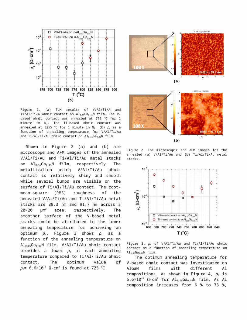
RESULTS AND DISCUSSIONSShown in Figure 1 (a) is the comparison of transmission
line method (TLM) results for V-based and Ti-based ohmic contact on Al0.55Ga0.45N films. The V-based ohmic contact was annealed at 775 oC for 1 minute in N2 and Ti-based ohmic contact was annealed at 825 oC for 1 minute in N2. By
T.-T. Kao*, Y.-S. Liu, T. Detchprohm, R. D. Dupuis, and S.-C. Shen
School of Electrical and Computer Engineering, Georgia Institute of Technology, 777 Atlantic Drive NW, Atlanta, GA, 30332-0250
*e-mail: [email protected] Phone: 404-385-8327
Vanadium-based Ohmic Contact for Aluminum-rich n-AlGaN
Microsoft Office User, 04/08/16,
Jansen: Fix centering, shifted during publications edits
Microsoft Office User, 04/08/16,
Jansen: This should be on top on it’s own line (see CS ManTech formatting template)
Microsoft Office User, 04/08/16,
Jansen: Fix centering, shifted during publications edits
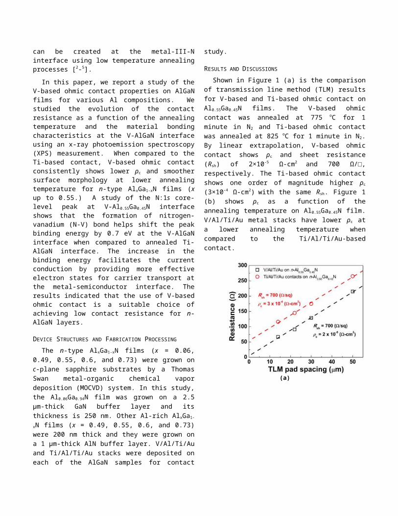
linear extrapolation, V-based ohmic contact shows ρc and sheet resistance (Rsh) of 2×10⁻⁵ Ω-cm2 and 700 Ω/, respectively. The Ti-based ohmic contact shows one order of magnitude higher ρc (3×10⁻⁴ Ω-cm2) with the same Rsh. Figure1 (b) shows ρc as a function of the annealing temperature on Al0.55Ga0.45N film. V/Al/Ti/Au metal stacks have lower ρc at a lower annealing temperature when compared to the Ti/Al/Ti/Au-based contact.
(a)
(b)
Figure 1. (a) TLM results of V/Al/Ti/A and Ti/Al/Ti/A ohmic contact on Al0.55Ga0.45N film. The V-based ohmic contact was annealed at 775 oC for 1 minute in N2. The Ti-based ohmic contact was annealed at 8255 oC for 1 minute in N2. (b) ρc as a function of annealing temperature for V/Al/Ti/Au and Ti/Al/Ti/Au ohmic contact on Al0.55Ga0.45N film.
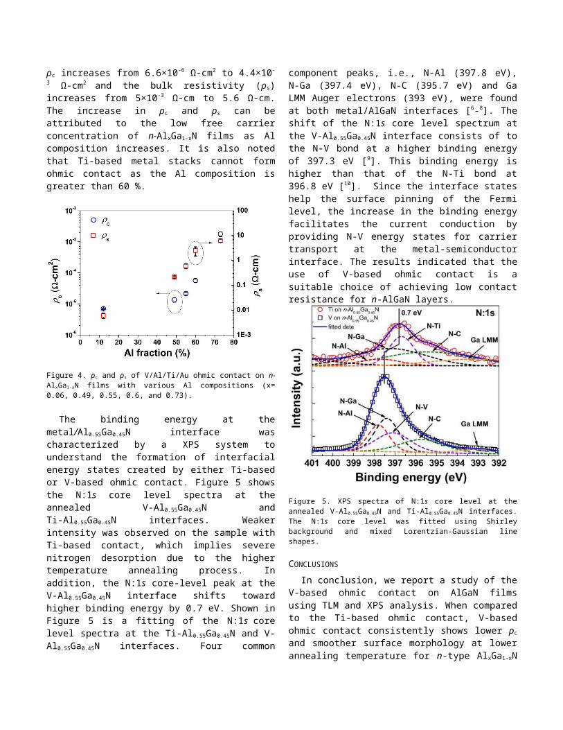
Shown in Figure 2 (a) and (b) are microscope and AFM images of the annealed V/Al/Ti/Au and Ti/Al/Ti/Au metal stacks on Al0.55Ga0.45N film, respectively. The metallization using V/Al/Ti/Au ohmic contact is relatively shiny and smooth while several bumps are visible on the surface of Ti/Al/Ti/Au contact. The root-mean-square (RMS) roughness of the annealed V/Al/Ti/Au and Ti/Al/Ti/Au metal stacks are 38.3 nm and 91.7 nm across a 20×20 µm2 area, respectively.
The smoother surface of the V-based metal stacks could be attributed to the lower annealing temperature for achieving an optimum ρc. Figure 3 shows ρc as a function of the annealing temperature on Al0.06Ga0.88N film. V/Al/Ti/Au ohmic contact provides a lower ρc at each annealing temperature compared to Ti/Al/Ti/Au ohmic contact. The optimum value of ρc= 6.6×10⁻⁶ Ω-cm2 is found at 725 oC.
100 X
(a)
100 X
(b)
Figure 2. The microscopic and AFM images for the annealed (a) V/Al/Ti/Au and (b) Ti/Al/Ti/Au metal stacks.
Figure 3. ρc of V/Al/Ti/Au and Ti/Al/Ti/Au ohmic contact as a function of annealing temperature on Al0.06Ga0.88N film.
The optimum annealing temperature for V-based ohmic contact was investigated on AlGaN films with different Al
compositions. As shown in Figure 4, ρc is 6.6×10⁻⁶ Ω-cm2 for Al0.06Ga0.94N film. As Al composition increases from 6 % to 73 %, ρc increases from 6.6×10⁻⁶ Ω-cm2 to 4.4×10⁻³ Ω-cm2 and the bulk resistivity (ρs) increases from 5×10⁻³ Ω-cm to 5.6 Ω-cm. The increase in ρc and ρs can be attributed to the low free carrier concentration of n-AlxGa1-xN films as Al composition increases. It is also noted that Ti-based metal stacks cannot form ohmic contact as the Al composition is greater than 60 %.
Figure 4. ρc and ρs of V/Al/Ti/Au ohmic contact on n-AlxGa1-xN films with various Al compositions (x= 0.06, 0.49, 0.55, 0.6, and 0.73).
The binding energy at the metal/Al0.55Ga0.45N interface was characterized by a XPS system to understand the formation of interfacial energy states created by either Ti-based or V-based ohmic contact. Figure 5 shows the N:1s core level spectra at the annealed V-Al0.55Ga0.45N and Ti-Al0.55Ga0.45N interfaces. Weaker intensity was observed on the sample with Ti-based contact, which implies severe nitrogen desorption due to the higher temperature annealing process. In addition, the N:1s core-level peak at the V-Al0.55Ga0.45N interface shifts toward higher binding energy by 0.7 eV. Shown in Figure 5 is a fitting of the N:1s core level spectra at the Ti-Al0.55Ga0.45N and V-Al0.55Ga0.45N interfaces. Four common component peaks, i.e., N-Al (397.8 eV), N-Ga (397.4 eV), N-C (395.7 eV) and Ga LMM Auger electrons (393 eV), were found at both metal/AlGaN interfaces [6-8]. The shift of the N:1s core level spectrum at the V-Al0.55Ga0.45N interface consists of to the N-V bond at a higher binding energy of 397.3 eV [9]. This binding energy is higher than that of the N-Ti bond at 396.8 eV [10]. Since the interface states help the surface pinning of the Fermi level, the increase in the binding energy facilitates the current conduction by providing N-V energy states for carrier transport at the metal-semiconductor interface. The results indicated that the use of V-based ohmic contact is a suitable choice of achieving low contact resistance for n-AlGaN layers.
Figure 5. XPS spectra of N:1s core level at the annealed V-Al0.55Ga0.45N and Ti-Al0.55Ga0.45N interfaces. The N:1s core level was fitted using Shirley background and mixed Lorentzian-Gaussian line shapes.
CONCLUSIONS
In conclusion, we report a study of the V-based ohmic contact on AlGaN films using TLM and XPS analysis. When compared to the Ti-based ohmic contact, V-based ohmic contact consistently shows lower ρc and smoother surface morphology at lower annealing temperature for n-type AlxGa1-xN films (x up to 0.55). A study of the N:1s core-level peak at V-Al0.55Ga0.45N interface shows that the formation of N-V bond helps shift the peak binding energy by 0.7 eV at the V-AlGaN interface when compared to the annealed Ti-AlGaN interface. The increase in the binding energy facilitates the current conduction by providing more effective energy states for carrier transport at the metal-semiconductor interface. As a result, using V-based contact helps achieve low annealing temperature requirement (< 800 oC) that leads to better surface morphology than conventional Ti-based ohmic contact.
ACKNOWLEDGEMENTS
The authors are thankful for the cleanroom facility support of the staff in the Microelectronic Research Center at the Georgia Institute of Technology in Atlanta, GA. This work is supported by the Defense Advanced Research Projects Agency under Contract #W911NF-15-1-0026.
REFERENCES
Microsoft Office User, 04/08/16,
Jansen: Remove line under Reference and 2nd line that is now on top of the next page
1 [] M. A. Miller, B. H. Koo, K. H. A. Bogart, and S. E. Mohney, “Ti/Al/Ti/Au and V/Al/V/Au Contact to Plasma-Etched n-Al0.58Ga0.42N,” J. Electron. Mater., vol. 37, pp. 564, Sep. 2008.
2 [] V. S. Fomenko, “Handbook of Thermionic Properties: Electronic Work Functions and Richardson Constants of Elements and Compounds,” (Plenum, New York, 1966).
5 [] R. France, T. Xu, P. Chen, R. Chandrasekaran, and T. D. Moustakas, “Vanadium-based Ohmic contact to n-AlGaN in the entire alloy composition,” Appl. Phys. Lett., vol. 90, pp. 062115, 2007.
6 [] P. Y. Jouan, M. C. Peignon, Ch. Cardinaud, G. Lempérière, “Characterization of TiN coatings and of the TiN/Si interface by X-ray photoelectron spectroscopy and Auger electron spectroscopy,” Appl. Surf. Sci., vol. 68, pp. 595-603, Aug. 1993.
8 [] K. Li, A.T.S. Wee, J. Lin, Z. C. Feng and S. J. Chua, “X-ray Photoelectron Spectroscopy Evaluation on Surface Chemical States of GaN, InGaN and AlGaN Heteroepitaxial Thin Films Grown on Sapphire by MOCVD,” Mat. Res. Soc. Symp. Proc., vol. 618, pp. 303, 2000.
9 [] P. K. Barhai, N. Kumari, I. Banerjee, S. K. Pabi, S. K. Mahapatra, “Study of the effect of plasma current density on the formation of titanium nitride and titanium oxynitride thin films prepared by reactive DC magnetron sputtering,” Vacuum, vol. 84, pp. 896-901, 2010.
10 []I. Galesic, B.O. Kolbesen, “Formation of vanadium nitride by rapid thermal processing,” Thin Solid Films, vol. 349, pp. 14-18, 1999.
DUV: deep-ultravioletTLM: Transfer length measurementXPS: X-ray photoemission spectroscopyLED: Light emitting diodeTi: TitaniumV: VanadiumMOCVD: metal-organic chemical vapor depositionρc: specific contact resistanceρs: bulk resistivityICP: inductively coupled plasmaRsh: sheet resistanceRMS: root-mean-square