HO#2 MOS Physics - Harvard John A. Paulson School of...
32
T. H. Lee Handout #2: EE214 Fall 2001 A Review of MOS Device Physics1996 Thomas H. Lee, rev. September 26, 2001; All rights reserved Page 1 of 32 A Review of MOS Device Physics 1.0 Introduction This set of notes focuses on those aspects of transistor behavior that are of immediate rel- evance to the analog circuit designer. Separation of first order from higher order phenom- ena is emphasized, so there are many instances when crude approximations are presented in the interest of developing insight. As a consequence, this review is intended as a supple- ment to, rather than a replacement of, traditional rigorous treatments of the subject. 2.0 A Little History Attempts to create field-effect transistors actually predate the development of bipolar devices by over twenty years. In fact, the first patent application for a FET-like transistor was by Julius Lilienfeld in 1925, but he never constructed a working device. Before co- inventing the bipolar transistor, William Shockley also tried to modulate the conductivity of a semiconductor to create a field-effect transistor. Like Lilienfeld, problems with his materials system, copper compounds 1 , prevented success. Even after moving on to germa- nium (a much simpler – and therefore much more easily understood – semiconductor than copper oxide), Shockley was still unable to make a working FET. In the course of trying to understand the reasons for the spectacular lack of success, Shockley’s Bell Laboratories colleagues John Bardeen and Walter Brattain stumbled across the point-contact bipolar transistor, the first practical semiconductor amplifier. Unresolved mysteries with that device (such as negative β, among others) led Shockley to invent the junction transistor, and the three eventually won a Nobel Prize in physics for their work. 3.0 FETs: The Short Story Although the quantitative details are a bit complicated, the basic idea that underlies the operation of a FET is simple: Start with a resistor and add a third terminal (the gate) that somehow allows modulation of the resistance between the other two terminals (the source and drain). If the power expended in driving the control terminal is less than that delivered to a load, power gain results. In a junction FET (see Figure 1), a reverse-biased PN junction controls the resistance between the source and drain terminals. Because the width of a depletion layer depends on bias, a gate voltage variation alters the effective cross-sectional area of the device, thereby 1. Rectifiers made of cuprous oxide had been in use since the 1920’s, even though the detailed operating principles were not understood. Around 1976, with decades of semiconductor research to support him, Shockley took one last shot at making a copper oxide FET (at Stanford). Still unsuccessful, he despaired of ever knowing why. (See the July, 1976 issue of the Transactions on Electron Devices for Shockley’s remi- niscences and other fascinating stories.)
Transcript of HO#2 MOS Physics - Harvard John A. Paulson School of...
T. H. Lee Handout #2: EE214 Fall 2001
A Review of MOS Device Physics
1996 Thomas H. Lee, rev. September 26, 2001; All rights reserved Page 1 of 32
A Review of MOS Device Physics
1.0 Introduction
This set of notes focuses on those aspects of transistor behavior that are of immediate rel-evance to the analog circuit designer. Separation of first order from higher order phenom-ena is emphasized, so there are many instances when crude approximations are presented in the interest of developing insight. As a consequence, this review is intended as a supple-ment to, rather than a replacement of, traditional rigorous treatments of the subject.
2.0 A Little History
Attempts to create field-effect transistors actually predate the development of bipolar devices by over twenty years. In fact, the first patent application for a FET-like transistor was by Julius Lilienfeld in 1925, but he never constructed a working device. Before co-inventing the bipolar transistor, William Shockley also tried to modulate the conductivity of a semiconductor to create a field-effect transistor. Like Lilienfeld, problems with his materials system, copper compounds
1
, prevented success. Even after moving on to germa-nium (a much simpler – and therefore much more easily understood – semiconductor than copper oxide), Shockley was still unable to make a working FET. In the course of trying to understand the reasons for the spectacular lack of success, Shockley’s Bell Laboratories colleagues John Bardeen and Walter Brattain stumbled across the point-contact bipolar transistor, the first practical semiconductor amplifier. Unresolved mysteries with that device (such as negative
β
, among others) led Shockley to invent the junction transistor, and the three eventually won a Nobel Prize in physics for their work.
3.0 FETs: The Short Story
Although the quantitative details are a bit complicated, the basic idea that underlies the operation of a FET is simple: Start with a resistor and add a third terminal (the gate) that somehow allows modulation of the resistance between the other two terminals (the source and drain). If the power expended in driving the control terminal is less than that delivered to a load, power gain results.
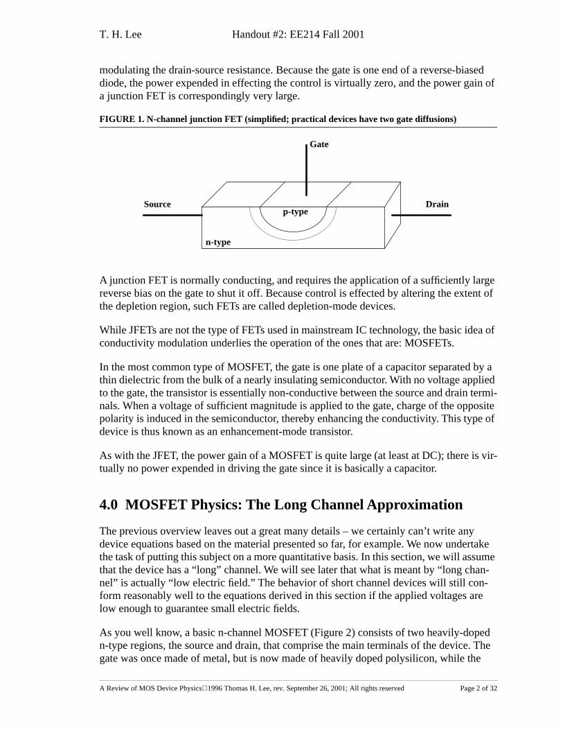
In a junction FET (see Figure 1), a reverse-biased PN junction controls the resistance between the source and drain terminals. Because the width of a depletion layer depends on bias, a gate voltage variation alters the effective cross-sectional area of the device, thereby
1. Rectifiers made of cuprous oxide had been in use since the 1920’s, even though the detailed operating principles were not understood. Around 1976, with decades of semiconductor research to support him, Shockley took one last shot at making a copper oxide FET (at Stanford). Still unsuccessful, he despaired of ever knowing why. (See the July, 1976 issue of
the
Transactions on Electron Devices
for Shockley’s remi-niscences and other fascinating stories.)
T. H. Lee Handout #2: EE214 Fall 2001
A Review of MOS Device Physics
1996 Thomas H. Lee, rev. September 26, 2001; All rights reserved Page 2 of 32
modulating the drain-source resistance. Because the gate is one end of a reverse-biased diode, the power expended in effecting the control is virtually zero, and the power gain of a junction FET is correspondingly very large.
FIGURE 1. N-channel junction FET (simplified; practical devices have two gate diffusions)
A junction FET is normally conducting, and requires the application of a sufficiently large reverse bias on the gate to shut it off. Because control is effected by altering the extent of the depletion region, such FETs are called depletion-mode devices.
While JFETs are not the type of FETs used in mainstream IC technology, the basic idea of conductivity modulation underlies the operation of the ones that are: MOSFETs.
In the most common type of MOSFET, the gate is one plate of a capacitor separated by a thin dielectric from the bulk of a nearly insulating semiconductor. With no voltage applied to the gate, the transistor is essentially non-conductive between the source and drain termi-nals. When a voltage of sufficient magnitude is applied to the gate, charge of the opposite polarity is induced in the semiconductor, thereby enhancing the conductivity. This type of device is thus known as an enhancement-mode transistor.
As with the JFET, the power gain of a MOSFET is quite large (at least at DC); there is vir-tually no power expended in driving the gate since it is basically a capacitor.
4.0 MOSFET Physics: The Long Channel Approximation
The previous overview leaves out a great many details – we certainly can’t write any device equations based on the material presented so far, for example. We now undertake the task of putting this subject on a more quantitative basis. In this section, we will assume that the device has a “long” channel. We will see later that what is meant by “long chan-nel” is actually “low electric field.” The behavior of short channel devices will still con-form reasonably well to the equations derived in this section if the applied voltages are low enough to guarantee small electric fields.
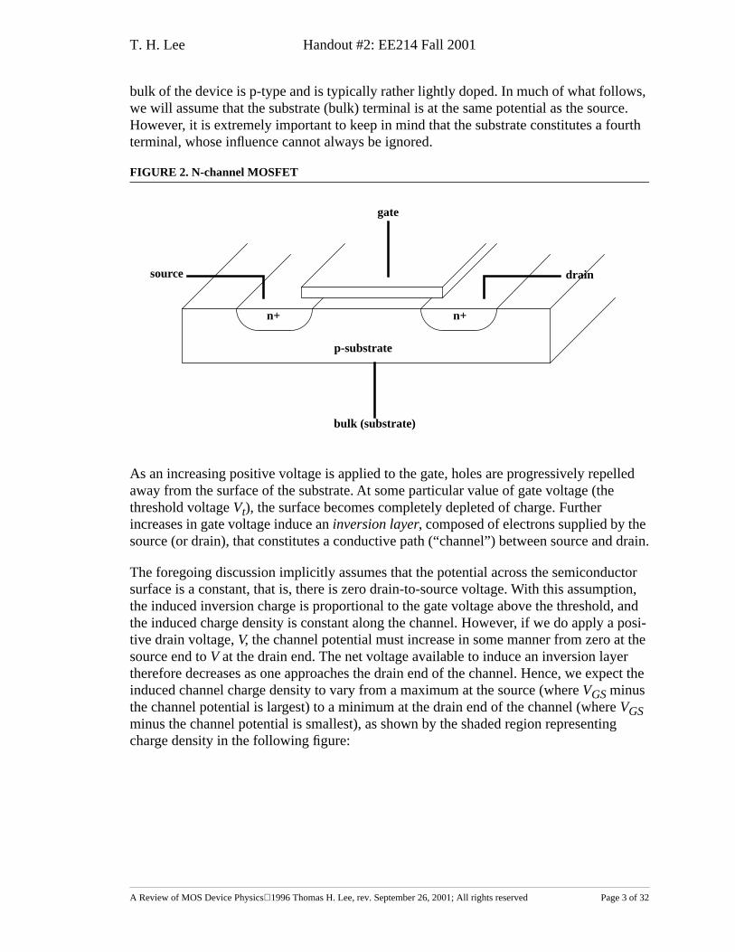
As you well know, a basic n-channel MOSFET (Figure 2) consists of two heavily-doped n-type regions, the source and drain, that comprise the main terminals of the device. The gate was once made of metal, but is now made of heavily doped polysilicon, while the
Gate
Source Drainp-type
n-type
T. H. Lee Handout #2: EE214 Fall 2001
A Review of MOS Device Physics
1996 Thomas H. Lee, rev. September 26, 2001; All rights reserved Page 3 of 32
bulk of the device is p-type and is typically rather lightly doped. In much of what follows, we will assume that the substrate (bulk) terminal is at the same potential as the source. However, it is extremely important to keep in mind that the substrate constitutes a fourth terminal, whose influence cannot always be ignored.
FIGURE 2. N-channel MOSFET
As an increasing positive voltage is applied to the gate, holes are progressively repelled away from the surface of the substrate. At some particular value of gate voltage (the threshold voltage
V
t
), the surface becomes completely depleted of charge. Further increases in gate voltage induce an
inversion layer
, composed of electrons supplied by the source (or drain), that constitutes a conductive path (“channel”) between source and drain.
The foregoing discussion implicitly assumes that the potential across the semiconductor surface is a constant, that is, there is zero drain-to-source voltage. With this assumption, the induced inversion charge is proportional to the gate voltage above the threshold, and the induced charge density is constant along the channel. However, if we do apply a posi-tive drain voltage,
V
, the channel potential must increase in some manner from zero at the source end to
V
at the drain end. The net voltage available to induce an inversion layer therefore decreases as one approaches the drain end of the channel. Hence, we expect the induced channel charge density to vary from a maximum at the source (where
V
GS
minus the channel potential is largest) to a minimum at the drain end of the channel (where
V
GS
minus the channel potential is smallest), as shown by the shaded region representing charge density in the following figure:
p-substrate
n+ n+
gate
drainsource
bulk (substrate)
T. H. Lee Handout #2: EE214 Fall 2001
A Review of MOS Device Physics
1996 Thomas H. Lee, rev. September 26, 2001; All rights reserved Page 4 of 32
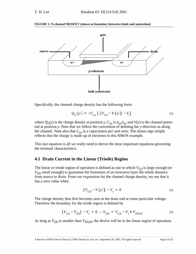
FIGURE 3. N-channel MOSFET (shown at boundary between triode and saturation)
Specifically, the channel charge density has the following form:
(1)
where
Q
n
(
y
) is the charge density at position
y
,
C
ox
is
ε
ox
/t
ox
and
V
(
y
)
is the channel poten-tial at position
y
. Note that we follow the convention of defining the
y
-direction as along the channel. Note also that
C
ox
is a capacitance
per unit area
. The minus sign simply reflects that the charge is made up of electrons in this NMOS example.
This last equation is all we really need to derive the most important equations governing the terminal characteristics.
4.1 Drain Current in the Linear (Triode) Region
The linear or triode region of operation is defined as one in which
V
GS
is large enough (or
V
DS
small enough) to guarantee the formation of an inversion layer the whole distance from source to drain. From our expression for the channel charge density, we see that it has a zero value when
(2)
The charge density thus first becomes zero at the drain end at some particular voltage. Therefore the boundary for the triode region is defined by
(3)
As long as
V
DS
is smaller than
V
DSAT
, the device will be in the linear region of operation.
p-substrate
n+ n+
gate
drainsource
bulk (substrate)
Qn y( ) Cox VGS V y( )−[ ] Vt−{ }−=
VGS V y( )−[ ] Vt− 0=
VGS VDS−[ ] Vt− 0 VDS→ VGS Vt VDSAT≡−= =
T. H. Lee Handout #2: EE214 Fall 2001
A Review of MOS Device Physics
1996 Thomas H. Lee, rev. September 26, 2001; All rights reserved Page 5 of 32
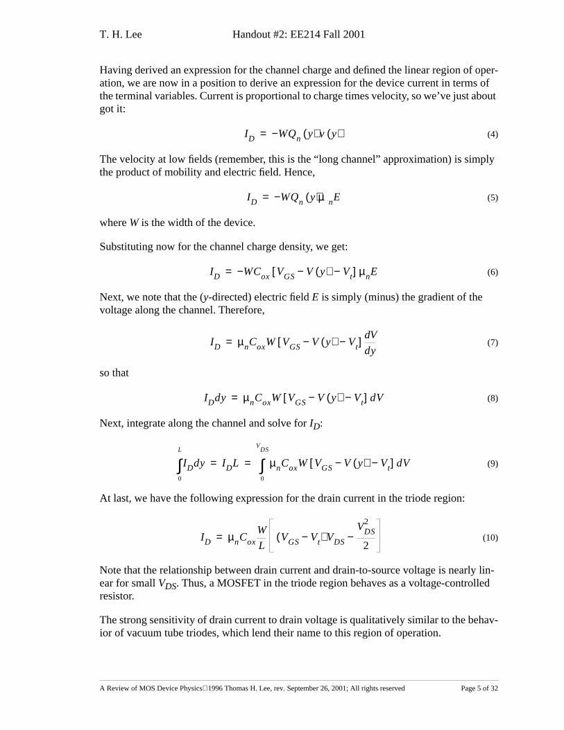
Having derived an expression for the channel charge and defined the linear region of oper-ation, we are now in a position to derive an expression for the device current in terms of the terminal variables. Current is proportional to charge times velocity, so we’ve just about got it:
(4)
The velocity at low fields (remember, this is the “long channel” approximation) is simply the product of mobility and electric field. Hence,
(5)
where
W
is the width of the device.
Substituting now for the channel charge density, we get:
(6)
Next, we note that the (
y
-directed) electric field
E
is simply (minus) the gradient of the voltage along the channel. Therefore,
(7)
so that
(8)
Next, integrate along the channel and solve for
I
D
:
(9)
At last, we have the following expression for the drain current in the triode region:
(10)
Note that the relationship between drain current and drain-to-source voltage is nearly lin-ear for small
V
DS
. Thus, a MOSFET in the triode region behaves as a voltage-controlled resistor.
The strong sensitivity of drain current to drain voltage is qualitatively similar to the behav-ior of vacuum tube triodes, which lend their name to this region of operation.
ID WQn y( ) v y( )−=
ID WQn y( ) µnE−=
ID W− Cox VGS V y( )− Vt−[ ] µ nE=
ID µnCoxW VGS V y( )− Vt−[ ]yd
dV=
IDdy µnCoxW VGS V y( )− Vt−[ ] dV=
IDdy0
L
∫ IDL µnCoxW VGS V y( )− Vt−[ ] dV0
VDS
∫= =
ID µnCoxW
LVGS Vt−( ) VDS
VDS2
2−=
T. H. Lee Handout #2: EE214 Fall 2001
A Review of MOS Device Physics
1996 Thomas H. Lee, rev. September 26, 2001; All rights reserved Page 6 of 32
4.2 Drain Current in Saturation
When
V
DS
is high enough so that the inversion layer does not extend all the way from source to drain, the channel is said to be “pinched off.” In this case, the channel charge ceases to increase, causing the total current to remain constant despite increases in
V
DS
.
Calculating the value of this current is easy; all we have to do is substitute
V
DSAT
for
V
DS
in our expression for current:
(11)
which simplifies to:
(12)
Hence, in saturation, the drain current has a square-law dependence on the gate-source voltage, and is (ideally) independent of drain voltage. Because vacuum tube pentodes exhibit a similar insensitivity of plate current to plate voltage, this regime is occasionally called the pentode region of operation.
The transconductance of such a device in saturation is easily found from differentiating our expression for drain current:
(13)
which may also be expressed as:
(14)
Thus, in contrast with bipolar devices, a long-channel MOSFET’s transconductance depends only on the square-root of the bias current.
4.3 Channel-Length Modulation
So far, we’ve assumed that the drain current is independent of drain-source voltage in sat-uration. However, measurements on real devices always show a disappointing lack of such independence. The primary mechanism responsible for a nonzero output conductance in long channel devices is channel-length modulation (CLM). Since the drain region forms a junction with the substrate, there is a depletion region surrounding the drain whose extent depends on the drain voltage. As the drain voltage increases, the depletion zone’s width increases as well, effectively shortening the channel. Since the effective length thus decreases, the drain current increases.
ID µnCoxW
LVGS Vt−( ) VDSAT
VDSAT2
2−=
ID
µnCox
2
W
LVGS Vt−( ) 2=
gm µnCoxW
LVGS Vt−( )=
gm 2µnCoxW
LID=
T. H. Lee Handout #2: EE214 Fall 2001
A Review of MOS Device Physics
1996 Thomas H. Lee, rev. September 26, 2001; All rights reserved Page 7 of 32
To account for this effect, the drain current equations for both triode and saturation are modified as follows:
(15)
where
i
D0
is the drain current when channel-length modulation is ignored, and the param-eter
λ
is a semi-empirical constant whose dimensions are those of inverse voltage. The reciprocal of
λ
is often given the symbol
V
A
and called the Early voltage, after the fellow who first explained nonzero output conductance in bipolar transistors (where it is caused by an analogous modulation of base width with collector voltage). The graphical signifi-cance of the Early voltage is that it is the common extrapolated zero current intercept of the
i
D
–
v
DS
device curves.
4.4 Dynamic Elements
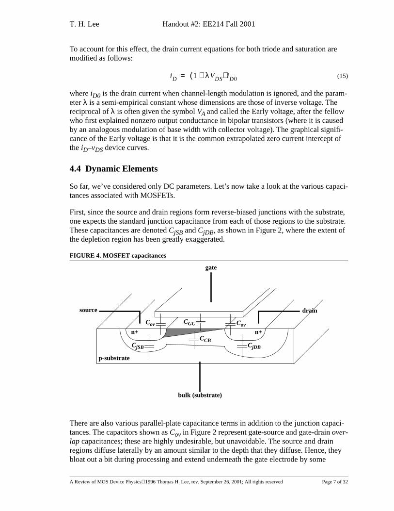
So far, we’ve considered only DC parameters. Let’s now take a look at the various capaci-tances associated with MOSFETs.
First, since the source and drain regions form reverse-biased junctions with the substrate, one expects the standard junction capacitance from each of those regions to the substrate. These capacitances are denoted
C
jSB
and
C
jDB
, as shown in Figure 2, where the extent of the depletion region has been greatly exaggerated.
FIGURE 4. MOSFET capacitances
There are also various parallel-plate capacitance terms in addition to the junction capaci-tances. The capacitors shown as
C
ov
in Figure 2 represent gate-source and gate-drain
over-lap
capacitances; these are highly undesirable, but unavoidable. The source and drain regions diffuse laterally by an amount similar to the depth that they diffuse. Hence, they bloat out a bit during processing and extend underneath the gate electrode by some
iD 1 λVDS+( ) iD0=
gate
drainsource
n+ n+
p-substrate
CjSB CjDB
CovCov CGC
CCB
bulk (substrate)
T. H. Lee Handout #2: EE214 Fall 2001
A Review of MOS Device Physics
1996 Thomas H. Lee, rev. September 26, 2001; All rights reserved Page 8 of 32
amount. As a crude approximation, one may take the amount of overlap,
L
D
, as 2/3 to 3/4 of the depth of the source/drain diffusions. Hence,
(16)
where
x
j
is the depth of the source-drain diffusions,
ε
ox
is the oxide’s dielectric constant (about 3.9
ε
0
), and
t
ox
is the oxide thickness.
The parallel-plate overlap terms are augmented by fringing and thus the “overlap” capaci-tance would be nonzero even in the absence of actual overlap. In this context, one should keep in mind that, in modern devices, the gate electrode is actually thicker than the chan-nel is long, so the relative dimensions of Figure 2 are misleading. In fact, since the thick-ness of the gate electrode scales little (if at all), the “overlap” capacitance now changes somewhat slowly from generation to generation.
Another parallel-plate capacitance is the gate-to-channel capacitance,
C
GC
. Since both the source and drain regions extend into the region underneath the gate, the effective channel length decreases by twice the bloat,
L
D
. Hence, the total value of
C
GC
is
(17)
There is also a capacitance between the channel and the bulk
, C
CB
, that behaves as a junc-tion capacitance as well. Its value is approximately:
(18)
where
x
d
is the depth of the depletion layer, whose value is given by:
(19)
The quantity in the absolute value symbol is the difference between the surface potential and the Fermi level in the substrate. In the triode and saturation regions, this quantity has a magnitude of twice the Fermi level.
Now, the channel is not a terminal of the device, so to find how the various capacitive terms contribute to the terminal capacitances requires knowledge of how the channel charge divides between the source and drain. In general, the values of the terminal capaci-tances depend on the operating regime because bias conditions affect this partitioning of charge. For example, when there is
no
inversion charge (the device is “off”), the gate-source and gate-drain capacitances are just the overlap terms to a good approximation.
Cov
εox
tox
WLD≈ 0.7CoxWxj=
CGC CoxW L 2LD−( )=
CCB
εSi
xd
W L 2LD−( )=
xd
2εSi
qNsub
φs φF−=
T. H. Lee Handout #2: EE214 Fall 2001
A Review of MOS Device Physics
1996 Thomas H. Lee, rev. September 26, 2001; All rights reserved Page 9 of 32
When the device is in the linear region, there is an inversion layer, and one may assume that the source and drain share the channel charge equally. Hence, half of
C
GC
adds to the overlap terms.
Similarly, the
C
jSB
and
C
jDB
junction terms are each augmented by one-half of
C
CB
in the linear region.
In the saturation region, potential variations at the drain region don’t influence the channel charge. Hence, there is no contribution to
C
GD
by
C
GC
; the overlap term is all there is. The gate-source capacitance
is
affected by
C
GC
, but “detailed considerations”
2
show that only about 2/3 of
C
GC
should be added to the overlap term.
Similarly,
C
CB
contributes nothing to
C
DB
in saturation, but does contribute 2/3 of its value to
C
SB
.
The gate-bulk capacitance may be taken as zero in both triode and saturation (the channel charge essentially shields the bulk from what’s happening at the gate). When the device is off, however, there is a gate-voltage dependent capacitance whose value varies in a roughly linear manner between
C
GC
and the series combination of
C
GC
and
C
CB
. Below, but near, threshold, the value is closer to the series combination, and approaches a limiting value of
C
GC
in deep accumulation, where the surface majority carrier concentration increases owing to the positive charge induced by the strong negative gate bias. In deep accumulation, the surface is strongly conducting, and may therefore be treated as essen-tially a metal, leading to a gate-bulk capacitance that is the full parallel-plate value.
The variation of this capacitance with bias presents one additional option for realizing var-actors. To avoid the need for negative supply voltages, the capacitor may be built in an n-well using n+ source and drain regions.
The terminal capacitances are summarized in the following table:
2. The 2/3 factor arises from the calculation of channel charge, and inherently comes from integrating the triangular distribution assumed in Figure 2 in the square-law regime.
TABLE 1. Approximate MOSFET terminal capacitances
Off Triode Saturation
C
GS
C
OV
C
GC
/2 +
C
OV
2
C
GC
/3 +
C
OV
C
GD
C
OV
C
GC
/2 +
C
OV
C
OV
C
GB
C
GC
C
CB
/(
C
GC
+
C
CB
) <
C
GB
<
C
GC
0 0
T. H. Lee Handout #2: EE214 Fall 2001
A Review of MOS Device Physics
1996 Thomas H. Lee, rev. September 26, 2001; All rights reserved Page 10 of 32
4.5 High-Frequency Figures of Merit
It is perhaps natural to attempt to characterize multidimensional quantities with a single number; laziness is universal, after all. In the specific case of high-frequency performance, two figures of merit are particularly popular. These are
ω
T
and
ω
max
, which are the fre-quencies at which the current and power gain, respectively, are extrapolated to fall to unity. It is worthwhile to review briefly their derivation since many engineers forget the origins and precise meanings of these quantities, and often draw incorrect inferences as a result.
The most common expression for
ω
T
assumes that the drain is terminated in an incremen-tal short circuit, while the gate is driven by an ideal current source. As a consequence of the shorted termination,
ω
T
does not include information about drain-bulk capacitance. The current-source drive implies that series gate resistance similarly has no influence on
ω
T
. Clearly, both
r
g
and
C
gd
can have a strong effect on high-frequency performance, but
ω
T
simply ignores this reality.
Furthermore, the gate-to-drain capacitance is considered only in the computation of the input impedance; its feedforward contribution to output current is neglected. With these assumptions, the ratio of drain current to gate current is
(20)
which has a unity value at a frequency
(21)
Now, the frequency at which the (extrapolated) current gain goes to unity has no funda-mental importance; it is simply easy to compute. Perhaps more relevant is the frequency at which the maximum power gain is extrapolated to fall to unity. To compute
ω
max
in gen-eral is quite difficult, however, so we will invoke several simplifying assumptions to make an approximate derivation possible. Specifically, we compute the input impedance with an incrementally shorted drain, and ignore the feedforward current through
C
gd
, just as in the computation of
ω
T
. We do consider the feed
back
from drain to gate through
C
gd
in com-
C
SB
C
jSB
C
jSB
+
C
CB
/2
C
jSB
+ 2
C
CB
/3
C
DB
C
jDB
C
jDB
+
C
CB
/2
C
jDB
TABLE 1. Approximate MOSFET terminal capacitances
Off Triode Saturation
iD
iin
gm
ω Cgs Cgd+( )≈
ωT
gm
Cgs Cgd+=
T. H. Lee Handout #2: EE214 Fall 2001
A Review of MOS Device Physics
1996 Thomas H. Lee, rev. September 26, 2001; All rights reserved Page 11 of 32
puting the output impedance, however, which is important because computation of the maximum power gain requires termination in a conjugate match.
With these assumptions, we can calculate the power delivered to the input by the current source drive as simply
(22)
where
r
g
, the series gate resistance, is the only dissipative element in the input circuit.
The magnitude of the short-circuit current gain at high frequencies is approximately given by the same expression used in the computation of
ω
T
:
(23)
It is also straightforward to show that the resistive part of the output impedance is roughly
(24)
If the conjugate termination has a conductance of this value, the power gain will be maxi-mized, with half of the
g
m
generator’s current going into the conductance of the termina-tion, and the balance into the device itself. The total maximum power gain is therefore
(25)
which has a unity value at a frequency given by
(26)
It is clear that
ω
max
depends on the gate resistance, so it is more comprehensive in this regard than
ω
T
. Because judicious layout can reduce gate resistance to small values,
ω
max
can be considerably larger than
ω
T
for many MOSFETs. The output capacitance has no effect on
ω
max
because it can be tuned out with a pure inductance, and therefore does not limit the amount of power that may be delivered to a load.
Pin
iin2 rg
2=
iD
iin
ωT
ω≈
gout gm
Cgd
Cgd Cgs+⋅≈ ωT Cgd⋅=
PL
Pin
1
2
ωT
ωiin
1
2⋅ ⋅
2
1
ωT Cgd⋅( )
iin2 rg
2
ωT
ω24rgCgd
≈ ≈
ωmax1
2
ωT
rgCgd
≈
T. H. Lee Handout #2: EE214 Fall 2001
A Review of MOS Device Physics
1996 Thomas H. Lee, rev. September 26, 2001; All rights reserved Page 12 of 32
Measurements of both
ω
max
and
ω
T
are carried out by increasing the frequency until a noticeable drop in maximum power gain or current gain occurs. A simple extrapolation to unity value then yields
ω
max
and
ω
T
. Because these are extrapolated values, it is not neces-sarily a given that one may actually construct practical circuits operating at, say,
ω
max
. These figures of merit should instead be taken as rough indications of high frequency per-formance capability.
4.6 Technology Scaling in the Long-Channel Limit
Now that we have examined both the static and dynamic behavior of MOSFETs, we can derive an approximate expression for
ω
T
in terms of operating point, process parameters and device geometry. We’ve already derived an expression for
g
m
, so all we need is an expression for the requisite capacitances. To simplify the derivation, let us assume that
C
GS
dominates the input capacitance, and is itself dominated by the parallel-plate capaci-tance. Then, in saturation:
(27)
Hence,
ω
T
depends on the inverse square of the length, and increases with increasing gate-source voltage. Remember, though, that this equation holds only in the long-channel regime.
5.0 Operation in Weak Inversion (Subthreshold)
In simple MOSFET models (such as the one we’ve presented so far), the device conducts no current until an inversion layer forms. However, mobile carriers don’t abruptly disap-pear the moment the gate voltage drops below
V
t
. In fact, exercising a little imagination, one can discern a structure reminiscent of an NPN bipolar transistor when the device is in the subthreshold regime, with the source and drain regions functioning as emitter and col-lector, respectively, and the (non-inverted) bulk behaving a bit like a base.
As
V
GS
drops below threshold, the current decreases in an exponential fashion, much like a bipolar transistor. Rather than dropping at the 60mV/decade rate of a bipolar, however, the current in all real MOSFETs drops more slowly (e.g., 100mV/decade) because of the capacitive voltage division between gate-source and source-bulk.
The equations of the Level 2 and Level 3 SPICE models illustrate one specific way to accommodate subthreshold effects quantitatively. Strictly speaking, understanding this information is not necessary for EE214 (i.e., you will never be tested on this material), but this information is presented in the belief that knowing more is better than knowing less.
ωT
gm
Cgs
µnCoxW
LVGS Vt−( )
2
3WLCox
≈ ≈ 3
2
µn VGS Vt−( )
L2=
T. H. Lee Handout #2: EE214 Fall 2001
A Review of MOS Device Physics
1996 Thomas H. Lee, rev. September 26, 2001; All rights reserved Page 13 of 32
5.1 Background
The development so far has assumed that the MOSFET operates in strong inversion. Recall that this condition is defined as a degree of inversion such that the density of charge carriers induced at the surface is at least as great as the (oppositely charged) mobile carrier density in the bulk. This inversion charge is then assumed to drift from source to drain under the influence of a lateral field. In fact, we have implicitly assumed so far that carrier transport is
entirely
by drift. Furthermore we have simply stated, without explanation, that strong inversion corresponds to values of gate overdrives of at least “several”
kT
/
q
. We now consider device behavior in weak inversion (a term we will use interchangeably with subthreshold), where gate overdrives do not satisfy this requirement, and we also quantify what is meant by “several.”
To extend our analysis into the weak inversion regime, first acknowledge that the mobile carrier density at the surface does not drop abruptly to zero as the gate voltage diminishes. However, because the carrier density will be low, the contribution to drain current by drift will be small. We therefore need to consider the real possibility that current transport by
diffusion
may also be important in this operating regime. This acknowledgment is the key to understanding operation in weak inversion.
Before presenting any equations, it’s useful to examine a couple of
I
-
V
plots in order to develop a feel for the phenomena we are trying to describe mathematically. For example, a plot of the square-root of drain current vs. gate-source voltage ought to be a simple straight line, if we believe in the Level 1 equations. However, real devices behave differ-ently:
FIGURE 5.
I
-
V
plot for a “more real” MOSFET (
V
DS
>
V
DSsat
)
One noteworthy feature of this plot is that the current does not drop to zero below thresh-old. Rather it tails off in some manner, and the region where it does is what we are calling the weak inversion regime.
3
Beyond some amount above threshold, the current is propor-tional to the square of the overdrive (as predicted by Level 1 equations); we call this region the square-law regime. At very high overdrives, the dependence of drain current on
3. It is by no means required that the drain current go to zero at zero
V
GS
, by the way.
VGS
ID
VT
T. H. Lee Handout #2: EE214 Fall 2001
A Review of MOS Device Physics
1996 Thomas H. Lee, rev. September 26, 2001; All rights reserved Page 14 of 32
overdrive becomes sub-quadratic, owing to various high-field effects (both lateral and ver-tical).
From this plot, we see that the threshold voltage is perhaps most naturally defined as the
extrapolated
zero-current intercept of the linear portion of the curve above threshold.
Additional insights result if we present the same data on a semilog plot:
FIGURE 6. Semilog
I
-
V
plot for a “more real” MOSFET (
V
DS
>
V
DSsat
)
Below threshold, we observe that the current depends exponentially on the gate-source voltage, instead of quadratically (or subquadratically).
Keep these pictures in mind as we present the equations that follow.
5.2 Subthreshold model equations
The equations we present here made their debut in the Level 2 SPICE model, the first to accommodate operation in weak inversion. Although Level 3 replaced the equations for strong inversion, it subsumed those for weak inversion without modification.
The weak inversion model begins by defining a subthreshold slope parameter,
n
, as fol-lows:
, (28)
where
N
FS
is the (voltage dependent) fast surface state density,
C
ox
is the gate capacitance per unit area, and
C
B
is the depletion capacitance (defined in turn as d
Q
B
/d
V
BS
) per unit area. The parameter
N
FS
is the primary subthreshold model parameter. One adjusts its value until the simulated subthreshold behavior matches experimental data (if only it were that easy...). Note also that the value of
n
always exceeds unity. A typical value for
n
is in the range of 3-4, but your mileage may vary.
VGS
IDlog
VT
n 1qNFS
Cox
CB
Cox
+ +=
T. H. Lee Handout #2: EE214 Fall 2001
A Review of MOS Device Physics
1996 Thomas H. Lee, rev. September 26, 2001; All rights reserved Page 15 of 32
The subthreshold slope parameter works in tandem with the thermal voltage,
kT
/
q
(about 25mV at room temperature), to define a value of
V
GS
that marks an arbitrary boundary between strong and weak inversion. This boundary, conventionally called
V
ON
, is defined as
. (29)
Hence the gate overdrive corresponding to the onset of strong inversion is simply
nkT
/
q
. Therefore whenever we say that one must exceed the threshold by “several”
kT
/
q
we mean “at least
n
” units of
kT
/
q
. For typical values of
n
, this prescription corresponds (at room temperature) to gate overdrives of at least about 100mV to guarantee operation in strong inversion.
The drain current at
V
ON
is usually called
I
ON
. Continuity (of the current equations) across the boundary is assured by requiring that the strong and weak inversion equations predict the same drain current,
I
ON
, at
V
ON
. In practice,
I
ON
is found by evaluating the strong inversion equations at a gate overdrive of
nkT
/
q
. However, even though equality of cur-rents at the boundary is then guaranteed, the derivatives of current almost never share this continuity, unfortunately, and quantities that are sensitive to the derivatives (such as con-ductance) will typically take on nonsensical values at or near the boundary between strong and weak inversion. Regrettably this limitation of the Level 2/Level 3 model is a funda-mental one, and the user has no recourse other than to regard with skepticism any simula-tion result associated with operation near threshold. The message here is “know when to distrust your models.”
The exponential behavior in weak inversion is described quantitatively by an ideal diode law as follows:
, (30)
where
V
OD
is the gate overdrive, which can take on negative values. Note that, at zero overdrive, the drain current is smaller than the current at
V
ON
by a factor of
e
.
From Eqn. 30 it is easy to see why
n
is known as the subthreshold slope parameter. If we consider a semilog plot of drain current vs. gate voltage, the slope of the resulting curve is proportional to 1/
n
. One measure of this slope is the voltage change required to vary the drain current by some specified ratio. At room temperature, a factor of ten change in drain current results for every 60
n
mV of gate voltage change. Thus, a lower
n
implies a steeper change in current for a given change in gate voltage. A small value of
n
is desirable because a more dramatic difference between off and on states is then implied. This consid-eration is particularly important in the modern gigascale era, where small leakage currents in nominally off devices can result in significant total chip current flow. For example a 100pA subthreshold current per transistor may seem small, but ten billion transistors leak-ing this amount implies a total “off” current of one ampere!
VON VT nkT
q+=
ID ION expqVOD
nkT1−
=
T. H. Lee Handout #2: EE214 Fall 2001
A Review of MOS Device Physics
1996 Thomas H. Lee, rev. September 26, 2001; All rights reserved Page 16 of 32
5.3 Summary of subthreshold models
From the equations presented, the reader can appreciate that
N
FS
is the main adjustable parameter to force agreement between simulation and experiment. Perfect agreement is not possible, but considerable improvement is obtainable with a suitable choice of
N
FS
. That said, Level 2 and Level 3 offer an alternative way of modeling weak inversion. This alternative separately computes the drift and diffusion contributions to drain current, and then adds them together. This approach thus avoids having to make an artificial distinction between strong and weak inversion regions of operation. For those of you who are inter-ested in studying this alternative further, see Antognetti et al., “CAD Model for Threshold and Subthreshold Conduction in MOSFETs,”
IEEE J. Solid-State Circuits
, 17, 1982. A brief summary is also found in Massobrio and Antognetti’s
Semiconductor Device Model-ing with SPICE
, McGraw-Hill, 1993, p. 186.
Finally, many bipolar analog circuits are often translated into MOS form by operating the devices in this regime. However, such circuits typically exhibit poor frequency response because MOSFETs possess small
g
m
(but good
g
m
/
I
) in this region of operation. As devices continue to shrink, the frequency response can nonetheless be good enough for many applications, but careful verification is in order.
6.0 MOS Device Physics in the Short Channel Regime
The continuing drive to shrink device geometries has resulted in devices so small that var-ious high-field effects become prominent at moderate voltages. The primary high-field effect is that of velocity saturation.
Because of scattering by high-energy (“optical”) phonons, carrier velocities eventually cease to increase with increasing electric field. In silicon, as the electric field approaches about 10
6
V/m, the electron drift velocity displays a progressively weakening dependence on the field strength and eventually saturates at a value of about 10
5
m/s.
In deriving equations for long-channel devices, the saturation drain current is assumed to correspond to the value of current at which the channel pinches off. In short-channel devices, the current saturates when the carrier velocity does.
To accommodate velocity saturation, begin with the long-channel equation for drain cur-rent in saturation:
(31)
which may be re-written as
(32)
ID
µnCox
2
W
LVGS Vt−( ) 2=
ID
µnCox
2
W
LVGS Vt−( ) VDSAT l,=
T. H. Lee Handout #2: EE214 Fall 2001
A Review of MOS Device Physics
1996 Thomas H. Lee, rev. September 26, 2001; All rights reserved Page 17 of 32
where the long-channel
V
DSAT
is denoted
V
DSAT
,
l
and is (
V
GS
-
V
t
).
As stated earlier, the drain current saturates when the velocity does, and the velocity satu-rates at smaller voltages as the device gets shorter. Hence, we expect
V
DSAT
to diminish with channel length.
It may be shown that
V
DSAT
may be expressed more generally by the following approxi-mation:
(33)
so that
(34)
where
E
SAT
is the field strength at which the carrier velocity has dropped to one-half the value extrapolated from low-field mobility.
It should be clear from the foregoing equations that the prominence of “short channel” effects depends on the ratio of (
V
GS
–
V
t
)/
L
to
E
SAT
. If this ratio is small, then the device still behaves as a long device; the actual channel length is irrelevant. All that happens as the device shortens is that less (
V
GS
–
V
t
) (also called the “gate overdrive”) is needed for the onset of these effects.
With the definition for
E
SAT
, the drain current may be re-written as:
(35)
A typical value for
E
SAT
is about 4x10
6
V/m. While it is somewhat process-dependent, we will treat it as constant in all that follows.
For values of (
V
GS
- V
t
)/
L
large compared with
E
SAT
, the drain current approaches the fol-lowing limit:
(36)
That is, the drain current eventually
ceases to depend on the channel length
. Furthermore, the relationship between drain current and gate-source voltage becomes incrementally
lin-ear
, rather than square-law.
VDSAT VGS Vt−( ) || LESAT( )≈VGS Vt−( ) LESAT( )
VGS Vt−( ) LESAT( )+=
ID
µnCox
2
W
LVGS Vt−( ) VGS Vt−( ) || LESAT( )[ ]=
ID WCox VGS Vt−( ) vsat1
1LESAT
VGS Vt−+
=
ID
µnCox
2W VGS Vt−( ) ESAT=
T. H. Lee Handout #2: EE214 Fall 2001
A Review of MOS Device Physics
1996 Thomas H. Lee, rev. September 26, 2001; All rights reserved Page 18 of 32
Let’s do a quick calculation to obtain a rough estimate of the saturation current in the short-channel limit. In modern processes,
t
ox
is less than 10nm (and shrinking all the time), so that
C
ox
is greater than 0.0035F/m. Assuming a mobility of 0.05m
2
/V-s, an
E
SAT
of 4x10
6
V/m and a gate overdrive of 2 volts, the drain current under these conditions and assumptions becomes a minimum of approximately 0.5mA per
µ
m of gate width. Despite the crude nature of this calculation, actual devices do behave similarly, although one should keep in mind that channel lengths have to be much shorter than 0.5
µ
m in order to validate this estimate for this value of overdrive.
Since the gate overdrive is more commonly a couple hundred millivolts in analog applica-tions, a reasonably useful number to keep in mind for rough order-of-magnitude calcula-tions is that the saturation current is of the order of 100 milliamperes for every millimeter of gate width for devices operating in the short-channel limit. Keep in mind that this value does depend on the gate voltage and
C
ox
, among other things.
In all modern processes, the minimum allowable channel lengths are short enough for these effects to influence device operation in a first order manner. However, note that there is no
requirement
that the circuit designer use minimum-length devices in all cases; one certainly retains the option to use devices whose lengths are greater than the minimum value. This option is regularly exercised when building current sources to boost output resistance.
6.1 Effect of Velocity Saturation on Transistor Dynamics
In view of the first-order effect of velocity saturation on the drain current, we ought to revisit the expression for
ω
T
to see how device scaling affects high-frequency perfor-mance in the short-channel regime.
First, let’s compute the limiting transconductance of a short-channel MOS device in satu-ration:
(37)
Using the same numbers as for the limiting saturation current, we find that the transcon-ductance should be roughly 300mS per millimeter of gate width (easy numbers to remem-ber: everything is of the order of 100 somethings per mm). Note that the only practical control over this value at the disposal of a device designer is through the choice of
t
ox
to adjust
C
ox
(unless a different dielectric material is used).
To simplify calculation of
ω
T
, assume (as before) that
C
gs
dominates the input capaci-tance. Further assume that short-channel effects do not appreciably influence charge shar-ing so that
C
gs
still behaves approximately as in the long-channel limit:
(38)
gm VGS∂
∂ID≡µnCox
2WESAT=
Cgs2
3WLCox≈
T. H. Lee Handout #2: EE214 Fall 2001
A Review of MOS Device Physics
1996 Thomas H. Lee, rev. September 26, 2001; All rights reserved Page 19 of 32
Taking the ratio of
g
m
to
C
gs
then yields:
(39)
We see that the
ω
T
of a short-channel device thus depends on 1/
L
, rather than on 1/
L
2
. Additionally, note that it does not depend on bias conditions (but keep in mind that this independence holds only in saturation), nor on oxide thickness or composition.
To get a rough feel for the numbers, assume a
µ
of 0.05m
2
/V-s, an
E
SAT
of 4x10
6
V/m, and an effective channel length of 0.5
µ
m. With those values,
f
T
works out to nearly 50GHz (again, this value is very approximate). In practice, substantially smaller values are mea-sured because smaller gate overdrives are used in actual circuits (so that the device is not operated deep in the short-channel regime), and also because the overlap capacitances are not actually negligible (in fact, they are frequently of the same order as
C
GS
). As a conse-quence, practical values of
f
T
are about a factor of 3-5 lower.
Minimum effective channel lengths continue to shrink, of course, and process technolo-gies just making the transition from the laboratory to production possess practical
f
T
val-ues in excess of 30-50GHz. This range of values is similar to that offered by many high-performance bipolar processes, and is one reason that MOS devices are increasingly found in applications previously served only by bipolar or GaAs technologies.
6.2 Threshold Reduction
We’ve already seen that higher drain voltages cause channel shortening, resulting in a nonzero output conductance. When the channel length is small, the electric field associ-ated with the drain voltage may extend enough toward the source that the effective thresh-old diminishes. This
drain-induced barrier lowering
(DIBL, pronounced “dibble”) can cause dramatic increases in subthreshold current (keep in mind the exponential sensitivity of the subthreshold current). Additionally, it results in a degradation in output conductance beyond that associated with simple channel length modulation.
A plot of threshold voltage as a function of channel length shows a monotonic decrease in threshold as length decreases. At the 0.5
µ
m level, the threshold reduction can be 100-200mV over the value in the long-channel limit, corresponding to potential increases in subthreshold current by factors of 10 to 1000.
To reduce the peak channel field and thereby mitigate high-field effects, a lightly-doped drain (LDD) structure is almost always used in modern devices. In such a transistor, the doping in the drain region is arranged to have a spatial variation, progressing from rela-tively heavy near the drain contact, to lighter somewhere in the channel. In some cases, the doping profile results in over-compensation in the sense that higher drain voltages actually
increase
the threshold over some range of drain voltages before ultimately decreasing the
ωT
gm
Cgs
µnCox
2WESAT
2
3WLCox
≈ ≈ 3
4
µnESAT
L=
T. H. Lee Handout #2: EE214 Fall 2001
A Review of MOS Device Physics
1996 Thomas H. Lee, rev. September 26, 2001; All rights reserved Page 20 of 32
threshold. Not all devices exhibit this
reverse short-channel effect
since its existence depends on the detailed nature of the doping profile. Additionally, PMOS devices do not exhibit high-field effects as readily as do NMOS transistors because the field strengths necessary to cause hole velocity to saturate are considerably higher than those that cause electron velocity saturation.
6.3 Substrate Current
The electric field near the drain can reach extraordinarily large values with moderate volt-ages in short-channel devices. As a consequence, carriers can acquire enough energy between scattering events to cause impact ionization upon their next collision. Impact ion-ization by these “hot” carriers creates hole-electron pairs and, in an NMOS device, the holes are collected by the substrate while the electrons flow to the drain (as usual). The resulting substrate current is a sensitive function of the drain voltage, and this current rep-resents an additional conductance term shunting the drain to ground. This effect is of greatest concern when one is seeking the minimum output conductance at high drain-source voltages.
6.4 Gate Current
The same hot electrons responsible for substrate current can actually cause
gate current
. The charge comprising this gate current can get trapped in the oxide, causing upward threshold shifts in NMOS devices, and threshold reductions in PMOS devices. While this effect is useful if one is trying to make non-volatile memories, it is most objectionable in ordinary circuits since it degrades long-term reliability.
7.0 Other Effects
7.1 Back-Gate Bias (“Body Effect”)
Another important effect is that of
back-gate bias
(often called the “body effect”). Every MOSFET is actually a four-terminal device, and one must recognize that variations in the potential of the bulk relative to the other device terminals will influence device character-istics. Although the source and bulk terminals are usually tied together, there are important instances when they are not. An example that quickly comes to mind is a current-source biased differential pair – the potential of the common source connection is higher than that of the bulk in this case, and moves around with input common-mode voltage.
As the potential of the bulk becomes increasingly negative with respect to the source, the depletion region formed between the channel and the bulk increases in extent, increasing the amount of positive charge in the channel. This increased positive charge increases the value of
V
GS
required to form and maintain an inversion layer. Therefore, the threshold voltage increases. This back-gate bias effect (so-called because the bulk may be consid-ered another gate terminal) thus has both large- and small-signal implications. The influ-
T. H. Lee Handout #2: EE214 Fall 2001
A Review of MOS Device Physics
1996 Thomas H. Lee, rev. September 26, 2001; All rights reserved Page 21 of 32
ence of this variation is accounted for in the small-signal model by the addition of another dependent current source, this time controlled by the source-to-bulk voltage:
FIGURE 7. Incremental MOSFET model including back-gate effect (resistive elements not shown)
The back-gate transconductance,
g
mb
, is generally no larger than about 30% of the main transconductance, and frequently about 10% of
g
m
. However, these are hardly universal truths, so one should always check the detailed models before making these types of assumptions.
Unintended, and much undesired, modulation of the source-bulk potential can also occur due to static and dynamic signal currents flowing through the substrate. This coupling can cause serious problems in mixed-signal circuits. Extremely careful attention to layout is necessary to reduce noise problems arising from this mechanism.
7.2 Temperature Variation
There are two primary temperature-dependent effects in MOS devices. The first is a change in threshold. Although its precise behavior depends on the detailed device design, the threshold tends to have a TC similar to that of
V
BE
, namely, about –2mV/
°
C (within a factor of 2).
The other effect, that of mobility reduction with increasing temperature, tends to dominate because of its exponential nature:
(40)
where
T
o
is some reference temperature (e.g., 300 kelvins).
At a fixed bias, then, the drain current drops as the temperature increases.
Cgs
Cgd
Cdb
Csb
gate drain
bulk source
gmvgsgmbvbs
µ T( ) µ To( ) T
To
3
2−
≈
T. H. Lee Handout #2: EE214 Fall 2001
A Review of MOS Device Physics
1996 Thomas H. Lee, rev. September 26, 2001; All rights reserved Page 22 of 32
7.3 Normal-Field Mobility Degradation
As the gate potential increases, the electrons in the channel are encouraged to flow closer to the silicon-oxide interface. Remember that the interface is full of dangling bonds, vari-ous ionic contaminants and abandoned cars. As a consequence, there is more scattering of carriers, and thus a decrease in mobility. Hence, the available drain current drops below what one would expect if mobility were to stay fixed. Since the vertical field is propor-tional to the gate overdrive, perhaps it is not surprising that the actual drain current is the value given by the previous equations, multiplied by the following factor:
(41)
where
θ
, the normal field mobility degradation factor, has a typical value in the range of 0.1-1V
-1
. It is device-dependent, growing as
t
ox
shrinks. In the absence of measured data, an extremely crude estimate of
θ
can be obtained from
(42)
Although there are certainly additional effects that influence the behavior of real devices (e.g., variation of threshold voltage along the channel), the foregoing phenomena are of greatest relevance to the analog circuit designer.
8.0 Transit Time Effects
The lumped models of this chapter clearly cannot apply over an arbitrarily large frequency range. As a rough rule of thumb, one may usually ignore with impunity the true distributed nature of transistors up to roughly a tenth or fifth of
ω
T
. As frequencies increase, however, lumped models become progressively inadequate. The most conspicuous shortcomings may be traced to a neglect of transit time (“nonquasistatic”) effects.
To understand qualitatively the most important implications of transit time effects, con-sider applying a step in gate-to-source voltage. Charge is induced in the channel, and it drifts toward the drain, arriving some time later owing to the finite carrier velocity. Hence, the transconductance has a phase delay associated with it.
A side-effect of this delayed transconductance is a change in the input impedance because the delayed feedback through the gate capacitance necessarily prevents a pure quadrature relationship between gate voltage and gate current. Van der Ziel
4
has shown that, at least for long-channel devices, the transit delay causes the admittance to have a real part that grows as the square of frequency:
4.
Noise in Solid State Devices and Circuits
, Wiley, 1986.
1
1 θ VGS Vt−( )+
θ 29−×10 m V⁄
tox
≈
T. H. Lee Handout #2: EE214 Fall 2001
A Review of MOS Device Physics
1996 Thomas H. Lee, rev. September 26, 2001; All rights reserved Page 23 of 32
(43)
To get roughly calibrated on the magnitudes implied by Eqn. 43, assume that
g
d
0
is approximately equal to
g
m
. Then, to a crude approximation,
(44)
Thus, this shunt conductance is negligible as long as operation well below
ω
T
is main-tained. However, we shall see later that the thermal noise associated with this conductance may not be ignored, and must be taken into account in any proper noise figure calculation. Finally, the derivation of the maximum unity-power gain frequency presented earlier neglects this nonquasistatic effect, and thus overestimates the true value of
ω
max
.
9.0 Summary
We’ve seen how long- and short-channel devices exhibit different behavior, and that these differences are caused by the variation in mobility with electric field. What distinguishes “long” from “short” is actually a function of electric field strengths. Since electric field is dependent on length, longer devices do not exhibit these high-field effects as readily as do shorter ones.
10.0 Appendix 0: 0.5
µ
m Level 3 SPICE Models
The following set of models is fairly typical for a 0.5
µ
m (drawn) process technology. Because level 3 models are quasi-empirical, not all of the parameters may take on physi-cally reasonable values. They have been adjusted here to provide a reasonable fit to mea-sured device
V
-
I
characteristics, as well as to limited dynamic data inferred primarily from ring oscillator frequency measurements.
It should be mentioned that there are many other SPICE MOSFET model sets in exist-ence, the most recent one being BSIM4. The newer models provide better accuracy at the expense of an exponential growth in the number of parameters, not all of which are physi-cally based. In the interest of providing reasonable accuracy with the simplest models, we will make extensive use of the relatively primitive level 3 models presented here.
*SPICE LEVEL3 PARAMETERS.MODEL NMOS NMOS LEVEL=3 PHI=0.7 TOX=9.5E-09 XJ=0.2U TPG=1+ VTO=0.7 DELTA=8.8E-01 LD=5E-08 KP=1.56E-04+ UO=420 THETA=2.3E-01 RSH=2.0E+00 GAMMA=0.62+ NSUB=1.40E+17 NFS=7.20E+11 VMAX=1.8E+05 ETA=2.125E-02+ KAPPA=1E-01 CGDO=3.0E-10 CGSO=3.0E-10+ CGBO=4.5E-10 CJ=5.50E-04 MJ=0.6 CJSW=3E-10
gg
ω2Cgs2
5gd0
=
gg
gm
5
ωωT
2
≈
T. H. Lee Handout #2: EE214 Fall 2001
A Review of MOS Device Physics
1996 Thomas H. Lee, rev. September 26, 2001; All rights reserved Page 24 of 32
+ MJSW=0.35 PB=1.1* Weff = Wdrawn – Delta_W, The suggested Delta_W is 3.80E-07 .MODEL PMOS PMOS LEVEL=3 PHI=0.7 TOX=9.5E-09 XJ=0.2U TPG=-1+ VTO=-0.950 DELTA=2.5E-01 LD=7E-08 KP=4.8E-05+ UO=130 THETA=2.0E-01 RSH=2.5E+00 GAMMA=0.52+ NSUB=1.0E+17 NFS=6.50E+11 VMAX=3.0E+05 ETA=2.5E-02+ KAPPA=8.0E+00 CGDO=3.5E-10 CGSO=3.5E-10+ CGBO=4.5E-10 CJ=9.5E-04 MJ=0.5 CJSW=2E-10+ MJSW=0.25 PB=1* Weff = Wdrawn – Delta_W, The suggested Delta_W is 3.66E-07
11.0 Appendix 1: The Level 3 SPICE model
This brief appendix summarizes the static device equations corresponding to the Level 3 SPICE model. Not surprisingly, the conspicuous limitations of the Level 1 model led to development of a Level 2 model, which improve upon Level 1 models by including sub-threshold conduction. Unfortunately, Level 2 has serious problems of its own (mostly related to numerical convergence), and it is rarely used as a consequence. Level 3 is a quasi-empirical model that not only accommodates subthreshold conduction, but also attempts to account for both narrow-width and short-channel effects. Although it too is not quite free of numerical convergence problems (largely resulting from a discontinuity asso-ciated with the equations that use parameter KAPPA), it possesses just enough additional parameters to provide usable fits to data for a surprisingly large range of modern devices, although such fits generally require adjustment of parameters to values that may appear to conflict with physics. Even so, it may be said that the Level 3 model is essentially the last with parameters that are at least somewhat traceable to the underlying physics, and whose equation set is sufficiently small to make calculations by hand or by spreadsheet a practi-cal option (however, you may disagree with this assertion once you see the full equation set). For this reason, many engineers use Level 3 models in the early stages of a design, both for hand calculations (to develop important insights into circuit operation), and for simulations (to obtain answers more quickly when simulating large circuits over a large parameter space). Later, as the design is believed close to complete, more sophisticated models (e.g., BSIM4) can be used essentially as a verification tool, or perhaps for final optimization.
In the equations that follow, the reader may often ask, “Why does the equation have
that
form?” Often the answer is simply, “Because it works well enough without incurring a massive computational overhead.” The reader will also note that the equations for Level 3 differ in some respects from those presented in the notes. Welcome to the world of quasi-empirical fitting, where one engineer may favor a different approximation than another.
Without further ado, here are the equations. In triode, the equation for drain current is:
T. H. Lee Handout #2: EE214 Fall 2001
A Review of MOS Device Physics
1996 Thomas H. Lee, rev. September 26, 2001; All rights reserved Page 25 of 32
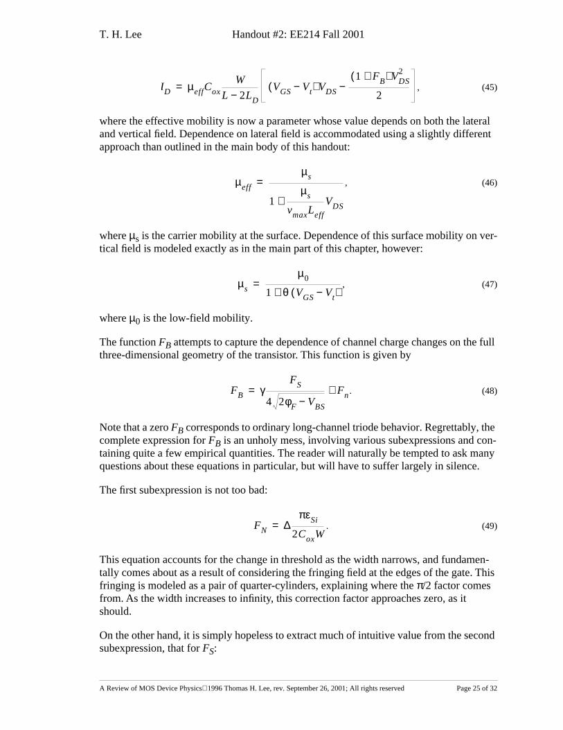
, (45)
where the effective mobility is now a parameter whose value depends on both the lateral and vertical field. Dependence on lateral field is accommodated using a slightly different approach than outlined in the main body of this handout:
, (46)
where
µ
s
is the carrier mobility at the surface. Dependence of this surface mobility on ver-tical field is modeled exactly as in the main part of this chapter, however:
, (47)
where
µ
0
is the low-field mobility.
The function
F
B
attempts to capture the dependence of channel charge changes on the full three-dimensional geometry of the transistor. This function is given by
. (48)
Note that a zero
F
B
corresponds to ordinary long-channel triode behavior. Regrettably, the complete expression for
F
B
is an unholy mess, involving various subexpressions and con-taining quite a few empirical quantities. The reader will naturally be tempted to ask many questions about these equations in particular, but will have to suffer largely in silence.
The first subexpression is not too bad:
. (49)
This equation accounts for the change in threshold as the width narrows, and fundamen-tally comes about as a result of considering the fringing field at the edges of the gate. This fringing is modeled as a pair of quarter-cylinders, explaining where the
π
/2 factor comes from. As the width increases to infinity, this correction factor approaches zero, as it should.
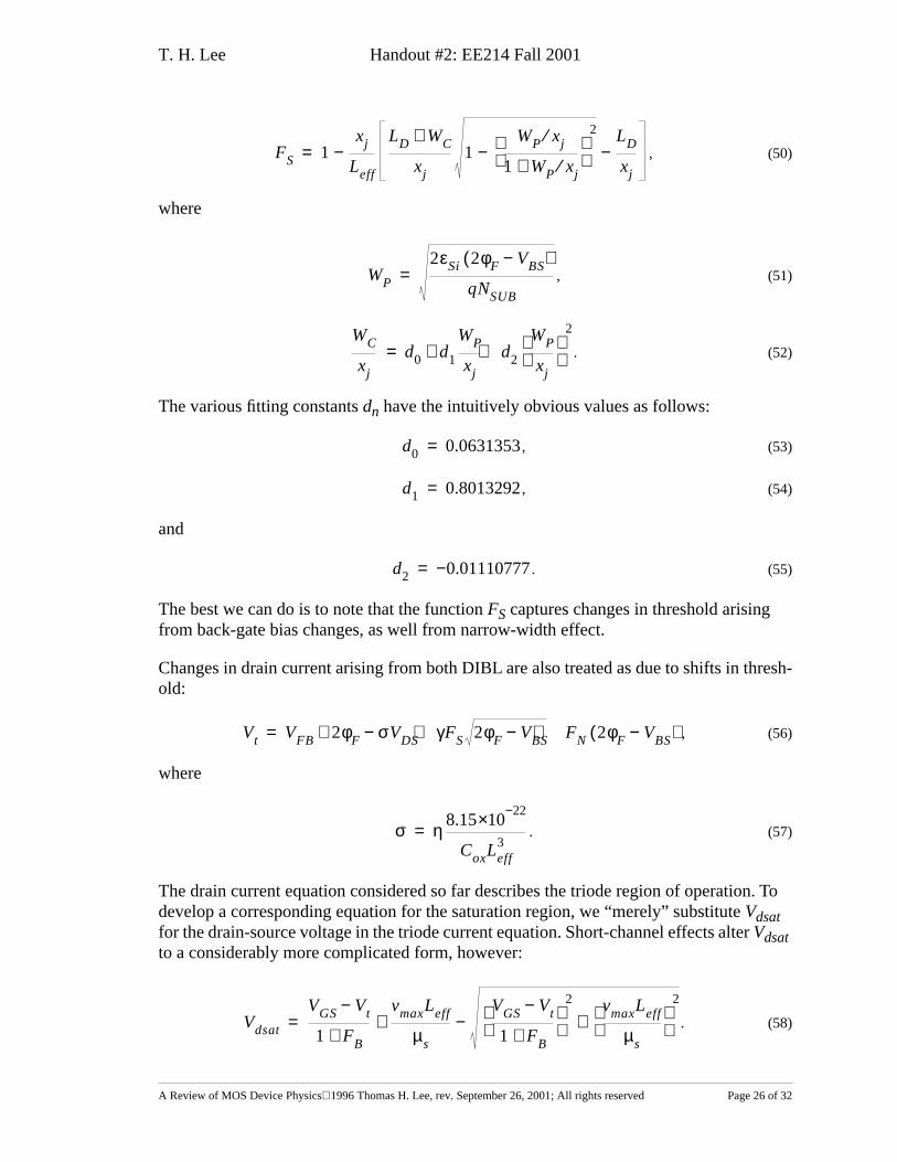
On the other hand, it is simply hopeless to extract much of intuitive value from the second subexpression, that for
F
S
:
ID µeffCoxW
L 2LD−VGS Vt−( ) VDS
1 FB+( ) VDS2
2−=
µeff
µs
1µs
vmaxLeff
VDS+
=
µs
µ0
1 θ VGS Vt−( )+=
FB γFS
4 2φF VBS−Fn+=
FN ∆πεSi
2CoxW=
T. H. Lee Handout #2: EE214 Fall 2001
A Review of MOS Device Physics
1996 Thomas H. Lee, rev. September 26, 2001; All rights reserved Page 26 of 32
, (50)
where
, (51)
. (52)
The various fitting constants
d
n
have the intuitively obvious values as follows:
, (53)
, (54)
and
. (55)
The best we can do is to note that the function
F
S
captures changes in threshold arising from back-gate bias changes, as well from narrow-width effect.
Changes in drain current arising from both DIBL are also treated as due to shifts in thresh-old:
, (56)
where
. (57)
The drain current equation considered so far describes the triode region of operation. To develop a corresponding equation for the saturation region, we “merely” substitute
V
dsat
for the drain-source voltage in the triode current equation. Short-channel effects alter
V
dsat
to a considerably more complicated form, however:
. (58)
FS 1xj
Leff
LD WC+
xj
1WP xj⁄
1 WP xj⁄+
2
−LD
xj
−−=
WP
2εSi 2φF VBS−( )
qNSUB
=
WC
xj
d0 d1
WP
xj
d2
WP
xj
2
+ +=
d0 0.0631353=
d1 0.8013292=
d2 0.01110777−=
Vt VFB 2φF σVDS− γFS 2φF VBS− FN 2φF VBS−( )+ + +=
σ η 8.1522−×10
CoxLeff3
=
Vdsat
VGS Vt−
1 FB+
vmaxLeff
µs
VGS Vt−
1 FB+
2 vmaxLeff
µs
2
+−+=
T. H. Lee Handout #2: EE214 Fall 2001
A Review of MOS Device Physics
1996 Thomas H. Lee, rev. September 26, 2001; All rights reserved Page 27 of 32
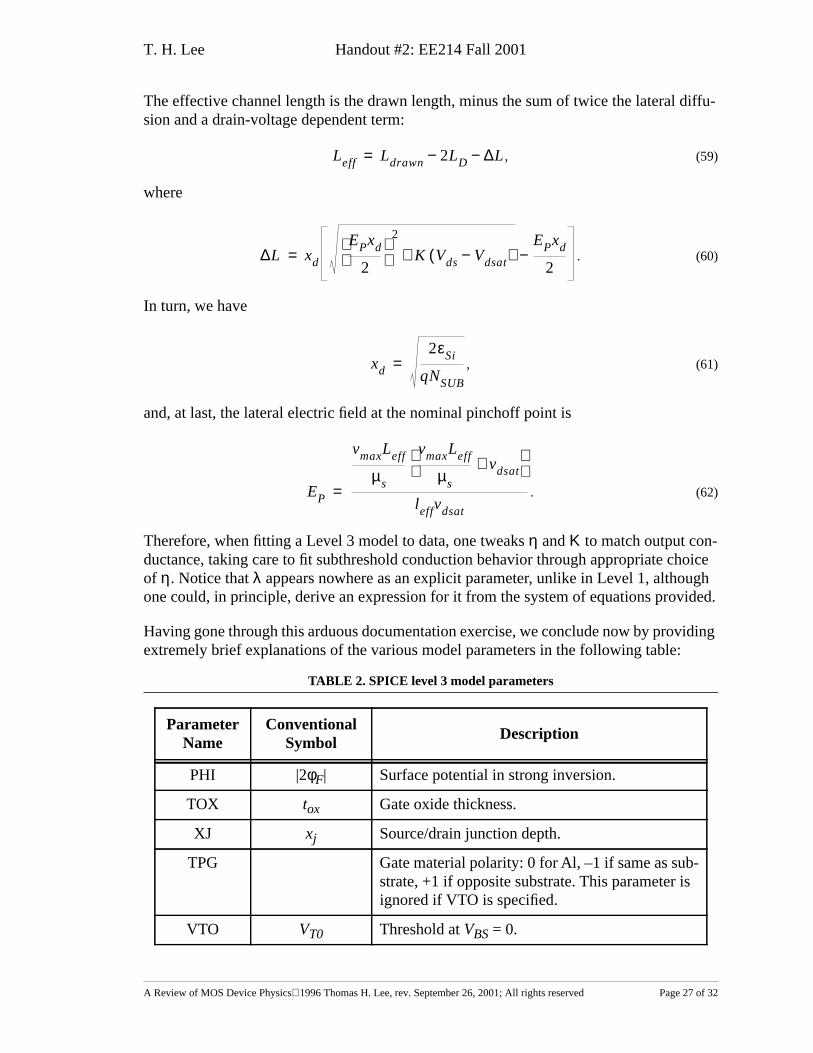
The effective channel length is the drawn length, minus the sum of twice the lateral diffu-sion and a drain-voltage dependent term:
, (59)
where
. (60)
In turn, we have
, (61)
and, at last, the lateral electric field at the nominal pinchoff point is
. (62)
Therefore, when fitting a Level 3 model to data, one tweaks
η
and
Κ
to match output con-ductance, taking care to fit subthreshold conduction behavior through appropriate choice of
η
. Notice that
λ
appears nowhere as an explicit parameter, unlike in Level 1, although one could, in principle, derive an expression for it from the system of equations provided.
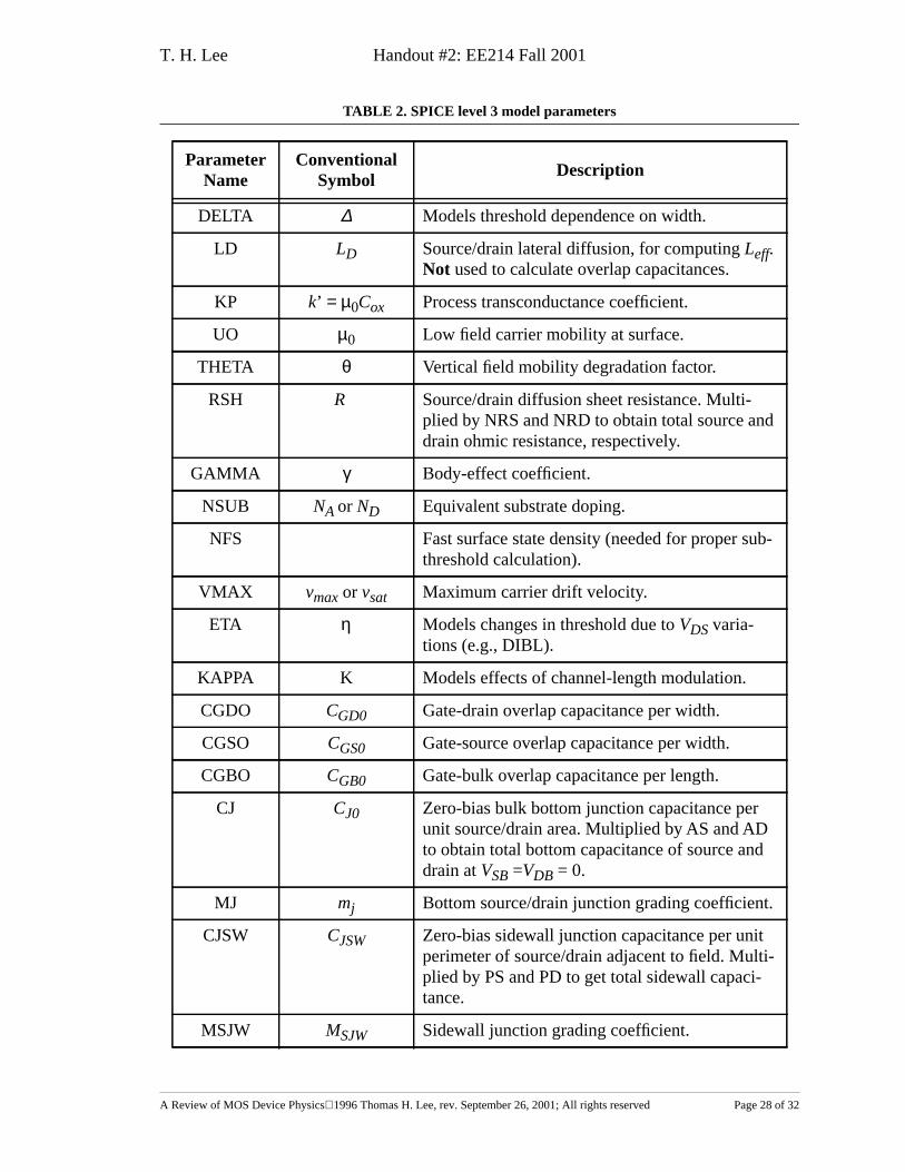
Having gone through this arduous documentation exercise, we conclude now by providing extremely brief explanations of the various model parameters in the following table:
TABLE 2. SPICE level 3 model parameters
Parameter Name
Conventional Symbol
Description
PHI |2
φ
F
| Surface potential in strong inversion.
TOX
t
ox
Gate oxide thickness.
XJ
x
j
Source/drain junction depth.
TPG Gate material polarity: 0 for Al, –1 if same as sub-strate, +1 if opposite substrate. This parameter is ignored if VTO is specified.
VTO
V
T0
Threshold at
V
BS
= 0.
Leff Ldrawn 2LD− ∆L−=
∆L xd
EPxd
2
2
K Vds Vdsat−( )+EPxd
2−=
xd
2εSi
qNSUB
=
EP
vmaxLeff
µs
vmaxLeff
µs
vdsat+
leffvdsat
=
T. H. Lee Handout #2: EE214 Fall 2001
A Review of MOS Device Physics
1996 Thomas H. Lee, rev. September 26, 2001; All rights reserved Page 28 of 32
DELTA
∆
Models threshold dependence on width.
LD
L
D
Source/drain lateral diffusion, for computing
L
eff
.
Not
used to calculate overlap capacitances.
KP
k
’
= µ
0
C
ox
Process transconductance coefficient.
UO
µ
0
Low field carrier mobility at surface.
THETA
θ
Vertical field mobility degradation factor.
RSH
R
Source/drain diffusion sheet resistance. Multi-plied by NRS and NRD to obtain total source and drain ohmic resistance, respectively.
GAMMA
γ
Body-effect coefficient.
NSUB
N
A
or
N
D
Equivalent substrate doping.
NFS Fast surface state density (needed for proper sub-threshold calculation).
VMAX
v
max
or
v
sat
Maximum carrier drift velocity.
ETA
η
Models changes in threshold due to
V
DS
varia-tions (e.g., DIBL).
KAPPA K Models effects of channel-length modulation.
CGDO
C
GD0
Gate-drain overlap capacitance per width.
CGSO
C
GS0
Gate-source overlap capacitance per width.
CGBO
C
GB0
Gate-bulk overlap capacitance per length.
CJ
C
J0
Zero-bias bulk bottom junction capacitance per unit source/drain area. Multiplied by AS and AD to obtain total bottom capacitance of source and drain at
V
SB
=
V
DB
= 0.
MJ
m
j
Bottom source/drain junction grading coefficient.
CJSW
C
JSW
Zero-bias sidewall junction capacitance per unit perimeter of source/drain adjacent to field. Multi-plied by PS and PD to get total sidewall capaci-tance.
MSJW
M
SJW
Sidewall junction grading coefficient.
TABLE 2. SPICE level 3 model parameters
Parameter Name
Conventional Symbol
Description
T. H. Lee Handout #2: EE214 Fall 2001
A Review of MOS Device Physics
1996 Thomas H. Lee, rev. September 26, 2001; All rights reserved Page 29 of 32
As with the Level 1 model, parameters NRS, NRD, AS, AD, PS and PD are all specified in the device description line, not in the model set itself, because they depend on the dimen-sions of the device.
11.1 Deficiencies of the Level 3 model
Although the achievable fits are sometimes remarkably good, it should hardly surprise you that various problems are unavoidable when using something as simple as Level 3 to model something as complex as a modern short-channel MOSFET.
Models of all types often exhibit strange behavior at operating regime boundaries, and Level 3 is unfortunately no exception to this rule. Subthreshold current is improperly cal-culated if parameter NFS is not included. Even when it is included, anomalies in drain cur-rent and transconductance are still to be expected near threshold. Similarly, “strange things” tend to happen to the output conductance near
V
dsat
.
Although narrow-width effects are included in Level 3, the best fits occur if an adjusted width, rather than the drawn width, is used in the device equations. The effective value of width is smaller than the drawn width. In the absence of actual data, a reasonable estimate for the reduction is approximately 10-20% of the minimum drawn channel length. For example, in a 0.18
µ
m process, one should probably subtract about 0.02 -0.04
µ
m from the drawn width, and use the resulting value in all the device equations from that point on.
It is the prevailing wisdom that Level 3 becomes increasingly inaccurate beyond the 1
µ
m technology boundary. The prominence of drain engineering (e.g., use of lightly-doped drains – LDD), among other factors, in modern processes is one of several reasons. At the 0.13
µ
m generation just now making the transition into production from the laboratories, it is quite difficult to obtain good fits with Level 3 models over more than some restricted range of operating voltages, and commercial foundries generally have not bothered with an attempt to develop Level 3 models for several process generations.
12.0 Appendix 2: Level 1 MOS Models
The complexity of MOS device physics is mirrored in the complexity of the models used by commercial simulators. As we’ve emphasized repeatedly,
all
models are “wrong,” and it is up to the circuit designer to use models only where they are sufficiently correct. It is unfortunate that this judgment comes only slowly with experience, but perhaps it is suffi-
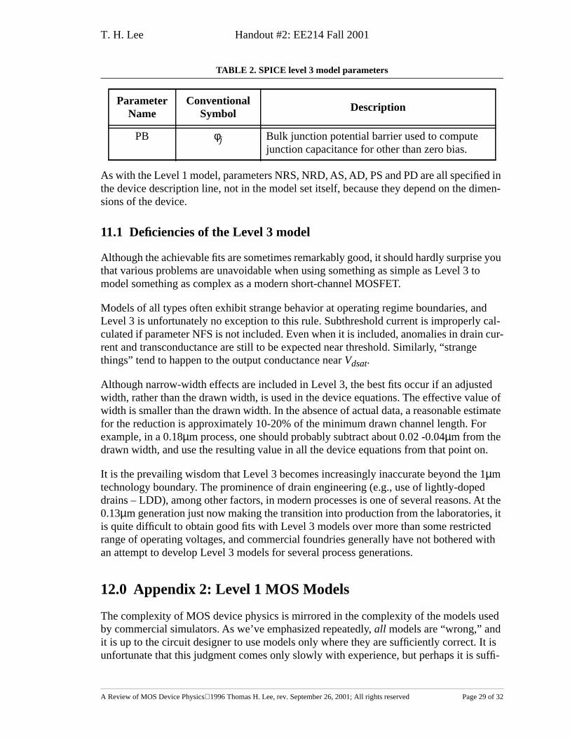
PB
φ
j
Bulk junction potential barrier used to compute junction capacitance for other than zero bias.
TABLE 2. SPICE level 3 model parameters
Parameter Name
Conventional Symbol
Description
T. H. Lee Handout #2: EE214 Fall 2001
A Review of MOS Device Physics
1996 Thomas H. Lee, rev. September 26, 2001; All rights reserved Page 30 of 32
cient here merely to raise awareness of this issue, so that you can be on guard against the possibility (rather, probability) of modeling-induced simulation error.
This brief appendix summarizes the static device equations corresponding to Level 1 SPICE models. By examining these, perhaps you can begin to appreciate the nature of the assumptions underlying their development, and thus also appreciate the origins of their shortcomings.
12.1 The Level 1 static model
The Level 1 SPICE model totally neglects phenomena such as subthreshold conduction, narrow-width effects, lateral-field dependent mobility (including velocity saturation), DIBL, and normal-field mobility degradation. Back-gate bias effect (body effect) is included, but its computation is based on very simple physics. The model can also accom-modate channel-length modulation, but only in a crude way: the user must provide a dif-ferent value of
λ
for each different channel length
. Repeat: Using Level 1, SPICE does not, cannot, and will not automatically recompute
λ
for different channel lengths. This limitation is serious enough that it is advisable to use only devices of channel lengths for which actual experimental data exists, and from which the various values of
λ
are obtained. Level 1 equations for static behavior are thus extremely simple, and correspond most closely to those outlined in the main development of both the textbook and the main body of this handout.
Recall that, in triode, the drain current of an NMOS transistor with drawn dimensions
W
/
L
is given by:
, (63)
while the saturation drain current is given by:
. (64)
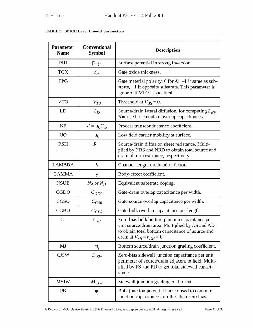
The model comprises the parameters in the following table, which also provides mathe-matical translations where necessary:
ID µnCoxW
L 2LD−VGS Vt−( ) VDS
VDS2
2− 1 λVDS+( )=
ID µnCoxW
2 L 2LD−( )VGS Vt−( ) 2 1 λVDS+( )=
T. H. Lee Handout #2: EE214 Fall 2001
A Review of MOS Device Physics
1996 Thomas H. Lee, rev. September 26, 2001; All rights reserved Page 31 of 32
TABLE 3. SPICE Level 1 model parameters
Parameter Name
Conventional Symbol
Description
PHI |2
φ
F
| Surface potential in strong inversion.
TOX
t
ox
Gate oxide thickness.
TPG Gate material polarity: 0 for Al, –1 if same as sub-strate, +1 if opposite substrate. This parameter is ignored if VTO is specified.
VTO
V
T0
Threshold at
V
BS
= 0.
LD
L
D
Source/drain lateral diffusion, for computing
L
eff
.
Not
used to calculate overlap capacitances.
KP
k
’
= µ
0
C
ox
Process transconductance coefficient.
UO
µ
0
Low field carrier mobility at surface.
RSH
R
Source/drain diffusion sheet resistance. Multi-plied by NRS and NRD to obtain total source and drain ohmic resistance, respectively.
LAMBDA
λ
Channel-length modulation factor.
GAMMA
γ
Body-effect coefficient.
NSUB
N
A
or
N
D
Equivalent substrate doping.
CGDO
C
GD0
Gate-drain overlap capacitance per width.
CGSO
C
GS0
Gate-source overlap capacitance per width.
CGBO
C
GB0
Gate-bulk overlap capacitance per length.
CJ
C
J0
Zero-bias bulk bottom junction capacitance per unit source/drain area. Multiplied by AS and AD to obtain total bottom capacitance of source and drain at
V
SB
=
V
DB
= 0.
MJ
m
j
Bottom source/drain junction grading coefficient.
CJSW
C
JSW
Zero-bias sidewall junction capacitance per unit perimeter of source/drain adjacent to field. Multi-plied by PS and PD to get total sidewall capaci-tance.
MSJW
M
SJW
Sidewall junction grading coefficient.
PB
φ
j
Bulk junction potential barrier used to compute junction capacitance for other than zero bias.
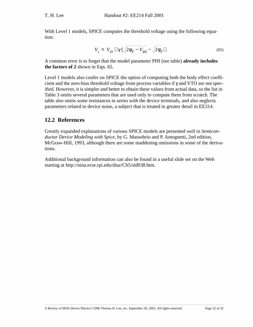
T. H. Lee Handout #2: EE214 Fall 2001
A Review of MOS Device Physics
1996 Thomas H. Lee, rev. September 26, 2001; All rights reserved Page 32 of 32
With Level 1 models, SPICE computes the threshold voltage using the following equa-tion:
. (65)
A common error is to forget that the model parameter PHI (see table)
already includes the factors of 2
shown in Eqn. 65.
Level 1 models also confer on SPICE the option of computing both the body effect coeffi-cient and the zero-bias threshold voltage from process variables if
γ
and VTO are not spec-ified. However, it is simpler and better to obtain these values from actual data, so the list in Table 3 omits several parameters that are used only to compute them from scratch. The table also omits some resistances in series with the device terminals, and also neglects parameters related to device noise, a subject that is treated in greater detail in EE314.
12.2 References
Greatly expanded explanations of various SPICE models are presented well in
Semicon-ductor Device Modeling with Spice
, by G. Massobrio and P. Antognetti, 2nd edition, McGraw-Hill, 1993, although there are some maddening omissions in some of the deriva-tions.
Additional background information can also be found in a useful slide set on the Web starting at http://nina.ecse.rpi.edu/shur/Ch5/sld038.htm.
Vt Vt0 γ 2φF VBS− 2φF−( )+=