High Voltage DC/DC Boost Converter w/0.5A/1.3A …€¢10-Pin3 mm×3 mm QFN Package USB output. The...
23
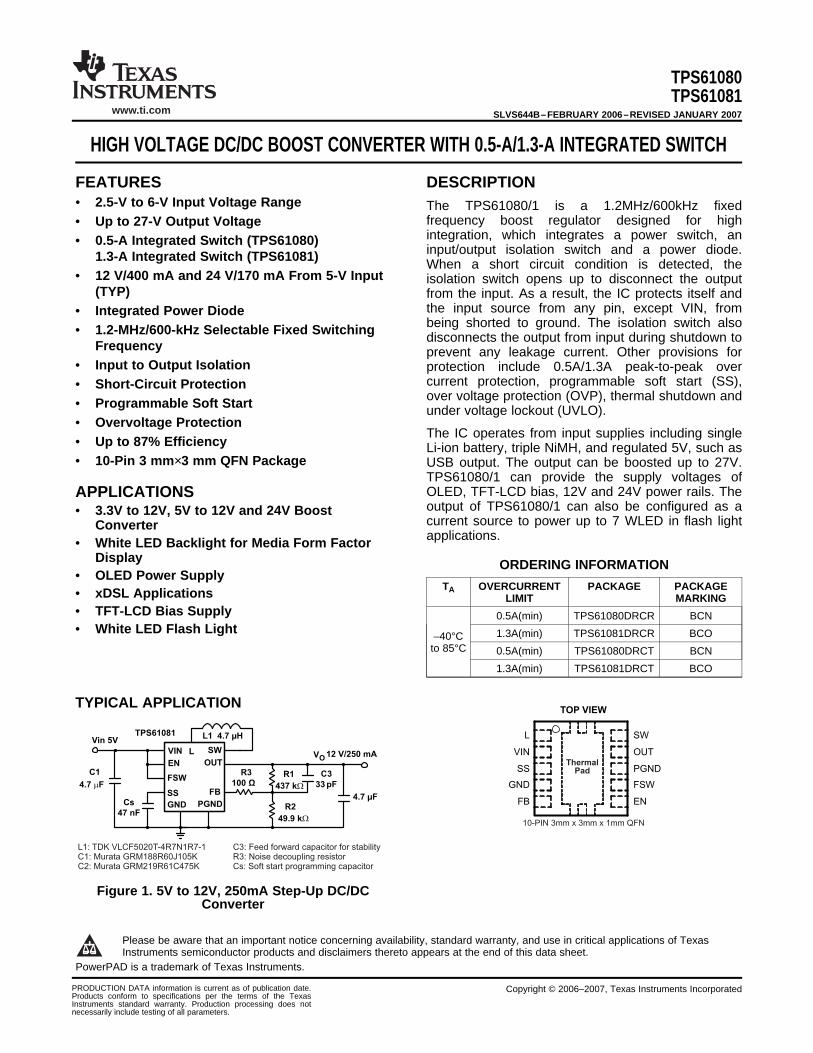
www.ti.com FEATURES DESCRIPTION APPLICATIONS TYPICAL APPLICATION FSW SW OUT PGND EN GND L VIN SS FB TOP VIEW 10-PIN 3mm x 3mm x 1mm QFN Thermal Pad Vin 5V L1 4.7 μH C1 4.7 F m C3 33 pF V O 12 V/250 mA R1 437 kW Cs 47 nF R3 100 Ω R2 49.9 kW 4.7 μF TPS61081 L1: TDK VLCF5020T-4R7N1R7-1 C3: Feed forward capacitor for stability C1: Murata GRM188R60J105K R3: Noise decoupling resistor C2: Murata GRM219R61C475K Cs: Soft start programming capacitor L VIN EN FSW SS GND SW OUT FB PGND TPS61080 TPS61081 SLVS644B – FEBRUARY 2006 – REVISED JANUARY 2007 HIGH VOLTAGE DC/DC BOOST CONVERTER WITH 0.5-A/1.3-A INTEGRATED SWITCH • 2.5-V to 6-V Input Voltage Range The TPS61080/1 is a 1.2MHz/600kHz fixed frequency boost regulator designed for high • Up to 27-V Output Voltage integration, which integrates a power switch, an • 0.5-A Integrated Switch (TPS61080) input/output isolation switch and a power diode. 1.3-A Integrated Switch (TPS61081) When a short circuit condition is detected, the • 12 V/400 mA and 24 V/170 mA From 5-V Input isolation switch opens up to disconnect the output (TYP) from the input. As a result, the IC protects itself and the input source from any pin, except VIN, from • Integrated Power Diode being shorted to ground. The isolation switch also • 1.2-MHz/600-kHz Selectable Fixed Switching disconnects the output from input during shutdown to Frequency prevent any leakage current. Other provisions for • Input to Output Isolation protection include 0.5A/1.3A peak-to-peak over current protection, programmable soft start (SS), • Short-Circuit Protection over voltage protection (OVP), thermal shutdown and • Programmable Soft Start under voltage lockout (UVLO). • Overvoltage Protection The IC operates from input supplies including single • Up to 87% Efficiency Li-ion battery, triple NiMH, and regulated 5V, such as • 10-Pin 3 mm×3 mm QFN Package USB output. The output can be boosted up to 27V. TPS61080/1 can provide the supply voltages of OLED, TFT-LCD bias, 12V and 24V power rails. The output of TPS61080/1 can also be configured as a • 3.3V to 12V, 5V to 12V and 24V Boost current source to power up to 7 WLED in flash light Converter applications. • White LED Backlight for Media Form Factor Display ORDERING INFORMATION • OLED Power Supply T A OVERCURRENT PACKAGE PACKAGE • xDSL Applications LIMIT MARKING • TFT-LCD Bias Supply 0.5A(min) TPS61080DRCR BCN • White LED Flash Light 1.3A(min) TPS61081DRCR BCO –40°C to 85°C 0.5A(min) TPS61080DRCT BCN 1.3A(min) TPS61081DRCT BCO Figure 1. 5V to 12V, 250mA Step-Up DC/DC Converter Please be aware that an important notice concerning availability, standard warranty, and use in critical applications of Texas Instruments semiconductor products and disclaimers thereto appears at the end of this data sheet. PowerPAD is a trademark of Texas Instruments. PRODUCTION DATA information is current as of publication date. Copyright © 2006–2007, Texas Instruments Incorporated Products conform to specifications per the terms of the Texas Instruments standard warranty. Production processing does not necessarily include testing of all parameters.
Transcript of High Voltage DC/DC Boost Converter w/0.5A/1.3A …€¢10-Pin3 mm×3 mm QFN Package USB output. The...
www.ti.com
FEATURES DESCRIPTION
APPLICATIONS
TYPICAL APPLICATION
FSW
SW
OUT
PGND
EN
GND
L
VIN
SS
FB
TOP VIEW
10-PIN 3mm x 3mm x 1mm QFN
Thermal
Pad
Vin 5VL1 4.7 µH
C1
4.7 Fm
C3
33 pF
VO12 V/250 mA
R1
437 kW
Cs
47 nF
R3
100 Ω
R2
49.9 kW
4.7 µF
TPS61081
L1: TDK VLCF5020T-4R7N1R7-1 C3: Feed forward capacitor for stabilityC1: Murata GRM188R60J105K R3: Noise decoupling resistorC2: Murata GRM219R61C475K Cs: Soft start programming capacitor
LVIN
EN
FSW
SS
GND
SW
OUT
FB
PGND
TPS61080TPS61081
SLVS644B–FEBRUARY 2006–REVISED JANUARY 2007
HIGH VOLTAGE DC/DC BOOST CONVERTER WITH 0.5-A/1.3-A INTEGRATED SWITCH
• 2.5-V to 6-V Input Voltage Range The TPS61080/1 is a 1.2MHz/600kHz fixedfrequency boost regulator designed for high• Up to 27-V Output Voltageintegration, which integrates a power switch, an• 0.5-A Integrated Switch (TPS61080)input/output isolation switch and a power diode.1.3-A Integrated Switch (TPS61081)When a short circuit condition is detected, the
• 12 V/400 mA and 24 V/170 mA From 5-V Input isolation switch opens up to disconnect the output(TYP) from the input. As a result, the IC protects itself and
the input source from any pin, except VIN, from• Integrated Power Diodebeing shorted to ground. The isolation switch also• 1.2-MHz/600-kHz Selectable Fixed Switching disconnects the output from input during shutdown to
Frequency prevent any leakage current. Other provisions for• Input to Output Isolation protection include 0.5A/1.3A peak-to-peak over
current protection, programmable soft start (SS),• Short-Circuit Protectionover voltage protection (OVP), thermal shutdown and• Programmable Soft Start under voltage lockout (UVLO).
• Overvoltage ProtectionThe IC operates from input supplies including single• Up to 87% Efficiency Li-ion battery, triple NiMH, and regulated 5V, such as
• 10-Pin 3 mm×3 mm QFN Package USB output. The output can be boosted up to 27V.TPS61080/1 can provide the supply voltages ofOLED, TFT-LCD bias, 12V and 24V power rails. Theoutput of TPS61080/1 can also be configured as a• 3.3V to 12V, 5V to 12V and 24V Boostcurrent source to power up to 7 WLED in flash lightConverterapplications.• White LED Backlight for Media Form Factor
Display ORDERING INFORMATION• OLED Power Supply
TA OVERCURRENT PACKAGE PACKAGE• xDSL Applications LIMIT MARKING• TFT-LCD Bias Supply 0.5A(min) TPS61080DRCR BCN• White LED Flash Light 1.3A(min) TPS61081DRCR BCO–40°C
to 85°C 0.5A(min) TPS61080DRCT BCN
1.3A(min) TPS61081DRCT BCO
Figure 1. 5V to 12V, 250mA Step-Up DC/DCConverter
Please be aware that an important notice concerning availability, standard warranty, and use in critical applications of TexasInstruments semiconductor products and disclaimers thereto appears at the end of this data sheet.
PowerPAD is a trademark of Texas Instruments.
PRODUCTION DATA information is current as of publication date. Copyright © 2006–2007, Texas Instruments IncorporatedProducts conform to specifications per the terms of the TexasInstruments standard warranty. Production processing does notnecessarily include testing of all parameters.
www.ti.com
L1 10
SW
Charge
Pump
2
VIN
EN SC
RampGenerator
Oscillator
FB5
Clamp
MUX
BandGap
1.229VSS
EN
PWMControl
Current
Sensor
Error
Amplifer
OVP
ThermalShutdown
OVP
ShortCircuit9
OUT
FSW7
PGND8
SC OVP
1.2MHz
600KHz
6
3
GND4
+
FB
R1
R2 R3
C3
C2
Cs
C1
L1
TPS61080TPS61081SLVS644B–FEBRUARY 2006–REVISED JANUARY 2007
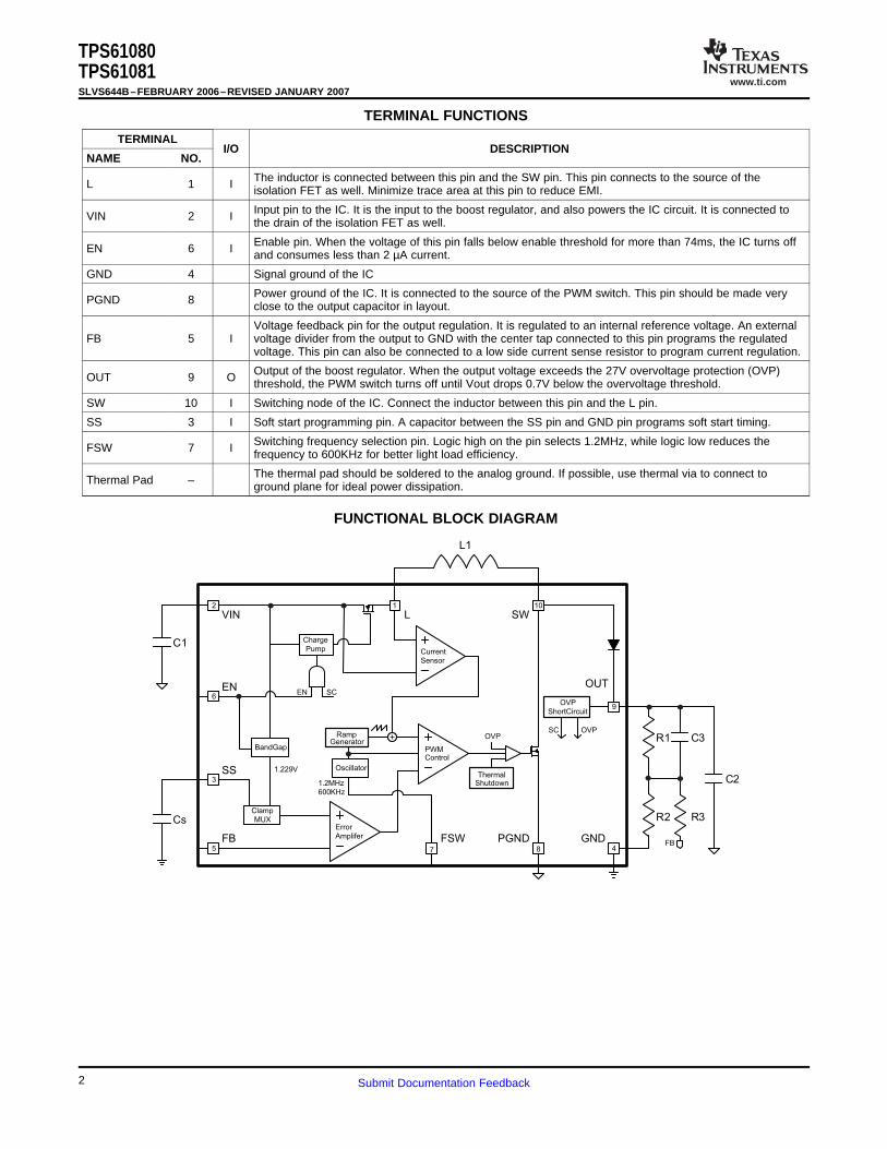
TERMINAL FUNCTIONS
TERMINALI/O DESCRIPTION
NAME NO.
The inductor is connected between this pin and the SW pin. This pin connects to the source of theL 1 I isolation FET as well. Minimize trace area at this pin to reduce EMI.
Input pin to the IC. It is the input to the boost regulator, and also powers the IC circuit. It is connected toVIN 2 I the drain of the isolation FET as well.
Enable pin. When the voltage of this pin falls below enable threshold for more than 74ms, the IC turns offEN 6 I and consumes less than 2 µA current.
GND 4 Signal ground of the IC
Power ground of the IC. It is connected to the source of the PWM switch. This pin should be made veryPGND 8 close to the output capacitor in layout.
Voltage feedback pin for the output regulation. It is regulated to an internal reference voltage. An externalFB 5 I voltage divider from the output to GND with the center tap connected to this pin programs the regulated
voltage. This pin can also be connected to a low side current sense resistor to program current regulation.
Output of the boost regulator. When the output voltage exceeds the 27V overvoltage protection (OVP)OUT 9 O threshold, the PWM switch turns off until Vout drops 0.7V below the overvoltage threshold.
SW 10 I Switching node of the IC. Connect the inductor between this pin and the L pin.
SS 3 I Soft start programming pin. A capacitor between the SS pin and GND pin programs soft start timing.
Switching frequency selection pin. Logic high on the pin selects 1.2MHz, while logic low reduces theFSW 7 I frequency to 600KHz for better light load efficiency.
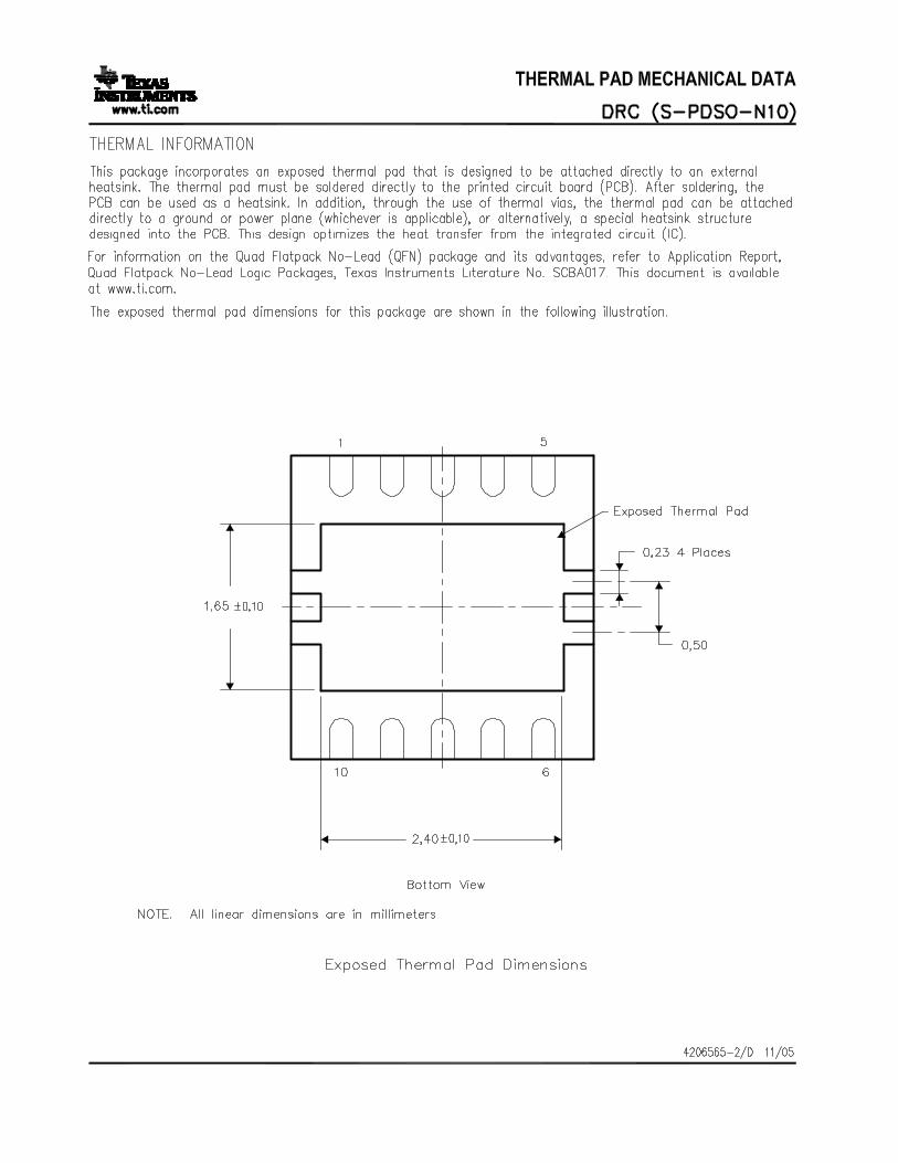
The thermal pad should be soldered to the analog ground. If possible, use thermal via to connect toThermal Pad – ground plane for ideal power dissipation.
FUNCTIONAL BLOCK DIAGRAM
2 Submit Documentation Feedback
www.ti.com
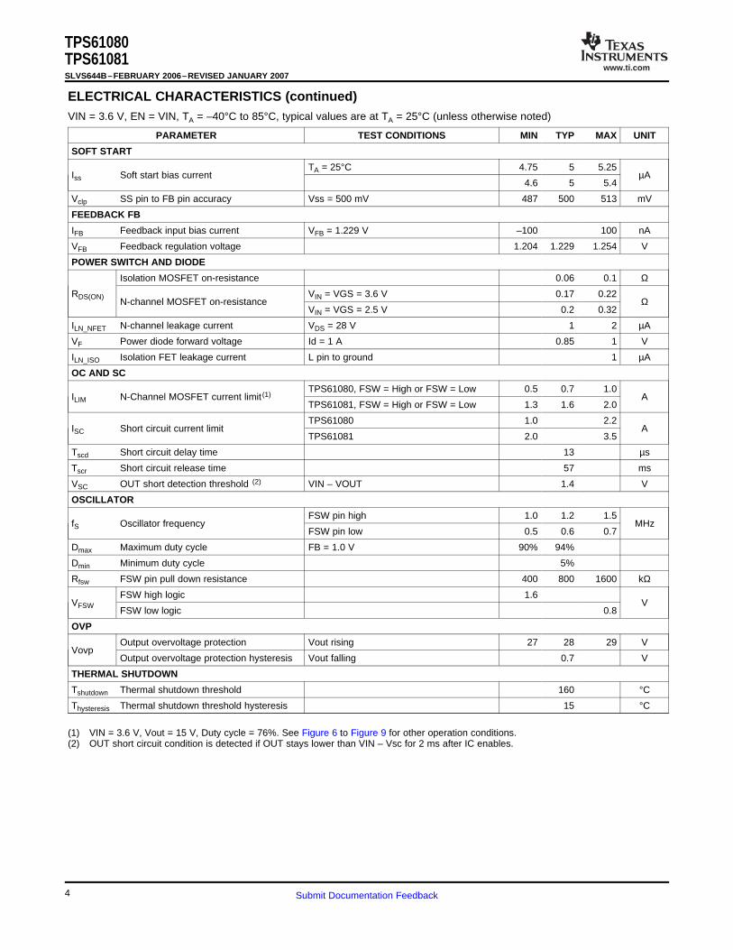
ABSOLUTE MAXIMUM RATINGS
DISSIPATION RATINGS
RECOMMENDED OPERATING CONDITIONS
ELECTRICAL CHARACTERISTICS
TPS61080TPS61081
SLVS644B–FEBRUARY 2006–REVISED JANUARY 2007
over operating free-air temperature range (unless otherwise noted) (1)
VALUE UNIT
Supply Voltages on pin VIN (2) –0.3 to 7 V
Voltages on pins EN, FB, SS, L and FSW (2) –0.3 to 7 V
Voltage on pin OUT (2) 30V V
Voltage on pin SW (2) 30V V
Continuous Power Dissipation See Dissipation Rating Table
Operating Junction Temperature Range –40 to 150 °C
Storage Temperature Range –65 to 150 °C
Lead Temperature (soldering, 10 sec) 260 °C
(1) Stresses beyond those listed under absolute maximum ratings may cause permanent damage to the device. These are stress ratingsonly, and functional operation of the device at these or any other conditions beyond those indicated under recommended operatingconditions is not implied. Exposure to absolute-maximum-rated conditions for extended periods may affect device reliability.
(2) All voltage values are with respect to network ground terminal.
TA≤ 25°C TA = 70°C TA = 85°CPACKAGE θJC θJA POWER RATING POWER RATING POWER RATING
QFN (1) 3.21°C/W 270°C/W 370 mW 204 mW 148 mW
QFN (2) 3.21°C/W 48.7°C/W 2.05 W 1.13 W 821 mW
(1) Soldered PowerPAD™ on a standard 2-layer PCB without vias for thermal pad(2) Soldered PowerPAD on a standard 4-layer PCB with vias for thermal pad
over operating free-air temperature range (unless otherwise noted)
MIN NOM MAX UNIT
VIN Input voltage range 2.5 6.0 V
VOUT Output voltage range VIN 27 V
L Inductor (1) 4.7 10 µH
Cin Input capacitor (1) 1 µF
COUT Output capacitor (1) 4.7 µF
TA Operating ambient temperature –40 85 °C
TJ Operating junction temperature –40 125 °C
(1) Refer to application section for further information
VIN = 3.6 V, EN = VIN, TA = –40°C to 85°C, typical values are at TA = 25°C (unless otherwise noted)
PARAMETER TEST CONDITIONS MIN TYP MAX UNIT
SUPPLY CURRENT
VIN Input voltage range 2.5 6.0 V
IQ Operating quiescent current into VIN Device switching no load 6 mA
ISD Shutdown current EN = GND 1 µA
VUVLO Under-voltage lockout threshold VIN falling 1.65 1.8 V
Vhys Under-voltage lockout hysterisis 50 mV
ENABLE
Enable level voltage VIN = 2.5 V to 6 V 1.2VEN V
Disable level voltage VIN = 2.5 V to 6 V 0.4
Ren Enable pull down resistor 400 800 1600 kΩ
Toff EN pulse width to disable EN high to low 74 ms
3Submit Documentation Feedback
www.ti.com
TPS61080TPS61081SLVS644B–FEBRUARY 2006–REVISED JANUARY 2007
ELECTRICAL CHARACTERISTICS (continued)VIN = 3.6 V, EN = VIN, TA = –40°C to 85°C, typical values are at TA = 25°C (unless otherwise noted)
PARAMETER TEST CONDITIONS MIN TYP MAX UNIT
SOFT START
TA = 25°C 4.75 5 5.25Iss Soft start bias current µA
4.6 5 5.4
Vclp SS pin to FB pin accuracy Vss = 500 mV 487 500 513 mV
FEEDBACK FB
IFB Feedback input bias current VFB = 1.229 V –100 100 nA
VFB Feedback regulation voltage 1.204 1.229 1.254 V
POWER SWITCH AND DIODE
Isolation MOSFET on-resistance 0.06 0.1 Ω
RDS(ON) VIN = VGS = 3.6 V 0.17 0.22N-channel MOSFET on-resistance Ω
VIN = VGS = 2.5 V 0.2 0.32
ILN_NFET N-channel leakage current VDS = 28 V 1 2 µA
VF Power diode forward voltage Id = 1 A 0.85 1 V
ILN_ISO Isolation FET leakage current L pin to ground 1 µA
OC AND SC
TPS61080, FSW = High or FSW = Low 0.5 0.7 1.0ILIM N-Channel MOSFET current limit (1) A
TPS61081, FSW = High or FSW = Low 1.3 1.6 2.0
TPS61080 1.0 2.2ISC Short circuit current limit A
TPS61081 2.0 3.5
Tscd Short circuit delay time 13 µs
Tscr Short circuit release time 57 ms
VSC OUT short detection threshold (2) VIN – VOUT 1.4 V
OSCILLATOR
FSW pin high 1.0 1.2 1.5fS Oscillator frequency MHz
FSW pin low 0.5 0.6 0.7
Dmax Maximum duty cycle FB = 1.0 V 90% 94%
Dmin Minimum duty cycle 5%
Rfsw FSW pin pull down resistance 400 800 1600 kΩ
FSW high logic 1.6VFSW V
FSW low logic 0.8
OVP
Output overvoltage protection Vout rising 27 28 29 VVovp
Output overvoltage protection hysteresis Vout falling 0.7 V
THERMAL SHUTDOWN
Tshutdown Thermal shutdown threshold 160 °C
Thysteresis Thermal shutdown threshold hysteresis 15 °C
(1) VIN = 3.6 V, Vout = 15 V, Duty cycle = 76%. See Figure 6 to Figure 9 for other operation conditions.(2) OUT short circuit condition is detected if OUT stays lower than VIN – Vsc for 2 ms after IC enables.
4 Submit Documentation Feedback
www.ti.com
TYPICAL CHARACTERISTICS
40
50
60
70
80
90
100
0 50 100 150 200 250 300
I - Output Current - mAO
Eff
icie
nc
y -
%
V = 12 VOV = 20 VO
V = 16 VO
V = 25 VO
V = 3.6 VI
40
50
60
70
80
90
100
0 50 100 150 200 250 300
I - Output Current - mAO
Eff
icie
nc
y -
%
V = 3.6 VI
V = 25 VO V = 20 VO
V = 16 VOV = 12 VO
TPS61080TPS61081
SLVS644B–FEBRUARY 2006–REVISED JANUARY 2007
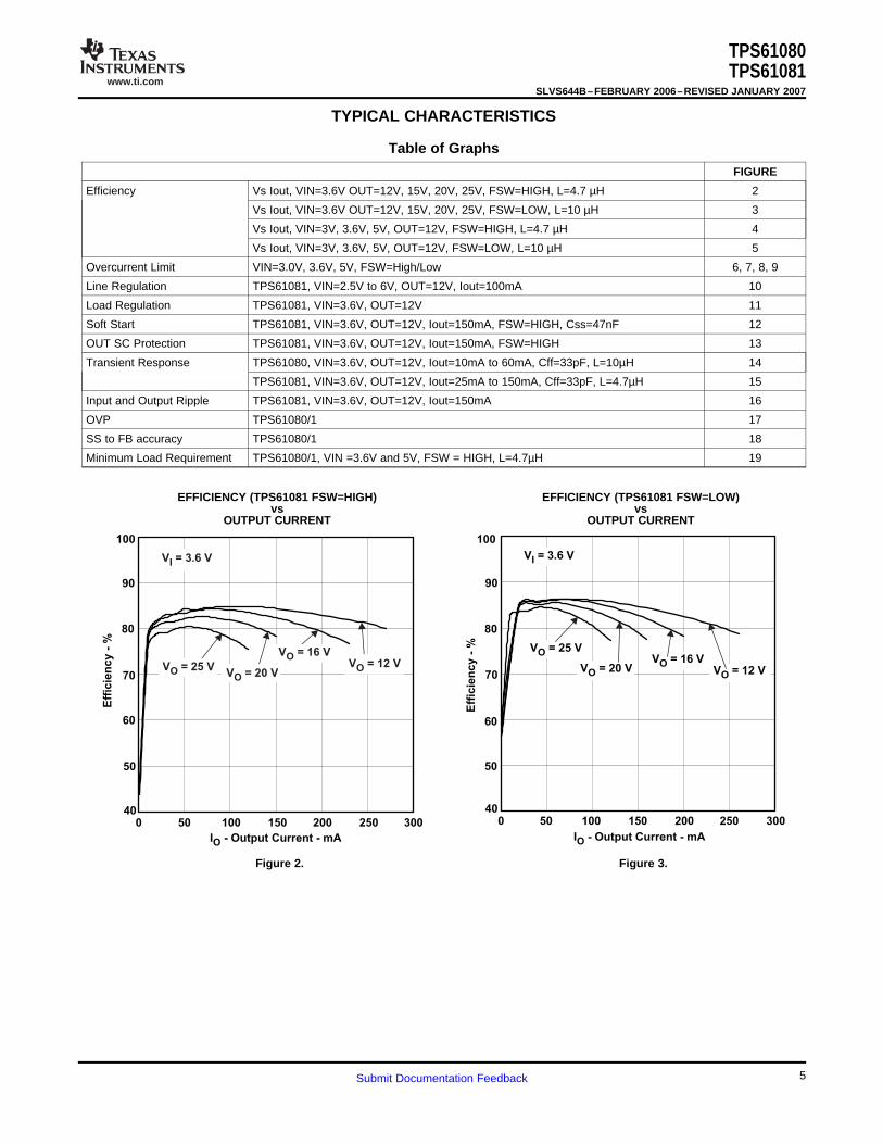
Table of Graphs
FIGURE
Efficiency Vs Iout, VIN=3.6V OUT=12V, 15V, 20V, 25V, FSW=HIGH, L=4.7 µH 2
Vs Iout, VIN=3.6V OUT=12V, 15V, 20V, 25V, FSW=LOW, L=10 µH 3
Vs Iout, VIN=3V, 3.6V, 5V, OUT=12V, FSW=HIGH, L=4.7 µH 4
Vs Iout, VIN=3V, 3.6V, 5V, OUT=12V, FSW=LOW, L=10 µH 5
Overcurrent Limit VIN=3.0V, 3.6V, 5V, FSW=High/Low 6, 7, 8, 9
Line Regulation TPS61081, VIN=2.5V to 6V, OUT=12V, Iout=100mA 10
Load Regulation TPS61081, VIN=3.6V, OUT=12V 11
Soft Start TPS61081, VIN=3.6V, OUT=12V, Iout=150mA, FSW=HIGH, Css=47nF 12
OUT SC Protection TPS61081, VIN=3.6V, OUT=12V, Iout=150mA, FSW=HIGH 13
Transient Response TPS61080, VIN=3.6V, OUT=12V, Iout=10mA to 60mA, Cff=33pF, L=10µH 14
TPS61081, VIN=3.6V, OUT=12V, Iout=25mA to 150mA, Cff=33pF, L=4.7µH 15
Input and Output Ripple TPS61081, VIN=3.6V, OUT=12V, Iout=150mA 16
OVP TPS61080/1 17
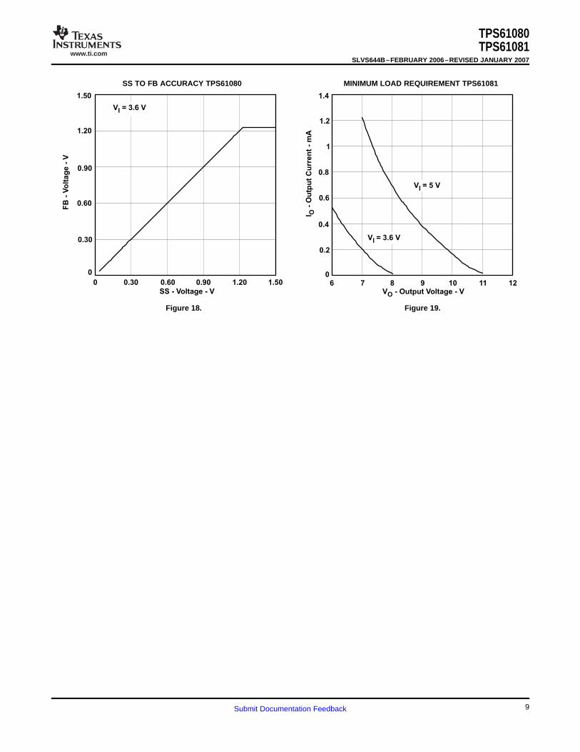
SS to FB accuracy TPS61080/1 18
Minimum Load Requirement TPS61080/1, VIN =3.6V and 5V, FSW = HIGH, L=4.7µH 19
EFFICIENCY (TPS61081 FSW=HIGH) EFFICIENCY (TPS61081 FSW=LOW)vs vs
OUTPUT CURRENT OUTPUT CURRENT
Figure 2. Figure 3.
5Submit Documentation Feedback
www.ti.com
30
40
50
60
70
80
90
100
0 50 100 150 200 250 300 350
I - Output Current - mAO
Eff
icie
nc
y -
% V = 5 VIV = 3 VI V = 3.6 VI
V = 12 VO
30
40
50
60
70
80
90
100
0 50 100 150 200 250 300 350
I - Output Current - mAOE
ffic
ien
cy
- %
V = 5 VIV = 3 VI
V = 3.6 VI
V = 12 VO
0
0.2
0.4
0.6
0.8
1
20 30 40 50 60 70 80 90
Duty Cycle - %
Cu
rre
nt
Lim
it -
A V = 3 VI V = 5 VI
V = 3.6 VI
0
0.2
0.4
0.6
0.8
1
20 30 40 50 60 70 80 90
Duty Cycle - %
Cu
rre
nt
Lim
it -
A
V = 3 VIV = 5 VI
V = 3.6 VI
TPS61080TPS61081SLVS644B–FEBRUARY 2006–REVISED JANUARY 2007
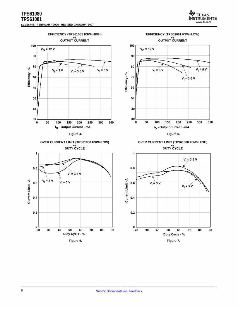
EFFICIENCY (TPS61081 FSW=HIGH) EFFICIENCY (TPS61081 FSW=LOW)vs vs
OUTPUT CURRENT OUTPUT CURRENT
Figure 4. Figure 5.
OVER CURRENT LIMIT (TPS61080 FSW=LOW) OVER CURRENT LIMIT (TPS61080 FSW=HIGH)vs vs
DUTY CYCLE DUTY CYCLE
Figure 6. Figure 7.
6 Submit Documentation Feedback
www.ti.com
0
0.40
0.80
1.20
1.60
2
20 30 40 50 60 70 80 90Duty Cycle - %
Cu
rre
nt
Lim
it -
A
V = 3 VI
V = 5 VI
V = 3.6 VI
0
0.40
0.80
1.20
1.60
2
20 30 40 50 60 70 80 90
Duty Cycle - %
Cu
rre
nt
Lim
it -
A
V = 3 VI
V = 5 VI V = 3.6 VI
I = 150 mAO
I = 100 mAO
2.5 3 3.5 4 4.5 5 5.5 6
V - Input Voltage - VI
12.21
12.22
12.23
12.24
12.25
12.26
12.27
12.28
12.29
12.30
V-
Ou
tpu
t V
olt
ag
e -
VO
T = -40 °CA
T = 25 °CA
T = 85 °CA
12.20
12.22
12.24
12.26
12.28
12.30
12.32
0 0.05 0.10 0.15 0.20 0.25 0.30
I - Output Current - AO
V-
Ou
tpu
t V
olt
ag
e -
VO
T = 85 °CA
T = 25 °CA
T = -40 °CA
V = 3.6 VI
V = 5 VI
TPS61080TPS61081
SLVS644B–FEBRUARY 2006–REVISED JANUARY 2007
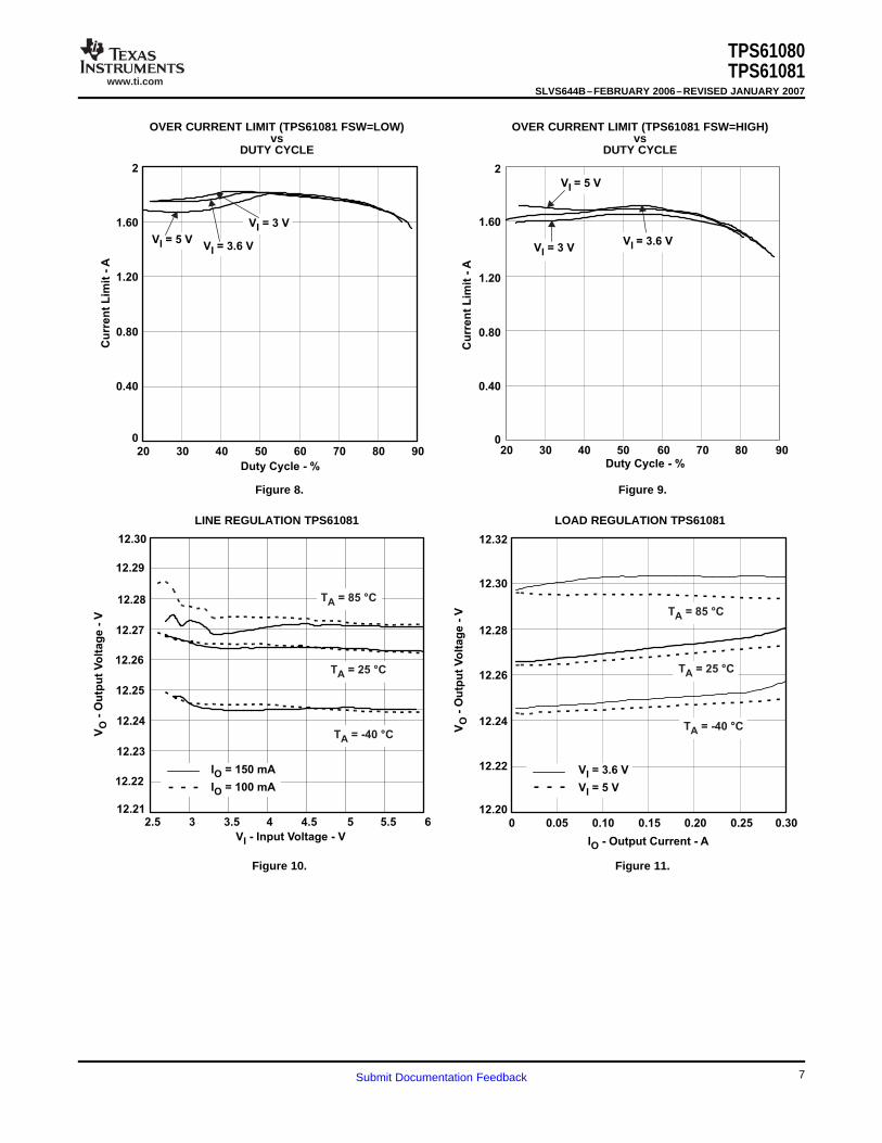
OVER CURRENT LIMIT (TPS61081 FSW=LOW) OVER CURRENT LIMIT (TPS61081 FSW=HIGH)vs vs
DUTY CYCLE DUTY CYCLE
Figure 8. Figure 9.
LINE REGULATION TPS61081 LOAD REGULATION TPS61081
Figure 10. Figure 11.
7Submit Documentation Feedback
www.ti.com
Input Current
500mA/div, DC
OUT
10V/div, DC
SS
2V/div, DC
Inductor Current
500mA/div, DC
t - Time - 4 ms/div
Input Current
2A/div, DC
SW
10V/div, DC
OUT
10V/div, DC
L
5V/div, DC
t - Time - 10 s/divm
OUT
100 mV/div, AC
Output Current
50 mA/div, DC
t - Time - 400 s/divm
OUT
200 mV/div, AC
Output Current
100 mA/div, DC
t - Time - 400 s/divm
OUT
1 V/div, DC
27 V Offset
SW
20 V/div, DC
Inductor Current
1 A/div, DC
t - Time - 20 ns/div
OUT
50 mV/div, AC
VIN
50 mV/div, AC
SW
10 V/div, DC
Inductor Current
500 mA/div, DC
t - Time - 400 ns/div
TPS61080TPS61081SLVS644B–FEBRUARY 2006–REVISED JANUARY 2007
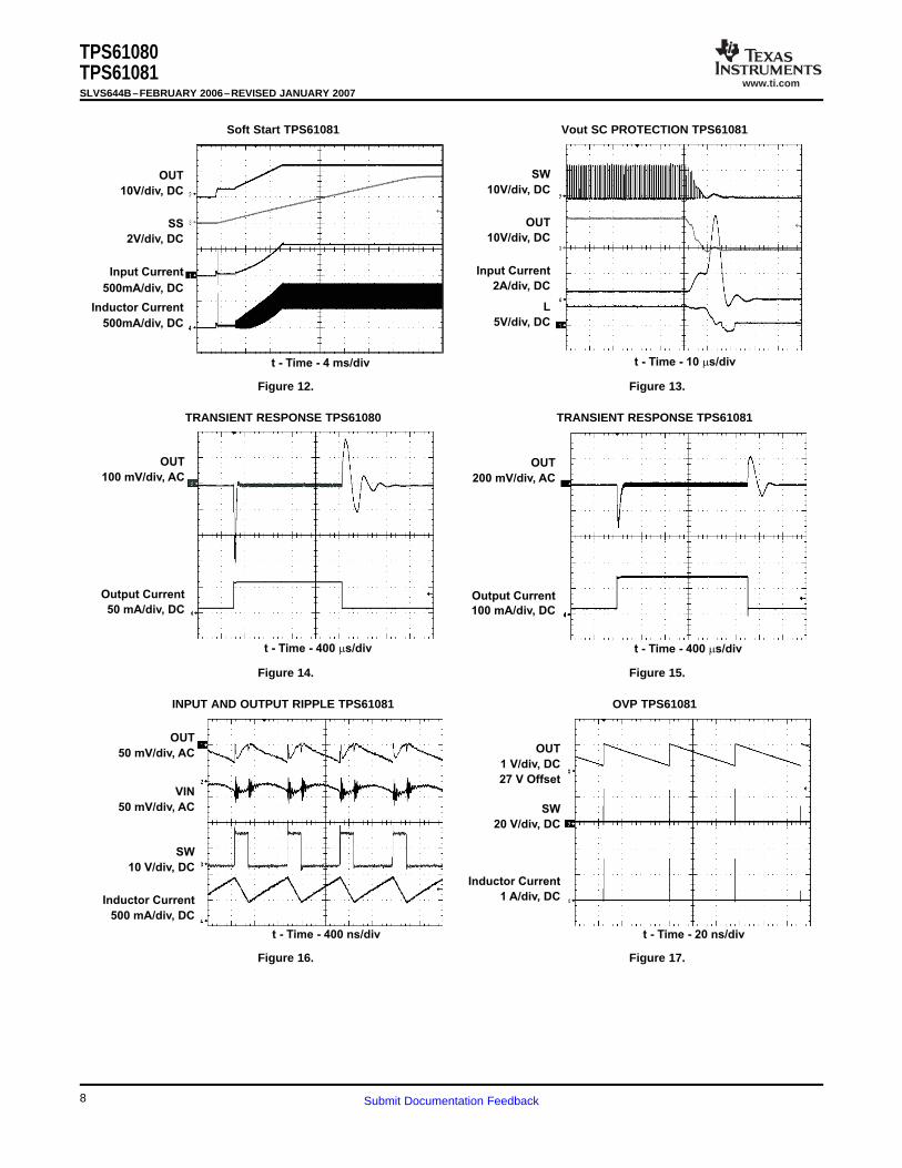
Soft Start TPS61081 Vout SC PROTECTION TPS61081
Figure 12. Figure 13.
TRANSIENT RESPONSE TPS61080 TRANSIENT RESPONSE TPS61081
Figure 14. Figure 15.
INPUT AND OUTPUT RIPPLE TPS61081 OVP TPS61081
Figure 16. Figure 17.
8 Submit Documentation Feedback
www.ti.com
0
0.30
0.60
0.90
1.20
1.50
0 0.30 0.60 0.90 1.20 1.50
SS - Voltage - V
FB
- V
olt
ag
e -
V
V = 3.6 VI
0
0.2
0.4
0.6
0.8
1
1.2
1.4
6 7 8 9 10 11 12V - Output Voltage - VO
I-
Ou
tpu
t C
urr
en
t -
mA
O
V = 3.6 VI
V = 5 VI
TPS61080TPS61081
SLVS644B–FEBRUARY 2006–REVISED JANUARY 2007
SS TO FB ACCURACY TPS61080 MINIMUM LOAD REQUIREMENT TPS61081
Figure 18. Figure 19.
9Submit Documentation Feedback
www.ti.com
DETAILED DESCRIPTION
OPERATION
START UP
OVERCURRENT AND SHORT CIRCUIT PROTECTION
TPS61080TPS61081SLVS644B–FEBRUARY 2006–REVISED JANUARY 2007
TPS61080/1 is a highly integrated boost regulator for up to 27V output. In addition to the on-chip 0.5A/1.2APWM switch and power diode, this IC also builds in an input side isolation switch as shown in the block diagram.One common issue with conventional boost regulator is the conduction path from input to output even whenPWM switch is turned off. It creates three problems, inrush current during start up, output leakage voltage undershutdown, and unlimited short circuit current. To address these issues, TPS61080/1 turns off the isolation switchunder shutdown mode and short circuit condition to eliminate any possible current path. Although the isolationswitch has low RDS(on) for small power losses, shorting the VIN and L pin can bypass the switch and furtherenhance the efficiency.
TPS61080/1 adopts current mode control with constant PWM (pulse width modulation) frequency. The switchingfrequency can be configured to either 600KHz or 1.2MHz through the FSW pin. 600KHz improves light loadefficiency, while 1.2MHz allows using smaller external component. The PWM operation turns on the PWM switchat the beginning of each switching cycle. The input voltage is applied across the inductor and stores the energyas inductor current ramps up. The load current is provided by the output capacitor. When the inductor currentacross the threshold set by error amplifier output, the PWM switch is turned off, and the power diode is forwardbiased. The inductor transfers its stored energy to replenish the output capacitor. This operation repeats in thenext switching cycle.
The error amplifier compares the FB pin voltage with an internal reference, and its output determines the dutycycle of the PWM switching. This close loop system requires loop compensation for stable operation.TPS61080/1 has internal compensation circuitry which accommodates a wide range of input and outputvoltages. The TPS61080/1 integrates slope compensation to the current ramp to avoid the sub-harmonicoscillation that is intrinsic to current mode control schemes.
TPS61080/1 turns on the isolation FET when the EN pin is pulled high, provided that the input voltage is higherthan the undervoltage lockout threshold. The Vgs of the isolation FET is clamped to maintain high on-resistanceand limit the current charging the output capacitor. This feature limits the in-rush current that could pull down theinput supply and cause system instability. Once the output capacitor is charged to VIN, the IC removes the Vgsclamp to fully turn on the isolation FET and at the same time actives soft start by charging the capacitor on theSS pin. If OUT stays lower than VIN-Vsc following a 2ms delay after enable is taken high, the IC recognizes ashort circuit condition. In this case, the isolation FET turns off, and IC remains off until the EN pin toggles or VINcycles through power on reset (POR).
During the soft start phase, the SS pin capacitor is charged by internal bias current of the SS pin. The SS pincapacitor programs the ramp up slope. The SS pin voltage clamps the reference voltage of the FB pin, thereforethe output capacitor rise time follows the SS pin voltage. Without the soft start, the inductor current could reachthe over current limit threshold, and there is potential for output overshoot. see the APPLICATIONINFORMATION section on selecting soft start capacitor values. Pulling the SS pin to ground disables the PWMswitching. However, unlike being disabled by pulling EN low, the IC continues to draw quiescent current and theisolation FET remains on.
TPS61080/1 has a pulse by pulse over current limit feature which turns off the power switch once the inductorcurrent reaches the overcurrent limit. The PWM circuitry resets itself at the beginning of the next switch cycle.The overcurrent threshold determines the available output current. However, the maximum output is also afunction of the input voltage, output voltage, switching frequency and inductor value. Larger inductor values and1.2MHz switching frequency increase the current output capability because of the reduced current ripple. Seethe APPLICATION INFORMATION section for the maximum output current calculation.
In typical boost converter topologies, if the output is grounded, turning off the power switch does not limit thecurrent because a current path exists from the input to output through the inductor and power diode. Toeliminate this path, TPS61080/1 turns off the isolation FET between the input and the inductor. This circuit istriggered when the inductor current remains above short circuit current limit for more than 13µs, or the OUT pinvoltage falls below VIN-1.4V for more than 2ms. An internal catch-diode between the L pin and ground turns onto provide a current discharge path for the inductor. If the short is caused by the output being low, then the IC
10 Submit Documentation Feedback
www.ti.com
OVERVOLTAGE PROTECTION
UNDERVOLTAGE LOCKOUT (UVLO)
THERMAL SHUTDOWN
ENABLE
TPS61080TPS61081
SLVS644B–FEBRUARY 2006–REVISED JANUARY 2007
DETAILED DESCRIPTION (continued)
shuts down and waits for EN to be toggled or a POR. If the short protection is triggered by short circuit currentlimit, the IC attempts to start up one time. After 57ms, the IC restarts in a fashion described in the above section.If the short is cleared, the boost regulator properly starts up and reaches output regulation. However, afterreaching regulation, if another event of short circuit current limit occurs, the IC goes into shutdown mode again,and the fault can only be cleared by toggling the EN pin or POR. Under a permanent short circuit, the IC shutsdown after a start up failure and waits for POR or the EN pin toggling.
The same circuit also protects the ICs and external components when the SW pin is shorted to ground. Thesefeatures provide much more comprehensive and reliable protection than the conventional boost regulator.Table 1 lists the IC protection against the short of each IC pin.
Table 1. TPS61080/1 Short Circuit Protection Mode
SHORTED TO GND FAULT DETECTION IC OPERATION HOW TO CLEAR THE FAULT
IC restarts after 57ms; If it happens again,L, SW INDUCTOR > ISC for 13 µs Turn off isolation FET the fault can only be cleared by toggling
EN or POR.
OUT (during start OUT <Vin– 1.4V for 2 ms IC shuts down Cleared by toggling EN or PORup)
OUT (after start up) OUT <Vin– 1.4V without delay IC shuts down Cleared by toggling EN or POR
EN N/A IC disabled N/A
FSW N/A 600 kHz switching frequency N/A
Disable PWM switching and no output;SS N/A N/Abut still dissipate quiescent current.
Over voltage protection of the OUTFB N/A OUT voltage fails by OVP hysteresispin
GND, PGND, VIN N/A N/A N/A
When TPS61080/1 is configured as regulated current output as shown in the TYPICAL APPLICATIONS, theoutput voltage can run away if the current load is disconnected. The over voltage condition can also occur if theFB pin is shorted to the ground. To prevent the SW node and the output capacitor from exceeding the maximumvoltage rating, an over voltage protection circuit turns off the boost regulator as soon as the output voltageexceeds the OVP threshold. When the output voltage falls 0.7V below the OVP threshold, the regulator resumesthe PWM switching unless the output voltage exceeds the OVP threshold.
An undervoltage lockout prevents mis-operation of the device for input voltages below 1.65 V (typical). When theinput voltage is below the undervoltage threshold, the device remains off and both PWM and isolation switch areturned off, providing isolation between input and output. The undervoltage lockout threshold is set belowminimum operating voltage of 2.5V to avoid any transient VIN dip to trigger UVLO and causes converter reset.For the VIN voltage between UVLO threshold and 2.5V, the IC still maintains its operation. However, the spec isnot assured.
An internal thermal shutdown turns off the isolation and PWM switches when the typical junction temperature of160°C is exceeded. The IC restarts if the junction temperature drops by 15°C.
Connecting the EN pin low turns off the power switch immediately, but keeps the isolation FET on. If the EN pinis logic low for more than 74ms, the IC turns off the isolation FET and enters shutdown mode drawing less than1µA current. The enable input pin has an internal 800kΩ pull down resistor to disable the device when the pin isfloating.
11Submit Documentation Feedback
www.ti.com
FREQUENCY SELECTION
MAXIMUM and MINIMUM OUTPUT CURRENT
Ip 1
L 1VoutVfVin
1Vin Fs
(1)
Iout_max
Vin Ilim Ip2
Vout (2)
Ipeak 2 Iload Vout Vf VinL Fs
D L
IpeakVin
Fs(3)
TPS61080TPS61081SLVS644B–FEBRUARY 2006–REVISED JANUARY 2007
The FSW pin can be connected to either a logic high or logic low to program the switching frequency to1.2MHzor 600kHz respectively. The 600kHz switching frequency provides better efficiency because of lower switchinglosses. This advantage becomes more evident at light load when switching losses dominate overall losses. Thehigher switching frequency shrinks external component size and thus the size of power solution. High switchingfrequency also improves load transient response since the smaller value inductor takes less time to ramp up anddown current. The other benefits of high switching frequency are lower output ripples and a higher maximumoutput current. Overall, it is recommended to use 1.2MHz switching frequency unless light load efficiency is amajor concern.
The FSW pin has internal 800kΩ pull up resistor to the VIN pin. Floating this pin programs the switchingfrequency to 1.2MHz.
The over-current limit in a boost converter limits the maximum input current and thus maximum input power froma given input voltage. Maximum output power is less than maximum input power due to power conversionlosses. Therefore, the over-current limit, the input voltage, the output voltage and the conversion efficiency allaffect maximum current output. Since the over-current limit clamps the peak inductor current, the current ripplehas to be subtracted to derive maximum DC current. The current ripple is a function of the switching frequency,the inductor value and the duty cycle.
whereIp = inductor peak to peak rippleL = inductor valueVf = power diode forward voltageFs = Switching frequency
The following equations take into account of all the above factors for maximum output current calculation.
whereIlim = overcurrent limitη = conversion efficiency
To minimize the variation in the overcurrent limit threshold, the TPS61080/1 uses the VIN and OUT pin voltageto compensate for the variation caused by the slope compensation. However, the threshold still has somedependency on the VIN and OUT voltage. Use Figure 6 to Figure 9 to identify the typical over-current limit inyour application, and use 25% tolerance to account for temperature dependency and process variations.
Because of the minimum duty cycle of each power switching cycle of TPS61080/1, the device can loseregulation at the very light load. Use the following equations to calculate PWM duty cycle under discontinuesconduction mode (DCM).
WhereIpeak = inductor peak to peak ripple in DCMIload = load currentD = PWM switching duty cycle
12 Submit Documentation Feedback

www.ti.com
TPS61080TPS61081
SLVS644B–FEBRUARY 2006–REVISED JANUARY 2007
If the calculated duty cycle is less than 5%, minimum load should be considered to the boost output to ensureregulation. Figure 19 provides quick reference to identify the minimum load requirements for two input voltages.
13Submit Documentation Feedback
www.ti.com
APPLICATION INFORMATION
PROGRAM OUTPUT VOLTAGE
TPS61080/1
OUT
FB
R1
R2
C 1
R3
100 W
C2
4.7 Fm
R1 R2 Vout1.229V
1(4)
FEED FORWARD CAPACITOR
Fz1
2R1 C1 (5)
FP 1R1
1R2 1
2C1 (6)
FP1
2R2C1when R1 R2.
(7)
TPS61080TPS61081SLVS644B–FEBRUARY 2006–REVISED JANUARY 2007
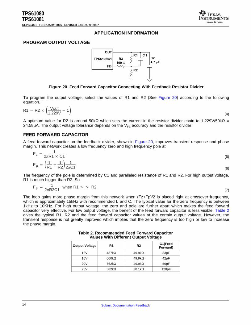
Figure 20. Feed Forward Capacitor Connecting With Feedback Resistor Divider
To program the output voltage, select the values of R1 and R2 (See Figure 20) according to the followingequation.
A optimum value for R2 is around 50kΩ which sets the current in the resistor divider chain to 1.229V/50kΩ =24.58µA. The output voltage tolerance depends on the VFB accuracy and the resistor divider.
A feed forward capacitor on the feedback divider, shown in Figure 20, improves transient response and phasemargin. This network creates a low frequency zero and high frequency pole at
The frequency of the pole is determined by C1 and paralleled resistance of R1 and R2. For high output voltage,R1 is much bigger than R2. So
The loop gains more phase margin from this network when (Fz+Fp)/2 is placed right at crossover frequency,which is approximately 15kHz with recommended L and C. The typical value for the zero frequency is between1kHz to 10KHz. For high output voltage, the zero and pole are further apart which makes the feed forwardcapacitor very effective. For low output voltage, the benefit of the feed forward capacitor is less visible. Table 2gives the typical R1, R2 and the feed forward capacitor values at the certain output voltage. However, thetransient response is not greatly improved which implies that the zero frequency is too high or low to increasethe phase margin.
Table 2. Recommended Feed Forward CapacitorValues With Different Output Voltage
C1(FeedOutput Voltage R1 R2 Forward)
12V 437kΩ 49.9kΩ 33pF
16V 600kΩ 49.9kΩ 42pF
20V 762kΩ 49.9kΩ 56pF
25V 582kΩ 30.1kΩ 120pF
14 Submit Documentation Feedback
www.ti.com
SOFT START CAPACITOR
tssCss 1.229
Iss (8)
Iin_cout CoutIss Vout
Css Vin (9)
Iin_ss Iin_coutVout
Vin Iload
(10)
Kref K2Vclp K2
Iss K2R
(11)
INDUCTOR SELECTION
TPS61080TPS61081
SLVS644B–FEBRUARY 2006–REVISED JANUARY 2007
The 100Ω resistor is added to reduce noise coupling from the OUT to the FB pin through the feed forwardcapacitor. Without the resistor, the regulator may oscillate at high output current.
The voltage at the SS pin clamps the internal reference voltage, which allows the output voltage to ramp upslowly. The soft start time is calculated as
whereCss = soft start capacitorIss = soft start bias current (TYP 5 µA)1.229V is the typical value of the reference voltage.
During start up, input current has to be supplied to charge the output capacitor. This current is proportional torising slope of the output voltage, and peaks when output reaches regulation.
WhereIin_cout = additional input current for charging the output capacitor
The maximum input during soft start is
Output overshoot can occur if the input current at startup exceeds the inductor saturation current and/or reachescurrent limit because the error amplifier loses control of the voltage feedback loop. The in-rush current can alsopull down input sources, potentially causing system reset. Therefore, select Css to make Iin_ss stay below theinductor saturation current, the IC over current limit and the input's maximum supply current.
TPS61080/1 can also be configured for constant current output, as shown in the typical applications. In thisconfiguration, a current sense resistor is connected to FB pin for output current regulation. In order to reducepower loss on the sense resistor, FB pin reference voltage can be lowered by connecting a resistor to the SS pinThe new reference voltage is simply the resistor value times the SS pin bias current. However, keep in mind thatthis reference has higher tolerance due to the tolerance of the bias current and sense resistor, and the offset ofthe clamp circuit. Refer to the specification VCLP and ISS to calculate the tolerance as following.
WhereKref = percentage tolerance of the FB reference voltage.KVclp = percentage tolerance of the clamp circuit.Klss = percentage tolerance of the SS pin bias current.KR = percentage tolerance of the SS pin resistor.
Without considering the SS pin resistor tolerance, the FB reference voltage has ±5.6% under the roomtemperature.
Because the selection of the inductor affects steady state operation, transient behavior and loop stability, theinductor is the most important component in power regulator design. There are three important inductorspecifications, inductor value, DC resistance and saturation current. Considering inductor value alone is notenough.
15Submit Documentation Feedback
www.ti.com
IL_DCVout Iout
Vin (12)
INPUT AND OUTPUT CAPACITOR SELECTION
Cout Vout Vin
IoutVout Fs Vripple (13)
Vripple_ESR Iout RESR (14)
TPS61080TPS61081SLVS644B–FEBRUARY 2006–REVISED JANUARY 2007
The inductor's inductance value determines the inductor ripple current. It is generally recommended to set peakto peak ripple current given by Equation 4 to 30–40% of DC current. Also, the inductor value should not bebeyond the range in the recommended operating conditions table. It is a good compromise of power losses andinductor size. Inductor DC current can be calculated as
The internal loop compensation for PWM control is optimized for the external component shown in the typicalapplication circuit with consideration of component tolerance. Inductor values can have ±20% tolerance with nocurrent bias. When the inductor current approaches saturation level, its inductance can decrease 20% to 35%from the 0A value depending on how the inductor vendor defines saturation current. Using an inductor with asmaller inductance value forces discontinuous PWM in which inductor current ramps down to zero before theend of each switching cycle. It reduces the boost converter’s maximum output current, causes large inputvoltage ripple and reduces efficiency. An inductor with larger inductance reduces the gain and phase margin ofthe feedback loop, possibly resulting in instability.
For these reasons, 10µH inductors are recommended for TPS61080 and 4.7µH inductors for TPS61081 for mostapplications. However, 10µH inductor is also suitable for 600kHz switching frequency.
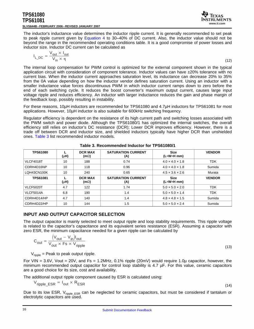
Regulator efficiency is dependent on the resistance of its high current path and switching losses associated withthe PWM switch and power diode. Although the TPS61080/1 has optimized the internal switches, the overallefficiency still relies on inductor’s DC resistance (DCR); Lower DCR improves efficiency. However, there is atrade off between DCR and inductor size, and shielded inductors typically have higher DCR than unshieldedones. Table 3 list recommended inductor models.
Table 3. Recommended Inductor for TPS61080/1
TPS61080 L DCR MAX SATURATION CURRENT Size VENDOR(µH) (mΩ) (A) (L×W×H mm)
VLCF4018T 10 188 0.74 4.0 × 4.0 × 1.8 TDK
CDRH4D16NP 10 118 0.96 4.0 × 4.0 × 1.8 Sumida
LQH43CN100K 10 240 0.65 4.5 × 3.6 × 2.6 Murata
TPS61081 L DCR MAX SATURATION CURRENT Size VENDOR(µH) (mΩ) (A) (L×W×H mm)
VLCF5020T 4.7 122 1.74 5.0 × 5.0 × 2.0 TDK
VLCF5014A 6.8 190 1.4 5.0 × 5.0 × 1.4 TDK
CDRH4D14/HP 4.7 140 1.4 4.8 × 4.8 × 1.5 Sumida
CDRH4D22/HP 10 144 1.5 5.0 × 5.0 × 2.4 Sumida
The output capacitor is mainly selected to meet output ripple and loop stability requirements. This ripple voltageis related to the capacitor’s capacitance and its equivalent series resistance (ESR). Assuming a capacitor withzero ESR, the minimum capacitance needed for a given ripple can be calculated by
Vripple = Peak to peak output ripple.
For VIN = 3.6V, Vout = 20V, and Fs = 1.2MHz, 0.1% ripple (20mV) would require 1.0µ capacitor, however, theminimum recommended output capacitor for control loop stability is 4.7 µF. For this value, ceramic capacitorsare a good choice for its size, cost and availability.
The additional output ripple component caused by ESR is calculated using:
Due to its low ESR, Vripple_ESR can be neglected for ceramic capacitors, but must be considered if tantalum orelectrolytic capacitors are used.
16 Submit Documentation Feedback
www.ti.com
LAYOUT CONSIDERATION
FSW
Vout
EN
GND
Th
erm
al
Pa
dCs
C1
R1
R2
C3*
C2
L1Vin
R3*
PGND
TPS61080TPS61081
SLVS644B–FEBRUARY 2006–REVISED JANUARY 2007
During a load transient, the output capacitor at the output of the boost converter has to supply or absorbtransient current before the inductor current ramps up its steady state value. Larger capacitors always help toreduce the voltage over and under shoot during a load transient. A larger capacitor also helps loop stability.Care must be taken when evaluating a ceramic capacitor’s derating under dc bias, aging and AC signal. Forexample, larger form factor capacitors (in 1206 size) have their self resonant frequencies in the range of theswitching frequency. So the effective capacitance is significantly lower. The Dc bias can also significantly reducecapacitance. Ceramic capacitors can loss as much as 50% of its capacitance at its rated voltage. Therefore,almost leave margin on voltage rating to ensure adequate capacitance.
The popular vendors for high value ceramic capacitors are:TDK (http://www.component.tdk.com/components.php)Murata (http://www.murata.com/cap/index.html)
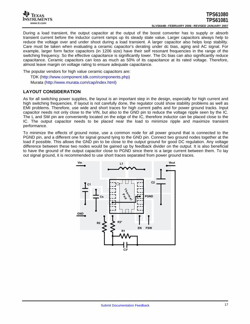
As for all switching power supplies, the layout is an important step in the design, especially for high current andhigh switching frequencies. If layout is not carefully done, the regulator could show stability problems as well asEMI problems. Therefore, use wide and short traces for high current paths and for power ground tracks. Inputcapacitor needs not only close to the VIN, but also to the GND pin to reduce the voltage ripple seen by the IC.The L and SW pin are conveniently located on the edge of the IC, therefore inductor can be placed close to theIC. The output capacitor needs to be placed near the load to minimize ripple and maximize transientperformance.
To minimize the effects of ground noise, use a common node for all power ground that is connected to thePGND pin, and a different one for signal ground tying to the GND pin. Connect two ground nodes together at theload if possible. This allows the GND pin to be close to the output ground for good DC regulation. Any voltagedifference between these two nodes would be gained up by feedback divider on the output. It is also beneficialto have the ground of the output capacitor close to PGND since there is a large current between them. To layout signal ground, it is recommended to use short traces separated from power ground traces.
17Submit Documentation Feedback
www.ti.com
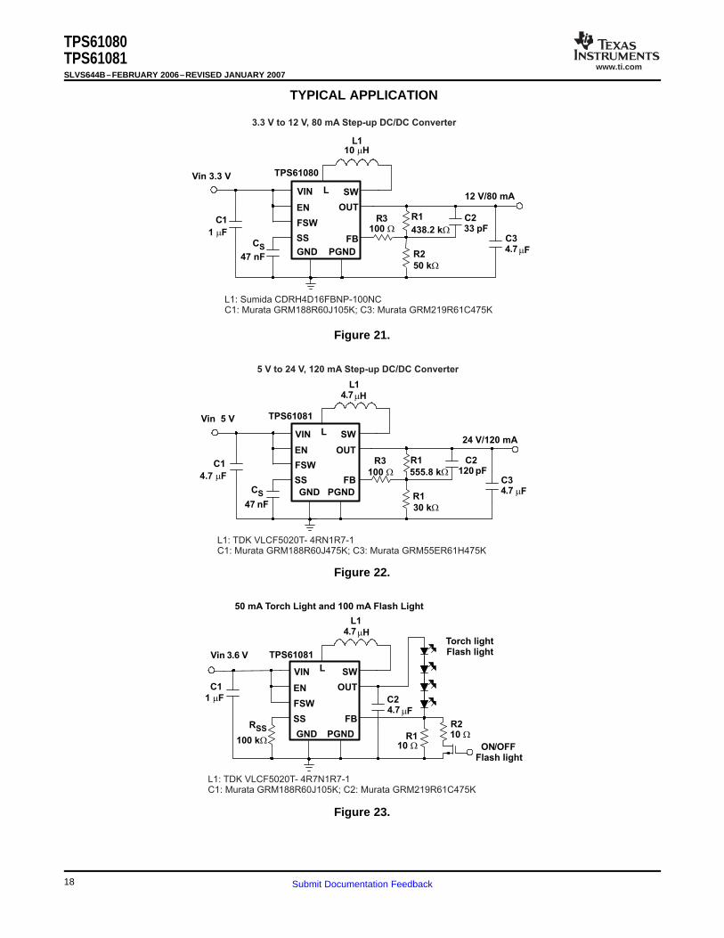
TYPICAL APPLICATION
Vin 3.3 V
L110 Hm
C1
1 Fm
C233 pF
12 V/80 mAVIN
PGND
L SW
OUT
FBSS
GND
EN
FSWR1
438.2 kW
CS
47 nF
R3100 W
R2
50 kW
TPS61080
C34.7mF
3.3 V to 12 V, 80 mA Step-up DC/DC Converter
L1: Sumida CDRH4D16FBNP-100NC
C1: Murata GRM188R60J105K; C3: Murata GRM219R61C475K
Vin 5 V
L14.7mH
C1
4.7 Fm
C2120 pF
24 V/120 mAVIN
PGND
L SW
OUT
FBSS
GND
EN
FSWR1
555.8 kW
CS
47 nF
R3
100 W
R1
30 kW
C34.7 mF
TPS61081
5 V to 24 V, 120 mA Step-up DC/DC Converter
L1: TDK VLCF5020T- 4RN1R7-1
C1: Murata GRM188R60J475K; C3: Murata GRM55ER61H475K
Vin 3.6 V
L14.7mH
C1
1 Fm C24.7 mF
Torch lightFlash light
VIN
PGND
L SW
OUT
FBSS
GND
EN
FSW
R110 W
RSS
100 kWON/OFF
Flash light
R210 W
TPS61081
50 mA Torch Light and 100 mA Flash Light
L1: TDK VLCF5020T- 4R7N1R7-1
C1: Murata 188R60J105K; C2: Murata GRM219R61C475KGRM
TPS61080TPS61081SLVS644B–FEBRUARY 2006–REVISED JANUARY 2007
Figure 21.
Figure 22.
Figure 23.
18 Submit Documentation Feedback
www.ti.com
Vin 5 V
L14.7 mH
C1
4. 7mF C24.7mF
10.5V/200 mA
VIN
PGND
L SW
OUT
FBSS
GND
EN
FSW
10 strings
Rset
1 W
R1
PWMSignal
R2
80 kW
TPS61081
30 WLEDs Driver in Media Factor Form Display
80 kW
L1: TDK VLCF5020T- 4R7N1R7-1
C1: Murata 188R60J475K; C2: Murata GRM219R61C475KGRM
Vin 5 V
L110 mH
C14.7 mF
C34.7 mF
15V/30mAVIN
PGND
L SW
OUT
FBSS
GND
EN
FSWR1560.3 KW
Cs20nF
R150 KW
C20.1 mF D1 D2
-15V/30mA
TPS61080
+/ – 15 V Dual Output Converter
C44.7 mF
L1: Sumida CDRH4D16NP-100NC
C1: Murata 188R60J475K; C3,C4: Murata GRM219R61C475K
D1,D2: ON Semiconductor MBR0520
GRM
Vin 5V
L14.7 mH
C14.7mF
C44.7mFVIN
PGND
L SW
OUT
FBSS
GND
EN
FSW
R1794 KW
Cs20nF
R220 KW
C21 mF
D1 D2
50V/50mA
C34.7mF
TPS61081
5 V to 50 V,50 mA Step-up DC/DC Converter with Output Doubler
L1: TDK VLCF5020T-4R7N1R7-1
C1: Murata 188R60J475K; C3: Murata GRM219R61C475K
D1,D2: ON Semiconductor MBR0520
GRM
TPS61080TPS61081
SLVS644B–FEBRUARY 2006–REVISED JANUARY 2007
TYPICAL APPLICATION (continued)
Figure 24.
Figure 25.
Figure 26.
19Submit Documentation Feedback

IMPORTANT NOTICE
Texas Instruments Incorporated and its subsidiaries (TI) reserve the right to make corrections, modifications, enhancements, improvements, and other changes to its products and services at any time and to discontinue any product or service without notice. Customers should obtain the latest relevant information before placing orders and should verify that such information is current and complete. All products are sold subject to TI’s terms and conditions of sale supplied at the time of order acknowledgment. TI warrants performance of its hardware products to the specifications applicable at the time of sale in accordance with TI’s standard warranty. Testing and other quality control techniques are used to the extent TI deems necessary to support this warranty. Except where mandated by government requirements, testing of all parameters of each product is not necessarily performed. TI assumes no liability for applications assistance or customer product design. Customers are responsible for their products and applications using TI components. To minimize the risks associated with customer products and applications, customers should provide adequate design and operating safeguards. TI does not warrant or represent that any license, either express or implied, is granted under any TI patent right, copyright, mask work right, or other TI intellectual property right relating to any combination, machine, or process in which TI products or services are used. Information published by TI regarding third-party products or services does not constitute a license from TI to use such products or services or a warranty or endorsement thereof. Use of such information may require a license from a third party under the patents or other intellectual property of the third party, or a license from TI under the patents or other intellectual property of TI. Reproduction of information in TI data books or data sheets is permissible only if reproduction is without alteration and is accompanied by all associated warranties, conditions, limitations, and notices. Reproduction of this information with alteration is an unfair and deceptive business practice. TI is not responsible or liable for such altered documentation. Resale of TI products or services with statements different from or beyond the parameters stated by TI for that product or service voids all express and any implied warranties for the associated TI product or service and is an unfair and deceptive business practice. TI is not responsible or liable for any such statements. Following are URLs where you can obtain information on other Texas Instruments products and application solutions: Products Applications Amplifiers amplifier.ti.com Audio www.ti.com/audio Data Converters dataconverter.ti.com Automotive www.ti.com/automotive DSP dsp.ti.com Broadband www.ti.com/broadband Interface interface.ti.com Digital Control www.ti.com/digitalcontrol Logic logic.ti.com Military www.ti.com/military Power Mgmt power.ti.com Optical Networking www.ti.com/opticalnetwork Microcontrollers microcontroller.ti.com Security www.ti.com/security Low Power Wireless www.ti.com/lpw Telephony www.ti.com/telephony Video & Imaging www.ti.com/video Wireless www.ti.com/wireless Mailing Address: Texas Instruments Post Office Box 655303 Dallas, Texas 75265
Copyright © 2007, Texas Instruments Incorporated