HIGH PRECISION, LOW NOISE OPERATIONAL … · SBOS594A – MARCH 2012– REVISED NOVEMBER 2012
23
1 2 3 4 8 7 6 5 V+ Out B –In B +In B Out A –In A +In A V– A B D PACKAGE (TOP VIEW) OPA2227-EP www.ti.com SBOS594A – MARCH 2012 – REVISED NOVEMBER 2012 HIGH PRECISION, LOW NOISE OPERATIONAL AMPLIFIER Check for Samples: OPA2227-EP 1FEATURES • Low Noise: 3 nV/√Hz SUPPORTS DEFENSE, AEROSPACE, AND MEDICAL APPLICATIONS • Wide Bandwidth: 8 MHz, 2.3 V/μs • Controlled Baseline • Settling Time: 5 μs • One Assembly and Test Site • High CMRR: 138 dB (Typical) • One Fabrication Site • High Open-Loop Gain: 160 dB (Typical) • Available in Military (–55°C to 125°C) • Low Input Bias Current: 10 nA Maximum at Temperature Range (1) 25°C • Extended Product Life Cycle • Low Offset Voltage: 100 μV Maximum at 25°C • Extended Product-Change Notification • Wide Supply Range: ±2.5 V to ±18 V • Product Traceability APPLICATIONS • Data Acquisition • Telecom Equipment • Geophysical Analysis • Vibration Analysis • Spectral Analysis • Professional Audio Equipment • Active Filters • Power Supply Control (1) Additional temperature ranges available - contact factory DESCRIPTION The OPA2227 operational amplifier combines low noise and wide bandwidth with high precision to make it the ideal choice for applications requiring both ac and precision dc performance. The OPA2227 is unity-gain stable and features high slew rate (2.3 V/μs) and wide bandwidth (8 MHz). The OPA2227 operational amplifier is ideal for professional audio equipment. In addition, low quiescent current and low cost make them ideal for portable applications requiring high precision. The OPA2227 operational amplifier is a pin-for-pin replacement for the industry standard OP-27 with substantial improvements across the board. The dual and quad versions are available for space savings and perchannel cost reduction. The OPA2227 is available in an SOIC-8 package. Operation is specified from –55°C to 125°C. 1 Please be aware that an important notice concerning availability, standard warranty, and use in critical applications of Texas Instruments semiconductor products and disclaimers thereto appears at the end of this data sheet. PRODUCTION DATA information is current as of publication date. Copyright © 2012, Texas Instruments Incorporated Products conform to specifications per the terms of the Texas Instruments standard warranty. Production processing does not necessarily include testing of all parameters.
Transcript of HIGH PRECISION, LOW NOISE OPERATIONAL … · SBOS594A – MARCH 2012– REVISED NOVEMBER 2012
1
2
3
4
8
7
6
5
V+
Out B
–In B
+In B
Out A
–In A
+In A
V–
A
B
D PACKAGE(TOP VIEW)
OPA2227-EP
www.ti.com SBOS594A –MARCH 2012–REVISED NOVEMBER 2012
HIGH PRECISION, LOW NOISE OPERATIONAL AMPLIFIERCheck for Samples: OPA2227-EP
1FEATURES• Low Noise: 3 nV/√Hz SUPPORTS DEFENSE, AEROSPACE,
AND MEDICAL APPLICATIONS• Wide Bandwidth: 8 MHz, 2.3 V/μs• Controlled Baseline• Settling Time: 5 μs• One Assembly and Test Site• High CMRR: 138 dB (Typical)• One Fabrication Site• High Open-Loop Gain: 160 dB (Typical)• Available in Military (–55°C to 125°C)• Low Input Bias Current: 10 nA Maximum at
Temperature Range (1)25°C• Extended Product Life Cycle• Low Offset Voltage: 100 μV Maximum at 25°C• Extended Product-Change Notification• Wide Supply Range: ±2.5 V to ±18 V• Product Traceability
APPLICATIONS• Data Acquisition• Telecom Equipment• Geophysical Analysis• Vibration Analysis• Spectral Analysis• Professional Audio Equipment• Active Filters• Power Supply Control (1) Additional temperature ranges available - contact factory
DESCRIPTIONThe OPA2227 operational amplifier combines low noise and wide bandwidth with high precision to make it theideal choice for applications requiring both ac and precision dc performance.
The OPA2227 is unity-gain stable and features high slew rate (2.3 V/μs) and wide bandwidth (8 MHz).
The OPA2227 operational amplifier is ideal for professional audio equipment. In addition, low quiescent currentand low cost make them ideal for portable applications requiring high precision.
The OPA2227 operational amplifier is a pin-for-pin replacement for the industry standard OP-27 with substantialimprovements across the board. The dual and quad versions are available for space savings and perchannelcost reduction.
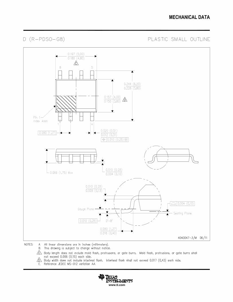
The OPA2227 is available in an SOIC-8 package. Operation is specified from –55°C to 125°C.
1
Please be aware that an important notice concerning availability, standard warranty, and use in critical applications ofTexas Instruments semiconductor products and disclaimers thereto appears at the end of this data sheet.
PRODUCTION DATA information is current as of publication date. Copyright © 2012, Texas Instruments IncorporatedProducts conform to specifications per the terms of the TexasInstruments standard warranty. Production processing does notnecessarily include testing of all parameters.
OPA2227-EP
SBOS594A –MARCH 2012–REVISED NOVEMBER 2012 www.ti.com
This integrated circuit can be damaged by ESD. Texas Instruments recommends that all integrated circuits be handled withappropriate precautions. Failure to observe proper handling and installation procedures can cause damage.
ESD damage can range from subtle performance degradation to complete device failure. Precision integrated circuits may be moresusceptible to damage because very small parametric changes could cause the device not to meet its published specifications.
ORDERING INFORMATION (1)
ORDERABLE PARTTA PACKAGE TOP-SIDE MARKING VID NUMBER TRANSPORT MEDIANUMBER
OPA2227MDREP V62/12610-01XE Tape and Reel, large–55°C to SOIC-8 – D 2227EP125°C OPA2227MDEP V62/12610-01XE-T Tube
(1) For the most current package and ordering information, see the Package Option Addendum at the end of this document, or see the TIwebsite at www.ti.com.
ABSOLUTE MAXIMUM RATINGS (1)
over operating free-air temperature range (unless otherwise noted)
VALUE UNIT
Supply voltage ±18 V
Signal input terminals Voltage (V–) – 0.7 to (V+) + 0.7 V
Current 20 mA
Output short-circuit (to ground) (2) Continuous
Operating temperature -55 to 125 °C
Storage temperature -65 to 150 °C
Junction temperature 150 °C
Lead temperature (soldering, 10 s) 300 °C
(1) Stresses beyond those listed under "absolute maximum ratings" may cause permanent damage to the device. These are stress ratingsonly, and functional operation of the device at these or any other conditions beyond those indicated under "recommended operatingconditions" is not implied. Exposure to absolute-maximum-rated conditions for extended periods may affect device reliability.
(2) One channel per package.
THERMAL INFORMATIONOPA2227
THERMAL METRIC (1) D UNITS
8 PINS
θJA Junction-to-ambient thermal resistance (2) 91.9
θJCtop Junction-to-case (top) thermal resistance (3) 39.9
θJB Junction-to-board thermal resistance (4) 40.6°C/W
ψJT Junction-to-top characterization parameter (5) 3.9
ψJB Junction-to-board characterization parameter (6) 39.6
θJCbot Junction-to-case (bottom) thermal resistance (7) N/A
(1) For more information about traditional and new thermal metrics, see the IC Package Thermal Metrics application report, SPRA953.(2) The junction-to-ambient thermal resistance under natural convection is obtained in a simulation on a JEDEC-standard, high-K board, as
specified in JESD51-7, in an environment described in JESD51-2a.(3) The junction-to-case (top) thermal resistance is obtained by simulating a cold plate test on the package top. No specific JEDEC-
standard test exists, but a close description can be found in the ANSI SEMI standard G30-88.(4) The junction-to-board thermal resistance is obtained by simulating in an environment with a ring cold plate fixture to control the PCB
temperature, as described in JESD51-8.(5) The junction-to-top characterization parameter, ψJT, estimates the junction temperature of a device in a real system and is extracted
from the simulation data for obtaining θJA, using a procedure described in JESD51-2a (sections 6 and 7).(6) The junction-to-board characterization parameter, ψJB, estimates the junction temperature of a device in a real system and is extracted
from the simulation data for obtaining θJA , using a procedure described in JESD51-2a (sections 6 and 7).(7) The junction-to-case (bottom) thermal resistance is obtained by simulating a cold plate test on the exposed (power) pad. No specific
JEDEC standard test exists, but a close description can be found in the ANSI SEMI standard G30-88.Spacer
2 Submit Documentation Feedback Copyright © 2012, Texas Instruments Incorporated
Product Folder Links: OPA2227-EP
OPA2227-EP
www.ti.com SBOS594A –MARCH 2012–REVISED NOVEMBER 2012
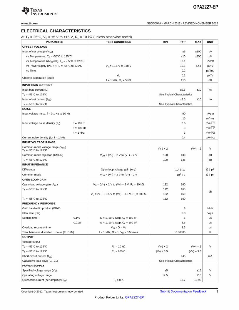
ELECTRICAL CHARACTERISTICSAt TA = 25°C, VS = ±5 V to ±15 V, RL = 10 kΩ (unless otherwise noted).
PARAMETER TEST CONDITIONS MIN TYP MAX UNIT
OFFSET VOLTAGE
Input offset voltage (VOS) ±5 ±100 µV
vs Temperature, TA = -55°C to 125°C ±10 ±250 µV
vs Temperature (dVOS/dT), TA = -55°C to 125°C ±0.1 µV/°C
vs Power supply (PSRR) TA = -55°C to 125°C VS = ±2.5 V to ±18 V ±0.5 ±2.1 µV/V
vs Time 0.2 µV/mo
dc 0.2 µV/VChannel separation (dual)
f = 1 kHz, RL = 5 kΩ 110 dB
INPUT BIAS CURRENT
Input bias current (IB) ±2.5 ±10 nA
TA = -55°C to 125°C See Typical Characteristics
Input offset current (IOS) ±2.5 ±10 nA
TA = -55°C to 125°C See Typical Characteristics
NOISE
Input voltage noise, f = 0.1 Hz to 10 Hz 90 nVp-p
15 nVrms
Input voltage noise density (en) f = 10 Hz 3.5 nV/√Hz
f = 100 Hz 3 nV/√Hz
f = 1 kHz 3 nV/√Hz
Current noise density (in), f = 1 kHz 0.4 pA/√Hz
INPUT VOLTAGE RANGE
Common-mode voltage range (VCM) (V-) + 2 (V+) – 2 VTA = -55°C to 125°C
Common-mode rejection (CMRR) VCM = (V–) + 2 V to (V+) – 2 V 120 138 dB
TA = -55°C to 125°C 108 138 dB
INPUT IMPEDANCE
Differential Open-loop voltage gain (AOL) Ω || pF107 || 12
Common-mode VCM = (V–) + 2 V to (V+) – 2 V Ω || pF109 || 3
OPEN-LOOP GAIN
Open-loop voltage gain (AOL) VO = (V–) + 2 V to (V+) – 2 V, RL = 10 kΩ 132 160
TA = -55°C to 125°C 112 160dB
VO = (V–) + 3.5 V to (V+) – 3.5 V, RL = 600 Ω 132 160
TA = -55°C to 125°C 112 160
FREQUENCY RESPONSE
Gain bandwidth product (GBW) 8 MHz
Slew rate (SR) 2.3 V/µs
Settling time: 0.1% G = 1, 10-V Step, CL = 100 pF 5 µs
0.01% G = 1, 10-V Step, CL = 100 pF 5.6 µs
Overload recovery time VIN x G = VS 1.3 µs
Total harmonic distortion + noise (THD+N) f = 1 kHz, G = 1, VO = 3.5 Vrms 0.00005 %
OUTPUT
Voltage output
TA = -55°C to 125°C RL = 10 kΩ (V-) + 2 (V+) – 2 V
TA = -55°C to 125°C RL = 600 Ω (V-) + 3.5 (V+) – 3.5
Short-circuit current (ISC) ±45 mA
Capacitive load drive (CLOAD) See Typical Characteristics
POWER SUPPLY
Specified voltage range (VS) ±5 ±15 V
Operating voltage range ±2.5 ±18 V
Quiescent current (per amplifier) (IQ) IO = 0 A ±3.7 ±3.95
Copyright © 2012, Texas Instruments Incorporated Submit Documentation Feedback 3
Product Folder Links: OPA2227-EP
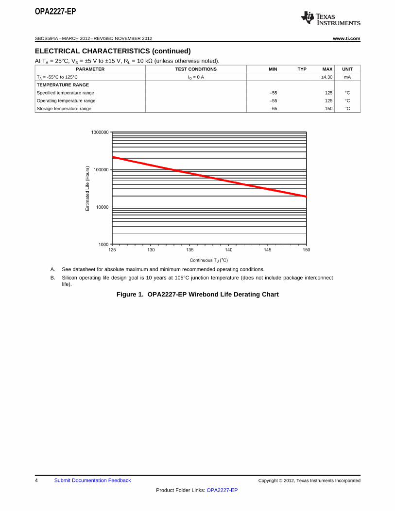
1000
10000
100000
1000000
125 130 135 140 145 150
Estim
ate
d L
ife
(H
ou
rs)
Continuous TJ (°C)
OPA2227-EP
SBOS594A –MARCH 2012–REVISED NOVEMBER 2012 www.ti.com
ELECTRICAL CHARACTERISTICS (continued)At TA = 25°C, VS = ±5 V to ±15 V, RL = 10 kΩ (unless otherwise noted).
PARAMETER TEST CONDITIONS MIN TYP MAX UNIT
TA = -55°C to 125°C IO = 0 A ±4.30 mA
TEMPERATURE RANGE
Specified temperature range –55 125 °C
Operating temperature range –55 125 °C
Storage temperature range –65 150 °C
xxx
A. See datasheet for absolute maximum and minimum recommended operating conditions.
B. Silicon operating life design goal is 10 years at 105°C junction temperature (does not include package interconnectlife).
Figure 1. OPA2227-EP Wirebond Life Derating Chart
4 Submit Documentation Feedback Copyright © 2012, Texas Instruments Incorporated
Product Folder Links: OPA2227-EP
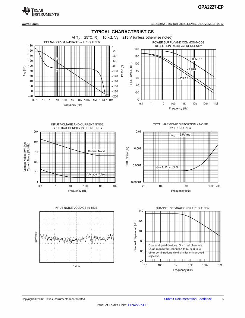
20 100 1k 10k 20k
0.01
0.001
0.0001
0.00001
TH
D+
No
ise (
%)
Frequency (Hz)
TOTAL HARMONIC DISTORTION + NOISE
vs FREQUENCY
G = 1, RL = 10kΩ
VOUT = 3.5Vrms
0.01 0.10 1 10 100 1k 10k 100k 1M 10M 100M
180
160
140
120
100
80
60
40
20
0
–20
AO
L(d
B)
0
–20
–40
–60
–80
–100
–120
–140
–160
–180
–200
Ph
ase
(°)
Frequency (Hz)
OPEN-LOOP GAIN/PHASE vs FREQUENCY
G
φ
10.1 10 100 1k 10k 100k 1M
140
120
100
80
60
40
-20
–0
PS
RR
, C
MR
R (
dB
)
Frequency (Hz)
POWER SUPPLY AND COMMON-MODE
REJECTION RATIO vs FREQUENCY
+CMRR
+PSRR
–PSRR
0.1 101 100 1k 10k
100k
10k
1k
100
10
1
Vo
ltag
e N
ois
e (
nV
/√H
z)
Cu
rre
nt N
ois
e (
fA/√
Hz)
Frequency (Hz)
INPUT VOLTAGE AND CURRENT NOISE
SPECTRAL DENSITY vs FREQUENCY
Current Noise
Voltage Noise
10 100 1k 10k 100k 1M
140
120
100
80
60
40
Ch
an
ne
l S
ep
ara
tio
n (
dB
)
Frequency (Hz)
CHANNEL SEPARATION vs FREQUENCY
Dual and quad devices. G = 1, all channels.
Quad measured Channel A to D, or B to C;
other combinations yield similiar or improved
rejection.
INPUT NOISE VOLTAGE vs TIME
1s/div
50
nV
/div
OPA2227-EP
www.ti.com SBOS594A –MARCH 2012–REVISED NOVEMBER 2012
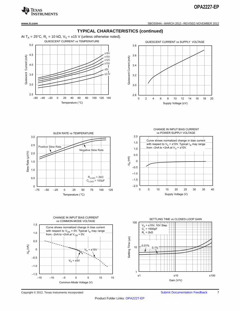
TYPICAL CHARACTERISTICSAt TA = 25°C, RL = 10 kΩ, VS = ±15 V (unless otherwise noted).
Copyright © 2012, Texas Instruments Incorporated Submit Documentation Feedback 5
Product Folder Links: OPA2227-EP
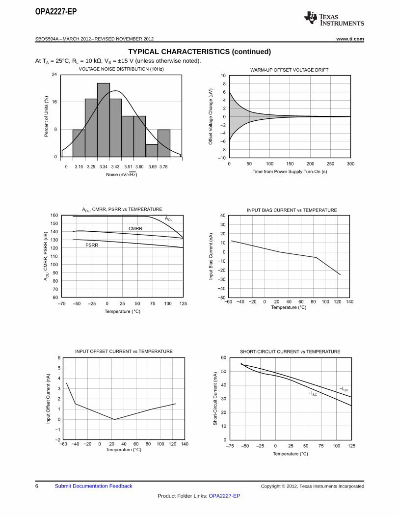
10
8
6
4
2
0
–2
–4
–6
–8
–10
Offse
t V
olta
ge C
ha
ng
e (
µV
)
0 100 150 300
Time from Power Supply Turn-On (s)
WARM-UP OFFSET VOLTAGE DRIFT
50 200 250
VOLTAGE NOISE DISTRIBUTION (10Hz)
Perc
en
t of U
nits (
%)
Noise (nV/√Hz)
3.160 3.25 3.34 3.43 3.51 3.60 3.69 3.78
24
16
8
0
INPUT BIAS CURRENT vs TEMPERATURE
–75 –50 –25 0 25 50 75 100 125
160
150
140
130
120
110
100
90
80
70
60
AO
L,
CM
RR
, P
SR
R (
dB
)
Temperature (°C)
AOL, CMRR, PSRR vs TEMPERATURE
CMRR
PSRR
AOL
–75 –50 –25 0 25 50 75 100 125
60
50
40
30
20
10
0
Sh
ort
-Circu
it C
urr
en
t (m
A)
Temperature (°C)
SHORT-CIRCUIT CURRENT vs TEMPERATURE
+ISC
–ISC
−50
−40
−30
−20
−10
0
10
20
30
40
−60 −40 −20 0 20 40 60 80 100 120 140
Temperature (°C)
Input B
ias C
urr
ent (n
A)
−2
−1
0
1
2
3
4
5
6
−60 −40 −20 0 20 40 60 80 100 120 140
Temperature (°C)
Input O
ffset C
urr
ent (n
A)
INPUT OFFSET CURRENT vs TEMPERATURE
OPA2227-EP
SBOS594A –MARCH 2012–REVISED NOVEMBER 2012 www.ti.com
TYPICAL CHARACTERISTICS (continued)At TA = 25°C, RL = 10 kΩ, VS = ±15 V (unless otherwise noted).
6 Submit Documentation Feedback Copyright © 2012, Texas Instruments Incorporated
Product Folder Links: OPA2227-EP
QUIESCENT CURRENT vs SUPPLY VOLTAGE
20
Supply Voltage (±V)
0 2 4 6 8 10 12 14 16 18
3.8
3.6
3.4
3.2
3.0
2.8
Qu
iesce
nt C
urr
en
t (m
A)
SLEW RATE vs TEMPERATURE
125
Temperature (°C)
–75 –50 –25 0 25 50 75 100
3.0
2.5
2.0
1.5
1.0
0.5
0
Sle
w R
ate
(µ
V/V
) Negative Slew Rate
RLOAD = 2kΩ
CLOAD = 100pF
Positive Slew Rate
2.0
1.5
1.0
0.5
0
–0.5
–1.0
–1.5
–2.0
∆I B
(nA
)
0 5 10 15 20 25 30 35 40
Supply Voltage (V)
CHANGE IN INPUT BIAS CURRENT
vs POWER SUPPLY VOLTAGE
Curve shows normalized change in bias current
with respect to VS = ±10V. Typical I B may range
from –2nA to +2nA at VS = ±10V.
CHANGE IN INPUT BIAS CURRENT
vs COMMON-MODE VOLTAGE
15
Common-Mode Voltage (V)
–15 –10 –5 0 5 10
1.5
1.0
0.5
0
–0.5
–1.0
–1.5
∆I B
(nA
)
VS = ±15V
VS = ±5V
Curve shows normalized change in bias current
with respect to VCM = 0V. Typical I B may range
from –2nA to +2nA at VCM = 0V.
100
10
1
Se
ttlin
gT
ime (
µs)
±1 ±10 ±100
Gain (V/V)
SETTLING TIME vs CLOSED-LOOP GAIN
0.01%0.1%
VS = ±15V, 10V Step
CL = 1500pF
RL = 2kΩ
QUIESCENT CURRENT vs TEMPERATURE
100 120 140
Temperature (°C)
–60 –40 –20 0 20 40 60 80
5.0
4.5
4.0
3.5
3.0
2.5
Qu
iesce
nt C
urr
en
t (m
A)
±10V
±5V
±2.5V
±18V
±15V±12V
OPA2227-EP
www.ti.com SBOS594A –MARCH 2012–REVISED NOVEMBER 2012
TYPICAL CHARACTERISTICS (continued)At TA = 25°C, RL = 10 kΩ, VS = ±15 V (unless otherwise noted).
Copyright © 2012, Texas Instruments Incorporated Submit Documentation Feedback 7
Product Folder Links: OPA2227-EP
SMALL-SIGNAL OVERSHOOT
vs LOAD CAPACITANCE
1k100101 10k 100k
Load Capacitance (pF)
70
60
50
40
30
20
10
0
Ove
rsh
oo
t (%
)
Gain = –10
Gain = +10
Gain = +1
Gain = –1
MAXIMUM OUTPUT VOLTAGE vs FREQUENCY
10M
Frequency (Hz)
1k 10k 100k 1M
30
25
20
15
10
5
0
Ou
tpu
t V
olta
ge
(V
p-p
)
VS = ±15V
VS = ±5V
LARGE-SIGNAL STEP RESPONSE
G = –1, CL = 1500pF
5µs/div
2V
/div
SMALL-SIGNAL STEP RESPONSE
G = +1, CL = 1000pF
400ns/div
25m
V/d
iv
SMALL-SIGNAL STEP RESPONSE
G = +1, CL = 5pF
400ns/div
25m
V/d
iv
OUTPUT VOLTAGE SWING vs OUTPUT CURRENT15
14
13
12
11
10
–10
–11
–12
–13
–14
–15
V+
(V+) –1V
(V+) –2V
(V+) –3V
(V–) +3V
(V–) +2V
(V–) +1V
V–
0 10 20 30 40 50 60
Output Current (mA)
Ou
tpu
t V
olta
ge
Sw
ing
(V
)
–55°C
–40°C
–55°C
85°C
25°C
85°C
25°C
–40°C
125°C
125°C
OPA2227-EP
SBOS594A –MARCH 2012–REVISED NOVEMBER 2012 www.ti.com
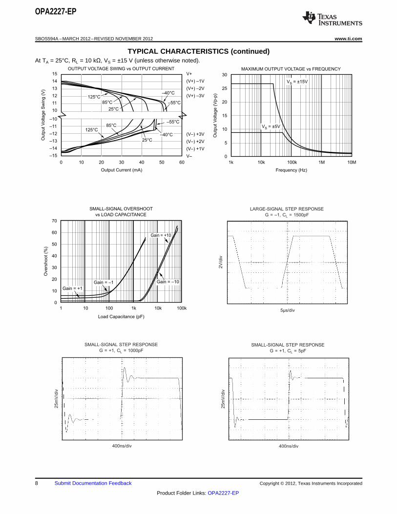
TYPICAL CHARACTERISTICS (continued)At TA = 25°C, RL = 10 kΩ, VS = ±15 V (unless otherwise noted).
8 Submit Documentation Feedback Copyright © 2012, Texas Instruments Incorporated
Product Folder Links: OPA2227-EP
OPA2227 Output
RF
500Ω
Input
–
+
OPA2227-EP
www.ti.com SBOS594A –MARCH 2012–REVISED NOVEMBER 2012
APPLICATION INFORMATION
Basic Connection
The OPA2227 is a precision operational amplifier with very low noise. It is unity-gain stable with a slew rate of2.3 V/μs and 8-MHz bandwidth. Applications with noisy or high impedance power supplies may requiredecoupling capacitors close to the device pins. In most cases, 0.1-μF capacitors are adequate.
Offset Voltage and Drift
The OPA2227 has very low offset voltage and drift. To achieve highest dc precision, circuit layout andmechanical conditions should be optimized. Connections of dissimilar metals can generate thermal potentials atthe op amp inputs which can degrade the offset voltage and drift. These thermocouple effects can exceed theinherent drift of the amplifier and ultimately degrade its performance. The thermal potentials can be made tocancel by assuring that they are equal at both input terminals. In addition:• Keep thermal mass of the connections made to the two input terminals similar.• Locate heat sources as far as possible from the critical input circuitry.• Shield operational amplifier and input circuitry from air currents such as those created by cooling fans.
Operating Voltage
OPA2227 operational amplifier operates from ±2.5-V to ±18-V supplies with excellent performance. Unlike mostoperational amplifiers which are specified at only one supply voltage, the OPA2227 is specified for real-worldapplications; a single set of specifications applies over the ±5-V to ±15-V supply range. Specifications areassured for applications between ±5-V and ±15-V power supplies. Some applications do not require equalpositive and negative output voltage swing. Power supply voltages do not need to be equal. The OPA2227 canoperate with as little as 5 V between the supplies and with up to 36 V between the supplies. For example, thepositive supply could be set to 25 V with the negative supply at –5 V or vice-versa. In addition, key parametersare assured over the specified temperature range, –55°C to 125°C. Parameters which vary significantly withoperating voltage or temperature are shown in the Typical Performance Curves.
Offset Voltage Adjustment
The OPA2227 is laser-trimmed for very low offset and drift so most applications will not require externaladjustment.
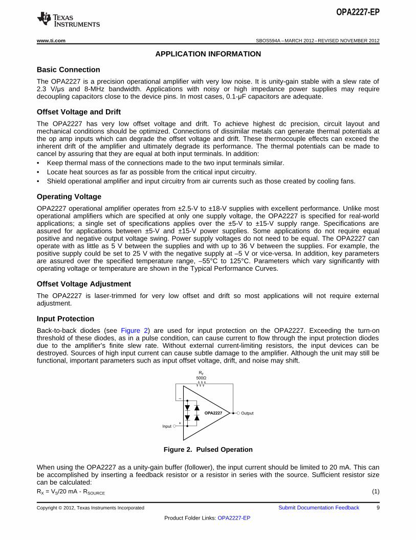
Input Protection
Back-to-back diodes (see Figure 2) are used for input protection on the OPA2227. Exceeding the turn-onthreshold of these diodes, as in a pulse condition, can cause current to flow through the input protection diodesdue to the amplifier’s finite slew rate. Without external current-limiting resistors, the input devices can bedestroyed. Sources of high input current can cause subtle damage to the amplifier. Although the unit may still befunctional, important parameters such as input offset voltage, drift, and noise may shift.
Figure 2. Pulsed Operation
When using the OPA2227 as a unity-gain buffer (follower), the input current should be limited to 20 mA. This canbe accomplished by inserting a feedback resistor or a resistor in series with the source. Sufficient resistor sizecan be calculated:RX = VS/20 mA - RSOURCE (1)
Copyright © 2012, Texas Instruments Incorporated Submit Documentation Feedback 9
Product Folder Links: OPA2227-EP
VOLTAGE NOISE SPECTRAL DENSITY
vs SOURCE RESISTANCE
100k 1M
Source Resistance, RS (Ω)
100 1k 10k
1.00+03
1.00E+02
1.00E+01
1.00E+00
Vo
tla
ge
No
ise
Sp
ectr
al D
en
sity,
E0
Typ
ica
l a
t 1
k (
V/
Hz)
√
OPA2227
Resistor Noise
Resistor Noise
OPA2227
RS
EO
EO2 = en
2 + (in RS)2 + 4kTRS
Op Amp
R1
R2
RB = R2 || R1 External Cancellation Resistor
Conventional Op Amp Configuration
OPA2227-EP
SBOS594A –MARCH 2012–REVISED NOVEMBER 2012 www.ti.com
where RX is either in series with the source or inserted in the feedback path. For example, for a 10-V pulse(VS = 10 V), total loop resistance must be 500 Ω. If the source impedance is large enough to sufficiently limit thecurrent on its own, no additional resistors are needed. The size of any external resistors must be carefullychosen since they will increase noise. See the Noise Performance section of this data sheet for furtherinformation on noise calculation. Figure 2 shows an example implementing a current limiting feedback resistor.
Input Bias Current Cancellation
The input bias current of the OPA2227 is internally compensated with an equal and opposite cancellation current.The resulting input bias current is the difference between with input bias current and the cancellation current. Theresidual input bias current can be positive or negative.
When the bias current is cancelled in this manner, the input bias current and input offset current areapproximately equal. A resistor added to cancel the effect of the input bias current (as shown in Figure 3) mayactually increase offset and noise and is therefore not recommended.
Figure 3. Input Bias Current Cancellation
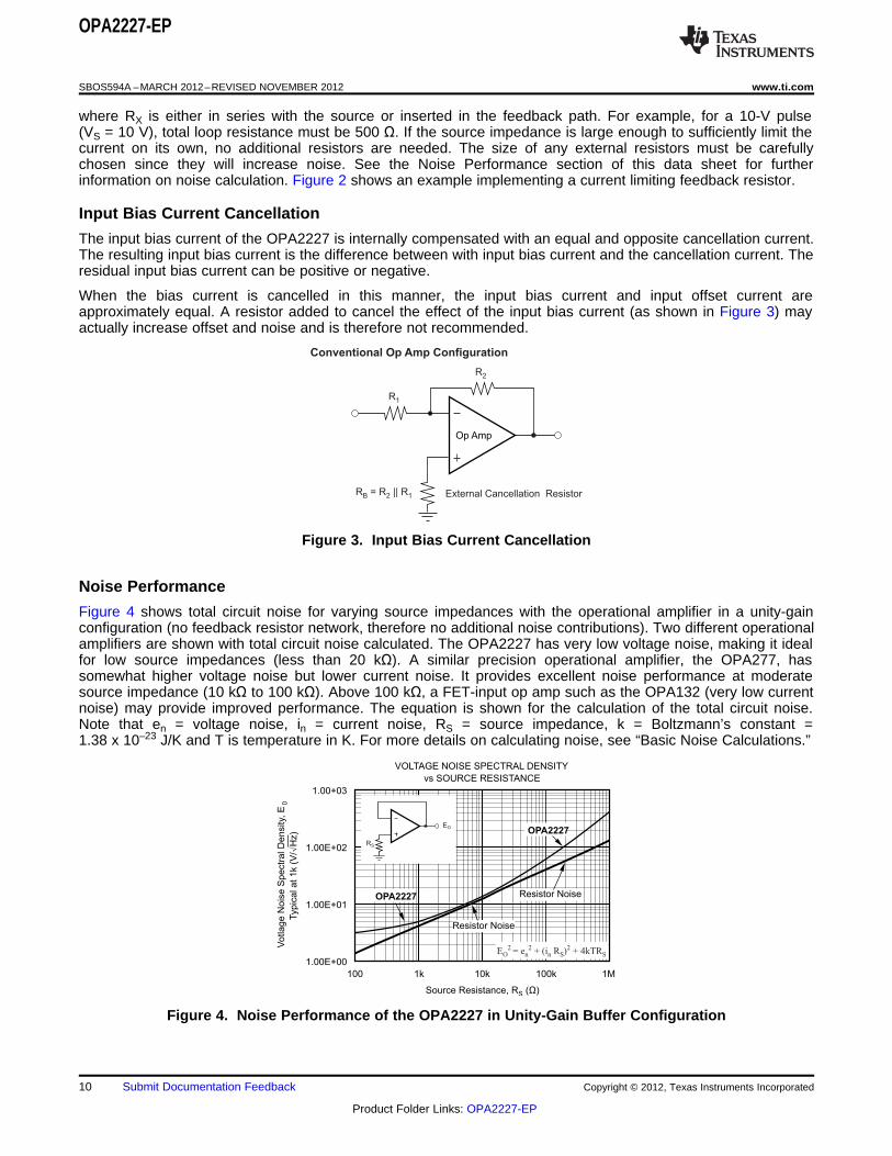
Noise Performance
Figure 4 shows total circuit noise for varying source impedances with the operational amplifier in a unity-gainconfiguration (no feedback resistor network, therefore no additional noise contributions). Two different operationalamplifiers are shown with total circuit noise calculated. The OPA2227 has very low voltage noise, making it idealfor low source impedances (less than 20 kΩ). A similar precision operational amplifier, the OPA277, hassomewhat higher voltage noise but lower current noise. It provides excellent noise performance at moderatesource impedance (10 kΩ to 100 kΩ). Above 100 kΩ, a FET-input op amp such as the OPA132 (very low currentnoise) may provide improved performance. The equation is shown for the calculation of the total circuit noise.Note that en = voltage noise, in = current noise, RS = source impedance, k = Boltzmann’s constant =1.38 x 10⁻²³ J/K and T is temperature in K. For more details on calculating noise, see “Basic Noise Calculations.”
Figure 4. Noise Performance of the OPA2227 in Unity-Gain Buffer Configuration
10 Submit Documentation Feedback Copyright © 2012, Texas Instruments Incorporated
Product Folder Links: OPA2227-EP
OPA2227-EP
www.ti.com SBOS594A –MARCH 2012–REVISED NOVEMBER 2012
Basic Noise Calculations
Design of low noise operational amplifier circuits requires careful consideration of a variety of possible noisecontributors: noise from the signal source, noise generated in the operational amplifier, and noise from thefeedback network resistors. The total noise of the circuit is the root-sum-square combination of all noisecomponents.
The resistive portion of the source impedance produces thermal noise proportional to the square root of theresistance. This function is shown plotted in Figure 4. Since the source impedance is usually fixed, select theoperational amplifier and the feedback resistors to minimize their contribution to the total noise.
Figure 4 shows total noise for varying source impedances with the operational amplifier in a unity-gainconfiguration (no feedback resistor network and therefore no additional noise contributions). The operationalamplifier itself contributes both a voltage noise component and a current noise component. The voltage noise iscommonly modeled as a time-varying component of the offset voltage. The current noise is modeled as the time-varying component of the input bias current and reacts with the source resistance to create a voltage componentof noise. Consequently, the lowest noise operational amplifier for a given application depends on the sourceimpedance. For low source impedance, current noise is negligible and voltage noise generally dominates. Forhigh source impedance, current noise may dominate.
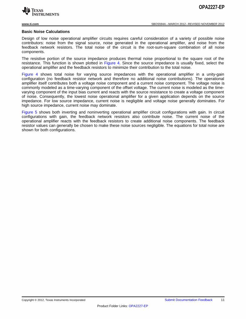
Figure 5 shows both inverting and noninverting operational amplifier circuit configurations with gain. In circuitconfigurations with gain, the feedback network resistors also contribute noise. The current noise of theoperational amplifier reacts with the feedback resistors to create additional noise components. The feedbackresistor values can generally be chosen to make these noise sources negligible. The equations for total noise areshown for both configurations.
Copyright © 2012, Texas Instruments Incorporated Submit Documentation Feedback 11
Product Folder Links: OPA2227-EP
R1
R2
EO
R1
R2
EORS
VS
RS
VS
Noise in Noninverting Gain Configuration
Noise in Inverting Gain Configuration
For op amps at 1kHz, en = 3nV/√Hz and in = 0.4pA/√Hz.
OPA2227-EP
SBOS594A –MARCH 2012–REVISED NOVEMBER 2012 www.ti.com
Figure 5. Noise Calculation in Gain Configurations
12 Submit Documentation Feedback Copyright © 2012, Texas Instruments Incorporated
Product Folder Links: OPA2227-EP
100kΩ
VOUT
1
2
3OPA2227
22pF
10Ω
Device
Under
Test
R4
9.09kΩ
R3
1kΩ
R7
97.6kΩ
R6
40.2kΩ
C2
1µF
C1
1µF C3
0.47µF
C4
22nF
R2
2MΩR8
402kΩ
R5
634kΩ
Input from
Device
Under
Test
R1
2MΩ
(OPA2227)
U1
(OPA2227)
U21
2
3
R10
226kΩ
R9
178kΩ
C5
0.47µF
C6
10nF
R11
178kΩ
(OPA2227)
U27
VOUT
6
5
OPA2227-EP
www.ti.com SBOS594A –MARCH 2012–REVISED NOVEMBER 2012
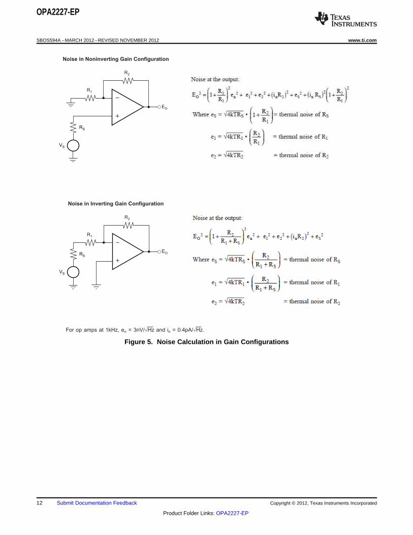
Figure 6 shows the 0.1-Hz to 10-Hz bandpass filter used to test the noise of the OPA2227. The filter circuit wasdesigned using Texas Instruments’ FilterPro software (available at www.ti.com). Figure 7 shows the configurationof the OPA2227 for noise testing.
Figure 6. 0.1-Hz to 10-Hz Bandpass Filter Used to Test Wideband Noise of the OPA2227
Figure 7. Noise Test Circuit
Copyright © 2012, Texas Instruments Incorporated Submit Documentation Feedback 13
Product Folder Links: OPA2227-EP
Output
NOTE: Use metal film resistors
and plastic film capacitor. Circuit
must be well shielded to achieve
low noise.
Responsivity 2.5 x 10≈4V/W
Output Noise 30µVrms, 0.1Hz to 10Hz≈
Dexter 1M
Thermopile
Detector
100Ω 100kΩ
OPA2227
2
3
1
0.1µF
VOUT
VIN
OPA2227
68nF
10nF
33nF
330pF
2.2nF
OPA2227
1.43kΩ 1.91kΩ
2.21kΩ
1.43kΩ
1.1kΩ
1.65kΩ1.1kΩ
fN = 13.86kHz
Q = 1.186
fN = 20.33kHz f = 7.2kHz
Q = 4.519
dc Gain = 1
2
1 6
3 7
5
OPA2227-EP
SBOS594A –MARCH 2012–REVISED NOVEMBER 2012 www.ti.com
Figure 8. Three-Pole, 20-kHz Low Pass, 0.5-dB Chebyshev Filter
Figure 9. Long-Wavelength Infrared Detector Amplifier
14 Submit Documentation Feedback Copyright © 2012, Texas Instruments Incorporated
Product Folder Links: OPA2227-EP
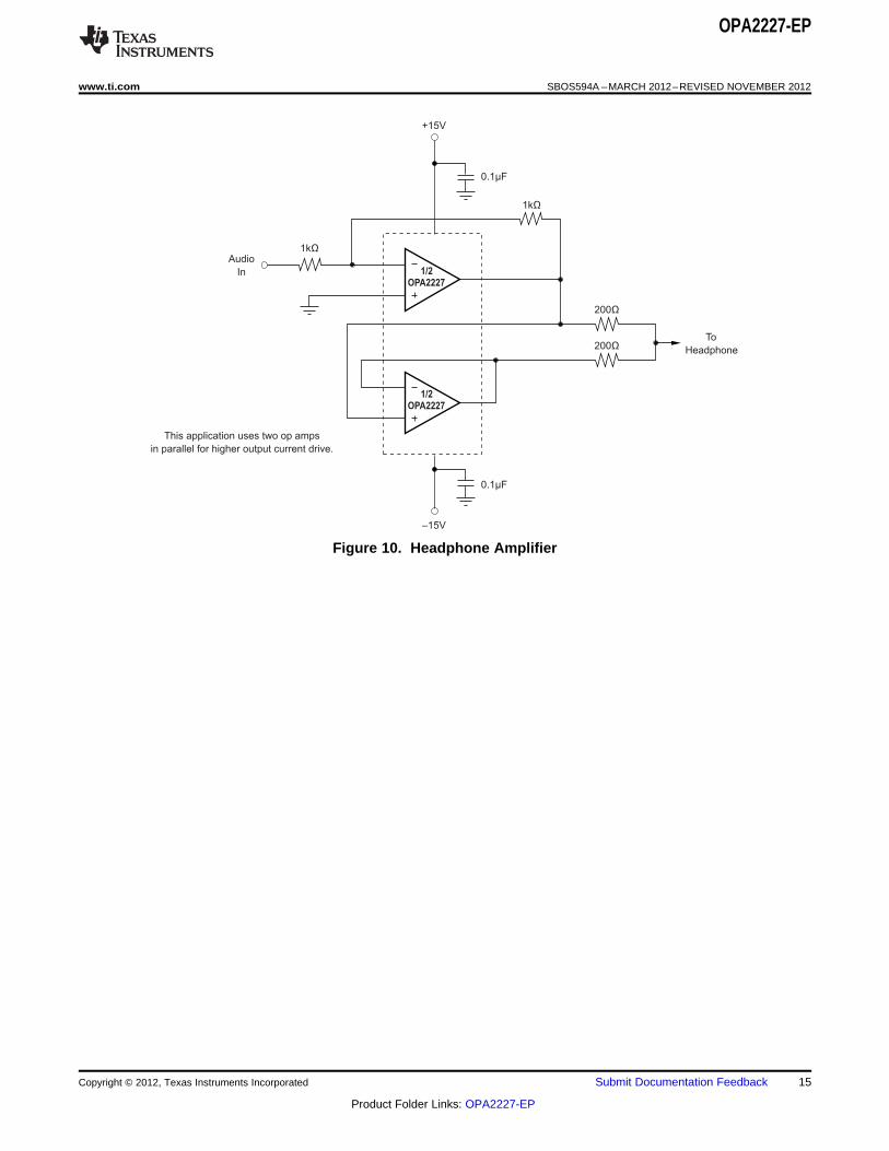
200Ω
200Ω
1kΩ
1kΩ
1/2OPA2227
1/2OPA2227
–15V
0.1µF
0.1µF
+15V
Audio
In
This application uses two op amps
in parallel for higher output current drive.
To
Headphone
OPA2227-EP
www.ti.com SBOS594A –MARCH 2012–REVISED NOVEMBER 2012
Figure 10. Headphone Amplifier
Copyright © 2012, Texas Instruments Incorporated Submit Documentation Feedback 15
Product Folder Links: OPA2227-EP
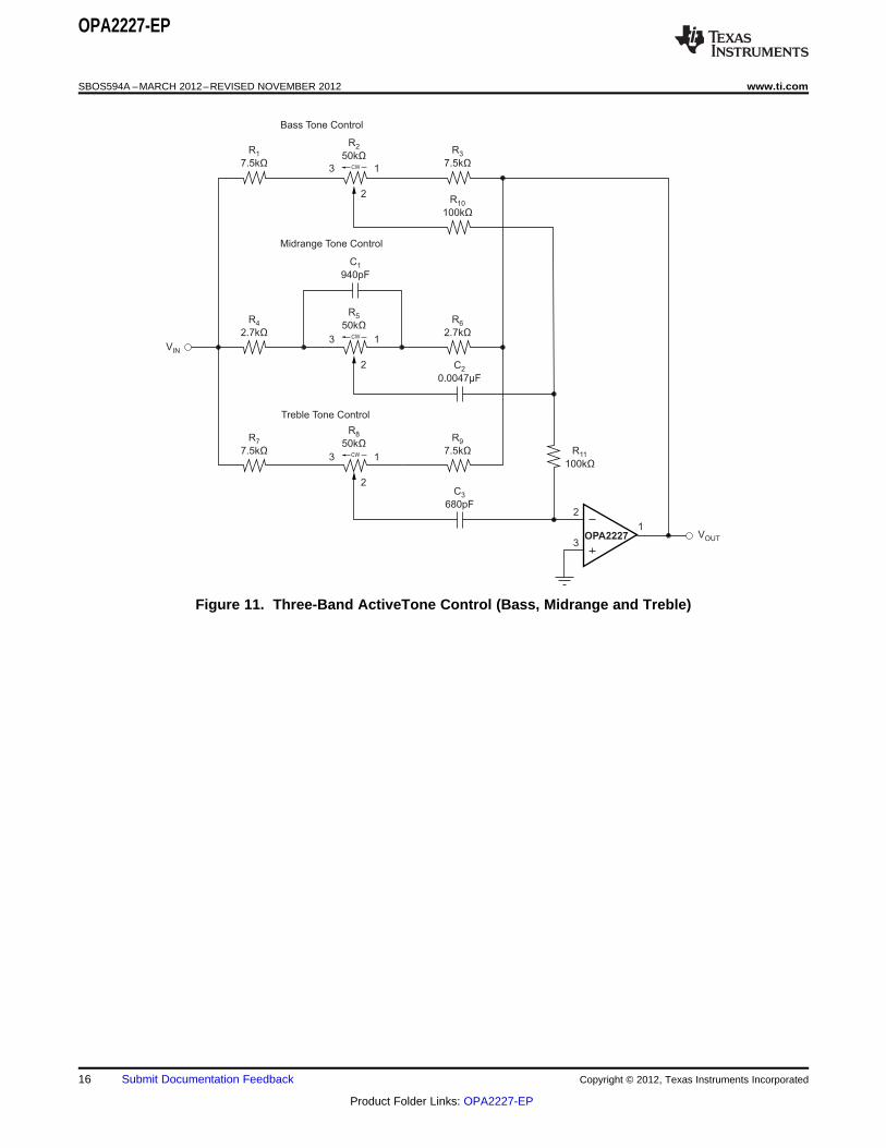
R5
50kΩR4
2.7kΩ
VIN
VOUT
R6
2.7kΩ
C1
940pF
C2
0.0047µF
C3
680pF
CW
CW
R2
50kΩR1
7.5kΩ
R3
7.5kΩ
R10
100kΩ
R8
50kΩR7
7.5kΩ
R9
7.5kΩ R11
100kΩCW
Bass Tone Control
Midrange Tone Control
Treble Tone Control
13
1
2
3
2
13
2
13
2
OPA2227
OPA2227-EP
SBOS594A –MARCH 2012–REVISED NOVEMBER 2012 www.ti.com
Figure 11. Three-Band ActiveTone Control (Bass, Midrange and Treble)
16 Submit Documentation Feedback Copyright © 2012, Texas Instruments Incorporated
Product Folder Links: OPA2227-EP
PACKAGE OPTION ADDENDUM
www.ti.com 24-Jan-2013
Addendum-Page 1
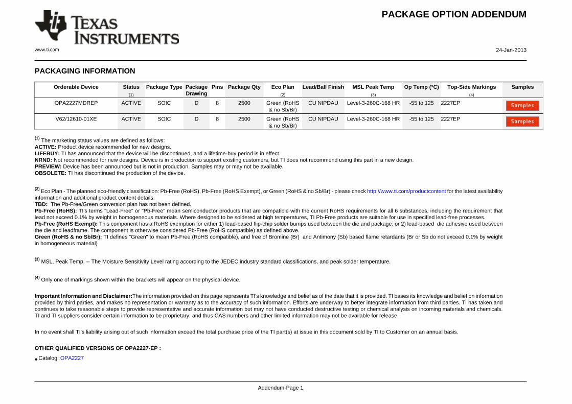
PACKAGING INFORMATION
Orderable Device Status(1)
Package Type PackageDrawing
Pins Package Qty Eco Plan(2)
Lead/Ball Finish MSL Peak Temp(3)
Op Temp (°C) Top-Side Markings(4)
Samples
OPA2227MDREP ACTIVE SOIC D 8 2500 Green (RoHS& no Sb/Br)
CU NIPDAU Level-3-260C-168 HR -55 to 125 2227EP
V62/12610-01XE ACTIVE SOIC D 8 2500 Green (RoHS& no Sb/Br)
CU NIPDAU Level-3-260C-168 HR -55 to 125 2227EP
(1) The marketing status values are defined as follows:ACTIVE: Product device recommended for new designs.LIFEBUY: TI has announced that the device will be discontinued, and a lifetime-buy period is in effect.NRND: Not recommended for new designs. Device is in production to support existing customers, but TI does not recommend using this part in a new design.PREVIEW: Device has been announced but is not in production. Samples may or may not be available.OBSOLETE: TI has discontinued the production of the device.
(2) Eco Plan - The planned eco-friendly classification: Pb-Free (RoHS), Pb-Free (RoHS Exempt), or Green (RoHS & no Sb/Br) - please check http://www.ti.com/productcontent for the latest availabilityinformation and additional product content details.TBD: The Pb-Free/Green conversion plan has not been defined.Pb-Free (RoHS): TI's terms "Lead-Free" or "Pb-Free" mean semiconductor products that are compatible with the current RoHS requirements for all 6 substances, including the requirement thatlead not exceed 0.1% by weight in homogeneous materials. Where designed to be soldered at high temperatures, TI Pb-Free products are suitable for use in specified lead-free processes.Pb-Free (RoHS Exempt): This component has a RoHS exemption for either 1) lead-based flip-chip solder bumps used between the die and package, or 2) lead-based die adhesive used betweenthe die and leadframe. The component is otherwise considered Pb-Free (RoHS compatible) as defined above.Green (RoHS & no Sb/Br): TI defines "Green" to mean Pb-Free (RoHS compatible), and free of Bromine (Br) and Antimony (Sb) based flame retardants (Br or Sb do not exceed 0.1% by weightin homogeneous material)
(3) MSL, Peak Temp. -- The Moisture Sensitivity Level rating according to the JEDEC industry standard classifications, and peak solder temperature.
(4) Only one of markings shown within the brackets will appear on the physical device.
Important Information and Disclaimer:The information provided on this page represents TI's knowledge and belief as of the date that it is provided. TI bases its knowledge and belief on informationprovided by third parties, and makes no representation or warranty as to the accuracy of such information. Efforts are underway to better integrate information from third parties. TI has taken andcontinues to take reasonable steps to provide representative and accurate information but may not have conducted destructive testing or chemical analysis on incoming materials and chemicals.TI and TI suppliers consider certain information to be proprietary, and thus CAS numbers and other limited information may not be available for release.
In no event shall TI's liability arising out of such information exceed the total purchase price of the TI part(s) at issue in this document sold by TI to Customer on an annual basis.
OTHER QUALIFIED VERSIONS OF OPA2227-EP :
• Catalog: OPA2227
PACKAGE OPTION ADDENDUM
www.ti.com 24-Jan-2013
Addendum-Page 2
NOTE: Qualified Version Definitions:
• Catalog - TI's standard catalog product
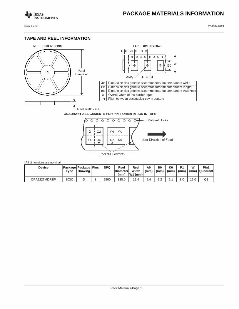
TAPE AND REEL INFORMATION
*All dimensions are nominal
Device PackageType
PackageDrawing
Pins SPQ ReelDiameter
(mm)
ReelWidth
W1 (mm)
A0(mm)
B0(mm)
K0(mm)
P1(mm)
W(mm)
Pin1Quadrant
OPA2227MDREP SOIC D 8 2500 330.0 12.4 6.4 5.2 2.1 8.0 12.0 Q1
PACKAGE MATERIALS INFORMATION
www.ti.com 25-Feb-2013
Pack Materials-Page 1
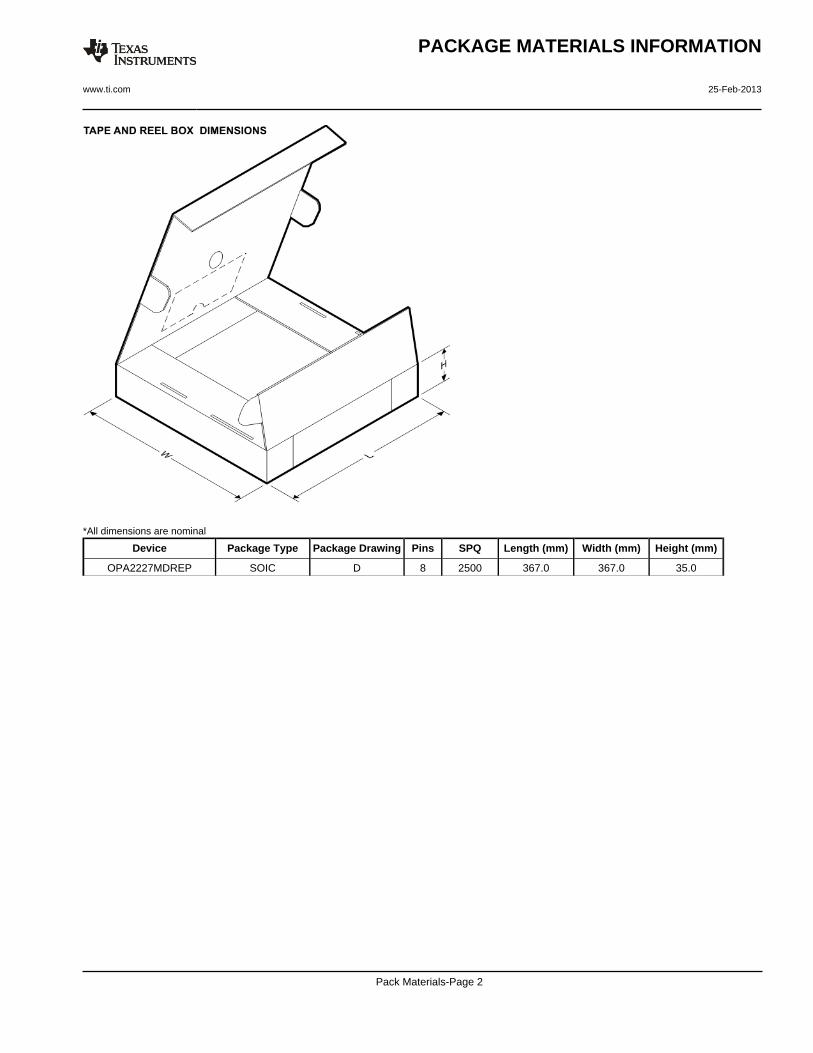
*All dimensions are nominal
Device Package Type Package Drawing Pins SPQ Length (mm) Width (mm) Height (mm)
OPA2227MDREP SOIC D 8 2500 367.0 367.0 35.0
PACKAGE MATERIALS INFORMATION
www.ti.com 25-Feb-2013
Pack Materials-Page 2
IMPORTANT NOTICE
Texas Instruments Incorporated and its subsidiaries (TI) reserve the right to make corrections, enhancements, improvements and otherchanges to its semiconductor products and services per JESD46, latest issue, and to discontinue any product or service per JESD48, latestissue. Buyers should obtain the latest relevant information before placing orders and should verify that such information is current andcomplete. All semiconductor products (also referred to herein as “components”) are sold subject to TI’s terms and conditions of salesupplied at the time of order acknowledgment.
TI warrants performance of its components to the specifications applicable at the time of sale, in accordance with the warranty in TI’s termsand conditions of sale of semiconductor products. Testing and other quality control techniques are used to the extent TI deems necessaryto support this warranty. Except where mandated by applicable law, testing of all parameters of each component is not necessarilyperformed.
TI assumes no liability for applications assistance or the design of Buyers’ products. Buyers are responsible for their products andapplications using TI components. To minimize the risks associated with Buyers’ products and applications, Buyers should provideadequate design and operating safeguards.
TI does not warrant or represent that any license, either express or implied, is granted under any patent right, copyright, mask work right, orother intellectual property right relating to any combination, machine, or process in which TI components or services are used. Informationpublished by TI regarding third-party products or services does not constitute a license to use such products or services or a warranty orendorsement thereof. Use of such information may require a license from a third party under the patents or other intellectual property of thethird party, or a license from TI under the patents or other intellectual property of TI.
Reproduction of significant portions of TI information in TI data books or data sheets is permissible only if reproduction is without alterationand is accompanied by all associated warranties, conditions, limitations, and notices. TI is not responsible or liable for such altereddocumentation. Information of third parties may be subject to additional restrictions.
Resale of TI components or services with statements different from or beyond the parameters stated by TI for that component or servicevoids all express and any implied warranties for the associated TI component or service and is an unfair and deceptive business practice.TI is not responsible or liable for any such statements.
Buyer acknowledges and agrees that it is solely responsible for compliance with all legal, regulatory and safety-related requirementsconcerning its products, and any use of TI components in its applications, notwithstanding any applications-related information or supportthat may be provided by TI. Buyer represents and agrees that it has all the necessary expertise to create and implement safeguards whichanticipate dangerous consequences of failures, monitor failures and their consequences, lessen the likelihood of failures that might causeharm and take appropriate remedial actions. Buyer will fully indemnify TI and its representatives against any damages arising out of the useof any TI components in safety-critical applications.
In some cases, TI components may be promoted specifically to facilitate safety-related applications. With such components, TI’s goal is tohelp enable customers to design and create their own end-product solutions that meet applicable functional safety standards andrequirements. Nonetheless, such components are subject to these terms.
No TI components are authorized for use in FDA Class III (or similar life-critical medical equipment) unless authorized officers of the partieshave executed a special agreement specifically governing such use.
Only those TI components which TI has specifically designated as military grade or “enhanced plastic” are designed and intended for use inmilitary/aerospace applications or environments. Buyer acknowledges and agrees that any military or aerospace use of TI componentswhich have not been so designated is solely at the Buyer's risk, and that Buyer is solely responsible for compliance with all legal andregulatory requirements in connection with such use.
TI has specifically designated certain components as meeting ISO/TS16949 requirements, mainly for automotive use. In any case of use ofnon-designated products, TI will not be responsible for any failure to meet ISO/TS16949.
Products Applications
Audio www.ti.com/audio Automotive and Transportation www.ti.com/automotive
Amplifiers amplifier.ti.com Communications and Telecom www.ti.com/communications
Data Converters dataconverter.ti.com Computers and Peripherals www.ti.com/computers
DLP® Products www.dlp.com Consumer Electronics www.ti.com/consumer-apps
DSP dsp.ti.com Energy and Lighting www.ti.com/energy
Clocks and Timers www.ti.com/clocks Industrial www.ti.com/industrial
Interface interface.ti.com Medical www.ti.com/medical
Logic logic.ti.com Security www.ti.com/security
Power Mgmt power.ti.com Space, Avionics and Defense www.ti.com/space-avionics-defense
Microcontrollers microcontroller.ti.com Video and Imaging www.ti.com/video
RFID www.ti-rfid.com
OMAP Applications Processors www.ti.com/omap TI E2E Community e2e.ti.com
Wireless Connectivity www.ti.com/wirelessconnectivity
Mailing Address: Texas Instruments, Post Office Box 655303, Dallas, Texas 75265Copyright © 2013, Texas Instruments Incorporated