
Heterogeneous material integration for...
100
Heterogeneous material integration for MEMS FREDRIK FORSBERG Doctoral Thesis Stockholm, Sweden 2013
Transcript of Heterogeneous material integration for...
Heterogeneous material integration for MEMS
FREDRIK FORSBERG
Doctoral ThesisStockholm, Sweden 2013
Front cover pictures:The front cover shows an array of 17 μm pitch microbolometers and an array of460 × 460 μm2 silicon dies.
TRITA-EE 2013:039ISSN 1653-5146ISBN 978-91-7501-891-1
KTH Royal Institute of TechnologySchool of Electrical Engineering
Micro and Nanosystems
Akademisk avhandling som med tillstand av Kungliga Tekniska hogskolan framlaggestill offentlig granskning for avlaggande av teknologie doktorsexamen i elektriskmätteknik fredagen den 25 oktober 2013 klockan 10.00 i Kollegiesalen, Brinellvägen8, KTH, Stockholm.
Thesis for the degree of Doctor of Philosophy at KTH Royal Institute of Technology,Stockholm, Sweden.
© Fredrik Forsberg, September 2013
Tryck: Universitetsservice US AB, Stockholm, 2013
iii
Abstract
This thesis describes heterogeneous integration methods for the fabrica-tion of microelectromechanical systems (MEMS). Most MEMS devices reusethe fabrication techniques that are found in the microelectronics integratedcircuit industry. This limits the selection of materials and processes thatare feasible for the realization of MEMS devices. Heterogeneous integrationmethods, on the other hand, consist of the separate pre-fabrication ofsub-components followed by an assembly step. The pre-fabrication ofsubcomponents opens up for a wider selection of fabrication technologiesand thus potentially better performing and more optimized devices. Thefirst part of the thesis is focused upon an adhesive wafer-level layer transfermethod to fabricate resistive microbolometer-based long-wavelength infraredfocal plane arrays. This is realized by a CMOS-compatible transfer ofmonocrystalline silicon with epitaxially grown silicon-germanium quantumwells. Heterogeneous transfer methods are also used for the realization offiltering devices, integration of distributed small dies onto larger wafer formatsand to fabricate a graphene-based pressure sensor. The filtering devicesconsist of very fragile nano-porous membranes that with the presented dryadhesive methods can be transferred without clogging or breaking. Pick-and-place methods for the massive transfer of small dies between differentwafer formats are limited by time and die size-considerations. Our presentedsolution solves these problems by expanding a die array on a flexible tape,followed by adhesive wafer bonding to a target wafer. Furthermore, a gaugepressure sensor is realized by transferring a graphene monolayer grown ona copper foil to a micromachined target wafer with a silicon oxide interfacelayer. This device is used to extract the gauge factor of graphene. Adhesivebonding is an enabling technology for the presented heterogeneous integrationtechniques. A blister test method together with an experimental setup tocharacterize the bond energies between adhesives and bonded substrates isalso presented.
Fredrik ForsbergNano and Microsystems, KTH School of electrical engineeringKTH Royal Institute of Technology, SE-100 44 Stockholm, Sweden

Contents
Contents vList of papers . . . . . . . . . . . . . . . . . . . . . . . . . . . . . . . . . . vii
1 Introduction 11.1 Monolithic integration of MEMS and ICs . . . . . . . . . . . . . . . 21.2 Heterogeneous integration of MEMS and ICs . . . . . . . . . . . . . 71.3 Comparison of monolithic and heterogeneous integration approaches 101.4 Outline of the thesis . . . . . . . . . . . . . . . . . . . . . . . . . . . 10
2 Uncooled microbolometer-based focal plane arrays 132.1 Introduction . . . . . . . . . . . . . . . . . . . . . . . . . . . . . . . . 132.2 Optimization parameters for resistive microbolometers . . . . . . . . 162.3 Monolithically integrated LWIR FPAs . . . . . . . . . . . . . . . . . 182.4 Heterogeneous integration of LWIR FPAs . . . . . . . . . . . . . . . 212.5 Discussion . . . . . . . . . . . . . . . . . . . . . . . . . . . . . . . . . 31
3 Evaluation of bond energy in adhesive wafer bonding 333.1 Introduction . . . . . . . . . . . . . . . . . . . . . . . . . . . . . . . . 333.2 Methods for evaluating bond energy . . . . . . . . . . . . . . . . . . 343.3 Blister test evaluation platform . . . . . . . . . . . . . . . . . . . . . 353.4 Tabulated bond energies . . . . . . . . . . . . . . . . . . . . . . . . . 363.5 Discussion . . . . . . . . . . . . . . . . . . . . . . . . . . . . . . . . . 36
4 Heterogeneous integration of nanoporous membranes 394.1 Introduction . . . . . . . . . . . . . . . . . . . . . . . . . . . . . . . . 394.2 OSTE+ enabled transfer bonding of porous membranes . . . . . . . 404.3 Filter characterization . . . . . . . . . . . . . . . . . . . . . . . . . . 424.4 Discussion . . . . . . . . . . . . . . . . . . . . . . . . . . . . . . . . . 44
5 Heterogeneous transfer of distributed die arrays 475.1 Introduction . . . . . . . . . . . . . . . . . . . . . . . . . . . . . . . . 475.2 Self-assembly methods . . . . . . . . . . . . . . . . . . . . . . . . . . 485.3 Parallel transfer methods . . . . . . . . . . . . . . . . . . . . . . . . 49
v
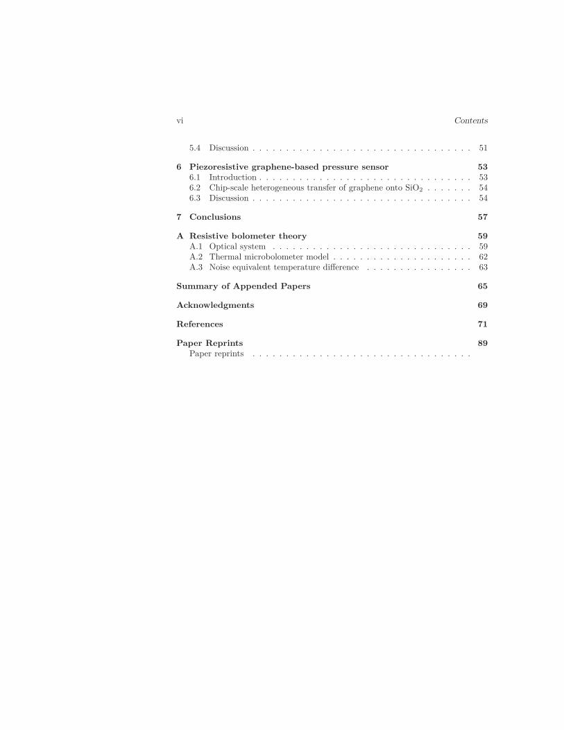
vi Contents
5.4 Discussion . . . . . . . . . . . . . . . . . . . . . . . . . . . . . . . . . 51
6 Piezoresistive graphene-based pressure sensor 536.1 Introduction . . . . . . . . . . . . . . . . . . . . . . . . . . . . . . . . 536.2 Chip-scale heterogeneous transfer of graphene onto SiO2 . . . . . . . 546.3 Discussion . . . . . . . . . . . . . . . . . . . . . . . . . . . . . . . . . 54
7 Conclusions 57
A Resistive bolometer theory 59A.1 Optical system . . . . . . . . . . . . . . . . . . . . . . . . . . . . . . 59A.2 Thermal microbolometer model . . . . . . . . . . . . . . . . . . . . . 62A.3 Noise equivalent temperature difference . . . . . . . . . . . . . . . . 63
Summary of Appended Papers 65
Acknowledgments 69
References 71
Paper Reprints 89Paper reprints . . . . . . . . . . . . . . . . . . . . . . . . . . . . . . . . .
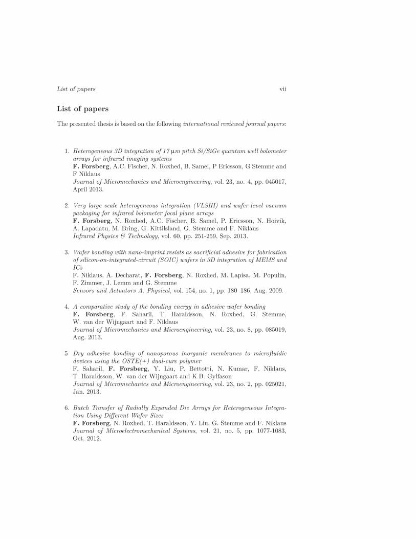
List of papers vii
List of papers
The presented thesis is based on the following international reviewed journal papers:
1. Heterogeneous 3D integration of 17 μm pitch Si/SiGe quantum well bolometerarrays for infrared imaging systemsF. Forsberg, A.C. Fischer, N. Roxhed, B. Samel, P Ericsson, G Stemme andF NiklausJournal of Micromechanics and Microengineering, vol. 23, no. 4, pp. 045017,April 2013.
2. Very large scale heterogeneous integration (VLSHI) and wafer-level vacuumpackaging for infrared bolometer focal plane arraysF. Forsberg, N. Roxhed, A.C. Fischer, B. Samel, P. Ericsson, N. Hoivik,A. Lapadatu, M. Bring, G. Kittilsland, G. Stemme and F. NiklausInfrared Physics & Technology, vol. 60, pp. 251-259, Sep. 2013.
3. Wafer bonding with nano-imprint resists as sacrificial adhesive for fabricationof silicon-on-integrated-circuit (SOIC) wafers in 3D integration of MEMS andICsF. Niklaus, A. Decharat, F. Forsberg, N. Roxhed, M. Lapisa, M. Populin,F. Zimmer, J. Lemm and G. StemmeSensors and Actuators A: Physical, vol. 154, no. 1, pp. 180–186, Aug. 2009.
4. A comparative study of the bonding energy in adhesive wafer bondingF. Forsberg, F. Saharil, T. Haraldsson, N. Roxhed, G. Stemme,W. van der Wijngaart and F. NiklausJournal of Micromechanics and Microengineering, vol. 23, no. 8, pp. 085019,Aug. 2013.
5. Dry adhesive bonding of nanoporous inorganic membranes to microfluidicdevices using the OSTE(+) dual-cure polymerF. Saharil, F. Forsberg, Y. Liu, P. Bettotti, N. Kumar, F. Niklaus,T. Haraldsson, W. van der Wijngaart and K.B. GylfasonJournal of Micromechanics and Microengineering, vol. 23, no. 2, pp. 025021,Jan. 2013.
6. Batch Transfer of Radially Expanded Die Arrays for Heterogeneous Integra-tion Using Different Wafer SizesF. Forsberg, N. Roxhed, T. Haraldsson, Y. Liu, G. Stemme and F. NiklausJournal of Microelectromechanical Systems, vol. 21, no. 5, pp. 1077-1083,Oct. 2012.
viii Contents
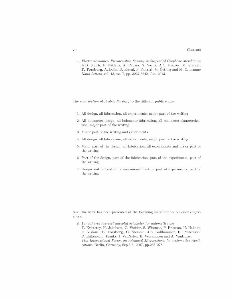
7. Electromechanical Piezoresistive Sensing in Suspended Graphene MembranesA.D. Smith, F. Niklaus, A. Paussa, S. Vaziri, A.C. Fischer, M. Sterner,F. Forsberg, A. Delin, D. Esseni, P. Palestri, M. Ostling and M. C. LemmeNano Letters, vol. 13, no. 7, pp. 3237-3242, Jun. 2013.
The contribution of Fredrik Forsberg to the different publications:
1. All design, all fabrication, all experiments, major part of the writing
2. All bolometer design, all bolometer fabrication, all bolometer characteriza-tion, major part of the writing
3. Minor part of the writing and experiments
4. All design, all fabrication, all experiments, major part of the writing
5. Major part of the design, all fabrication, all experiments and major part ofthe writing
6. Part of the design, part of the fabrication, part of the experiments, part ofthe writing
7. Design and fabrication of measurement setup, part of experiments, part ofthe writing
Also, the work has been presented at the following international reviewed confer-ences:
8. Far infrared low-cost uncooled bolometer for automotive useT. Kvisteroy, H. Jakobsen, C. Vieider, S. Wissmar, P. Ericsson, U. Halldin,F. Niklaus, F. Forsberg, G. Stemme, J.E. Kallhammer, H. Pettersson,D. Eriksson, J. Franks, J. VanNylen, H. Vercammen and A. VanHulsel11th International Forum on Advanced Microsystems for Automotive Appli-cations, Berlin, Germany, Sep.5-6, 2007, pp.265–278
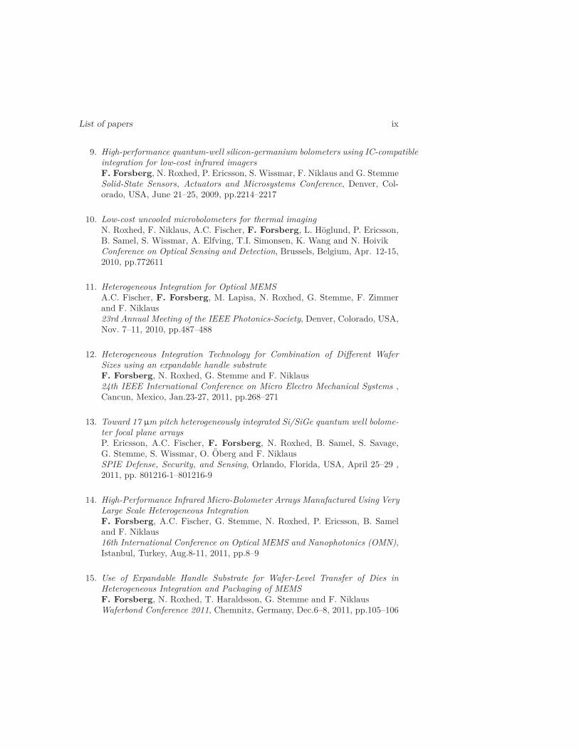
List of papers ix
9. High-performance quantum-well silicon-germanium bolometers using IC-compatibleintegration for low-cost infrared imagersF. Forsberg, N. Roxhed, P. Ericsson, S. Wissmar, F. Niklaus and G. StemmeSolid-State Sensors, Actuators and Microsystems Conference, Denver, Col-orado, USA, June 21–25, 2009, pp.2214–2217
10. Low-cost uncooled microbolometers for thermal imagingN. Roxhed, F. Niklaus, A.C. Fischer, F. Forsberg, L. Hoglund, P. Ericsson,B. Samel, S. Wissmar, A. Elfving, T.I. Simonsen, K. Wang and N. HoivikConference on Optical Sensing and Detection, Brussels, Belgium, Apr. 12-15,2010, pp.772611
11. Heterogeneous Integration for Optical MEMSA.C. Fischer, F. Forsberg, M. Lapisa, N. Roxhed, G. Stemme, F. Zimmerand F. Niklaus23rd Annual Meeting of the IEEE Photonics-Society, Denver, Colorado, USA,Nov. 7–11, 2010, pp.487–488
12. Heterogeneous Integration Technology for Combination of Different WaferSizes using an expandable handle substrateF. Forsberg, N. Roxhed, G. Stemme and F. Niklaus24th IEEE International Conference on Micro Electro Mechanical Systems ,Cancun, Mexico, Jan.23-27, 2011, pp.268–271
13. Toward 17 μm pitch heterogeneously integrated Si/SiGe quantum well bolome-ter focal plane arraysP. Ericsson, A.C. Fischer, F. Forsberg, N. Roxhed, B. Samel, S. Savage,G. Stemme, S. Wissmar, O. Oberg and F. NiklausSPIE Defense, Security, and Sensing, Orlando, Florida, USA, April 25–29 ,2011, pp. 801216-1–801216-9
14. High-Performance Infrared Micro-Bolometer Arrays Manufactured Using VeryLarge Scale Heterogeneous IntegrationF. Forsberg, A.C. Fischer, G. Stemme, N. Roxhed, P. Ericsson, B. Sameland F. Niklaus16th International Conference on Optical MEMS and Nanophotonics (OMN),Istanbul, Turkey, Aug.8-11, 2011, pp.8–9
15. Use of Expandable Handle Substrate for Wafer-Level Transfer of Dies inHeterogeneous Integration and Packaging of MEMSF. Forsberg, N. Roxhed, T. Haraldsson, G. Stemme and F. NiklausWaferbond Conference 2011, Chemnitz, Germany, Dec.6–8, 2011, pp.105–106
x Contents
16. Wafer-level heterogeneous 3D integration for MEMS and NEMSF. Niklaus, M. Lapisa, S. Bleiker, V. Dubois, N. Roxhed, A.C. Fischer,F. Forsberg, G. Stemme, D. Grogg and M. Despont3rd IEEE International Workshop on Low Temperature Bonding for 3DIntegration, Tokyo, Japan, May 22–23, 2012, pp.247–252
17. High-Resolution Micropatterning of Off-Stoichiometric Thiol-enes (OSTE)Via a Novel Lithography MechanismJ.M. Karlsson,F. Carlborg, F. Saharil, F. Forsberg, F. Niklaus,W. van der Wijngaart and T. HaraldssonThe 16th International Conference on Miniaturized Systems for Chemistryand Life Sciences, Okinawa, Japan, Oct28-Nov.1, 2012, pp.225–227
18. Low temperature adhesive wafer bonding using OSTE(+) for heterogeneous3D MEMS integrationF. Forsberg, F. Saharil, G. Stemme, N. Roxhed, W. van der Wijngaart,T. Haraldsson and F. NiklausIEEE 26th International Conference on Micro Electro Mechanical Systems,Taipei, Taiwan, Jan.20-24, 2013, pp.342–346

Nomenclature
α-Si Amorphous silicon
AlGe Aluminum-Germanium
BCB Benzocyclobutene
CMP Chemical-mechanical polishing
Cu Copper
D∗ Specific detectivity
DRIE Deep reactive ion etching
FPA Focal plane array
IC Integrated circuit
LWIR Long wavelength infrared
MEMS Microelectromechanical systems
NEMS Nanoelectromechanical systems
NEP Noise-equivalent power
NETD Noise-equivalent temperature difference
Ni Nickel
PECVD Plasma-enhanced chemical vapor deposition
poly-Si Polycrystalline silicon
PSD Power spectral density
QW Quantum-well
SEM Scanning electron microscopy
xi
xii Contents
Si Silicon
SiGe Silicon-Germanium
SiN Silicon nitride
SiOx Silicon oxide
SiP System in package
Sn Tin
SNR Signal-to-noise ratio
SoB System on board
SoC System on board
SOI Silicon on insulator
TCR Temperature coefficent of resistance
TiW Titanium Tungsten
VOx Vanadium oxide
Chapter 1
Introduction
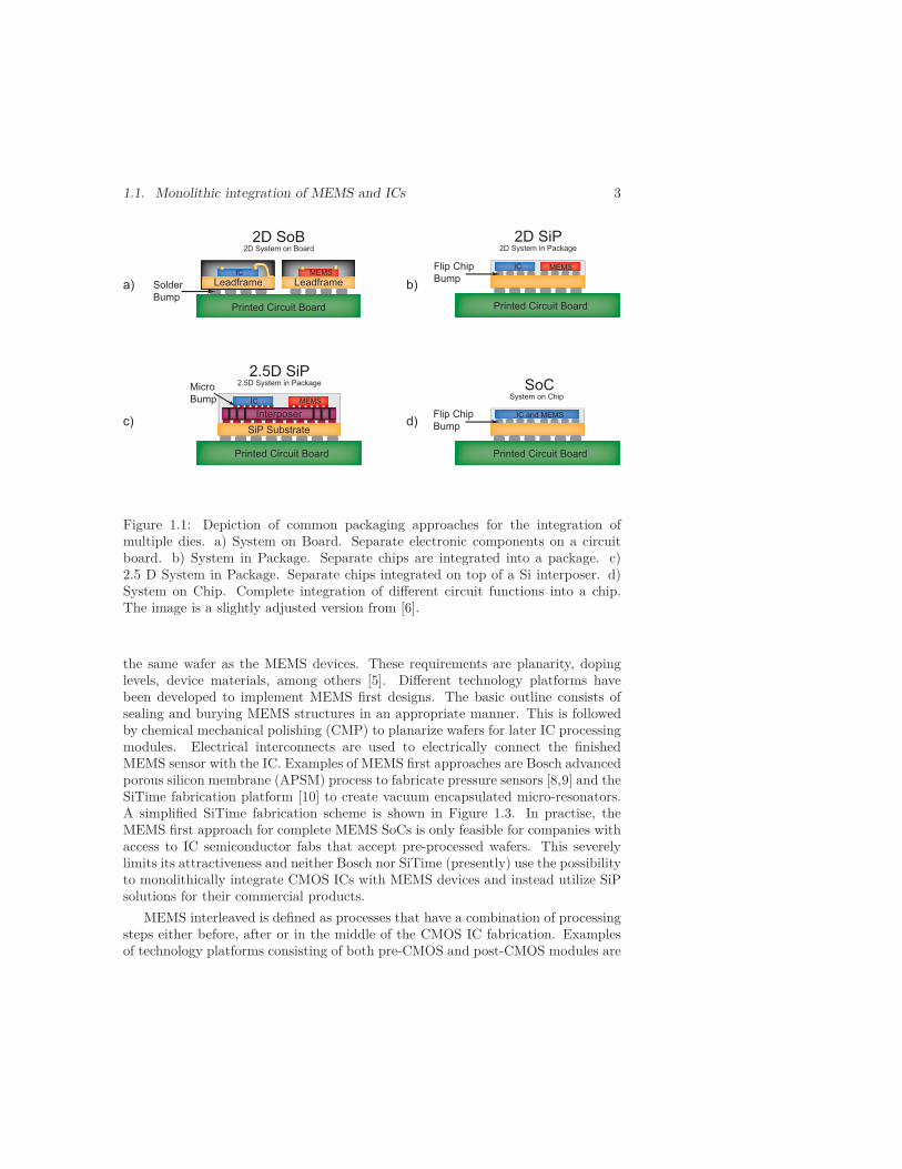
The last two decades have seen an enormous increase in both the volume andthe technological refinement of transducers and sensor systems. The underlyingfactor in this trend has been the development of microelectromechanical systems(MEMS), which are used to perform the essential new technological feats thathave become part of our everyday experience. A modern smart phone, forexample, contains accelerometers, gyroscopes, barometric sensors, microphones andoscillators that more often than not are constructed with MEMS microfabricationmethods [1, 2]. Other areas where MEMS-based devices proliferate is in inkjetprintheads, digital light processors and filters. Most MEMS-based sensors andtransducers need to be combined with intelligence in the form of integrated circuits(IC) to be useful. The functionalities that are implemented include analog-to-digital conversion, amplification, filtering, information processing and as thecommunication interface between the MEMS component and the rest of the system.The increased integration of functionality in sensor systems has evolved the typicalsystem layout from separate components on a printed circuit board (SoB), tointegration of the system components (i.e IC and MEMS) into a package (SiP)and to complete integration of a system onto a single microchip (SoC). Figure 1.1schematically exemplifies the technological development pattern. The technologicalfrontier is pushed forward towards higher levels of integration by the need of smallerform factors, signal speed, lower cost and energy efficiency among others.
The most relevant fabrication methods for the realization of MEMS devicesutilize the knowledge and tools that have been developed for the last fifty yearsfor the fabrication of integrated electronic circuits. The strong influence frommicroelectronics is visible in both the use of materials and the fabrication cycle.Typically, silicon (Si) substrates are used as the base material. The fabricationcycle that follows consists of modifying the surface of the Si substrate. That canbe achieved by, for example, doping the Si substrate, surface oxidation of Si ordeposition of material on top of the Si substrate. The next step consists of selectiveremoval of unwanted material in patterned areas of the substrate. This is done
1
2 Chapter 1. Introduction
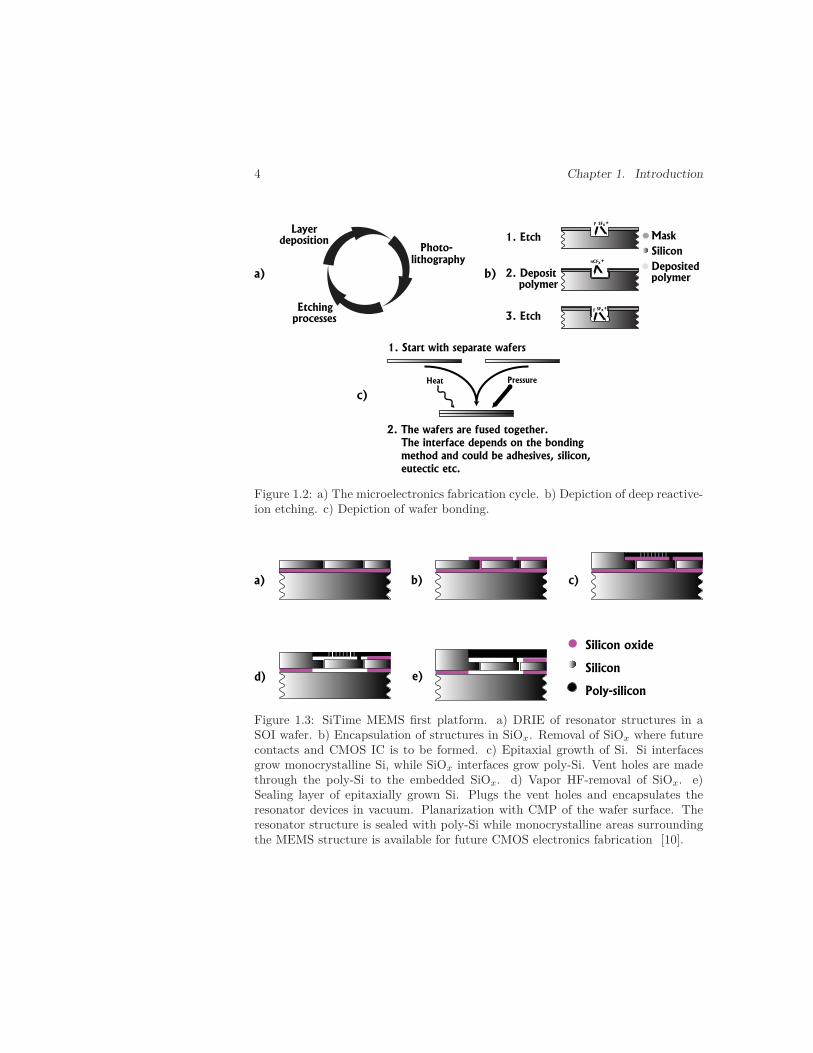
by covering the substrate with a photo-sensitive polymer. The photo-sensitivepolymer is then photolithographically patterned into the surface structure we wantto imprint. The last step consist of a selective removal of unwanted material byetching in the areas not covered by the photo-sensitive polymer. The results of thecycle is a Si substrate with a patterned layer on top. By repeating the deposition-patterning-etching cycle, different material layers and patterns can be formed ontop of the Si substrate, which in turn form the wanted devices. There are importantdifferences in the fabrication of MEMS devices and microelectronic devices. Thefabrication of ICs is essentially a planar 2D-process where only a very thin surfacelayer of the Si substrate is needed by the transistors that the ICs are based upon.Presently, typical gate lengths of the transistors used in modern digital ICs are 28nanometers and below [3]. In comparison MEMS devices are huge. From μm-sizedto mm-sized devices. Furthermore, MEMS devices are typically 3D-structures withconsiderably thicker material layers than what is used in microelectronics. Thisintroduces the need for specialized MEMS fabrication methods. Technologies ofconsiderable importance in MEMS fabrication is deep reactive-ion etching (DRIE)and wafer bonding, which in turn enables the etching of deep structures in Si and theattachment of different substrates to each other. These two fabrication technologiesleverage the methods taken from microelectronics to enable the formation of true3D-devices. Figure 1.2 summarizes the fabrication cycle. The interested reader isreferred to dedicated texts for in depth descriptions of established microfabricationmethods [4, 5].
Two different approaches are utilized in the fabrication of MEMS SoCs, wherethe sensor is integrated together with the IC on the same chip. The firstmethod is based on monolithic integration. This approach follows closely thedeposition-patterning-etch cycle described above where the needed material layersare deposited on top of the wafer substrate, followed by etching. The secondmethod, which is the focus of this thesis, instead consists of the separate fabricationof sub-components of the system that in an integration step is attached to each otherto form the finished devices. This approach is called heterogeneous integration.
1.1 Monolithic integration of MEMS and ICs
There are three ways in which ICs and MEMS can be monolithically integrated intoSoCs [7]. The first method consists of processing the MEMS first and the ICs last,typically next to the sensor. The second method interleaves the fabrication of boththe MEMS devices and the ICs by processing steps that are used in both fabricationschemes. The last method starts with fabricating the ICs first and the MEMS last,typically on top of the ICs in deposited material layers. All three platforms havebeen used commercially in the realization of microsystems.
Monolithic integration based on MEMS first processes allows for a very highthermal budget in the fabrication of the MEMS devices. Strict requirements areintroduced to the MEMS fabrication since the later fabrication of ICs are made on
1.1. Monolithic integration of MEMS and ICs 3
a) b)
c) d)
2.5D SiP2.5D System in Package
Printed Circuit Board
IC MEMS
SiP Substrate
Interposer
Micro
Bump
2D SoB2D System on Board
Printed Circuit Board
Solder
Bump
IC MEMS
Leadframe Leadframe
SoCSystem on Chip
Printed Circuit Board
IC and MEMSFlip Chip
Bump
2D SiP2D System in Package
Printed Circuit Board
ICFlip Chip
Bump
MEMS
Figure 1.1: Depiction of common packaging approaches for the integration ofmultiple dies. a) System on Board. Separate electronic components on a circuitboard. b) System in Package. Separate chips are integrated into a package. c)2.5 D System in Package. Separate chips integrated on top of a Si interposer. d)System on Chip. Complete integration of different circuit functions into a chip.The image is a slightly adjusted version from [6].
the same wafer as the MEMS devices. These requirements are planarity, dopinglevels, device materials, among others [5]. Different technology platforms havebeen developed to implement MEMS first designs. The basic outline consists ofsealing and burying MEMS structures in an appropriate manner. This is followedby chemical mechanical polishing (CMP) to planarize wafers for later IC processingmodules. Electrical interconnects are used to electrically connect the finishedMEMS sensor with the IC. Examples of MEMS first approaches are Bosch advancedporous silicon membrane (APSM) process to fabricate pressure sensors [8,9] and theSiTime fabrication platform [10] to create vacuum encapsulated micro-resonators.A simplified SiTime fabrication scheme is shown in Figure 1.3. In practise, theMEMS first approach for complete MEMS SoCs is only feasible for companies withaccess to IC semiconductor fabs that accept pre-processed wafers. This severelylimits its attractiveness and neither Bosch nor SiTime (presently) use the possibilityto monolithically integrate CMOS ICs with MEMS devices and instead utilize SiPsolutions for their commercial products.
MEMS interleaved is defined as processes that have a combination of processingsteps either before, after or in the middle of the CMOS IC fabrication. Examplesof technology platforms consisting of both pre-CMOS and post-CMOS modules are
4 Chapter 1. Introduction
Photo-lithography
Etching processes
Layer deposition
F SFx+
F SFx+
nCFx+
1. Etch
3. Etch
2. Deposit polymer
Silicon
Mask
Depositedpolymer
1. Start with separate wafers
Heat Pressure
a)
c)
b)
2. The wafers are fused together.
The interface depends on the bonding
method and could be adhesives, silicon,
eutectic etc.
Figure 1.2: a) The microelectronics fabrication cycle. b) Depiction of deep reactive-ion etching. c) Depiction of wafer bonding.
a)
Silicon
Silicon oxide
Poly-silicon
b) c)
e)d)
Figure 1.3: SiTime MEMS first platform. a) DRIE of resonator structures in aSOI wafer. b) Encapsulation of structures in SiOx. Removal of SiOx where futurecontacts and CMOS IC is to be formed. c) Epitaxial growth of Si. Si interfacesgrow monocrystalline Si, while SiOx interfaces grow poly-Si. Vent holes are madethrough the poly-Si to the embedded SiOx. d) Vapor HF-removal of SiOx. e)Sealing layer of epitaxially grown Si. Plugs the vent holes and encapsulates theresonator devices in vacuum. Planarization with CMP of the wafer surface. Theresonator structure is sealed with poly-Si while monocrystalline areas surroundingthe MEMS structure is available for future CMOS electronics fabrication [10].
1.1. Monolithic integration of MEMS and ICs 5
a)
Silicon
Silicon oxide
Poly-silicon
g)f)
e)d)
c)b)
Silicon-nitride
Metal
interconnects
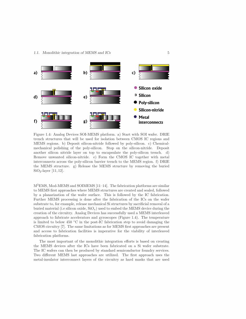
Figure 1.4: Analog Devices SOI-MEMS platform. a) Start with SOI wafer. DRIEtrench structures that will be used for isolation between CMOS IC regions andMEMS regions. b) Deposit silicon-nitride followed by poly-silicon. c) Chemical-mechanical polishing of the poly-silicon. Stop on the silicon-nitride. Depositanother silicon nitride layer on top to encapsulate the poly-silicon trench. d)Remove unwanted silicon-nitride. e) Form the CMOS IC together with metalinterconnects across the poly-silicon barrier trench to the MEMS region. f) DRIEthe MEMS structure. g) Release the MEMS structure by removing the buriedSiO2-layer [11,12].
M3EMS, Mod-MEMS and SOIMEMS [11–14]. The fabrication platforms are similarto MEMS first approaches where MEMS structures are created and sealed, followedby a planarization of the wafer surface. This is followed by the IC fabrication.Further MEMS processing is done after the fabrication of the ICs on the wafersubstrate to, for example, release mechanical Si structures by sacrificial removal of aburied material (i.e silicon oxide, SiOx) used to embed the MEMS device during thecreation of the circuitry. Analog Devices has successfully used a MEMS interleavedapproach to fabricate accelerators and gyroscopes (Figure 1.4). The temperatureis limited to below 450 ◦C in the post-IC fabrication step to avoid damaging theCMOS circuitry [7]. The same limitations as for MEMS first approaches are presentand access to fabrication facilities is imperative for the viability of interleavedfabrication platforms.
The most important of the monolithic integration efforts is based on creatingthe MEMS devices after the ICs have been fabricated on a Si wafer substrate.The IC wafers can then be produced by standard semiconductor foundry services.Two different MEMS last approaches are utilized. The first approach uses themetal-insulator interconnect layers of the circuitry as hard masks that are used
6 Chapter 1. Introduction
SiliconDielectric
Polymer Metal
a)
d)
c)
b)
IC region
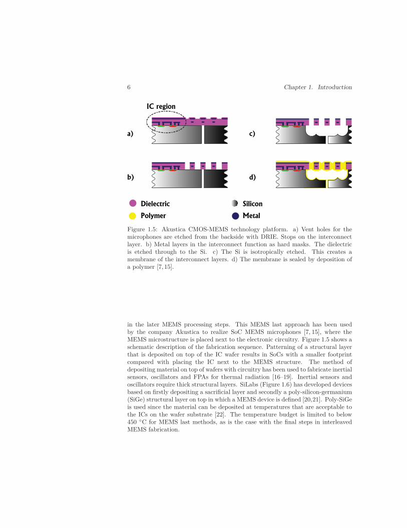
Figure 1.5: Akustica CMOS-MEMS technology platform. a) Vent holes for themicrophones are etched from the backside with DRIE. Stops on the interconnectlayer. b) Metal layers in the interconnect function as hard masks. The dielectricis etched through to the Si. c) The Si is isotropically etched. This creates amembrane of the interconnect layers. d) The membrane is sealed by deposition ofa polymer [7, 15].
in the later MEMS processing steps. This MEMS last approach has been usedby the company Akustica to realize SoC MEMS microphones [7, 15], where theMEMS microstructure is placed next to the electronic circuitry. Figure 1.5 shows aschematic description of the fabrication sequence. Patterning of a structural layerthat is deposited on top of the IC wafer results in SoCs with a smaller footprintcompared with placing the IC next to the MEMS structure. The method ofdepositing material on top of wafers with circuitry has been used to fabricate inertialsensors, oscillators and FPAs for thermal radiation [16–19]. Inertial sensors andoscillators require thick structural layers. SiLabs (Figure 1.6) has developed devicesbased on firstly depositing a sacrificial layer and secondly a poly-silicon-germanium(SiGe) structural layer on top in which a MEMS device is defined [20,21]. Poly-SiGeis used since the material can be deposited at temperatures that are acceptable tothe ICs on the wafer substrate [22]. The temperature budget is limited to below450 ◦C for MEMS last methods, as is the case with the final steps in interleavedMEMS fabrication.
1.2. Heterogeneous integration of MEMS and ICs 7
Silicon
Dielectric Hard mask
Metal
a)
f)e)d)
c)b)
Poly Si-Ge
Germanium
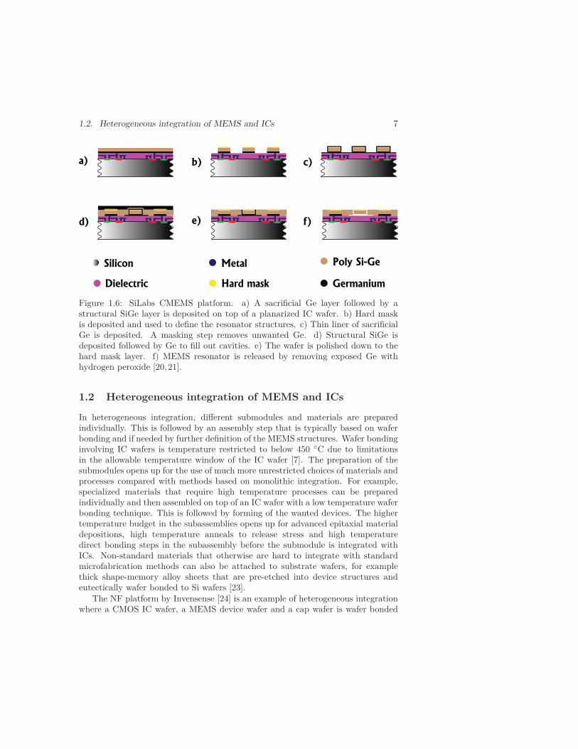
Figure 1.6: SiLabs CMEMS platform. a) A sacrificial Ge layer followed by astructural SiGe layer is deposited on top of a planarized IC wafer. b) Hard maskis deposited and used to define the resonator structures. c) Thin liner of sacrificialGe is deposited. A masking step removes unwanted Ge. d) Structural SiGe isdeposited followed by Ge to fill out cavities. e) The wafer is polished down to thehard mask layer. f) MEMS resonator is released by removing exposed Ge withhydrogen peroxide [20, 21].
1.2 Heterogeneous integration of MEMS and ICs
In heterogeneous integration, different submodules and materials are preparedindividually. This is followed by an assembly step that is typically based on waferbonding and if needed by further definition of the MEMS structures. Wafer bondinginvolving IC wafers is temperature restricted to below 450 ◦C due to limitationsin the allowable temperature window of the IC wafer [7]. The preparation of thesubmodules opens up for the use of much more unrestricted choices of materials andprocesses compared with methods based on monolithic integration. For example,specialized materials that require high temperature processes can be preparedindividually and then assembled on top of an IC wafer with a low temperature waferbonding technique. This is followed by forming of the wanted devices. The highertemperature budget in the subassemblies opens up for advanced epitaxial materialdepositions, high temperature anneals to release stress and high temperaturedirect bonding steps in the subassembly before the submodule is integrated withICs. Non-standard materials that otherwise are hard to integrate with standardmicrofabrication methods can also be attached to substrate wafers, for examplethick shape-memory alloy sheets that are pre-etched into device structures andeutectically wafer bonded to Si wafers [23].
The NF platform by Invensense [24] is an example of heterogeneous integrationwhere a CMOS IC wafer, a MEMS device wafer and a cap wafer is wafer bonded
8 Chapter 1. Introduction
Silicon
Silicon oxide Germanium
Aluminum
a) b)
d) e)
c)
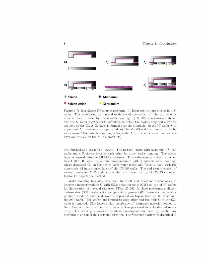
Figure 1.7: InvenSense NF-shuttle platform. a) Deep cavities are etched in a Siwafer. This is followed by thermal oxidation of the wafer. b) The cap wafer isattached to a Si wafer by fusion wafer bonding. c) MEMS structures are etchedinto the Si wafer together with standoffs to define the sealing ring and electricalcontacts to the IC. A Ge-layer is formed over the standoffs. d) An IC wafer withuppermost Al interconnects is prepared. e) The MEMS wafer is bonded to the ICwafer using AlGe eutectic bonding between the Al in the uppermost interconnectlayer and the Ge on the MEMS wafer [24].
into finished and assembled devices. The method starts with fastening a Si capwafer and a Si device layer to each other by direct wafer bonding. The devicelayer is formed into the MEMS structures. This subassembly is then attachedto a CMOS IC wafer by aluminium-germanium (AlGe) eutectic wafer bonding,where deposited Ge on the device layer wafer reacts and forms a bond with theuppermost Al interconnect layer of the CMOS wafer. The end results consist ofvacuum packaged MEMS structures that are placed on top of CMOS circuitry.Figure 1.7 depicts the method.
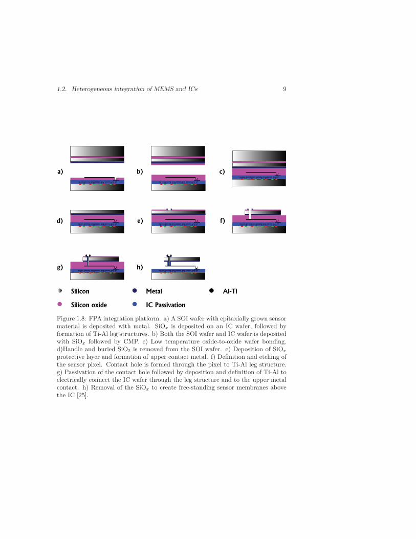
Wafer bonding has also been used by KTH and Sensonor Technologies tointegrate monocrystalline Si with SiGe quantum-wells (QW) on top of IC wafersfor the creation of thermal radiation FPAs [25, 26]. In these platforms, a silicon-on-insulator (SOI) wafer with an epitaxially grown QW thermistor material ispre-fabricated. A sacrificial layer is deposited on top of both an IC wafer andthe SOI wafer. The wafers are bonded to each other and the bulk Si of the SOIwafer is removed. This leaves a thin membrane of thermistor material bonded tothe IC wafer. The thin thermistor layer is then processed into the desired sensorarrays. The last step removes the sacrificial bonding material, leaving free-standingmembranes on top of the electronic circuitry. The Sensonor platform is described in
1.2. Heterogeneous integration of MEMS and ICs 9
Silicon
Silicon oxide IC Passivation
Metal
a) b)
d) e)
c)
f)
g) h)
Al-Ti
Figure 1.8: FPA integration platform. a) A SOI wafer with epitaxially grown sensormaterial is deposited with metal. SiOx is deposited on an IC wafer, followed byformation of Ti-Al leg structures. b) Both the SOI wafer and IC wafer is depositedwith SiOx followed by CMP. c) Low temperature oxide-to-oxide wafer bonding.d)Handle and buried SiO2 is removed from the SOI wafer. e) Deposition of SiOx
protective layer and formation of upper contact metal. f) Definition and etching ofthe sensor pixel. Contact hole is formed through the pixel to Ti-Al leg structure.g) Passivation of the contact hole followed by deposition and definition of Ti-Al toelectrically connect the IC wafer through the leg structure and to the upper metalcontact. h) Removal of the SiOx to create free-standing sensor membranes abovethe IC [25].
10 Chapter 1. Introduction
Figure 1.8 while the KTH platform is presented in chapter 2. A similar integrationplatform has also been used for the creation of micro-mirrors on top of CMOSelectronics [27,28].
1.3 Comparison of monolithic and heterogeneousintegration approaches
One recurring problem of MEMS fabrication can be summarized in the expression’one product, one process, one package’. This captures the specialized natureof different MEMS sensors that typically require different and product-specificfabrication approaches. This presents multiple problems regarding yield, time-to-market and ease of manufacture since each and every product need to beoptimized individually. An ideal and flexible fabrication platform that can bereused for different MEMS devices should allow: a wide selection of materials,a large temperature window, limited investments in fabrication equipments andthe use of fabless manufacturing services.
Monolithic MEMS first and MEMS interleaved integration with ICs requireownership of IC manufacturing lines or close cooperation with a semiconductorfoundry, due to the non-standard fabrication sequence compared with normal ICproduction. This limits its viability in practice. The development cost and yieldis also potentially problematic compared with standard IC fabrication. MEMSlast fabrication techniques opens up for the use of standard IC wafers fromsemiconductor foundries. This can be followed by MEMS processing steps thatpotentially can be outsourced to MEMS foundry services. Stress issues andlimited choices of acceptable MEMS materials are issues of concern since MEMSlast monolithic integration methods require a limited temperature budget below450 ◦C to avoid damaging the ICs. Heterogeneous integration methods potentiallyalleviate many of the concerns that are present with the other methods. Itallows for a more unrestricted fabrication of product-specific submodules that areintegrated using a standardized integration scheme. The heterogeneous integrationscheme preferably also include a standardized wafer-level packaging strategy. Thefabrication of different product specific submodules opens up for the reuse ofthe same heterogeneous integration platform for different devices. This savesdevelopment time and potentially increases the yield since all submodules (IC,MEMS, packaging cap wafer etc.) can be prepared with methods that are optimizedfor quality and manufacturability before the use of a standardized heterogeneousintegration method for the device assembly.
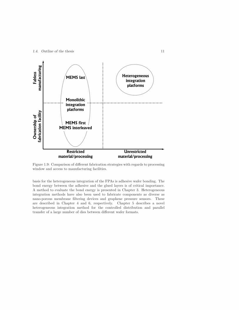
1.4 Outline of the thesis
Chapter 2 consists of an introduction to uncooled resistive microbolometersand describes a method based on heterogeneous integration to realize resistivemicrobolometer focal plane arrays (FPA) in a CMOS IC-compatible process. The
1.4. Outline of the thesis 11
Fab
less
man
ufa
cturing
Ow
ners
hip
of
fabrica
tion f
acility
Restricted
material/processing
Unrestricted
material/processing
MEMS first
MEMS interleaved
MEMS last Heterogeneous
integration
platforms
Monolithic
integration
platforms
Figure 1.9: Comparison of different fabrication strategies with regards to processingwindow and access to manufacturing facilities.
basis for the heterogeneous integration of the FPAs is adhesive wafer bonding. Thebond energy between the adhesive and the glued layers is of critical importance.A method to evaluate the bond energy is presented in Chapter 3. Heterogeneousintegration methods have also been used to fabricate components as diverse asnano-porous membrane filtering devices and graphene pressure sensors. Theseare described in Chapter 4 and 6, respectively. Chapter 5 describes a novelheterogeneous integration method for the controlled distribution and paralleltransfer of a large number of dies between different wafer formats.

Chapter 2
Uncooled microbolometer-basedfocal plane arrays
2.1 Introduction
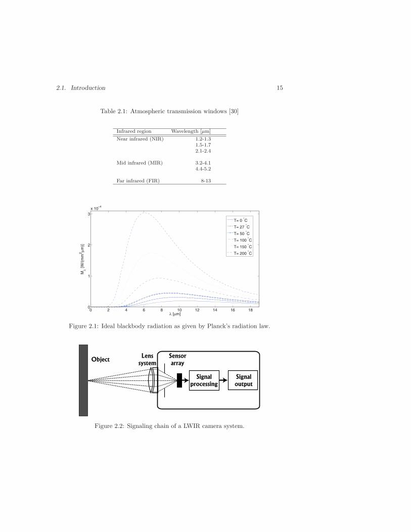
Blackbody radiation is emitted by all objects with a non-zero temperature. Theelectromagnetic spectrum and intensity of an ideal blackbody is given by Planck’sradiation law (Figure 2.1). In the real world, objects differ from the ideal blackbodyemission. The emissivity of a material is the relative ability of its surface to emitenergy by radiation compared with an ideal blackbody. Thus, the emissivity is1 for an ideal blackbody and down to below 0.1 for polished metal surfaces [29].The emitted electromagnetic radiation is radiated through the atmosphere, whereparts of the radiation is absorbed depending on its wavelength. This creates infraredatmospheric transmission windows (Table 2.1) with a low attenuation of the infraredradiation [30].
Long-wavelength infrared(LWIR) camera systems are designed to detect theblackbody radiation. The radiation is captured by LWIR optics and is focuseddown onto a sensor array (Figure 2.2). The spectrum of the blackbody radiationthat is emitted by objects in ambient temperature has a maximum intensityaround a wavelength of 10 μm, which is inside the far infrared (FIR) atmospherictransmission window. Thus, LWIR sensors are usually optimized to absorb thermalradiation between wavelengths of 8-14 μm to maximize the detector signal. Inprinciple, there are two ways to sense incoming infrared radiation. Either photonicsensors are used. These are typically based on photoconductors or photodiodeswhere incoming photons generate charge carriers. The main limitation of thismethod is that it requires substantial cooling below ambient temperature to reduceelectronic noise due to thermally excited current carriers. Thermal sensors, on theother hand, are sensors that absorb the incoming infrared radiation and experiencea change in their temperature. This temperature change is in turn convertedinto an electric output signal that can be probed. Thermal infrared sensors can,
13
14 Chapter 2. Uncooled microbolometer-based focal plane arrays
unlike photonic sensors, be operated uncooled at ambient temperature. Thischaracteristic makes uncooled thermal infrared sensors useful for small, lightweightand portable products [29]. A variety of different physical operating principlesare used to realize thermal infrared sensors, although the basic structure of thesensor is the same. A well-isolated detector element absorbs incident LWIRradiant flux and converts it into heat energy that increases the temperature ofthe detector element. The resulting temperature increase is related to the powerof the absorbed LWIR radiation and the responsivity is in theory wavelength-independent [30]. In reality, the design of the LWIR absorbing structure will createa wavelength dependent responsivity of the output signal due to differences inthe absorption of different wavelengths. The increase in temperature is sensedby either transducer-based detector elements or parametric sensors, where thetemperature of the sensor element modulates an electric signal. Examples ofLWIR transducers are pyroelectric sensors [31–33] and thermocouple/thermopilebased sensors that utilize the Seebeck effect [34, 35]. Parametric sensors are basedon a range of physical effects. Among these are the temperature-dependenceof the electrical resistance [36–46], temperature-dependence of the pressure inenclosed gas cavities (i.e Golay cells) [47], temperature-dependence of bimaterialmechanical structures [48, 49] and the temperature-dependence of diode forwardvoltage drops [50–54].
The commercially most successful of the physical principles to realize FPAsconsists of resistive microbolometers, which is also the focus of the Work discussedin this Chapter. The change in resistance due to the incident LWIR radiation ismeasured for each microbolometer in the FPA, which together registers the thermalimage information. Figure 2.3 depicts the outlay of a resistive microbolometer. Itconsists of a free-standing membrane of a thin material that experience a changein resistance with temperature. The membrane is connected to a readout ICthrough the leg structure. The leg structure functions both as a thermal pathbetween the membrane and the surroundings and as an electrical connection.A maximized output signal requires a minimized thermal conductance from themembrane. That is realized by vacuum encapsulation of the microbolometertogether with an optimized leg structure regarding its choice of materials and design.The microbolometer legs and membrane need to be stress compensated to avoida thermal short circuit between the microbolometer membrane and the bottomsubstrate. A high signal-to-noise ratio of the electrical output signal depends onthe temperature coefficient of resistance (TCR), electrical noise and the thermalinsulation of the sensor membrane [30,55, 56]. Furthermore, optical considerationsfor the membrane need to be taken in regard to optimize the absorbance ofincident LWIR radiation [57,58]. The next sections will delineate important designparameters to optimize in the realization of LWIR FPAs and show examples ofmonolithically integrated LWIR FPAs. This is followed by a description of howto realize heterogeneously integrated FPAs. A theoretical treatment of resistivemicrobolometer-based FPAs is presented in Appendix A.
2.1. Introduction 15
Table 2.1: Atmospheric transmission windows [30]
Infrared region Wavelength [μm]Near infrared (NIR) 1.2-1.3
1.5-1.72.1-2.4
Mid infrared (MIR) 3.2-4.14.4-5.2
Far infrared (FIR) 8-13
0 2 4 6 8 10 12 14 16 180
1
2
3x 10
−4
λ [μm]
Mλ [W
/(m
m2 μ
m)]
T= 0 °C
T= 27 °C
T= 50 °C
T= 100 °C
T= 150 °C
T= 200 °C
Figure 2.1: Ideal blackbody radiation as given by Planck’s radiation law.
ObjectLens
system
Sensor
array
Signal
processing
Signal
output
Figure 2.2: Signaling chain of a LWIR camera system.
16 Chapter 2. Uncooled microbolometer-based focal plane arrays
Plated Nickel pillar
Leg structure
Trench
Si/SiGeTop contact
Al mirror
Read-out wafer
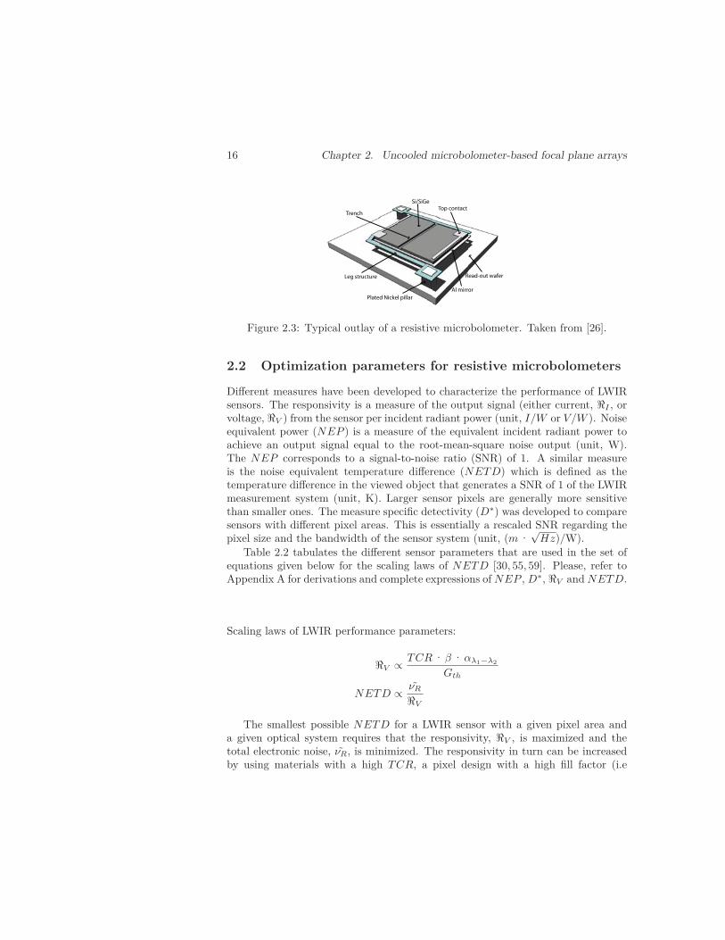
Figure 2.3: Typical outlay of a resistive microbolometer. Taken from [26].
2.2 Optimization parameters for resistive microbolometers
Different measures have been developed to characterize the performance of LWIRsensors. The responsivity is a measure of the output signal (either current, �I , orvoltage, �V ) from the sensor per incident radiant power (unit, I/W or V/W ). Noiseequivalent power (NEP ) is a measure of the equivalent incident radiant power toachieve an output signal equal to the root-mean-square noise output (unit, W).The NEP corresponds to a signal-to-noise ratio (SNR) of 1. A similar measureis the noise equivalent temperature difference (NETD) which is defined as thetemperature difference in the viewed object that generates a SNR of 1 of the LWIRmeasurement system (unit, K). Larger sensor pixels are generally more sensitivethan smaller ones. The measure specific detectivity (D∗) was developed to comparesensors with different pixel areas. This is essentially a rescaled SNR regarding thepixel size and the bandwidth of the sensor system (unit, (m ·
√Hz)/W).
Table 2.2 tabulates the different sensor parameters that are used in the set ofequations given below for the scaling laws of NETD [30, 55, 59]. Please, refer toAppendix A for derivations and complete expressions of NEP , D∗, �V and NETD.
Scaling laws of LWIR performance parameters:
�V ∝ TCR · β · αλ1−λ2
Gth
NETD ∝ νR
�V
The smallest possible NETD for a LWIR sensor with a given pixel area anda given optical system requires that the responsivity, �V , is maximized and thetotal electronic noise, νR, is minimized. The responsivity in turn can be increasedby using materials with a high TCR, a pixel design with a high fill factor (i.e
2.2. Optimization parameters for resistive microbolometers 17
Table 2.2: Microbolometer parameters
Parameter Unit Description
T CR %K
Temperaturecoefficient ofresistance.
β - Microbolometer fill fac-tor.
αλ1−λ2 - Relative infrared ab-sorbtion in the wave-length interval λ1 − λ2.
GthWK
Thermal conductance.νR V Total voltage noise.
the relative area used by the microbolometer absorption structure), high LWIRabsorption and a high thermal insulation.
A high thermal insulation is achieved by vacuum encapsulation of the FPAtogether with leg structures that are as long and thin as possible [60]. Long legscan be achieved by curling them up in meander structures. This increases the areaof the pixel that is used by the leg structures compared with the sensor membrane(thermistor) and decreases the pixel fill factor. One method to achieve a high fillfactor together with the use of long meander leg structures consists of building two-or three layer structures [37,54]. The bottom layer or layers consists of leg structuresthat fill the pixel area with curled meander-shaped legs. The top layer consists of anumbrella-shaped absorption structure that enables a high microbolometer fill factorand couples the absorbed heat into a thermistor. This kind of structures increasethe microbolometer performance with the cost of increased fabrication complexity.
Electronic noise consists of many different noise components that are weightedtogether. Contributions to the noise in uncooled thermal LWIR systems arisefrom the readout IC, the microbolometer sensor and thermal fluctuations inthe microbolometer [55, 59]. The readout IC generally contributes less noisecompared to the contribution from the microbolometer sensor [59]. Different noisecontributions in the microbolometer thermistor material have different spectralproperties and magnitudes. Examples of electronic noise in a microbolometer areJohnson-Nyquist noise, shot noise and flicker noise (1/f -noise) [61]. Of these, the1/f -noise of the microbolometer, in a well-designed system, dominates the totalnoise in the output signal [56, 59]. Minimization of the microbolometer noise andwith that the system noise is thus focused on the minimization of the flicker noise.The flicker noise can be quantified by the equation [62,63]:
SI
I2bias
=α
Nfγ
18 Chapter 2. Uncooled microbolometer-based focal plane arrays
λ/4
Mirror
Absorbing
sensor membrane λ/4n
Mirror
Absorbing
sensor membrane
a) b)
Figure 2.4: λ/4-wavelength absorption structure arrangements. a) Thin semi-transparent membrane vacuum-separated λ/4 from an LWIR mirror. b) λ/(4n)-thick semitransparent membrane with a directly attached LWIR mirror on thebackside of the membrane, where n is the refractive index of the membrane material.
where SI is the noise power, Ibias is the bias current, N is the total number offree charges in the thermistor material, α is known as Hooge’s constant and γ is aparameter close to 1. Minimization of the flicker noise is dependent on minimizingαN which is also known as the K-parameter for the thermistor material [64].Different electrically contacted thermistor materials have drastically different noiseproperties. The 1/f -noise depends on among others the quality of deposition,what thermistor material is used, the quality of electrical contacts and the sidewallpassivation [25].
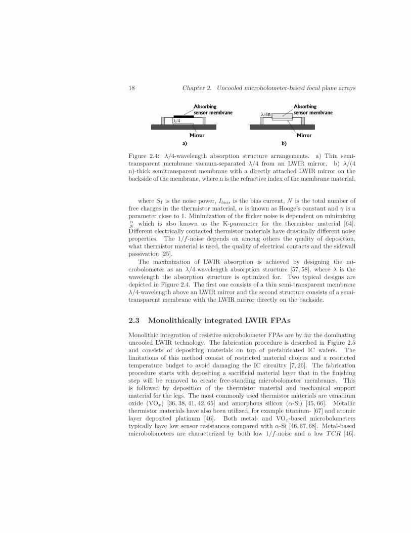
The maximization of LWIR absorption is achieved by designing the mi-crobolometer as an λ/4-wavelength absorption structure [57, 58], where λ is thewavelength the absorption structure is optimized for. Two typical designs aredepicted in Figure 2.4. The first one consists of a thin semi-transparent membraneλ/4-wavelength above an LWIR mirror and the second structure consists of a semi-transparent membrane with the LWIR mirror directly on the backside.
2.3 Monolithically integrated LWIR FPAs
Monolithic integration of resistive microbolometer FPAs are by far the dominatinguncooled LWIR technology. The fabrication procedure is described in Figure 2.5and consists of depositing materials on top of prefabricated IC wafers. Thelimitations of this method consist of restricted material choices and a restrictedtemperature budget to avoid damaging the IC circuitry [7, 26]. The fabricationprocedure starts with depositing a sacrificial material layer that in the finishingstep will be removed to create free-standing microbolometer membranes. Thisis followed by deposition of the thermistor material and mechanical supportmaterial for the legs. The most commonly used thermistor materials are vanadiumoxide (VOx) [36, 38, 41, 42, 65] and amorphous silicon (α-Si) [45, 66]. Metallicthermistor materials have also been utilized, for example titanium- [67] and atomiclayer deposited platinum [46]. Both metal- and VOx-based microbolometerstypically have low sensor resistances compared with α-Si [46, 67, 68]. Metal-basedmicrobolometers are characterized by both low 1/f -noise and a low TCR [46].
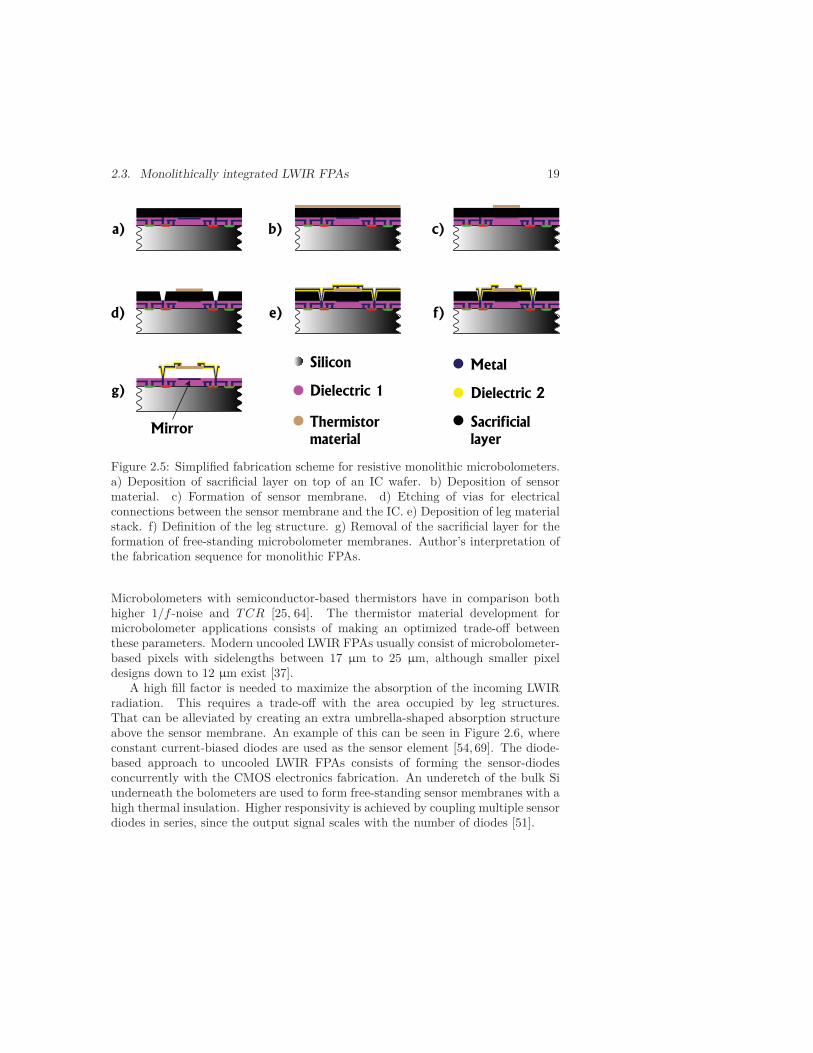
2.3. Monolithically integrated LWIR FPAs 19
Silicon
Dielectric 1 Dielectric 2
Metal
a)
f)e)d)
b)
Thermistor
material
Sacrificial
layer
c)
g)
Mirror
Figure 2.5: Simplified fabrication scheme for resistive monolithic microbolometers.a) Deposition of sacrificial layer on top of an IC wafer. b) Deposition of sensormaterial. c) Formation of sensor membrane. d) Etching of vias for electricalconnections between the sensor membrane and the IC. e) Deposition of leg materialstack. f) Definition of the leg structure. g) Removal of the sacrificial layer for theformation of free-standing microbolometer membranes. Author’s interpretation ofthe fabrication sequence for monolithic FPAs.
Microbolometers with semiconductor-based thermistors have in comparison bothhigher 1/f -noise and TCR [25, 64]. The thermistor material development formicrobolometer applications consists of making an optimized trade-off betweenthese parameters. Modern uncooled LWIR FPAs usually consist of microbolometer-based pixels with sidelengths between 17 μm to 25 μm, although smaller pixeldesigns down to 12 μm exist [37].
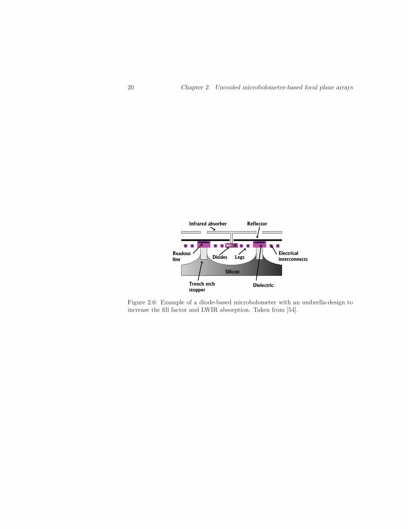
A high fill factor is needed to maximize the absorption of the incoming LWIRradiation. This requires a trade-off with the area occupied by leg structures.That can be alleviated by creating an extra umbrella-shaped absorption structureabove the sensor membrane. An example of this can be seen in Figure 2.6, whereconstant current-biased diodes are used as the sensor element [54, 69]. The diode-based approach to uncooled LWIR FPAs consists of forming the sensor-diodesconcurrently with the CMOS electronics fabrication. An underetch of the bulk Siunderneath the bolometers are used to form free-standing sensor membranes with ahigh thermal insulation. Higher responsivity is achieved by coupling multiple sensordiodes in series, since the output signal scales with the number of diodes [51].
20 Chapter 2. Uncooled microbolometer-based focal plane arrays
Readout
line
Trench etch
stopper
Infrared absorber
Diodes
Reflector
LegsElectrical
interconnects
Silicon
Dielectric
Figure 2.6: Example of a diode-based microbolometer with an umbrella-design toincrease the fill factor and LWIR absorption. Taken from [54].
2.4. Heterogeneous integration of LWIR FPAs 21
2.4 Heterogeneous integration of LWIR FPAs
In this approach (presented in Paper 1 and Paper 2 ), a monocrystalline Si/SiGequantum-well based material is used as the microbolometer thermistor material.This thermistor material is attractive due to its combination of high TCR around3 %/K [25] and low electronic noise compared with VOx and α-Si [64, 70]. Themonocrystalline structure of the Si/SiGe quantum-well based material decreasesthe magnitude of 1/f-noise compared with thermistors made from poly-crystallineand amorphous materials and the SiGe quantum wells increase the temperaturedependence of resistance [70]. However, the thermistor material is grown withepitaxial methods and requires a high deposition temperature of more than600 ◦C [64]. This is above the temperature budget of readout ICs. The only methodfor SoC-integration of this kind of material with ICs is thus separate fabricationof the thermistor material, followed by heterogeneous integration of the thermistorwafer with an IC wafer. The thermistor is also used as the absorption structure inthe microbolometer design.
2.4.1 Microbolometer Design
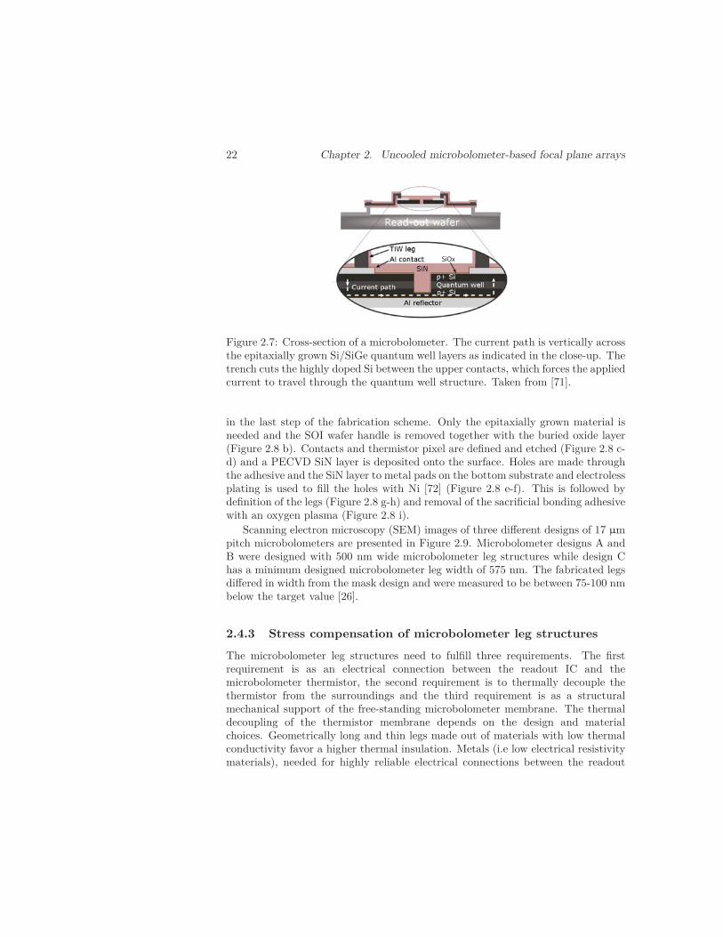
Heterogeneously integrated microbolometer FPAs are designed for applicationsin the 8-14 μm wavelength spectral range and the infrared absorption of themicrobolometer is optimized by designing it as an optical λ/4-cavity [57]. Theoptical cavity consists of a bottom Al mirror, epitaxially grown Si/SiGe andplasma enhanced chemical vapor deposited (PECVD) SiOx and silicon nitride(SiN) passivation layers. A schematic cross-section of a microbolometer pixel isshown in Figure 2.3. The microbolometer leg structures consist of a sandwichstructure SiN, titanium tungsten (TiW) and SiN to both stress compensate the legand to encapsulate the thin TiW film that provides the electrical contact betweenelectroless plated nickel (Ni) pillars and the thermistor material. The legs connectto deposited Al contacts on the Si/SiGe thermistor material. An etched trenchdisconnects the two top contacts on the Si/SiGe thermistor material from eachother through the uppermost highly doped Si contact layer. This is used to guidethe current vertically through the horizontally arranged Si/SiGe quantum wells ofthe microbolometer membrane [26]. A depiction of the microbolometer cross-sectionis shown in Figure 2.7 together with the electrical current path.
2.4.2 Fabrication sequence
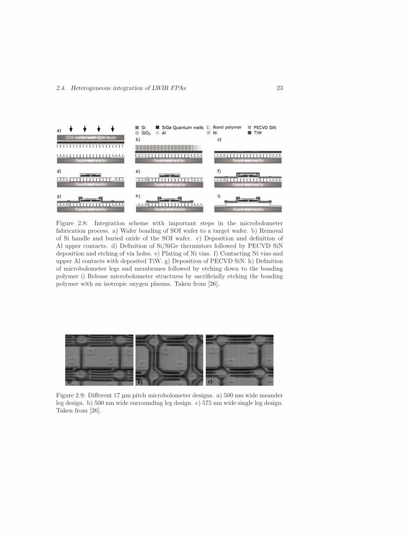
An overview of the most important steps to realize very large scale heterogeneousintegration for LWIR microbolometer arrays is presented in Figure 2.8. The startingmaterials consist of a readout-wafer with electrical interconnects and a SOI waferwith the epitaxially grown Si/SiGe quantum-well material stack. The wafers areadhesive wafer bonded to each other with a 3 μm thick polymer layer (mr-I 9150,Micro Resist Technology GmbH). This is a sacrificial layer that will be removed
22 Chapter 2. Uncooled microbolometer-based focal plane arrays
SiOx
Figure 2.7: Cross-section of a microbolometer. The current path is vertically acrossthe epitaxially grown Si/SiGe quantum well layers as indicated in the close-up. Thetrench cuts the highly doped Si between the upper contacts, which forces the appliedcurrent to travel through the quantum well structure. Taken from [71].
in the last step of the fabrication scheme. Only the epitaxially grown material isneeded and the SOI wafer handle is removed together with the buried oxide layer(Figure 2.8 b). Contacts and thermistor pixel are defined and etched (Figure 2.8 c-d) and a PECVD SiN layer is deposited onto the surface. Holes are made throughthe adhesive and the SiN layer to metal pads on the bottom substrate and electrolessplating is used to fill the holes with Ni [72] (Figure 2.8 e-f). This is followed bydefinition of the legs (Figure 2.8 g-h) and removal of the sacrificial bonding adhesivewith an oxygen plasma (Figure 2.8 i).
Scanning electron microscopy (SEM) images of three different designs of 17 μmpitch microbolometers are presented in Figure 2.9. Microbolometer designs A andB were designed with 500 nm wide microbolometer leg structures while design Chas a minimum designed microbolometer leg width of 575 nm. The fabricated legsdiffered in width from the mask design and were measured to be between 75-100 nmbelow the target value [26].
2.4.3 Stress compensation of microbolometer leg structures
The microbolometer leg structures need to fulfill three requirements. The firstrequirement is as an electrical connection between the readout IC and themicrobolometer thermistor, the second requirement is to thermally decouple thethermistor from the surroundings and the third requirement is as a structuralmechanical support of the free-standing microbolometer membrane. The thermaldecoupling of the thermistor membrane depends on the design and materialchoices. Geometrically long and thin legs made out of materials with low thermalconductivity favor a higher thermal insulation. Metals (i.e low electrical resistivitymaterials), needed for highly reliable electrical connections between the readout
2.4. Heterogeneous integration of LWIR FPAs 23
Figure 2.8: Integration scheme with important steps in the microbolometerfabrication process. a) Wafer bonding of SOI wafer to a target wafer. b) Removalof Si handle and buried oxide of the SOI wafer. c) Deposition and definition ofAl upper contacts. d) Definition of Si/SiGe thermistors followed by PECVD SiNdeposition and etching of via holes. e) Plating of Ni vias. f) Contacting Ni vias andupper Al contacts with deposited TiW. g) Deposition of PECVD SiN. h) Definitionof microbolometer legs and membranes followed by etching down to the bondingpolymer i) Release microbolometer structures by sacrificially etching the bondingpolymer with an isotropic oxygen plasma. Taken from [26].
a) b) c)
Figure 2.9: Different 17 μm pitch microbolometer designs. a) 500 nm wide meanderleg design. b) 500 nm wide surrounding leg design. c) 575 nm wide single leg design.Taken from [26].
24 Chapter 2. Uncooled microbolometer-based focal plane arrays
IC and the individual bolometers, are characterized by high thermal conductivitysince the same mobile electrons that participate in the electrical conduction alsoparticipate in the heat transfer. This implies that the leg structures should bedesigned with as thin metal layer for electrical connections as possible to minimizethe thermal conductance from the microbolometer membrane. The requirementfor mechanical support of the free-standing thermistor membrane is solved by theintroduction of a dielectric support material with a low thermal conductivity. In thedesign presented in Paper 1 and Paper 2 TiW was used as the electrical connectionmaterial and SiN as the structural material. Figure 2.10 depicts the fabricationsequence in detail. SiN is deposited in two separate layers around the TiW metallayer in the formation of a three-layer leg structures. This is due to the differentinternal stress properties of the deposited layers, where a symmetrical leg-stackcomposition (SiN/TiW/SiN) is easier to stress-compensate than structures basedon two layers with different material properties. The first SiN layer is deposited ontop of the bonding polymer, followed by the deposition of a TiW layer. This two-layer structure is sensitive to temperatures above 110 ◦C and experienced changesin stress properties without proper precaution. Temperatures above 110 ◦C occursduring the second SiN layer deposition. The TiW layer was therefore etched intosmaller stipes of TiW. This alleviated the problem with uncontrolled changes ofthe stress properties. Figure 2.11 is a microscopy image of a deposited triple stackwhere a mask design based on too large TiW islands resulted in changed stressproperties [26]. Figure 2.12 shows a comparison between two test designs of TiWislands together with the layer thicknesses used in the actual microbolometer arrayfabrication (150 nm lower SiN, 50 nm TiW, 200 nm upper SiN). The structures inFigure 2.12 a was defined on a large rectangular (170 μm × 230 μm) TiW islandbetween two SiN layers and resulted in test structure fingers bending downwards.The structures in Figure 2.12 b had the same finger design but is instead definedand etched on smaller 4 μm wide stripes of TiW, one for each finger, that avoidstoo severe bimaterial induced changes of the mechanical properties. This results infingers bending upwards [26].
2.4.4 Characterization of resistive microbolometers
2.4.4.1 Resistive properties
TCR is recorded by measuring the resistance of individual microbolometers atdifferent temperatures. Resistive heating occurs during readout and the resistancemeasurement preferably is performed by applying short square-wave voltage pulsesin atmospheric pressure to avoid excessive heating. Resistance and TCR for amicrobolometer is given by:
2.4. Heterogeneous integration of LWIR FPAs 25
a) b) c)
d) e) f )
SiN layer 1
TiW layer
Resist mask
SiN layer 2
Bond polymer
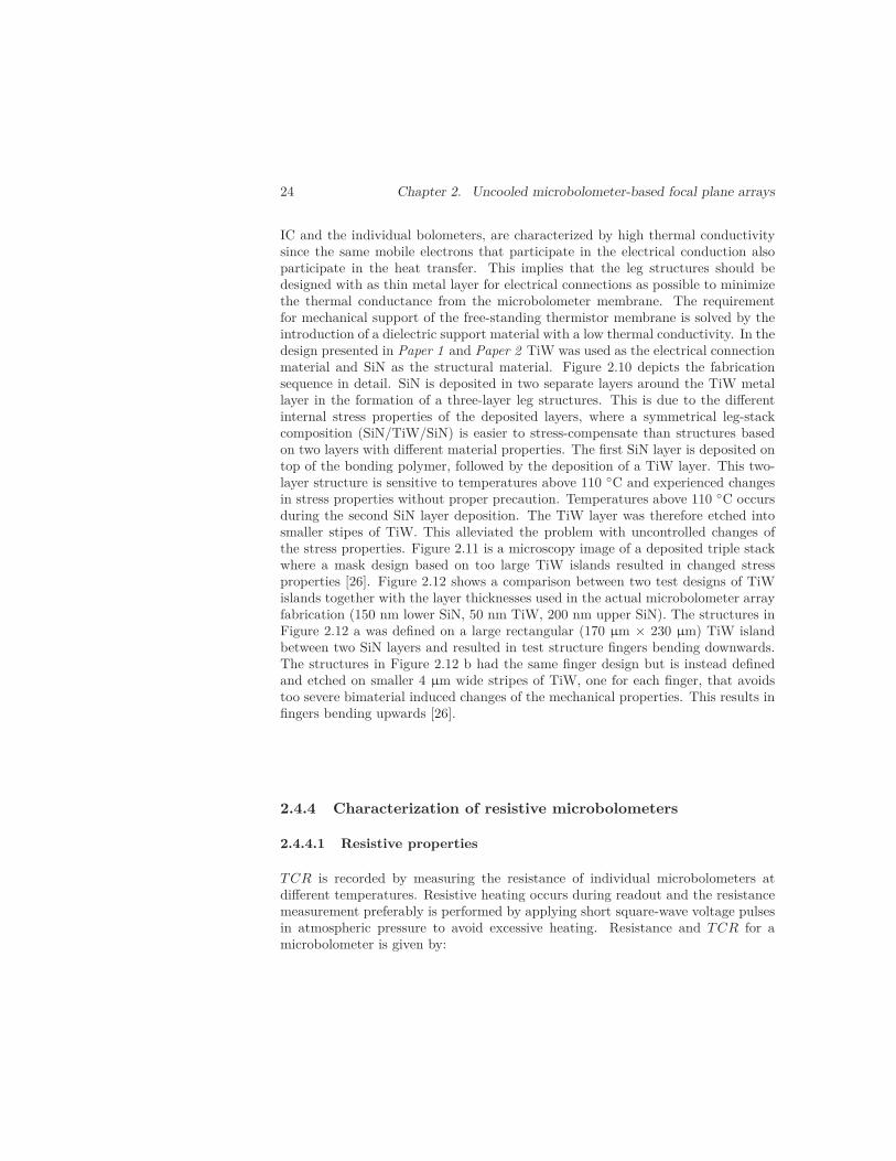
Figure 2.10: Fabrication sequence for microbolometer leg structures. a) SiN layeris deposited on top of bonding polymer. b)-c) TiW is deposited and masked intoislands and etched down to the SiN layer. d) Second SiN layer is deposited. e)The TiW islands are masked into the final leg structure design. f) The triple stackis etched to the bonding polymer, forming the final microbolometer leg structure.Taken from [26].
PECVD silicon nitride
Large rectangular area covered with titanium tungstenlayer
Test mask withfinger structure
Stress induced fringes in silicon nitride layer
170 μm
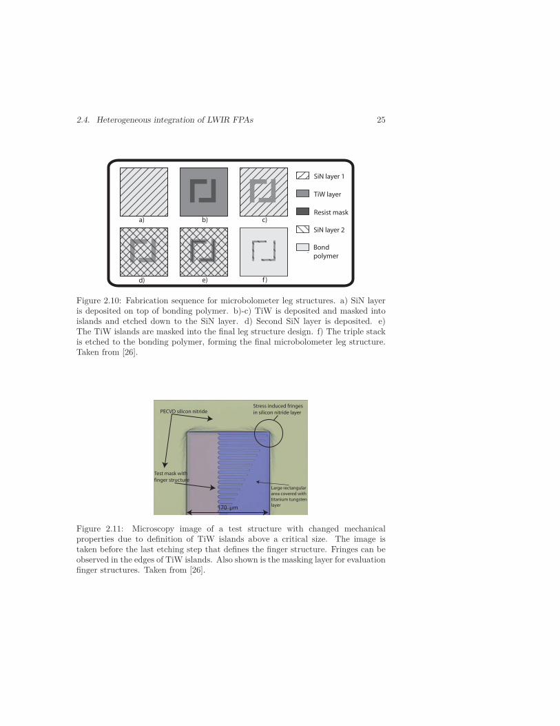
Figure 2.11: Microscopy image of a test structure with changed mechanicalproperties due to definition of TiW islands above a critical size. The image istaken before the last etching step that defines the finger structure. Fringes can beobserved in the edges of TiW islands. Also shown is the masking layer for evaluationfinger structures. Taken from [26].
26 Chapter 2. Uncooled microbolometer-based focal plane arrays
a) b)
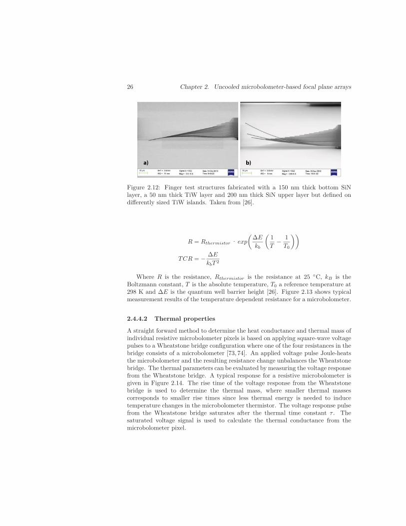
Figure 2.12: Finger test structures fabricated with a 150 nm thick bottom SiNlayer, a 50 nm thick TiW layer and 200 nm thick SiN upper layer but defined ondifferently sized TiW islands. Taken from [26].
R = Rthermistor · exp
(ΔE
kb
(1T
− 1T0
))
TCR = − ΔE
kbT 2
Where R is the resistance, Rthermistor is the resistance at 25 ◦C, kB is theBoltzmann constant, T is the absolute temperature, T0 a reference temperature at298 K and ΔE is the quantum well barrier height [26]. Figure 2.13 shows typicalmeasurement results of the temperature dependent resistance for a microbolometer.
2.4.4.2 Thermal properties
A straight forward method to determine the heat conductance and thermal mass ofindividual resistive microbolometer pixels is based on applying square-wave voltagepulses to a Wheatstone bridge configuration where one of the four resistances in thebridge consists of a microbolometer [73, 74]. An applied voltage pulse Joule-heatsthe microbolometer and the resulting resistance change unbalances the Wheatstonebridge. The thermal parameters can be evaluated by measuring the voltage responsefrom the Wheatstone bridge. A typical response for a resistive microbolometer isgiven in Figure 2.14. The rise time of the voltage response from the Wheatstonebridge is used to determine the thermal mass, where smaller thermal massescorresponds to smaller rise times since less thermal energy is needed to inducetemperature changes in the microbolometer thermistor. The voltage response pulsefrom the Wheatstone bridge saturates after the thermal time constant τ . Thesaturated voltage signal is used to calculate the thermal conductance from themicrobolometer pixel.
2.4. Heterogeneous integration of LWIR FPAs 27
3 3.05 3.1 3.15 3.2 3.25 3.3 3.35
x 10−3
10
10.2
10.4
10.6
10.8
11
11.2
1 / T [K−1]
Log(
R)
Arrhenius plot of resistance vs. temperature
TCR = − 2.9 % / K
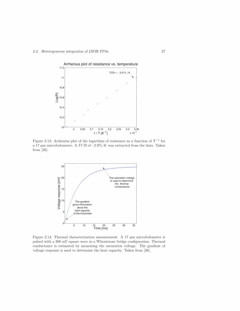
Figure 2.13: Arrhenius plot of the logarithm of resistance as a function of T−1 fora 17 μm microbolometer. A TCR of - 2.9%/K was extracted from the data. Takenfrom [26].
5 10 15 20 25 30 350
5
10
15
20
25
Time [ms]
Vol
tage
res
pons
e [m
V]
The gradient gives information
about the heat capacity
of the bolometer
The saturation voltage is used to determine
the thermal conductance
Figure 2.14: Thermal characterization measurement. A 17 μm microbolometer ispulsed with a 300 mV square wave in a Wheatstone bridge configuration. Thermalconductance is estimated by measuring the saturation voltage. The gradient ofvoltage response is used to determine the heat capacity. Taken from [26].
28 Chapter 2. Uncooled microbolometer-based focal plane arrays
Spectrum
Analyzer
V
bias
Devic
e u
nder
test
R_devic
e
Current
Amplifier
R
C
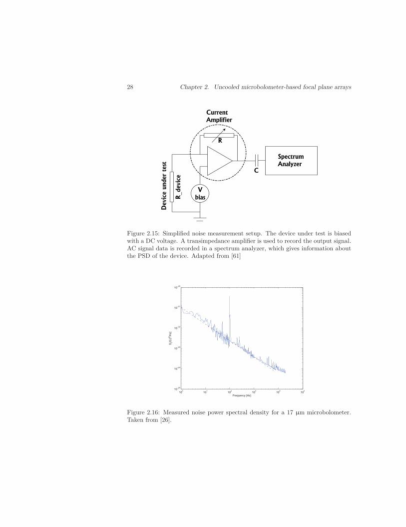
Figure 2.15: Simplified noise measurement setup. The device under test is biasedwith a DC voltage. A transimpedance amplifier is used to record the output signal.AC signal data is recorded in a spectrum analyzer, which gives information aboutthe PSD of the device. Adapted from [61]
100
101
102
103
104
105
10−25
10−24
10−23
10−22
10−21
10−20
Frequency [Hz]
SI(f
) [I2 /H
z]
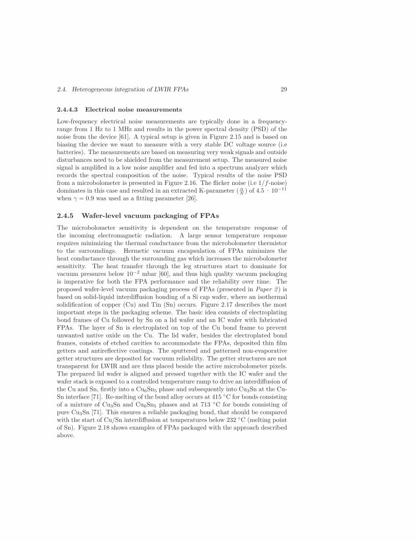
Figure 2.16: Measured noise power spectral density for a 17 μm microbolometer.Taken from [26].
2.4. Heterogeneous integration of LWIR FPAs 29
2.4.4.3 Electrical noise measurements
Low-frequency electrical noise measurements are typically done in a frequency-range from 1 Hz to 1 MHz and results in the power spectral density (PSD) of thenoise from the device [61]. A typical setup is given in Figure 2.15 and is based onbiasing the device we want to measure with a very stable DC voltage source (i.ebatteries). The measurements are based on measuring very weak signals and outsidedisturbances need to be shielded from the measurement setup. The measured noisesignal is amplified in a low noise amplifier and fed into a spectrum analyzer whichrecords the spectral composition of the noise. Typical results of the noise PSDfrom a microbolometer is presented in Figure 2.16. The flicker noise (i.e 1/f -noise)dominates in this case and resulted in an extracted K-parameter ( α
N ) of 4.5 · 10−11
when γ = 0.9 was used as a fitting parameter [26].
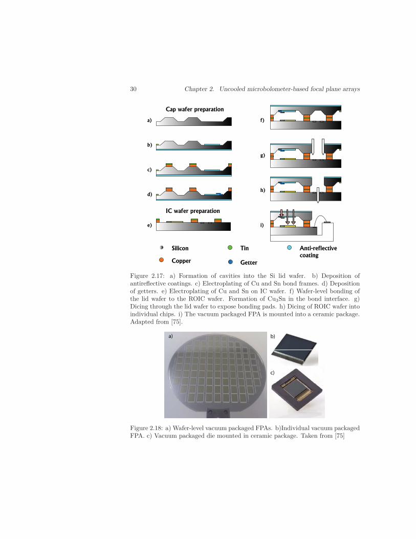
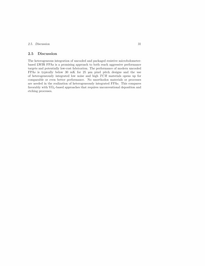
2.4.5 Wafer-level vacuum packaging of FPAs
The microbolometer sensitivity is dependent on the temperature response ofthe incoming electromagnetic radiation. A large sensor temperature responserequires minimizing the thermal conductance from the microbolometer thermistorto the surroundings. Hermetic vacuum encapsulation of FPAs minimizes theheat conductance through the surrounding gas which increases the microbolometersensitivity. The heat transfer through the leg structures start to dominate forvacuum pressures below 10−2 mbar [60], and thus high quality vacuum packagingis imperative for both the FPA performance and the reliability over time. Theproposed wafer-level vacuum packaging process of FPAs (presented in Paper 2 ) isbased on solid-liquid interdiffusion bonding of a Si cap wafer, where an isothermalsolidification of copper (Cu) and Tin (Sn) occurs. Figure 2.17 describes the mostimportant steps in the packaging scheme. The basic idea consists of electroplatingbond frames of Cu followed by Sn on a lid wafer and an IC wafer with fabricatedFPAs. The layer of Sn is electroplated on top of the Cu bond frame to preventunwanted native oxide on the Cu. The lid wafer, besides the electroplated bondframes, consists of etched cavities to accommodate the FPAs, deposited thin filmgetters and antireflective coatings. The sputtered and patterned non-evaporativegetter structures are deposited for vacuum reliability. The getter structures are nottransparent for LWIR and are thus placed beside the active microbolometer pixels.The prepared lid wafer is aligned and pressed together with the IC wafer and thewafer stack is exposed to a controlled temperature ramp to drive an interdiffusion ofthe Cu and Sn, firstly into a Cu6Sn5 phase and subsequently into Cu3Sn at the Cu-Sn interface [71]. Re-melting of the bond alloy occurs at 415 ◦C for bonds consistingof a mixture of Cu3Sn and Cu6Sn5 phases and at 713 ◦C for bonds consisting ofpure Cu3Sn [71]. This ensures a reliable packaging bond, that should be comparedwith the start of Cu/Sn interdiffusion at temperatures below 232 ◦C (melting pointof Sn). Figure 2.18 shows examples of FPAs packaged with the approach describedabove.
30 Chapter 2. Uncooled microbolometer-based focal plane arrays
Cap wafer preparation
IC wafer preparation
a)
h)
g)
f)
e)
d)
c)
b)
i)
Silicon
Copper
Anti-reflective
coating
Tin
Getter
Figure 2.17: a) Formation of cavities into the Si lid wafer. b) Deposition ofantireflective coatings. c) Electroplating of Cu and Sn bond frames. d) Depositionof getters. e) Electroplating of Cu and Sn on IC wafer. f) Wafer-level bonding ofthe lid wafer to the ROIC wafer. Formation of Cu3Sn in the bond interface. g)Dicing through the lid wafer to expose bonding pads. h) Dicing of ROIC wafer intoindividual chips. i) The vacuum packaged FPA is mounted into a ceramic package.Adapted from [75].
a)
c)
b)
Figure 2.18: a) Wafer-level vacuum packaged FPAs. b)Individual vacuum packagedFPA. c) Vacuum packaged die mounted in ceramic package. Taken from [75]
2.5. Discussion 31
2.5 Discussion
The heterogeneous integration of uncooled and packaged resistive microbolometer-based LWIR FPAs is a promising approach to both reach aggressive performancetargets and potentially low-cost fabrication. The performance of modern uncooledFPAs is typically below 30 mK for 25 μm pixel pitch designs and the useof heterogeneously integrated low noise and high TCR materials opens up forcomparable or even better performance. No unorthodox materials or processesare needed in the realization of heterogeneously integrated FPAs. This comparesfavorably with VOx-based approaches that requires unconventional deposition andetching processes.

Chapter 3
Evaluation of bond energy inadhesive wafer bonding
3.1 Introduction
In adhesive wafer bonding, an adhesive layer is deposited on one or both of thewafers with a suitable deposition technique (i.e spin coating, laminating, sprayingetc.). The wafers are brought into intimate contact and the intermediate adhesiveis typically cured by the application of heat and pressure in a specialized waferbonding tool [76]. Advantages of adhesive wafer bonding include IC compatibilitydue to relatively low adhesive curing temperatures, a wide design window for thethicknesses of the deposited polymer coating and an insensitivity to particles andsurface topology due to plastic reflow and deformation of the polymer adhesiveat the bond interface [76]. A large variety of different substrate materials canbe joined with adhesive wafer bonding since the typical polymers used adhere tomost materials [76]. Adhesive wafer bonding is the enabling technology used in thefabrication of uncooled LWIR FPAs in Paper 1 and Paper 2 and is also used totransfer and attach expanded arrays of dies as described in Paper 6 and aluminafilters as described in Paper 5. Paper 3 presents an in-depth description in howa nano-imprint resist can be used as a sacrificial adhesive for the fabrication ofMEMS.
There are a vast variety of polymers that have been evaluated for adhesive waferbonding, such as polyimides [77,78], epoxies [79–81], benzocyclobutene (BCB) [82–86], UV-curable epoxies (i.e SU8) [87–92] and nano-imprint resists [76, 93]. Easeof application, bond interface quality, bond hermeticity, curing temperature andthe bond strength are important parameters to consider when choosing a polymeradhesive [76]. Furthermore, some adhesives are permanent structural layers thatare hard to remove (i.e BCB), while other adhesives have the capability to be usedas sacrificial material layers (i.e mr-I 9000XP-series).
33
34 Chapter 3. Evaluation of bond energy in adhesive wafer bonding
Tensile Force
Tensile Force
Shear Force
Shear Force Adhesive
Wafer 1
Wafer 2 Blade
Wafer 1
Wafer 2
ForceForce
Wafer 1
Wafer 2
Pressure
Wafer 1
Wafer 2 Wafer 2
a) b)
c) d)
Figure 3.1: a) Tensile and shear load tests. b) Crack opening tests. c) Four-pointbending tests. d) Blister tests.
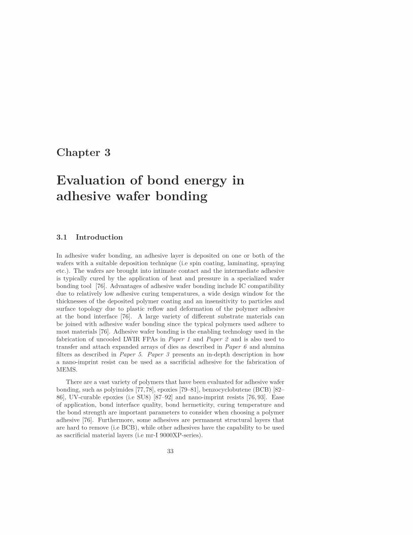
3.2 Methods for evaluating bond energy
Figure 3.1 illustrates four different techniques to estimate the bond strength. Thesetechniques are by their very nature destructive. Tests based on tensile loading ofthe bond interface measures the tensile strength of a bond while tests based oncontrolled opening cracks and blister tests measures the surface energies of bonds.
3.2.1 Tensile and shear load measurements
This method is depicted in Figure 3.1 a and is based on pulling apart bondedsamples by the application of tensile of shear forces. The tensile strength is definedas the fracture force divided by the sample area (unit, Pa) [76].
3.2.2 Crack opening method
This technique is based on introducing a sharp spacer (i.e razor blade) of a definedthickness into the bond interface of a sample (Figure 3.1 b). The bond willdelaminate and the length of the resulting crack is measured. Information aboutthe thicknesses of the bonded plates, the material parameters and the length of thedelaminated crack is related to the surface bond energy (unit, J/m2) [76].
3.3. Blister test evaluation platform 35
3.2.3 Four-point bending tests
This method is illustrated in Figure 3.1 c and is based on rectangular samples,where one of the substrates contains a pre-fabricated slit. The rectangular sampleis put in a fixture and loads are applied on fixed distances from the slit. The load-induced displacement is recorded. As the load is applied, the bending moment inthe slit area increases. When the applied load reaches a critical value, a bending-induced crack initiates at the tip of the slit and propagates along the weak interface.The measurement data is used together with mechanical beam theory to derive anexpression for the surface bond energy [83].
3.2.4 Blister tests
The test sample consists of a lid, bonded to a substrate with a hole (Figure 3.1 d).The substrate with the hole is fixed and attached to a pressure reservoir. Thepressure in the reservoir is increased until the lid is delaminated from the fixedsubstrate. The critical pressure to drive the delamination is mathematically relatedto the bond energy [94].
3.3 Blister test evaluation platform
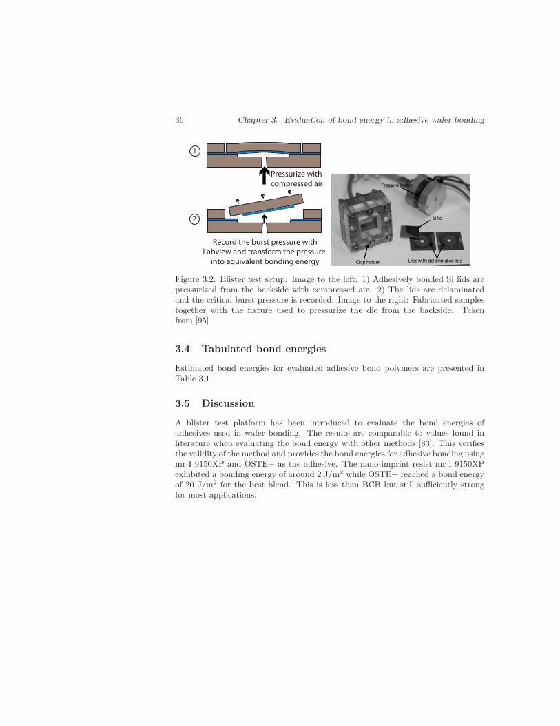
Paper 4 introduces a platform that was used for blister test evaluations of thebond energy for samples bonded with different polymer adhesives. The platform isdepicted in Figure 3.2 a and b. It is based upon two Si wafers adhesively bonded toeach other, where one of the wafer has pre-etched through holes. The bonded waferstack is diced and placed into a holder, followed by the application of increased gaspressure from the backside until the lid delaminates.
The pressure at the start of delamination (burst pressure) can be converted intoa bond energy per unit area according to [94]:
Pcr =(
32Eγah3
3a4(1 − ν2)
) 12
Where Pcr is the burst pressure, h is the wafer thickness of the lid, a is theradius of the circular cavity, ν is the Poisson’s ratio, E is the Young’s modulus forSi and γa is the adhesive fracture energy per unit area. The equation is deducedfrom Clapeiron’s theorem [94] and holds for diaphragms that deform elastically andthat are thin compared to the diameter of the circular cavity. The critical pressureneeded to delaminate the lid decreases with increased diameter of the circular cavity.The highest pressure needed for delamination is thus reached when delaminationof the lid starts, thereby driving the delamination to the edges of the lid, where itis torn off from the die.
36 Chapter 3. Evaluation of bond energy in adhesive wafer bonding
Pressurize with
compressed air
Record the burst pressure with
Labview and transform the pressure
into equivalent bonding energy
1
2
Chip holder Dies with delaminated lids
Pressure sensor
Si lid
Figure 3.2: Blister test setup. Image to the left: 1) Adhesively bonded Si lids arepressurized from the backside with compressed air. 2) The lids are delaminatedand the critical burst pressure is recorded. Image to the right: Fabricated samplestogether with the fixture used to pressurize the die from the backside. Takenfrom [95]
3.4 Tabulated bond energies
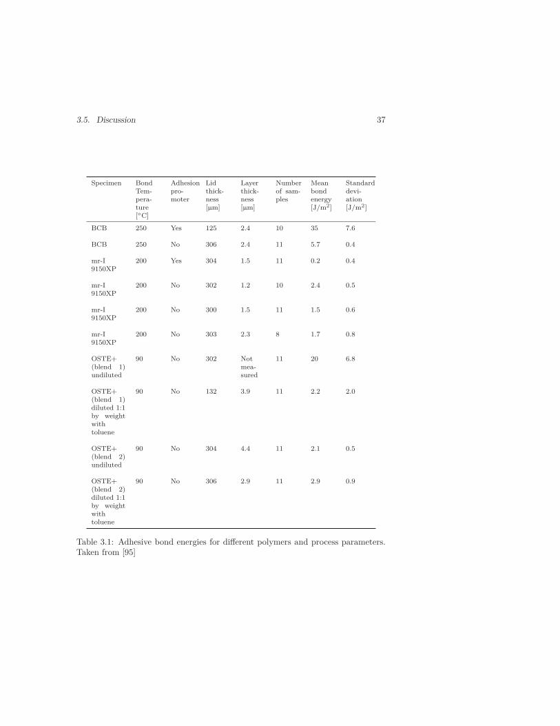
Estimated bond energies for evaluated adhesive bond polymers are presented inTable 3.1.
3.5 Discussion
A blister test platform has been introduced to evaluate the bond energies ofadhesives used in wafer bonding. The results are comparable to values found inliterature when evaluating the bond energy with other methods [83]. This verifiesthe validity of the method and provides the bond energies for adhesive bonding usingmr-I 9150XP and OSTE+ as the adhesive. The nano-imprint resist mr-I 9150XPexhibited a bonding energy of around 2 J/m2 while OSTE+ reached a bond energyof 20 J/m2 for the best blend. This is less than BCB but still sufficiently strongfor most applications.
3.5. Discussion 37
Specimen BondTem-pera-ture[◦C]
Adhesionpro-moter
Lidthick-ness[μm]
Layerthick-ness[μm]
Numberof sam-ples
Meanbondenergy[J/m2]
Standarddevi-ation[J/m2]
BCB 250 Yes 125 2.4 10 35 7.6
BCB 250 No 306 2.4 11 5.7 0.4
mr-I9150XP
200 Yes 304 1.5 11 0.2 0.4
mr-I9150XP
200 No 302 1.2 10 2.4 0.5
mr-I9150XP
200 No 300 1.5 11 1.5 0.6
mr-I9150XP
200 No 303 2.3 8 1.7 0.8
OSTE+(blend 1)undiluted
90 No 302 Notmea-sured
11 20 6.8
OSTE+(blend 1)diluted 1:1by weightwithtoluene
90 No 132 3.9 11 2.2 2.0
OSTE+(blend 2)undiluted
90 No 304 4.4 11 2.1 0.5
OSTE+(blend 2)diluted 1:1by weightwithtoluene
90 No 306 2.9 11 2.9 0.9
Table 3.1: Adhesive bond energies for different polymers and process parameters.Taken from [95]

Chapter 4
Heterogeneous integration ofnanoporous membranes
4.1 Introduction
Controlled electrochemical processing methods have opened up for the fabrication ofwafer-sized nano-porous membranes in Si and alumina [96,97]. The electrochemicalprocesses that are utilized enable controlled pore-size tailoring in a range from nm toμm over wafer-scale samples. Nano-porous membranes have found use in numerousapplications such as filtering, sequencing, amplification and drug delivery due totheir ability to discriminate molecules based on size and interaction [96, 98–100].Furthermore, nanoporous materials are characterized by a very large internalsurface area, which make them suitable for binding surfaces in biosensing [101,102].However, the specialized electrochemical fabrication method of the membranes isvery different from the surface machining of Si and glass or the plastic moldingprocesses that are used for manufacturing typical microfluidic components. Thisincompatibility limits the appeal of monolithic integration of porous materialsinto systems, although there are reports of in situ-forming of porous Si inmicrochannels [103].
Transfer bonding of separately fabricated nano-porous membranes onto pre-fabricated microfluidic systems solves this incompatibility problem and opens upfor optimal fabrication of the needed sub-components. Heterogeneous integrationby transfer bonding has been used for the transfer of porous Si Bragg mirrorsonto a flexible polymer sheet using an intermediate PDMS stamp [104] and forthe transfer of a porous Si waveguide onto a glass substrate [105, 106]. Presentlyused methods for heterogeneous integration of separate nano-porous membranesinclude clamping and gluing [107,108]. These two methods tend to be low-yieldingsince the extremely fragile membranes tend to break when they are clamped andthey are prone to clogging when glued due to the capillary action of the porousmembranes. The method that is presented in Paper 5 use dry adhesive chip scale
39
40 Chapter 4. Heterogeneous integration of nanoporous membranes
bonding with OSTE+ (from Mercene Labs AB) to transfer fragile nano-porous Siand alumina membranes for filtering applications. This solves the fragility andclogging problem when attaching the membranes on a holder or use them as acomponent in microfluidic systems. OSTE+ is a dual-cure off-stoichiometry thiol-ene-epoxy polymer material. The first curing step is initiated by UV-exposure andresults in a chemical reaction between thiol and allyl monomers in OSTE+. Thisresults in a partially polymerized soft solid material. The surface of the partiallycured OSTE+ is ideal for direct dry bonding of different materials, since its softnessmakes it compliant to surface irregularities [109]. It is this property and mode thatis used for the dry bonding of prefabricated nano-porous membranes. A secondcuring step, where the thiol- and epoxy-components of OSTE+ reacts, hardensthe polymer. This reaction starts immediately after mixing, but proceeds slowly atroom temperature. The temperature can be increased to 70 ◦C for 2 h to acceleratethe second curing step. After the second cure, the OSTE+ polymer is stiff with aYoung’s modulus of 1.2 GPa. The OSTE+ chemistry and reaction mechanisms aredescribed in [109].
4.2 OSTE+ enabled transfer bonding of porous membranes
4.2.1 Transfer of nano-porous membranes to OSTE+ chips
One of the heterogeneous transfer methods presented in Paper 5 is based on moldingpartially cured OSTE+ chips containing holes. Figure 4.1 b shows the steps neededto realize molded partially cured OSTE+ chips. A PDMS mold is prepared anddefines the outer chip dimensions of 15 × 15 × 1 mm3. 800 μm diameter steel pinsare used to define vias through the chip. To avoid the formation of a residualsqueeze-film on top of the pins, a matching shadow mask printed onto a 1 mmthick polycarbonate sheet was aligned on top of the mold. The OSTE+ chip waspeeled off from the mold after the initial UV curing. At this stage, the surface ofthe OSTE+ is dry and sticky due to the presence of unreacted epoxy groups.
Both nano-porous alumina membranes and porous Si membranes were bondedto the chips. The basic outline of the transfer is depicted in Figure 4.1 c. The porousSi membranes were created in Si wafers, as shown in Figure 4.1 a and were deliveredin the form of 6 mm diameter and 30 μm thick porous Si membranes with 50%porosity and a pore size of 70 nm. The membranes are still partially attached to theSi substrate, although not directly underneath due to electrochemical underetchingof the membrane. The membrane was transferred by stamping the OSTE+ chiponto the porous Si and breaking it loose from the Si substrate followed by curingthe chips with transferred porous Si membranes. Nano-porous alumina membranes(Whatman AnoporeT M ) were transferred in a similar way, with the difference thatthese are less fragile and handled individually. Figure 4.2 shows images of OSTE+polymer chips with transferred porous Si and alumina membranes.
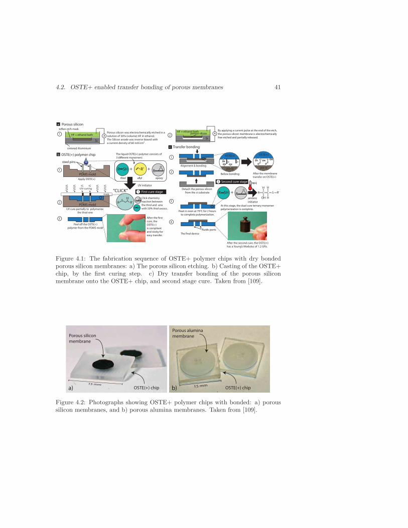
4.2. OSTE+ enabled transfer bonding of porous membranes 41
After the second cure, the OSTE(+)
has a Young’s Modulus of 1.2 GPa.
OSTE(+) polymer chip
PDMS mold
Apply OSTE(+)
UV curing
UV cure partially to polymerize
the thiol-ene
polymer from the PDMS mold
Transfer bonding
Alignment & bonding
Detach the porous silicon
from the si substrate
Heat in oven at 70ºC for 2 hours
to complete polymerization.
+ +R SH R’ R
O
thiol allyl epoxy
The liquid OSTE(+) polymer consists of
RS
H
R’
“CLICK”
Click chemistry
reaction between
the thiol and -ene
with 50% thiol excess.
UV initiator
R SH
1 First cure stage
2 Second cure stage
R
O
R
O
+
70˚C
R SH R’C C S
OH
H H
H
R
anionic
initiator
mask
SH OO
At this stage, the dual cure ternary monomer
polymerization is complete.
1
2
3
c
1
2
3
4cure, the
OSTE(+)
is compliant
and sticky for
easy transfer.
OH OH
OSTE(+)
por-Si
Before bonding
O
OSTE(+)
por-Si
c
cOH
Oc
c OHSH
After the membrane
transfer on OSTE(+)
Porous silicon
By applying a current pulse at the end of the etch,
the porous silicon membrane is electrochemically
free etched and partially released.
Si
sintered Aluminium
a
1 2HF + ethanol bath APorous silicon was electrochemically etched in a
solution of 30% (volume) HF in ethanol.
The Silicon anode was reverse biased with
a current density of 60 mA/cm .
Si
HF + ethanol bathAporous silicon
PDMS mold
b
steel pins
Figure 4.1: The fabrication sequence of OSTE+ polymer chips with dry bondedporous silicon membranes: a) The porous silicon etching. b) Casting of the OSTE+chip, by the first curing step. c) Dry transfer bonding of the porous siliconmembrane onto the OSTE+ chip, and second stage cure. Taken from [109].
Porous silicon
membrane
OSTE(+) chipa)
Porous alumina
membrane
OSTE(+) chipb)
Figure 4.2: Photographs showing OSTE+ polymer chips with bonded: a) poroussilicon membranes, and b) porous alumina membranes. Taken from [109].
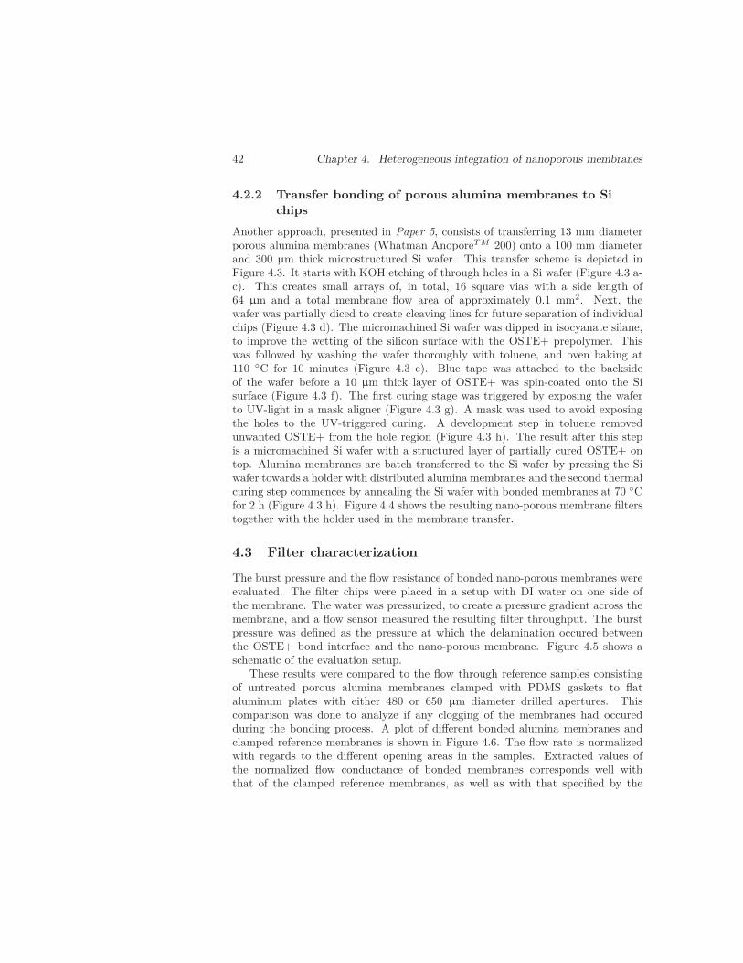
42 Chapter 4. Heterogeneous integration of nanoporous membranes
4.2.2 Transfer bonding of porous alumina membranes to Sichips
Another approach, presented in Paper 5, consists of transferring 13 mm diameterporous alumina membranes (Whatman AnoporeT M 200) onto a 100 mm diameterand 300 μm thick microstructured Si wafer. This transfer scheme is depicted inFigure 4.3. It starts with KOH etching of through holes in a Si wafer (Figure 4.3 a-c). This creates small arrays of, in total, 16 square vias with a side length of64 μm and a total membrane flow area of approximately 0.1 mm2. Next, thewafer was partially diced to create cleaving lines for future separation of individualchips (Figure 4.3 d). The micromachined Si wafer was dipped in isocyanate silane,to improve the wetting of the silicon surface with the OSTE+ prepolymer. Thiswas followed by washing the wafer thoroughly with toluene, and oven baking at110 ◦C for 10 minutes (Figure 4.3 e). Blue tape was attached to the backsideof the wafer before a 10 μm thick layer of OSTE+ was spin-coated onto the Sisurface (Figure 4.3 f). The first curing stage was triggered by exposing the waferto UV-light in a mask aligner (Figure 4.3 g). A mask was used to avoid exposingthe holes to the UV-triggered curing. A development step in toluene removedunwanted OSTE+ from the hole region (Figure 4.3 h). The result after this stepis a micromachined Si wafer with a structured layer of partially cured OSTE+ ontop. Alumina membranes are batch transferred to the Si wafer by pressing the Siwafer towards a holder with distributed alumina membranes and the second thermalcuring step commences by annealing the Si wafer with bonded membranes at 70 ◦Cfor 2 h (Figure 4.3 h). Figure 4.4 shows the resulting nano-porous membrane filterstogether with the holder used in the membrane transfer.
4.3 Filter characterization
The burst pressure and the flow resistance of bonded nano-porous membranes wereevaluated. The filter chips were placed in a setup with DI water on one side ofthe membrane. The water was pressurized, to create a pressure gradient across themembrane, and a flow sensor measured the resulting filter throughput. The burstpressure was defined as the pressure at which the delamination occured betweenthe OSTE+ bond interface and the nano-porous membrane. Figure 4.5 shows aschematic of the evaluation setup.
These results were compared to the flow through reference samples consistingof untreated porous alumina membranes clamped with PDMS gaskets to flataluminum plates with either 480 or 650 μm diameter drilled apertures. Thiscomparison was done to analyze if any clogging of the membranes had occuredduring the bonding process. A plot of different bonded alumina membranes andclamped reference membranes is shown in Figure 4.6. The flow rate is normalizedwith regards to the different opening areas in the samples. Extracted values ofthe normalized flow conductance of bonded membranes corresponds well withthat of the clamped reference membranes, as well as with that specified by the
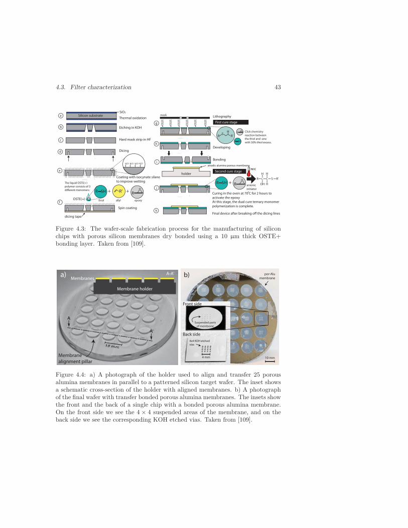
4.3. Filter characterization 43
k
mask
d
Second cure stage
R
O
+
70˚C
R SHR’C C S
OH
H H
H
R
anionic
initiator j
iBonding
RS
H
R’
Click chemistry
reaction between
the thiol and -ene
with 50% thiol excess.R SH
First cure stage
R
O
+ +R SH R’ R
O
thiol allyl epoxy
The liquid OSTE(+)
polymer consists of 3
NCO NCO NCO NCO
Silicon substratea
b
OSTE(+)f
g
Dicing
e
hc
Etching in KOH
Coating with isocynate silane
to improve wetting
Spin coating
Lithography
Developing
Curing in the oven at 70 C for 2 hours to
activate the epoxy
dicing tape
Thermal oxidation
Hard mask strip in HF
O
anodic alumina porous membrane
holder
SiO2
At this stage, the dual cure ternary monomer
polymerization is complete.
Figure 4.3: The wafer-scale fabrication process for the manufacturing of siliconchips with porous silicon membranes dry bonded using a 10 μm thick OSTE+bonding layer. Taken from [109].
a)
Membrane
alignment pillar
Membrane holder
MembranesA-A’
Back side
Front side
b)
4 mm 10 mm
Suspended parts
of membrane
4x4 KOH etched
vias
por-Alu
membrane
Figure 4.4: a) A photograph of the holder used to align and transfer 25 porousalumina membranes in parallel to a patterned silicon target wafer. The inset showsa schematic cross-section of the holder with aligned membranes. b) A photographof the final wafer with transfer bonded porous alumina membranes. The insets showthe front and the back of a single chip with a bonded porous alumina membrane.On the front side we see the 4 × 4 suspended areas of the membrane, and on theback side we see the corresponding KOH etched vias. Taken from [109].
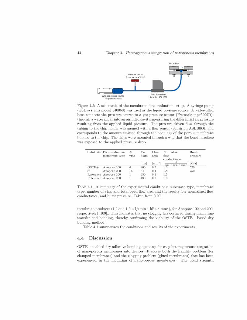
44 Chapter 4. Heterogeneous integration of nanoporous membranes
Syringe pressure sourceTSE Systems 540060
Pressure sensorFreescale mpx5999D
Fluid flow sensorSensirion ASL 1600
Chip holder
Figure 4.5: A schematic of the membrane flow evaluation setup. A syringe pump(TSE systems model 540060) was used as the liquid pressure source. A water-filledhose connects the pressure source to a gas pressure sensor (Freescale mpx5999D),through a water pillar into an air filled cavity, measuring the differential air pressureresulting from the applied liquid pressure. The pressure-driven flow through thetubing to the chip holder was gauged with a flow sensor (Sensirion ASL1600), andcorresponds to the amount emitted through the openings of the porous membranebonded to the chip. The chips were mounted in such a way that the bond interfacewas exposed to the applied pressure drop.
Substrate Porous aluminamembrane type
#vias
Viadiam.
Flowarea
Normalizedflowconductance
Burstpressure
[μm] [mm2] [ μlmin · kPa · mm2 ] [kPa]
OSTE+ Anopore 100 4 800 0.5 1.3 520Si Anopore 200 16 64 0.1 1.8 750Reference Anopore 100 1 650 0.3 1.5Reference Anopore 200 1 480 0.2 1.3
Table 4.1: A summary of the experimental conditions: substrate type, membranetype, number of vias, and total open flow area and the results for: normalized flowconductance, and burst pressure. Taken from [109].
membrane producer (1.2 and 1.5 μ l/(min · kPa · mm2), for Anopore 100 and 200,respectively) [109].. This indicates that no clogging has occurred during membranetransfer and bonding, thereby confirming the viability of the OSTE+ based drybonding method.
Table 4.1 summarizes the conditions and results of the experiments.
4.4 Discussion
OSTE+ enabled dry adhesive bonding opens up for easy heterogeneous integrationof nano-porous membranes into devices. It solves both the fragility problem (forclamped membranes) and the clogging problem (glued membranes) that has beenexperienced in the mounting of nano-porous membranes. The bond strength
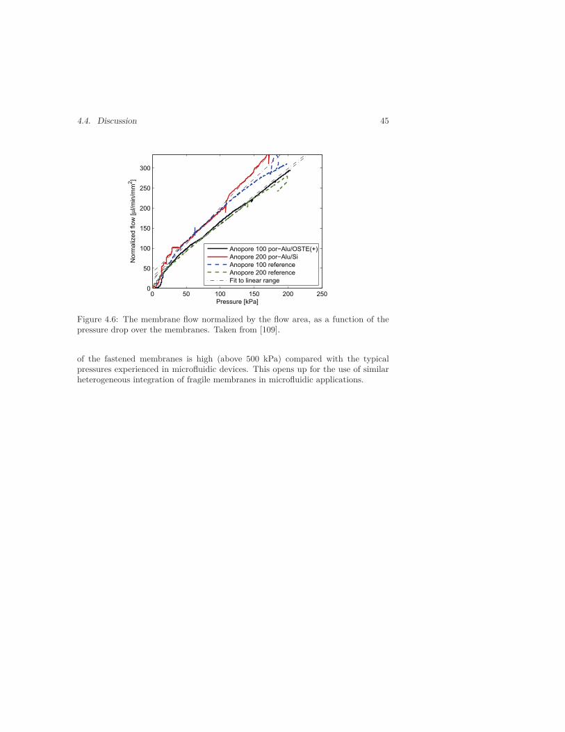
4.4. Discussion 45
0 50 100 150 200 2500
50
100
150
200
250
300
Pressure [kPa]
No
rma
lize
d flo
w [μ
l/m
in/m
m2]
Anopore 100 por−Alu/OSTE(+)
Anopore 200 por−Alu/Si
Anopore 100 reference
Anopore 200 reference
Fit to linear range
Figure 4.6: The membrane flow normalized by the flow area, as a function of thepressure drop over the membranes. Taken from [109].
of the fastened membranes is high (above 500 kPa) compared with the typicalpressures experienced in microfluidic devices. This opens up for the use of similarheterogeneous integration of fragile membranes in microfluidic applications.

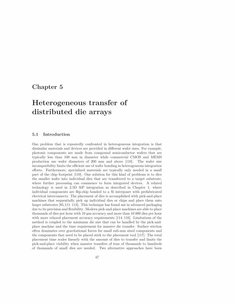
Chapter 5
Heterogeneous transfer ofdistributed die arrays
5.1 Introduction
One problem that is repeatedly confronted in heterogeneous integration is thatdissimilar materials and devices are provided in different wafer sizes. For example,photonic components are made from compound semiconductor wafers that aretypically less than 100 mm in diameter while commercial CMOS and MEMSproduction use wafer diameters of 200 mm and above [110]. The wafer sizeincompatibility limits the efficient use of wafer bonding in heterogeneous integrationefforts. Furthermore, specialized materials are typically only needed in a smallpart of the chip footprint [110]. One solution for this kind of problems is to dicethe smaller wafer into individual dies that are transferred to a target substrate,where further processing can commence to form integrated devices. A relatedtechnology is used in 2.5D SiP integration as described in Chapter 1, whereindividual components are flip-chip bonded to a Si interposer with prefabricatedelectrical interconnects. The placement of dies is accomplished with pick-and-placemachines that sequentially pick up individual dies or chips and place them ontolarger substrates [85,111–113]. This technique has found use in advanced packagingdue to its precision and flexibility. Modern pick-and-place machines are able to placethousands of dies per hour with 10 μm accuracy and more than 10 000 dies per hourwith more relaxed placement accuracy requirements [114–116]. Limitations of themethod is coupled to the minimum die size that can be handled by the pick-and-place machine and the time requirement for massive die transfer. Surface stictionoften dominates over gravitational forces for small sub-mm sized components andthe components that need to be placed stick to the placement tool [117]. The totalplacement time scales linearly with the amount of dies to transfer and limits thepick-and-place viability when massive transfers of tens of thousands to hundredsof thousands of small dies are needed. Two alternative approaches have been
47
48 Chapter 5. Heterogeneous transfer of distributed die arrays
Figure 5.1: a) Parallel transfer of dies. b) Sequential pick-and-place assembly.Taken from [110]
developed for spreading large amounts of small dies onto larger substrates. Theseare based on either self-assembly methods or parallel transfer methods.
5.2 Self-assembly methods
Self-assembly of dies and components are possible across large substrate areas.Available methods typically utilize either shape-matching, surface energy minimiza-tion or magnetic- or electric-field-mediated self-assembly [117]. Methods basedon shape-matching and surface energy minimization consist of structuring thedies and substrates in such a way that dies stick to preferred positions on thesubstrate. The basic arrangement consist of randomly spreading components ontoa structured substrate. Shaking the substrate enable the dies to move around untilthey find preferred positions that minimizes the surface interfacial energy or getplaced into structured cavities that fit with the dies size. Substrate structuringmethods include: Liquid solder-based self-assembly where specific solder pads onthe substrate matches metal pads on the dies [118,119], recess-based self-assemblymethods where only dies with the right size and shape fits into etched recessesin the target substrate [120] and capillary force-directed self-assembly that useshydrophilic/hydrophobic surface patterns [121]. These methods are also usedin combinations. For example, Stauth and Parviz presented a heterogeneousself-assembly process with shape matching where small dies or components areintroduced into a liquid medium [122]. Here, a structured wafer with solder insideshaped wells is put into the liquid and self-assembly occurs as the components firstfall into complementarily shaped wells and then become bound by the capillaryforces with the molten solder. In magnetic- and electric-field-mediated self-assembly, static magnetic and electric fields are used to assist the self-assemblyof components on substrates [117,123–125].
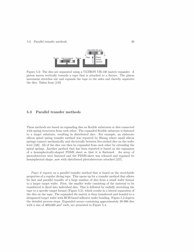
5.3. Parallel transfer methods 49
Fixture FixtureDies to expand
Piston
Tape
Expanded die array
Piston movesupward
Figure 5.2: The dies are separated using a ULTRON UH-130 matrix expander. Apiston moves vertically towards a tape that is attached to a fixture. The pistonmovement stretches out and expands the tape to the sides and thereby separatesthe dies. Taken from [110]
5.3 Parallel transfer methods
These methods are based on expanding dies on flexible substrates or dies connectedwith spring structures from each other. The expanded flexible substrate is fastenedto a target substrate, resulting in distributed dies. For example, an elaboratesilicon spiral spring transfer method was reported by Huang where small siliconsprings connect mechanically and electrically between free-etched dies on the waferlevel [126]. All of the dies can then be expanded from each other by extending thespiral springs. Another method that has been reported is based on the expansionof a hemispherically-shaped PDMS sheet so that it is flattened. An array ofphotodetectors were fastened and the PDMS-sheet was released and regained itshemispherical shape, now with distributed photodetectors attached [127].
Paper 6 reports on a parallel transfer method that is based on the stretchableproperties of a regular dicing tape. This opens up for a transfer method that allowsfor fast and parallel transfer of a large number of dies from a small wafer formatto a larger target wafer. First, the smaller wafer consisting of the material to betransferred is diced into individual dies. This is followed by radially stretching thetape to a specific target format (Figure 5.2), which results in a lateral separation ofthe dies on the tape. The expanded die matrix is then transferred and bonded to adesignated target wafer with BCB-based adhesive wafer bonding. Figure 5.3 depictsthe detailed process steps. Expanded arrays containing approximately 30 000 dieswith a size of 460x460 μm2 each, are presented in Figure 5.4.
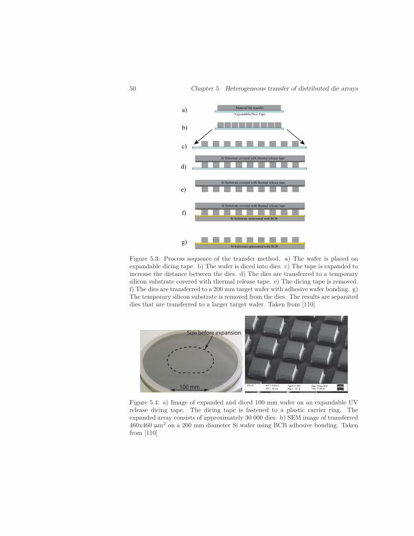
50 Chapter 5. Heterogeneous transfer of distributed die arrays
Expandable Dice Tape
Material for transfer
Si Substrate covered with thermal release tape
Si Substrate covered with thermal release tape
Si Substrate covered with thermal release tape
Si Substrate spincoated with BCB
Si Substrate spincoated with BCB
a)
b)
d)
c)
e)
f)
g)
Figure 5.3: Process sequence of the transfer method. a) The wafer is placed onexpandable dicing tape. b) The wafer is diced into dies. c) The tape is expanded toincrease the distance between the dies. d) The dies are transferred to a temporarysilicon substrate covered with thermal release tape. e) The dicing tape is removed.f) The dies are transferred to a 200 mm target wafer with adhesive wafer bonding. g)The temporary silicon substrate is removed from the dies. The results are separateddies that are transferred to a larger target wafer. Taken from [110]
100 mm
Size before expansion
Figure 5.4: a) Image of expanded and diced 100 mm wafer on an expandable UVrelease dicing tape. The dicing tape is fastened to a plastic carrier ring. Theexpanded array consists of approximately 30 000 dies. b) SEM image of transferred460x460 μm2 on a 200 mm diameter Si wafer using BCB adhesive bonding. Takenfrom [110]
5.4. Discussion 51
5.4 DiscussionThe expansion and transfer of diced wafers onto a larger wafer, as presented inPaper 6, is a simple, fast and potentially cost-efficient heterogeneous integrationmethod to map MEMS or photonic material onto larger target substrates. Furtherdevelopment and improvements on the obtained die positioning accuracies areneeded to make the method feasible for commercial manufacturing. This is due toproblems with non-uniform expansion of the elastic tape that results in mismatchesin the mapping on the target wafer. This could be alleviated, for example, byimplementing automatic feedback during the matrix expansion to better controlthe behavior of the expanding tape.

Chapter 6
Piezoresistive graphene-basedpressure sensor
6.1 Introduction
The signal output of micromachined pressure sensors typically depends on theapplied pressure (p) as compared to a reference pressure (pref ) across a diaphragm.Three different classifications of pressure sensors are commonly used depending onthe arrangement of the reference pressure. Absolute pressure sensors are referencesto a stable vacuum pressure, gauge pressure sensors are referenced to a stableambient atmospheric pressure and differential pressure sensors measure the pressurep compared with a freely moving reference pressure pref on the other side of thediaphragm. Piezoresistive, capacitive, resonant and optical sensing methods havebeen used to measure the pressure-induced deflections of the diaphragms [128].Bulk micromachining of monocrystalline Si or surface micromachining of poly-crystalline and amorphous materials (poly-Si, metals and SiN) are typically usedas diaphragms of pressure sensors [128]. The sensing elements in piezoresistive Sipressure sensors are usually made by ion implantation to form piezoresistive Sistrain gauges in the diaphragm. The pressure differential across the diaphragmcauses a deflection. The deflection of the diaphragm induces stresses across thepiezoresistor and results in a resistance change that is measured.
In Paper 7 a graphene membrane is used as both the diaphragm and thepiezoresistor in a gauge pressure sensor configuration. Larger layers of grapheneare either fabricated epitaxially by CVD of hydrocarbons on metal substrates or bythermal decomposition of SiC [129]. These processes take place at temperatures of800 ◦C up to above 1000 ◦C, which makes it incompatible with IC fabrication [130].Therefore, heterogeneous integration techniques are desired for the use of graphenelayers in emerging graphene-based NEMS devices. In Paper 7, graphene is placedon a SiO2-surface above a small (6 × 64 μm2) pre-etched cavity. Figure 6.1 c depictsa device with marked layers and Figure 6.1 d shows a SEM image of a fabricated
53
54 Chapter 6. Piezoresistive graphene-based pressure sensor
device.Monolayer graphene is characterized by its high carrier mobility [131,132] and its
high Young’s modulus of around 1 TPa for both exfoliated graphene and chemicalvapor deposited (CVD) graphene [133, 134]. Furthermore, graphene is stretchableto approximately 20% of its length without breaking [135] and strongly adheresto SiO2 surfaces [136]. Another useful characteristic is the near impermeabilityof graphene to gasses, including helium [137]. Graphene exhibit a piezoresistiveeffect when exposed to strain due to strain-induced changes in its electronic bandstructure [138].
6.2 Chip-scale heterogeneous transfer of graphene ontoSiO2
Figure 6.1 a and b depict the steps in the fabrication of the pressure sensor. Thedevices are fabricated in 1.5 μm thermally grown SiO2 on Si substrates. Rectangular6 × 64 μm2 cavities with a depth of 650 nm are etched into the SiO2. Next, buriedcontacts are defined by etching 640 nm deep contact areas into the SiO2 that arefilled with 160 nm Ti and 500 nm Au to create buried gold contacts. Commerciallyavailable CVD-based graphene films on Cu-foils are used. For the layer transfer apolymer is spin coated on to the graphene film in order to act as a mediator betweenthe initial and final substrate. The Cu-foil is removed by wet etching, leaving atransferred graphene layer on the polymer. The graphene is pressed towards theSiO2 on the prepared Si wafer. The graphene strongly adheres to SiO2 due to a vander Waals bond mechanism [136]. The polymer is stripped, leaving a transferredgraphene layer, covering the etched cavities in the SiO2. The graphene is etchedwith an O2 plasma into the desired shape after masking with a photoresist. Thephotoresist is finally removed with acetone.
6.3 Discussion
Heterogeneous integration of graphene and the evaluation of it as a piezoresistivematerial resulted in a measured gauge factor of 2.92 [139]. The sensitivity per unitarea of the fabricated graphene sensor is about 20 to 100s of times higher thanthat of conventional piezoresistive Si-based pressure sensors [139]. One problemthat was observed in our Work is that the electrical properties of the graphene areaffected by the level of humidity and the surrounding gas. This is believed to bedue to adsorption of molecules on the graphene surface, that since the graphene inessence is a 2-D material drastically influences its electrically conductive properties.This was alleviated by conducting all experiments and characterization in an inertnitrogen atmosphere.
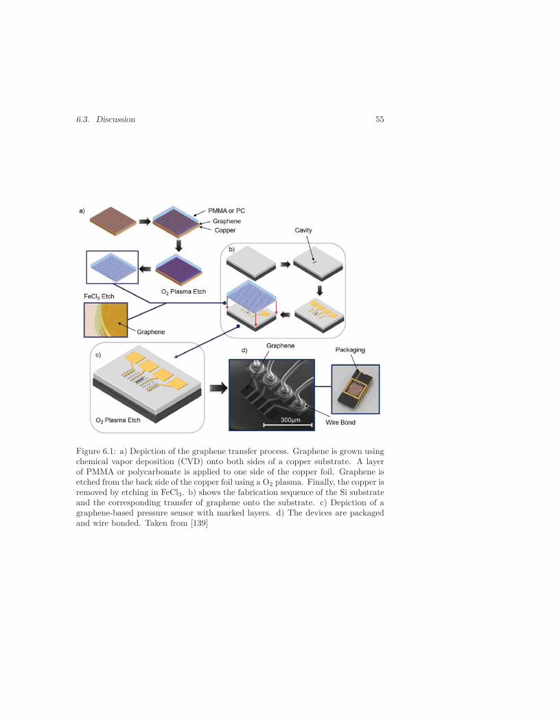
6.3. Discussion 55
Figure 6.1: a) Depiction of the graphene transfer process. Graphene is grown usingchemical vapor deposition (CVD) onto both sides of a copper substrate. A layerof PMMA or polycarbonate is applied to one side of the copper foil. Graphene isetched from the back side of the copper foil using a O2 plasma. Finally, the copper isremoved by etching in FeCl3. b) shows the fabrication sequence of the Si substrateand the corresponding transfer of graphene onto the substrate. c) Depiction of agraphene-based pressure sensor with marked layers. d) The devices are packagedand wire bonded. Taken from [139]

Chapter 7
Conclusions
Different methods for heterogeneous integration of materials into microsystems havebeen presented.
The first method, based on adhesive wafer bonding, was used for the imple-mentation of LWIR FPAs in an IC-compatible process. The second and thirdheterogeneous material integration methods presented a non-destructive way tointegrate nano-porous membranes into microfluidic components and a way totransfer massive amounts of distributed dies between different wafer formats. Bothof these methods use adhesive wafer bonding for the attachment on the targetsubstrate. The last method demonstrates how heterogeneous integration can beused to integrate a mono-layer of graphene into a pressure sensor.
The presented thesis has demonstrated that heterogeneous integration methodsare a feasible approach for integrating SiGe QW thermistor material, nano-porous membranes and graphene-layers. In common among these materials andcomponents are the specialized fabrication procedures that limits the viability ofmonolithic integration approaches. Furthermore, a blister test method to evaluateadhesive bond energies was presented.
57


Appendix A
Resistive bolometer theory
The goal of this section is to present a derivation of NETD for a resistivemicrobolometer-based camera system. Only the most important steps are derived.The interested reader is referred to [30] for details.
A.1 Optical system
Figure A.1 depicts the optical system from the viewed object to the infrared sensor.The radiant flux on the entrance pupil from the small area dA1 is given by [30]:
Φ1 = dA1πLobjectsin(β1)2 (A.1)
Likewise, the projected radiant flux on the small sensor area A2 is given by:
Φ2 = dA2πLlenssin(β2)2 (A.2)
The total radiant flux on both sides of an optical system without losses are equal,Φ1 = Φ2. The optical system is governed by Abbe’s sine law (Eq. A.3):
Object
Lens
system
Sensor
array
β1
β2
R r
h
A1
A2
Figure A.1: Depiction of the optical system. Radiation path from object to sensor.
59
60 Appendix A. Resistive bolometer theory
Table A.1: Microbolometer parameters
Parameter Unit Description
T CR %K
Temperature coefficient of resistanceβ - Bolometer fill factorα - Relative infrared absorbtion coefficientR0 Ω Resistance of microbolometer at refer-
ence temperatureIbias A Biasing currentG W
KThermal conductance
C JK
Thermal mass of microbolometerω rad · s−1 Modulation frequencyτ = C
Gs Thermal time constant
νR V Total noise voltage˜νnR
V√Hz
Normalized total noise voltageApixel m2 Pixel areaF# - Optics F-number.τopt - Relative transmission of the IR opticsε - EmissivityL W
sr · m2 RadianceΦ W Radiant fluxM W
m2 Radiant exitanceE W
m2 Irradiance
dA2sin(β2)2 = dA1sin(β1)2 (A.3)
Equation A.1 to A.3 results in that the radiance, L, is equal on both sides of theoptical system:
Lobject = Llens (A.4)
The meaning of this result is that the irradiance impinging of the sensor is governedby the radiance Lobject of the object and the parameters of the optical system. Thedistance between the object and camera system is of no importance. The radianceof the object is in turn coupled to the temperature dependent blackbody radiantexitance, εM , where ε is the emissivity. The irradiance, E, is defined as the radiantflux divided by the sensor area and is given in Equation A.6.
Lobject =εM
π(A.5)
E =Φ2dA2
= εMsin(β2)2 (A.6)
The f-number, F#, is defined as r/h (see Figure A.1). We also know that
A.1. Optical system 61
sin(β2)2 =h2
4h2
4 + r2=
14F#
2 + 1(A.7)
Assume that the transmission of the optical system is τopt. Equation A.6 forthe irradiance together with Equation A.7 for an optical system with the opticaltransmission τopt is then:
E =τoptεM
4F#2 + 1
(A.8)
A.1.1 Resistive microbolometer analysis
The responsivity is given by Equation A.9 where ΔV is the voltage response for theexchanged radiant flux ΔΦ, which is the incoming radiant flux minus the outgoingradiant flux at a reference temperature.
�V =ΔV
ΔΦ(A.9)
The absorption coefficient α is the amount of the irradiance between the wave-lengths λ1 to λ2 that is picked up by the small sensor element. The sensor elementarea βApixel then absorbs (using Equation A.8):
Φpixel =βApixel
4F#2 + 1
∫ λ2
λ1
τoptαεMλdλ (A.10)
where the radiant exitance, M , has been replaced with the spectral radiant exitanceMλ. Of interest is the sensor voltage response, �T , for changes in the viewed objecttemperature T . This is given by:
ΔV = ΔΦ�V (A.11)ΔΦ = Φpixel − Φref (A.12)
�T =∂ΔV
∂T=
βApixel�V
4F#2 + 1
∫ λ2
λ1
τoptαε∂Mλ
∂Tdλ (A.13)
NETD is defined as the object temperature difference that results in a voltageresponse equal to the voltage noise level. It is described mathematically by usingEquation A.13:
NETD =νR
�T=
νR(4F#2 + 1)
βApixel�V
1∫ λ2λ1
τoptαε ∂Mλ
∂T dλ(A.14)
while the noise equivalent power NEP and the specific detectivity D∗ is given by
62 Appendix A. Resistive bolometer theory
NEP =νR
�V(A.15)
D∗ =√
Apixel
˜νnR�V (A.16)
where ˜νnR is the total noise voltage, normalized with regards to the systembandwidth.
A.2 Thermal microbolometer model
The microbolometer temperature response due to irradiation is given by thedifferential equation:
Cth∂ΔT
∂t= ΔΦabs − GthΔT (A.17)
where ΔΦabs is the radiant flux that the sensor absorbs. Equation A.17 has thefollowing solution in the frequency domain (assuming harmonic excitation by theradiant flux ΔΦabsejωt):
ΔT (ω) =ΔΦabs
Gth
11 + jωτ
(A.18)
τ =Cth
Gth(A.19)
|ΔT (ω)| =ΔΦabs
Gth
1√1 + ω2τ2
(A.20)
where the thermal time constant τ is introduced. The temperature response ismodulated by the frequency of the irradiation and behaves like a thermal low passfilter of the impinging irradiance on the sensor. The responsivity is defined as thevoltage response relative to the irradiance and is given by Equation A.9. The signalresponse ΔV is a function of TCR, the bolometer resistance R0, the biasing currentIbias and the temperature deviation from the reference temperature ΔT .
ΔV = TCR R0 Ibias ΔT (A.21)
The following expression for �V results by combining Equation A.9, A.20 and A.21.
�V =TCR R0 Ibias
Gth
√1 + ω2τ2
(A.22)
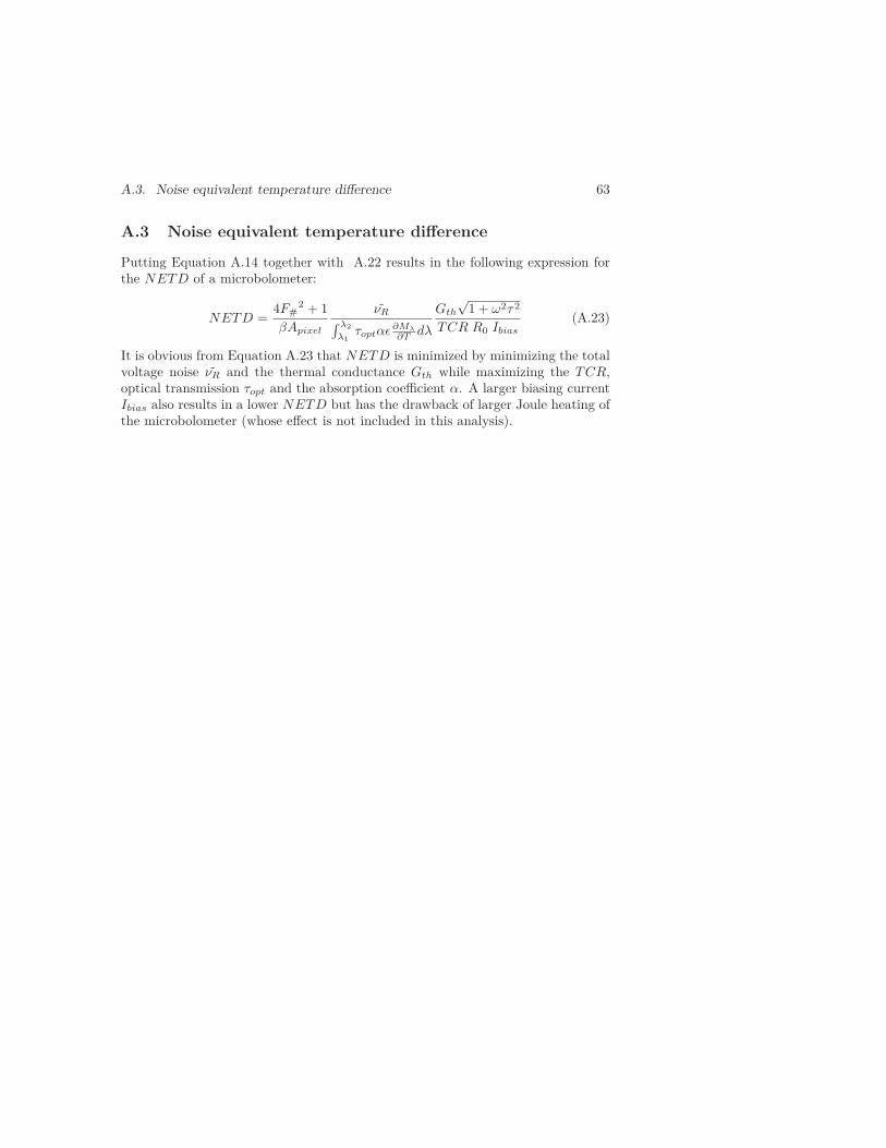
A.3. Noise equivalent temperature difference 63
A.3 Noise equivalent temperature difference
Putting Equation A.14 together with A.22 results in the following expression forthe NETD of a microbolometer:
NETD =4F#
2 + 1βApixel
νR∫ λ2λ1
τoptαε ∂Mλ
∂T dλ
Gth
√1 + ω2τ2
TCR R0 Ibias(A.23)
It is obvious from Equation A.23 that NETD is minimized by minimizing the totalvoltage noise νR and the thermal conductance Gth while maximizing the TCR,optical transmission τopt and the absorption coefficient α. A larger biasing currentIbias also results in a lower NETD but has the drawback of larger Joule heating ofthe microbolometer (whose effect is not included in this analysis).

Summary of Appended Papers
Paper 1: Heterogeneous 3D integration of 17 μm pitch Si/SiGe quantum wellbolometer arrays for infrared imaging systems
This paper reports on the realization of 17 μm × 17 μm pitch bolometer arraysfor uncooled infrared imagers. Microbolometer arrays are typically based ondeposited thin films on top of CMOS wafers that are surface-machined intosensor pixels. This paper instead focuses on the heterogeneous integration ofmonocrystalline Si/SiGe quantum-well-based thermistor material in a CMOS-compliant process using adhesive wafer bonding. The high-quality monocrys-talline thermistor material opens up for potentially lower noise comparedto commercially available uncooled microbolometer arrays together with acompetitive temperature coefficient of resistance (TCR). Complications in thefabrication of stress-free bolometer legs and low-noise contacts are discussedand analyzed.
Paper 2: Very large scale heterogeneous integration (VLSHI) and wafer-levelvacuum packaging for infrared bolometer focal plane arrays
This paper demonstrates new and improved fabrication and packagingtechnologies for next-generation IR imaging detectors based on uncooledIR bolometer focal plane arrays. The proposed technologies include verylarge scale heterogeneous integration for combining high-performance, SiGequantum-well bolometers with electronic integrated read-out circuits andCMOS compatible wafer-level vacuum packing. The fabrication and charac-terization of bolometers with a pitch of 25 μm × 25 μm that are arranged onread-out-wafers in arrays with 320 × 240 pixels are presented. The proposedCMOS compatible wafer-level vacuum packaging technology uses Cu-Sn solid-liquid interdiffusion bonding. The presented technologies are suitable forimplementation in cost-efficient fabless business models with the potential tobring about the cost reduction needed to enable low-cost IR imaging productsfor industrial, security and automotive applications.
65
66 Summary of Appended Papers
Paper 3: Wafer bonding with nano-imprint resists as sacrificial adhesive forfabrication of silicon-on-integrated-circuit (SOIC) wafers in 3D integrationof MEMS and ICs
In this paper, we present the use of thermosetting nano-imprint resistsin adhesive wafer bonding. Detailed adhesive bonding process parametersare presented to achieve void-free, well-defined and uniform wafer bondinginterfaces. Experiments have been performed to optimize the thicknesscontrol and uniformity of the nano-imprint resist layer in between the bondedwafers. In contrast to established polymer adhesives such as, e.g., BCB, nano-imprint resists as adhesives for wafer-to-wafer bonding are specifically suitableif the adhesive is intended as sacrificial material. This is often the case, e.g.,in fabrication of silicon-on-integrated-circuit(SOIC) wafers for 3D integrationof MEMS membrane structures on top of IC wafers.
Paper 4: A comparative study of the bonding energy in adhesive wafer bonding
Adhesion energies are determined for three different polymers currentlyused in adhesive wafer bonding of silicon wafers. The adhesion energies ofthe polymer off-stoichiometry thiol-ene-epoxy OSTE+ and the nano-imprintresist mr-I 9150XP are determined. The results are compared to the adhesionenergies of wafers bonded with benzocyclobutene, both with and withoutadhesion promoter. The adhesion energies of the bonds are studied by blistertests, consisting of delaminating silicon lids bonded to silicon dies with etchedcircular cavities. The critical pressure needed for delamination is convertedinto an estimate of the bond adhesion energy. The fabrication of test dies andthe evaluation method are described in detail.
Paper 5: Dry adhesive bonding of nanoporous inorganic membranes to microflu-idic devices using the OSTE(+) dual-cure polymer
Two transfer bonding schemes are presented for the incorporation of fragilenanoporous inorganic membranes into microdevices. Both schemes rely ona novel dual-cure dry adhesive bonding method, enabled by a new polymerformulation: OSTE+, which can form bonds at room temperature. OSTE+is a novel dual-cure ternary monomer system containing epoxy. After the firstcure, the OSTE+ is soft and suitable for bonding, while during the secondcure it stiffens and obtains a Young’s modulus of 1.2 GPa. The ability of theepoxy to react with almost any dry surface provides a very versatile fabricationmethod. We demonstrate the transfer bonding of porous silicon and porousalumina membranes to polymeric microfluidic chips molded into OSTE+, andof porous alumina membranes to microstructured silicon wafers, by using theOSTE+ as a thin bonding layer. The device fabrication is described andthe bond strength and membrane flow properties after bonding are evaluatedtogether with a presentation of the OSTE+ dual cure mechanism.
67
Paper 6: Batch Transfer of Radially Expanded Die Arrays for HeterogeneousIntegration Using Different Wafer Sizes
This paper reports on the realization of a novel method for batch transfer ofmultiple separate dies from a smaller substrate onto a larger wafer substrateby using a standard matrix expander in combination with an elastic dicingtape and adhesive wafer bonding. We demonstrate the expansion and transferof about 30 000 dies from a 100-mm wafer format to a 200-mm wafer.Furthermore, multiple expansions of 100-mm wafers diced into 60 000 dies areevaluated to determine the position accuracy between different expansions.Fabrication, evaluation method, and results are presented.
Paper 7: Electromechanical Piezoresistive Sensing in Suspended Graphene Mem-branes
Monolayer graphene exhibits exceptional electronic and mechanical proper-ties, making it a very promising material for nanoelectromechanical devices.The piezoresistive effect in graphene in a nanoelectromechanical membraneconfiguration is presented. This provides direct electrical readout of pressureto strain transduction. The device properties are compared with simulationsand previously reported gauge factors and simulation values. The membranein our experiment acts as a strain gauge independent of crystallographicorientation and allows for aggressive size scalability. When compared withconventional pressure sensors, the sensors have orders of magnitude highersensitivity per unit area.


Acknowledgments
First and foremost I would like to thank Professor Frank Niklaus for giving me theopportunity and resources to accomplish this Work. His moral support was and ismore than I can ask for. A special mention of Assistant Professor Niclas Roxhed isrequired. It’s fascinating to work with someone with such high calibre traits.
Umer Shah, Farizah Saharil, Henrik Gradin, Mikael Antelius, Martin Lapisa,Andreas Fischer, Mikael Sterner, Fritzi Topfer, Kristinn Gylfason, ValentinDubois and Simon Bleiker are colleagues that I foremost consider friends. Ialso acknowledge and thank everyone else at MST from Professor Goran Stemmeand down through the hierarchy. Helena Stromberg, Olof Oberg, ChristianRidder, Magnus Lindberg and Henry Radamson are colleagues in Electrumlab.I appreciated your help.
69

References
[1] R. Bogue, “Recent developments in MEMS sensors: a review of applications,markets and technologies,” Sensor Review, vol. 33, no. 4, pp. 300–304, 2013.
[2] D. K. Shaeffer, “MEMS inertial sensors: A tutorial overview,”Communications Magazine, IEEE, vol. 51, no. 4, pp. 100–109, Apr.2013. [Online]. Available: http://dx.doi.org/10.1109/mcom.2013.6495768
[3] C. Auth, “22-nm fully-depleted tri-gate CMOS transistors,” in CustomIntegrated Circuits Conference (CICC), 2012 IEEE. IEEE, 2012, pp. 1–6.[Online]. Available: http://dx.doi.org/10.1109/cicc.2012.6330657
[4] M. J. Madou, Fundamentals of Microfabrication and Nanotechnology, ThirdEdition, Three-Volume Set, 3rd ed. CRC Press, Aug. 2011. [Online].Available: http://www.worldcat.org/isbn/0849331803
[5] J. D. Plummer, M. Deal, and P. D. Griffin, Silicon VLSI Technology:Fundamentals, Practice, and Modeling, 1st ed. Prentice Hall, Jul. 2000.[Online]. Available: http://www.worldcat.org/isbn/0130850373
[6] A. C. Fischer, “Integration and Fabrication Techniques for 3D Micro-and Nanodevices,” Ph.D. dissertation, KTH Royal Institute of Technology,Department of Micro- and Nanosystems, Jan. 2013.
[7] G. K. Fedder, R. T. Howe, T.-J. K. Liu, and E. P. Quevy,“Technologies for Cofabricating MEMS and Electronics,” Proceedings ofthe IEEE, vol. 96, no. 2, pp. 306–322, Feb. 2008. [Online]. Available:http://dx.doi.org/10.1109/jproc.2007.911064
[8] S. Armbruster, F. Schafer, G. Lammel, H. Artmann, C. Schelling,H. Benzel, S. Finkbeiner, F. Larmer, R. Ruther, and O. Paul, “Anovel micromachining process for the fabrication of monocrystallineSi-membranes using porous silicon,” in TRANSDUCERS, Solid-StateSensors, Actuators and Microsystems, 12th International Conference on,2003, vol. 1. IEEE, Jun. 2003, pp. 246–249 vol.1. [Online]. Available:http://dx.doi.org/10.1109/sensor.2003.1215299
71
72 References
[9] K. Knese, S. Armbruster, H. Weber, M. Fischer, H. Benzel, M. Metz,and H. Seidel, “Novel Technology for Capacitive Pressure Sensors withMonocrystalline Silicon Membranes,” in Micro Electro Mechanical Systems,2009. MEMS 2009. IEEE 22nd International Conference on. IEEE, Jan.2009, pp. 697–700. [Online]. Available: http://dx.doi.org/10.1109/memsys.2009.4805478
[10] SiTime’s MEMS FirstT M Process, SiTime Corporation, Feb. 2009.
[11] B. S. Davis, T. Denison, and J. Kuang, “A monolithic high-g SOI-MEMSaccelerometer for measuring projectile launch and flight accelerations,” Shockand Vibration, vol. 13, no. 2, pp. 127–135, Jan. 2006. [Online]. Available:http://iospress.metapress.com/content/BHV7VDJ2BG5JM6PA
[12] T. J. Brosnihan, J. M. Bustillo, A. P. Pisano, and R. T. Howe,“Embedded interconnect and electrical isolation for high-aspect-ratio,SOI inertial instruments,” in Solid State Sensors and Actuators,1997. TRANSDUCERS ’97 Chicago., 1997 International Conferenceon, vol. 1. IEEE, Jun. 1997, pp. 637–640 vol.1. [Online]. Available:http://dx.doi.org/10.1109/sensor.1997.613732
[13] J. H. Smith, S. Montague, J. J. Sniegowski, J. R. Murray, andP. J. McWhorter, “Embedded micromechanical devices for the monolithicintegration of MEMS with CMOS,” in Electron Devices Meeting, 1995. IEDM’95., International. IEEE, Dec. 1995, pp. 609–612. [Online]. Available:http://dx.doi.org/10.1109/iedm.1995.499295
[14] J. A. Yasaitis, M. Judy, T. Brosnihan, P. M. Garone, N. Pokrovskiy,D. Sniderman, S. Limb, R. T. Howe, B. E. Boser, M. Palaniapan, X. Jiang,and S. Bhave, “A modular process for integrating thick polysilicon MEMSdevices with sub-micron CMOS,” in Proc. SPIE 4979, Micromachining andMicrofabrication Process Technology VIII, vol. 4979, 2003, pp. 145–154.[Online]. Available: http://dx.doi.org/10.1117/12.478294
[15] J. J. Neumann and K. J. Gabriel, “A fully-integrated CMOS-MEMSaudio microphone,” in TRANSDUCERS, Solid-State Sensors, Actuators andMicrosystems, 12th International Conference on, 2003, vol. 1. IEEE, Jun.2003, pp. 230–233 vol.1. [Online]. Available: http://dx.doi.org/10.1109/sensor.2003.1215295
[16] A. E. Franke, J. M. Heck, T.-J. King, and R. T. Howe,“Polycrystalline silicon-germanium films for integrated microsystems,”Journal of Microelectromechanical Systems, vol. 12, no. 2, pp. 160–171, Apr.2003. [Online]. Available: http://dx.doi.org/10.1109/jmems.2002.805051
[17] E. P. Quevy, A. San Paulo, E. Basol, R. T. Howe, T.-J. King,and J. Bokor, “Back-End-Of-Line Poly-Sige Disk Resonators,” in Micro
References 73
Electro Mechanical Systems, 2006. MEMS 2006 Istanbul. 19th IEEEInternational Conference on. IEEE, 2006, pp. 234–237. [Online]. Available:http://dx.doi.org/10.1109/memsys.2006.1627779
[18] A. Witvrouw, A. Mehta, A. Verbist, B. Du Bois, S. Van Aerde,J. Ramos-Martos, J. Ceballos, A. Ragel, J. M. Mora, M. A. Lagos, A. Arias,J. M. Hinoiosa, J. Spengler, C. Leinenbach, T. Fuchs, and S. Kronmuller,“Processing of MEMS gyroscopes on top of CMOS ICs,” in Solid-StateCircuits Conference, 2005. Digest of Technical Papers. ISSCC. 2005 IEEEInternational. IEEE, Feb. 2005, pp. 88–89 Vol. 1. [Online]. Available:http://dx.doi.org/10.1109/isscc.2005.1493882
[19] F. Niklaus, C. Vieider, and H. Jakobsen, “MEMS-based uncooled infraredbolometer arrays: a review,” in Proceedings of SPIE, ser. Society ofPhoto-Optical Instrumentation Engineers (SPIE) Conference Series, vol.6836, no. 1. SPIE, Nov. 2007, pp. 68 360D–68 360D–15. [Online]. Available:http://dx.doi.org/10.1117/12.755128
[20] CMEMS Oscillator Architecture, Silicon Laboratories Inc, 2013.
[21] E. P. Quevy, “IC-compatible MEMS structure,” Silicon Laboratories, Tech.Rep. U.S. Patent 7,514,760, Apr. 2009.
[22] M.-A. Eyoum and T.-J. King, “Low-Resistance Silicon-Germanium ContactTechnology for Modular Integration of MEMS with Electronics,” Journalof The Electrochemical Society, vol. 151, no. 3, pp. J21–J25, Mar. 2004.[Online]. Available: http://dx.doi.org/10.1149/1.1644143
[23] H. Gradin, S. Braun, G. Stemme, and W. van der Wijngaart, “SMAMicrovalves for Very Large Gas Flow Control Manufactured UsingWafer-Level Eutectic Bonding,” Industrial Electronics, IEEE Transactionson, vol. 59, no. 12, pp. 4895–4906, Dec. 2012. [Online]. Available:http://dx.doi.org/10.1109/tie.2011.2173892
[24] F. Assaderaghi, M. Daneman, and M. Lim, “NF-Shuttle: Standardizing thefabless MEMS Industry,” InvenSense Inc., Tech. Rep., 2012.
[25] A. Roer, A. Lapadatu, E. Wolla, and G. Kittilsland, “High-performanceLWIR microbolometer with Si/SiGe quantum well thermistor and waferlevel packaging,” in Proc. SPIE 8185, Electro-Optical and Infrared Systems:Technology and Applications VIII, vol. 8704, 2013, pp. 87 041B–87 041B–9.[Online]. Available: http://dx.doi.org/10.1117/12.2014914
[26] F. Forsberg, A. C. Fischer, N. Roxhed, B. Samel, P. Ericsson, G. Stemme,and F. Niklaus, “Heterogeneous 3D integration of 17 μm pitch Si/SiGequantum well bolometer arrays for infrared imaging systems,” Journal ofMicromechanics and Microengineering, vol. 23, no. 4, pp. 045 017+, Apr.2013. [Online]. Available: http://dx.doi.org/10.1088/0960-1317/23/4/045017
74 References
[27] M. Lapisa, F. Zimmer, G. Stemme, A. Gehner, and F. Niklaus,“Drift-Free Micromirror Arrays Made of Monocrystalline Silicon forAdaptive Optics Applications,” Journal of Microelectromechanical Systems,vol. 21, no. 4, pp. 959–970, Aug. 2012. [Online]. Available: http://dx.doi.org/10.1109/jmems.2012.2190713
[28] ——, “Heterogeneous 3D integration of hidden hinge micromirrorarrays consisting of two layers of monocrystalline silicon,” Journal ofMicromechanics and Microengineering, vol. 23, no. 7, pp. 075 003+, Jul.2013. [Online]. Available: http://dx.doi.org/10.1088/0960-1317/23/7/075003
[29] H. Kaplan, Practical Applications of Infrared Thermal Sensing and ImagingEquipment, Third Edition (SPIE Tutorial Text Vol. TT75) (Tutorial Textsin Optical Engineering), 3rd ed. SPIE Publications, Mar. 2007. [Online].Available: http://www.worldcat.org/isbn/0819467235
[30] H. Budzier and G. Gerlach, Thermal Infrared Sensors: Theory,Optimisation and Practice, 1st ed. Wiley, Feb. 2011. [Online]. Available:http://www.worldcat.org/isbn/047087192X
[31] A. J. Holden, “Pyroelectric sensor arrays for detection and thermalimaging,” in Proc. SPIE 8704, Infrared Technology and ApplicationsXXXIX, vol. 8704, 2013, pp. 87 041N–87 041N–10. [Online]. Available:http://dx.doi.org/10.1117/12.2014239
[32] C. M. Hanson, H. R. Beratan, and J. F. Belcher, “Uncooled infraredimaging using thin film ferroelectrics,” in Proc. SPIE 4288, Photodetectors:Materials and Devices VI, vol. 4288, 2001, pp. 298–303. [Online]. Available:http://dx.doi.org/10.1117/12.429417
[33] C. M. Hanson, H. R. Beratan, J. F. Belcher, K. R. Udayakumar, and K. L.Soch, “Advances in monolithic ferroelectric uncooled IRFPA technology,” inProc. SPIE 3379, Infrared Detectors and Focal Plane Arrays V, vol. 3379,1998, pp. 60–68. [Online]. Available: http://dx.doi.org/10.1117/12.317622
[34] A. Graf, M. Arndt, M. Sauer, and G. Gerlach, “Review of micromachinedthermopiles for infrared detection,” Measurement Science and Technology,vol. 18, no. 7, pp. R59+, Jul. 2007. [Online]. Available: http://dx.doi.org/10.1088/0957-0233/18/7/r01
[35] M. Hirota, Y. Nakajima, M. Saito, F. Satou, and M. Uchiyama, “120×90element thermopile array fabricated with CMOS technology,” in Proc. SPIE4820, Infrared Technology and Applications XXVIII, vol. 4820, 2003, pp.239–249. [Online]. Available: http://dx.doi.org/10.1117/12.457719
[36] U. Mizrahi, N. Argaman, S. Elkind, A. Giladi, Y. Hirsh, M. Labilov,I. Pivnik, N. Shiloah, M. Singer, A. Tuito, M. Ben-Ezra, and
References 75
I. Shtrichman, “Large-format 17 μm high-end VOx μ-bolometer infrareddetector,” in Proc. SPIE 8704, Infrared Technology and ApplicationsXXXIX, vol. 8704, 2013, pp. 87 041H–87 041H–8. [Online]. Available:http://dx.doi.org/10.1117/12.2015653
[37] T. Endoh, S. Tohyama, T. Yamazaki, Y. Tanaka, K. Okuyama, S. Kurashina,M. Miyoshi, K. Katoh, T. Yamamoto, Y. Okuda, T. Sasaki, H. Ishizaki,T. Nakajima, K. Shinoda, and T. Tsuchiya, “Uncooled infrared detectorwith 12μm pixel pitch video graphics array,” in Proc. SPIE 8704, InfraredTechnology and Applications XXXIX, vol. 8704, 2013, pp. 87 041G–87 041G–11. [Online]. Available: http://dx.doi.org/10.1117/12.2013690
[38] M. Kohin and N. R. Butler, “Performance limits of uncooledVOx microbolometer focal plane arrays,” in Society of Photo-OpticalInstrumentation Engineers (SPIE) Conference Series, ser. Society ofPhoto-Optical Instrumentation Engineers (SPIE) Conference Series, B. F.Andresen and G. F. Fulop, Eds., vol. 5406, Aug. 2004, pp. 447–453. [Online].Available: http://dx.doi.org/10.1117/12.542482
[39] C. Li, G. D. Skidmore, C. Howard, C. J. Han, L. Wood, D. Peysha,E. Williams, C. Trujillo, J. Emmett, G. Robas, D. Jardine, C. F. Wan,and E. Clarke, “Recent development of ultra small pixel uncooled focalplane arrays at DRS,” in Society of Photo-Optical Instrumentation Engineers(SPIE) Conference Series, ser. Society of Photo-Optical InstrumentationEngineers (SPIE) Conference Series, vol. 6542, May 2007. [Online]. Available:http://dx.doi.org/10.1117/12.720267
[40] C. Trouilleau, B. Fieque, J. L. Tissot, P. Robert, A. Crastes, C. Minassian,O. Legras, B. Dupont, A. Touvignon, S. Tinnes, J. J. Yon, and A. Arnaud,“Uncooled amorphous silicon 160 x 120 irfpa with 25-μm pixel-pitch for largevolume applications,” in Society of Photo-Optical Instrumentation Engineers(SPIE) Conference Series, ser. Society of Photo-Optical InstrumentationEngineers (SPIE) Conference Series, vol. 6542, May 2007. [Online]. Available:http://dx.doi.org/10.1117/12.723599
[41] D. Murphy, M. Ray, J. Wyles, C. Hewitt, R. Wyles, E. Gordon, K. Almada,T. Sessler, S. Baur, D. V. Lue, and S. Black, “640 × 512 17 μmmicrobolometer fpa and sensor development,” in Society of Photo-OpticalInstrumentation Engineers (SPIE) Conference Series, ser. Society ofPhoto-Optical Instrumentation Engineers (SPIE) Conference Series, vol.6542, May 2007. [Online]. Available: http://dx.doi.org/10.1117/12.724345
[42] R. J. Blackwell, T. Bach, D. O’Donnell, J. Geneczko, and M. Joswick,“17 μm pixel 640 x 480 microbolometer fpa development at baesystems,” in Society of Photo-Optical Instrumentation Engineers (SPIE)Conference Series, ser. Society of Photo-Optical Instrumentation Engineers
76 References
(SPIE) Conference Series, vol. 6542, May 2007. [Online]. Available:http://dx.doi.org/10.1117/12.723474
[43] K. C. Liddiard, “Thin-film resistance bolometer IR detectors,” InfraredPhysics, vol. 24, no. 1, pp. 57–64, Jan. 1984. [Online]. Available:http://dx.doi.org/10.1016/0020-0891(84)90048-4
[44] ——, “Thin-film resistance bolometer IR detectorsâĂŤII,” InfraredPhysics, vol. 26, no. 1, pp. 43–49, Jan. 1986. [Online]. Available:http://dx.doi.org/10.1016/0020-0891(86)90046-1
[45] T. Schimert, C. Hanson, J. Brady, T. Fagan, M. Taylor, W. McCardel,R. Gooch, M. Gohlke, and A. J. Syllaios, “Advances in small-pixel, large-format Îś-Si bolometer arrays,” in Proc. SPIE 7298, Infrared Technologyand Applications XXXV, vol. 7298, 2009, pp. 72 980T–72 980T–5. [Online].Available: http://dx.doi.org/10.1117/12.818576
[46] F. Purkl, T. English, G. Yama, J. Provine, A. K. Samarao, A. Feyh,G. O’Brien, O. Ambacher, R. T. Howe, and T. W. Kenny, “Sub-10nanometer uncooled platinum bolometers via plasma enhanced atomic layerdeposition,” in Micro Electro Mechanical Systems (MEMS), 2013 IEEE26th International Conference on. IEEE, Jan. 2013, pp. 185–188. [Online].Available: http://dx.doi.org/10.1109/memsys.2013.6474208
[47] K. Yamashita, A. Murata, and M. Okuyama, “Miniaturized infrared sensorusing silicon diaphragm based on Golay cell,” Sensors and ActuatorsA: Physical, vol. 66, no. 1-3, pp. 29–32, Apr. 1998. [Online]. Available:http://dx.doi.org/10.1016/s0924-4247(97)01702-0
[48] R. B. Erarslan, S. Z. Lulec, U. Adiyan, S. Olcer, Y. Temiz, Y. Leblebici,H. Torun, and H. Urey, “MEMS sensor array platform integrated with CMOSbased optical readout,” in Micro Electro Mechanical Systems (MEMS), 2013IEEE 26th International Conference on. IEEE, Jan. 2013, pp. 181–184.[Online]. Available: http://dx.doi.org/10.1109/memsys.2013.6474207
[49] J. P. Salerno, “High frame rate imaging using uncooled optical readoutphotomechanical IR sensor,” in Proc. SPIE 6542, Infrared Technology andApplications XXXIII, vol. 6542, 2007, pp. 65 421D–65 421D–9. [Online].Available: http://dx.doi.org/10.1117/12.718785
[50] I. Ishikawa, M. Ueno, K. Endo, Y. Nakaki, H. Hata, T. Sone, and M. Kimata,“Low-cost 320x240 uncooled IRFPA using conventional silicon IC process,”Opto-electronics Review, vol. 7, no. 4, pp. 297–303, 1999.
[51] D. Takamuro, T. Maegawa, T. Sugino, Y. Kosasayama, T. Ohnakado,H. Hata, M. Ueno, H. Fukumoto, K. Ishida, H. Katayama, T. Imai,and M. Ueno, “Development of new SOI diode structure for beyond
References 77
17 μm pixel pitch SOI diode uncooled IRFPAs,” in Society ofPhoto-Optical Instrumentation Engineers (SPIE) Conference Series, ser.Society of Photo-Optical Instrumentation Engineers (SPIE) ConferenceSeries, vol. 8012, May 2011, pp. 80 121E–80 121E–10. [Online]. Available:http://dx.doi.org/10.1117/12.884556
[52] I. Fujiwara, K. Sasaki, K. Suzuki, H. Yagi, H. Kwon, H. Honda, K. Ishii,M. Ogata, M. Atsuta, R. Ueno, M. Kobayashi, and H. Funaki, “Scale down ofp-n junction diodes of an uncooled ir-fpa for improvement of the sensitivityand thermal time response by 0.13-μm cmos technology,” in Society of Photo-Optical Instrumentation Engineers (SPIE) Conference Series, ser. Societyof Photo-Optical Instrumentation Engineers (SPIE) Conference Series, vol.8012, May 2011. [Online]. Available: http://dx.doi.org/10.1117/12.883342
[53] M. Ueno, Y. Kosasayama, T. Sugino, Y. Nakaki, Y. Fujii, H. Inoue,K. Kama, T. Seto, M. Takeda, and M. Kimata, “640 x 480 pixel uncooledinfrared FPA with SOI diode detectors,” in Society of Photo-OpticalInstrumentation Engineers (SPIE) Conference Series, ser. Society ofPhoto-Optical Instrumentation Engineers (SPIE) Conference Series, B. F.Andresen and G. F. Fulop, Eds., vol. 5783, May 2005, pp. 566–577. [Online].Available: http://dx.doi.org/10.1117/12.609665
[54] D. Fujisawa, T. Maegawa, Y. Ohta, Y. Kosasayama, T. Ohnakado,H. Hata, M. Ueno, H. Ohji, R. Sato, H. Katayama, T. Imai, andM. Ueno, “Two-million-pixel SOI diode uncooled IRFPA with 15μmpixel pitch,” in Proc. SPIE 8353, Infrared Technology and ApplicationsXXXVIII, vol. 8353, 2012, pp. 83 531G–83 531G–13. [Online]. Available:http://dx.doi.org/10.1117/12.919520
[55] P. W. Kruse, Uncooled Thermal Imaging Arrays, Systems, and Applications(SPIE Tutorial Texts in Optical Engineering Vol. TT51). SPIE Publications,Jul. 2001. [Online]. Available: http://www.worldcat.org/isbn/0819441228
[56] ——, “Can the 300-K radiating background noise limit be attained byuncooled thermal imagers?” in Society of Photo-Optical InstrumentationEngineers (SPIE) Conference Series, ser. Society of Photo-OpticalInstrumentation Engineers (SPIE) Conference Series, vol. 5406, Aug. 2004,pp. 437–446. [Online]. Available: http://dx.doi.org/10.1117/12.539388
[57] K. C. Liddiard, “Application of interferometric enhancement to self-absorbingthin film thermal IR detectors,” Infrared Physics, vol. 34, no. 4, pp. 379–387,Aug. 1993. [Online]. Available: http://dx.doi.org/10.1016/0020-0891(93)90070-n
[58] S. E. Kucuk, M. Yusuf Tanrikulu, and T. Akin, “A detailed analysis for theabsorption coefficient of multilevel uncooled infrared detectors,” in Proc. SPIE
78 References
8012, Infrared Technology and Applications XXXVII, vol. 8012, 2011, pp.80 121R–80 121R–8. [Online]. Available: http://dx.doi.org/10.1117/12.890236
[59] F. Niklaus, A. Decharat, C. Jansson, and G. Stemme, “Performancemodel for uncooled infrared bolometer arrays and performance predictionsof bolometers operating at atmospheric pressure,” Infrared Physics &Technology, vol. 51, no. 3, pp. 168–177, Jan. 2008. [Online]. Available:http://dx.doi.org/10.1016/j.infrared.2007.08.001
[60] P. Eriksson, J. Y. Andersson, and G. Stemme, “Thermal characterizationof surface-micromachined silicon nitride membranes for thermal infrareddetectors,” Journal of Microelectromechanical Systems, vol. 6, no. 1, pp.55–61, Mar. 1997. [Online]. Available: http://dx.doi.org/10.1109/84.557531
[61] M. Haartman and M. Ostling, Low-Frequency Noise in Advanced MOSDevices (Analog Circuits and Signal Processing), 2007th ed. Springer, Jul.2007. [Online]. Available: http://www.worldcat.org/isbn/9781402059100
[62] F. N. Hooge, “1/f noise sources,” Electron Devices, IEEE Transactionson, vol. 41, no. 11, pp. 1926–1935, Nov. 1994. [Online]. Available:http://dx.doi.org/10.1109/16.333808
[63] L. K. J. Vandamme and F. N. Hooge, “What do we certainly knowabout 1/f noise in mosts?” Electron Devices, IEEE Transactionson, vol. 55, no. 11, pp. 3070–3085, Nov. 2008. [Online]. Available:http://dx.doi.org/10.1109/ted.2008.2005167
[64] H. H. Radamson, M. Kolahdouz, S. Shayestehaminzadeh, A. A. Farniya, andS. Wissmar, “Carbon-doped single-crystalline SiGe/Si thermistor with hightemperature coefficient of resistance and low noise level,” Applied PhysicsLetters, vol. 97, no. 22, pp. 223 507–223 507–2, Nov. 2010. [Online]. Available:http://dx.doi.org/10.1063/1.3524211
[65] C. Li, C. J. Han, G. D. Skidmore, G. Cook, K. Kubala, R. Bates, D. Temple,J. Lannon, A. Hilton, K. Glukh, and B. Hardy, “Low-cost uncooled VOxinfrared camera development,” in Proc. SPIE 8704, Infrared Technologyand Applications XXXIX, vol. 8704, 2013, pp. 87 041L–87 041L–10. [Online].Available: http://dx.doi.org/10.1117/12.2019653
[66] J. L. Tissot, S. Tinnes, A. Durand, C. Minassian, P. Robert, and M. Vilain,“High-performance uncooled amorphous silicon VGA and XGA IRFPA with17μm pixel-pitch,” in Proc. SPIE 7834, Electro-Optical and Infrared Systems:Technology and Applications VII, vol. 7834, 2010, pp. 78 340K–78 340K–8.[Online]. Available: http://dx.doi.org/10.1117/12.864867
[67] A. Tanaka, S. Matsumoto, N. Tsukamoto, S. Itoh, K. Chiba, T. Endoh,A. Nakazato, K. Okuyama, Y. Kumazawa, M. Hijikawa, H. Gotoh,
References 79
T. Tanaka, and N. Teranishi, “Infrared focal plane array incorporatingsilicon IC process compatible bolometer,” Electron Devices, IEEETransactions on, vol. 43, no. 11, pp. 1844–1850, Nov. 1996. [Online].Available: http://dx.doi.org/10.1109/16.543017
[68] H. A. Basantani, H.-B. Shin, T. N. Jackson, and M. W. Horn,“Vertically integrated pixel microbolometers for IR imaging using high-resistivity VOx,” in Proc. SPIE 8704, Infrared Technology and ApplicationsXXXIX, vol. 8704, 2013, pp. 87 041A–87 041A–5. [Online]. Available:http://dx.doi.org/10.1117/12.2016292
[69] T. Ishikawa, M. Ueno, Y. Nakaki, K. Endo, Y. Ohta, J. Nakanishi,Y. Kosasayama, H. Yagi, T. Sone, and M. Kimata, “Performance of 320x 240 uncooled IRFPA with SOI diode detectors,” in Proc. SPIE 4130,Infrared Technology and Applications XXVI, vol. 4130, 2000, pp. 152–159.[Online]. Available: http://dx.doi.org/10.1117/12.409857
[70] S. Wissmar, L. Hoglund, J. Andersson, C. Vieider, S. Savage, andP. Ericsson, “High signal-to-noise ratio quantum well bolometer materials,”in Society of Photo-Optical Instrumentation Engineers (SPIE) ConferenceSeries, ser. Society of Photo-Optical Instrumentation Engineers (SPIE)Conference Series, vol. 6401, no. 1. The International Society for OpticalEngineering., Oct. 2006, pp. 64 010N–64 010N–11. [Online]. Available:http://dx.doi.org/10.1117/12.689874
[71] F. Forsberg, N. Roxhed, A. C. Fischer, B. Samel, P. Ericsson, N. Hoivik,A. Lapadatu, M. Bring, G. Kittilsland, G. Stemme, and F. Niklaus,“Very large scale heterogeneous integration (VLSHI) and wafer-level vacuumpackaging for infrared bolometer focal plane arrays,” Infrared Physics& Technology, vol. 60, pp. 251–259, Sep. 2013. [Online]. Available:http://dx.doi.org/10.1016/j.infrared.2013.05.006
[72] A. C. Fischer, M. Lapisa, N. Roxhed, G. Stemme, and F. Niklaus, “Selectiveelectroless nickel plating on oxygen-plasma-activated gold seed-layers forthe fabrication of low contact resistance vias and microstructures,” inMicro Electro Mechanical Systems (MEMS), 2010 IEEE 23rd InternationalConference on. IEEE, Jan. 2010, pp. 472–475. [Online]. Available:http://dx.doi.org/10.1109/memsys.2010.5442462
[73] P. Neuzil and T. Mei, “Evaluation of thermal parameters of bolometerdevices,” Applied Physics Letters, vol. 80, no. 10, pp. 1838–1840, 2002.[Online]. Available: http://dx.doi.org/10.1063/1.1458686
[74] X. Gu, G. Karunasiri, G. Chen, U. Sridhar, and B. Xu, “Determinationof thermal parameters of microbolometers using a single electricalmeasurement,” Applied Physics Letters, vol. 72, no. 15, pp. 1881–1883, Apr.1998. [Online]. Available: http://dx.doi.org/10.1063/1.121214
80 References
[75] F. Niklaus, P. Ericsson, M. Bring, D. Eriksson, T. Krekels, and H. Ottevaere,“Infrared Imaging Components for Use in Automotive Safety Applications- Deliverable D1.3A,” Seventh Framework Programme (FP7) - EuropeanUnion, Tech. Rep., Sep. 2011.
[76] F. Niklaus, G. Stemme, Lu, and R. J. Gutmann, “Adhesive wafer bonding,”Journal of Applied Physics, vol. 99, no. 3, pp. 031 101–031 101–28, Feb. 2006.[Online]. Available: http://dx.doi.org/10.1063/1.2168512
[77] A. Bayrashev and B. Ziaie, “Silicon wafer bonding through RF dielectricheating,” Sensors and Actuators A: Physical, vol. 103, no. 1-2, pp. 16–22, Jan.2003. [Online]. Available: http://dx.doi.org/10.1016/s0924-4247(02)00327-8
[78] F. Niklaus, P. Enoksson, E. Kalvesten, and G. Stemme, “Low-temperature full wafer adhesive bonding,” Journal of Micromechanics andMicroengineering, vol. 11, no. 2, pp. 100+, Mar. 2001. [Online]. Available:http://dx.doi.org/10.1088/0960-1317/11/2/303
[79] W. H. Teh, G. Lihui, R. Kumar, and D. L. Kwong, “200-mm wafer-scaletransfer of 0.18-μm dual-damascene Cu/SiO/sub2/interconnection system toplastic substrates,” IEEE Electron Device Letters, vol. 26, no. 11, pp. 802–804,Nov. 2005. [Online]. Available: http://dx.doi.org/10.1109/led.2005.857734
[80] J. W. Kwon, S. Kamal-Bahl, and E. S. Kim, “Film transfer and bondingtechnique to cover lab on a chip,” in The 13th International Conference onSolid-State Sensors, Actuators and Microsystems, 2005. Digest of TechnicalPapers. TRANSDUCERS ’05. IEEE, 2005, pp. 940–943. [Online]. Available:http://dx.doi.org/10.1109/sensor.2005.1496573
[81] M. Antelius, “Wafer-scale Vacuum and Liquid Packaging Concepts for anOptical Thin-film Gas Sensor,” Ph.D. dissertation, KTH Royal Institute ofTechnology, Stockholm, Sweden, Apr. 2013.
[82] T. Ohba, N. Maeda, H. Kitada, K. Fujimoto, K. Suzuki, T. Nakamura,A. Kawai, and K. Arai, “Thinned wafer multi-stack 3DI technology,”Microelectronic Engineering, vol. 87, no. 3, pp. 485–490, Mar. 2010. [Online].Available: http://dx.doi.org/10.1016/j.mee.2009.07.006
[83] Y. Kwon, J. Seok, J.-Q. Lu, T. S. Cale, and R. J. Gutmann, “CriticalAdhesion Energy of Benzocyclobutene-Bonded Wafers,” Journal of TheElectrochemical Society, vol. 153, no. 4, pp. G347–G352, Apr. 2006. [Online].Available: http://dx.doi.org/10.1149/1.2172551
[84] ——, “Critical Adhesion Energy at the Interface Between Benzocyclobuteneand Silicon Nitride Layers,” Journal of The Electrochemical Society,vol. 154, no. 6, pp. H460–H465, Jun. 2007. [Online]. Available:http://dx.doi.org/10.1149/1.2717504
References 81
[85] G. Roelkens, J. Van Campenhout, J. Brouckaert, D. Van Thourhout,R. Baets, P. R. Romeo, P. Regreny, A. Kazmierczak, C. Seassal,X. Letartre, G. Hollinger, J. M. Fedeli, L. Di Cioccio, and C. Lagahe-Blanchard, “III-V/Si photonics by die-to-wafer bonding,” MaterialsToday, vol. 10, no. 7-8, pp. 36–43, Jul. 2007. [Online]. Available:http://dx.doi.org/10.1016/s1369-7021(07)70178-5
[86] A. Jourdain, P. De Moor, K. Baert, I. De Wolf, and H. A. C.Tilmans, “Mechanical and electrical characterization of BCB as a bondand seal material for cavities housing (RF-)MEMS devices,” Journal ofMicromechanics and Microengineering, vol. 15, no. 7, pp. S89+, Jul. 2005.[Online]. Available: http://dx.doi.org/10.1088/0960-1317/15/7/013
[87] F. J. Blanco, M. Agirregabiria, J. Garcia, J. Berganzo, M. Tijero,M. T. Arroyo, J. M. Ruano, I. Aramburu, and K. Mayora, “Novelthree-dimensional embedded SU-8 microchannels fabricated using a lowtemperature full wafer adhesive bonding,” Journal of Micromechanics andMicroengineering, vol. 14, no. 7, pp. 1047–1056, Jul. 2004. [Online]. Available:http://dx.doi.org/10.1088/0960-1317/14/7/027
[88] C. T. Pan, H. Yang, S. C. Shen, M. C. Chou, and H. P. Chou, “A low-temperature wafer bonding technique using patternable materials,” Journalof Micromechanics and Microengineering, vol. 12, no. 5, pp. 611–615, Sep.2002. [Online]. Available: http://dx.doi.org/10.1088/0960-1317/12/5/315
[89] S. Li, C. B. Freidhoff, R. M. Young, and R. Ghodssi, “Fabrication ofmicronozzles using low-temperature wafer-level bonding with SU-8,” Journalof Micromechanics and Microengineering, vol. 13, no. 5, pp. 732+, Sep. 2003.[Online]. Available: http://dx.doi.org/10.1088/0960-1317/13/5/328
[90] R. J. Jackman, T. M. Floyd, R. Ghodssi, M. A. Schmidt, and K. F.Jensen, “Microfluidic systems with on-line UV detection fabricated inphotodefinable epoxy,” Journal of Micromechanics and Microengineering,vol. 11, no. 3, pp. 263–269, May 2001. [Online]. Available: http://dx.doi.org/10.1088/0960-1317/11/3/316
[91] L. Yu, F. E. H. Tay, G. Xu, B. Chen, M. Avram, and C. Iliescu, “Adhesivebonding with SU-8 at wafer level for microfluidic devices,” Journal ofPhysics: Conference Series, vol. 34, no. 1, pp. 776+, Apr. 2006. [Online].Available: http://dx.doi.org/10.1088/1742-6596/34/1/128
[92] P. Salvo, R. Verplancke, F. Bossuyt, D. Latta, B. Vandecasteele,C. Liu, and J. Vanfleteren, “Adhesive bonding by SU-8 transferfor assembling microfluidic devices,” Microfluidics and Nanofluidics,vol. 13, no. 6, pp. 987–991, Jun. 2012. [Online]. Available: http://dx.doi.org/10.1007/s10404-012-1011-x
82 References
[93] F. Niklaus, A. Decharat, F. Forsberg, N. Roxhed, M. Lapisa, M. Populin,F. Zimmer, J. Lemm, and G. Stemme, “Wafer bonding with nano-imprintresists as sacrificial adhesive for fabrication of silicon-on-integrated-circuit(SOIC) wafers in 3D integration of MEMS and ICs,” Sensors and ActuatorsA: Physical, vol. 154, no. 1, pp. 180–186, Aug. 2009. [Online]. Available:http://dx.doi.org/10.1016/j.sna.2009.07.009
[94] S. J. Bennett, K. L. Devries, and M. L. Williams, “Adhesive fracturemechanics,” International Journal of Fracture, vol. 10, no. 1, pp. 33–43,1974. [Online]. Available: http://dx.doi.org/10.1007/bf00955077
[95] F. Forsberg, F. Saharil, T. Haraldsson, N. Roxhed, G. Stemme,W. van der Wijngaart, and F. Niklaus, “A comparative study of thebonding energy in adhesive wafer bonding,” Journal of Micromechanicsand Microengineering, vol. 23, no. 8, pp. 085 019+, Aug. 2013. [Online].Available: http://dx.doi.org/10.1088/0960-1317/23/8/085019
[96] C. C. Striemer, T. R. Gaborski, J. L. McGrath, and P. M. Fauchet,“Charge- and size-based separation of macromolecules using ultrathin siliconmembranes,” Nature, vol. 445, no. 7129, pp. 749–753, Feb. 2007. [Online].Available: http://dx.doi.org/10.1038/nature05532
[97] H. Masuda, H. Yamada, M. Satoh, H. Asoh, M. Nakao, and T. Tamamura,“Highly ordered nanochannel-array architecture in anodic alumina,” AppliedPhysics Letters, vol. 71, no. 19, pp. 2770–2772, Nov. 1997. [Online].Available: http://dx.doi.org/10.1063/1.120128
[98] M. G. Elgort, M. G. Herrmann, M. Erali, J. D. Durtschi, K. V. Voelkerding,and R. E. Smith, “Extraction and Amplification of Genomic DNA fromHuman Blood on Nanoporous Aluminum Oxide Membranes,” ClinicalChemistry, vol. 50, no. 10, pp. 1817–1819, Oct. 2004. [Online]. Available:http://dx.doi.org/10.1373/clinchem.2004.035162
[99] G. Sigalov, J. Comer, G. Timp, and A. Aksimentiev, “Detection of DNASequences Using an Alternating Electric Field in a Nanopore Capacitor,”Nano Lett., vol. 8, no. 1, pp. 56–63, Dec. 2007. [Online]. Available:http://dx.doi.org/10.1021/nl071890k
[100] E. Anglin, L. Cheng, W. Freeman, and M. Sailor, “Porous siliconin drug delivery devices and materials,” Advanced Drug DeliveryReviews, vol. 60, no. 11, pp. 1266–1277, Aug. 2008. [Online]. Available:http://dx.doi.org/10.1016/j.addr.2008.03.017
[101] V. S. Y. Lin, K. Motesharei, K.-P. S. Dancil, M. J. Sailor, andM. R. Ghadiri, “A Porous Silicon-Based Optical Interferometric Biosensor,”Science, vol. 278, no. 5339, pp. 840–843, Oct. 1997. [Online]. Available:http://dx.doi.org/10.1126/science.278.5339.840
References 83
[102] S. D. Alvarez, C.-P. Li, C. E. Chiang, I. K. Schuller, and M. J.Sailor, “A Label-Free Porous Alumina Interferometric Immunosensor,” ACSNano, vol. 3, no. 10, pp. 3301–3307, Aug. 2009. [Online]. Available:http://dx.doi.org/10.1021/nn900825q
[103] R. W. Tjerkstra, G. E. Gardeniers, J. J. Kelly, and A. van den Berg,“Multi-walled microchannels: free-standing porous silicon membranes foruse in μTAS,” Journal of Microelectromechanical Systems, vol. 9, no. 4, pp.495–501, Dec. 2000. [Online]. Available: http://dx.doi.org/10.1109/84.896771
[104] D. J. Gargas, O. Muresan, D. J. Sirbuly, and S. K. Buratto, “MicropatternedPorous-Silicon Bragg Mirrors by Dry-Removal Soft Lithography,” Adv.Mater., vol. 18, no. 23, pp. 3164–3168, 2006. [Online]. Available:http://dx.doi.org/10.1002/adma.200601354
[105] G. Rong, J. D. Ryckman, R. L. Mernaugh, and S. M. Weiss, “Label-free porous silicon membrane waveguide for DNA sensing,” AppliedPhysics Letters, vol. 93, no. 16, pp. 161 109+, 2008. [Online]. Available:http://dx.doi.org/10.1063/1.3005620
[106] A. Carlson, A. M. Bowen, Y. Huang, R. G. Nuzzo, and J. A. Rogers,“Transfer Printing Techniques for Materials Assembly and Micro/NanodeviceFabrication,” Adv. Mater., vol. 24, no. 39, pp. 5284–5318, 2012. [Online].Available: http://dx.doi.org/10.1002/adma.201201386
[107] N. Xu, Y. Lin, S. A. Hofstadler, D. Matson, C. J. Call, and R. D. Smith,“A Microfabricated Dialysis Device for Sample Cleanup in ElectrosprayIonization Mass Spectrometry,” Anal. Chem., vol. 70, no. 17, pp. 3553–3556,Aug. 1998. [Online]. Available: http://dx.doi.org/10.1021/ac980233x
[108] F. Xiang, Y. Lin, J. Wen, D. W. Matson, and R. D. Smith, “An IntegratedMicrofabricated Device for Dual Microdialysis and On-Line ESI-Ion TrapMass Spectrometry for Analysis of Complex Biological Samples,” Anal.Chem., vol. 71, no. 8, pp. 1485–1490, Mar. 1999. [Online]. Available:http://dx.doi.org/10.1021/ac981400w
[109] F. Saharil, F. Forsberg, Y. Liu, P. Bettotti, N. Kumar, F. Niklaus,T. Haraldsson, W. van der Wijngaart, and K. B. Gylfason, “Dryadhesive bonding of nanoporous inorganic membranes to microfluidic devicesusing the OSTE(+) dual-cure polymer,” Journal of Micromechanics andMicroengineering, vol. 23, no. 2, pp. 025 021+, Jan. 2013. [Online]. Available:http://dx.doi.org/10.1088/0960-1317/23/2/025021
[110] F. Forsberg, N. Roxhed, T. Haraldsson, Y. Liu, G. Stemme, and F. Niklaus,“Batch Transfer of Radially Expanded Die Arrays for HeterogeneousIntegration Using Different Wafer Sizes,” Journal of Microelectromechanical
84 References
Systems, vol. 21, no. 5, pp. 1077–1083, Oct. 2012. [Online]. Available:http://dx.doi.org/10.1109/jmems.2012.2203105
[111] G. Roelkens, J. Brouckaert, D. Van Thourhout, R. Baets, R. Notzel,and M. Smit, “Adhesive Bonding of InP/InGaAsP Dies to ProcessedSilicon-On-Insulator Wafers using DVS-bis-Benzocyclobutene,” Journal ofThe Electrochemical Society, vol. 153, no. 12, pp. G1015–G1019, Dec. 2006.[Online]. Available: http://dx.doi.org/10.1149/1.2352045
[112] S. Stankovic, R. Jones, J. Heck, M. Sysak, D. Van Thourhout, andG. Roelkens, “Die-to-Die Adhesive Bonding Procedure for Evanescently-Coupled Photonic Devices,” Electrochemical and Solid-State Letters,vol. 14, no. 8, pp. H326–H329, Aug. 2011. [Online]. Available: http://dx.doi.org/10.1149/1.3592267
[113] J. Brouckaert, G. Roelkens, D. Van Thourhout, and R. Baets, “CompactInAlAs-InGaAs Metal-Semiconductor-Metal Photodetectors Integrated onSilicon-on-Insulator Waveguides,” Photonics Technology Letters, IEEE,vol. 19, no. 19, pp. 1484–1486, Oct. 2007. [Online]. Available: http://dx.doi.org/10.1109/lpt.2007.903767
[114] S. Farrens, “Wafer and die bonding technologies for 3D integration,” in MRSFall 2008 Proceedings E. Proc. MRS Fall Meeting, 2008.
[115] 3800 Die Bonder datasheet, Palomar Technologies, Carlsbad, 2011.
[116] ESEC 2008 HS Plus Data Sheet, BE Semiconductor Industries, 2012.
[117] M. Mastrangeli, S. Abbasi, C. Varel, C. Van Hoof, J. P. Celis, andK. F. Bohringer, “Self-assembly from milli- to nanoscales: methodsand applications,” Journal of Micromechanics and Microengineering,vol. 19, no. 8, pp. 083 001+, Aug. 2009. [Online]. Available: http://dx.doi.org/10.1088/0960-1317/19/8/083001
[118] H. O. Jacobs, A. R. Tao, A. Schwartz, D. H. Gracias, and G. M.Whitesides, “Fabrication of a Cylindrical Display by Patterned Assembly,”Science, vol. 296, no. 5566, pp. 323–325, Apr. 2002. [Online]. Available:http://dx.doi.org/10.1126/science.1069153
[119] W. Zheng and H. . O. Jacobs, “Self-Assembly Process to Integrate andConnect Semiconductor Dies on Surfaces with Single-Angular Orientationand Contact-Pad Registration,” Adv. Mater., vol. 18, no. 11, pp. 1387–1392,Jun. 2006. [Online]. Available: http://dx.doi.org/10.1002/adma.200502026
[120] H. J. Yeh and J. S. Smith, “Fluidic self-assembly for the integrationof GaAs light-emitting diodes on Si substrates,” Photonics TechnologyLetters, IEEE, vol. 6, no. 6, pp. 706–708, Jun. 1994. [Online]. Available:http://dx.doi.org/10.1109/68.300169
References 85
[121] J. Fang and K. F. Bohringer, “Parallel micro component-to-substrateassembly with controlled poses and high surface coverage,” Journal ofMicromechanics and Microengineering, vol. 16, no. 4, pp. 721+, Apr. 2006.[Online]. Available: http://dx.doi.org/10.1088/0960-1317/16/4/008
[122] S. A. Stauth and B. A. Parviz, “Self-assembled single-crystal siliconcircuits on plastic,” Proceedings of the National Academy of Sciences,vol. 103, no. 38, pp. 13 922–13 927, Sep. 2006. [Online]. Available:http://dx.doi.org/10.1073/pnas.0602893103
[123] A. C. Fischer, S. J. Bleiker, T. Haraldsson, N. Roxhed, G. Stemme,and F. Niklaus, “Very high aspect ratio through-silicon vias (TSVs)fabricated using automated magnetic assembly of nickel wires,” Journalof Micromechanics and Microengineering, vol. 22, no. 10, pp. 105 001+,Oct. 2012. [Online]. Available: http://dx.doi.org/10.1088/0960-1317/22/10/105001
[124] C. F. Edman, R. B. Swint, C. Gurtner, R. E. Formosa, S. D. Roh, K. E.Lee, P. D. Swanson, D. E. Ackley, J. J. Coleman, and M. J. Heller, “Electricfield directed assembly of an InGaAs LED onto silicon circuitry,” PhotonicsTechnology Letters, IEEE, vol. 12, no. 9, pp. 1198–1200, Sep. 2000. [Online].Available: http://dx.doi.org/10.1109/68.874234
[125] Q. Ramadan, Y. S. Uk, and K. Vaidyanathan, “Large scale microcomponentsassembly using an external magnetic array,” Applied Physics Letters,vol. 90, no. 17, pp. 172 502–172 502–3, Apr. 2007. [Online]. Available:http://dx.doi.org/10.1063/1.2731708
[126] K. Huang, R. Dinyari, G. Lanzara, J. Y. Kim, J. Feng, C. Vancura,F.-K. Chang, and P. Peumans, “An Approach to Cost-Effective, Robust,Large-Area Electronics using Monolithic Silicon,” in Electron DevicesMeeting, 2007. IEDM 2007. IEEE International. IEEE, Dec. 2007, pp.217–220. [Online]. Available: http://dx.doi.org/10.1109/iedm.2007.4418906
[127] H. C. Ko, M. P. Stoykovich, J. Song, V. Malyarchuk, W. M. Choi,C.-J. Yu, J. B. Geddes, J. Xiao, S. Wang, Y. Huang, and J. A. Rogers,“A hemispherical electronic eye camera based on compressible siliconoptoelectronics,” Nature, vol. 454, no. 7205, pp. 748–753, Aug. 2008.[Online]. Available: http://dx.doi.org/10.1038/nature07113
[128] W. P. Eaton and J. H. Smith, “Micromachined pressure sensors: review andrecent developments,” Smart Materials and Structures, vol. 6, no. 5, pp. 530+,Oct. 1997. [Online]. Available: http://dx.doi.org/10.1088/0964-1726/6/5/004
[129] A. K. Geim and K. S. Novoselov, “The rise of graphene,” NatureMaterials, vol. 6, no. 3, pp. 183–191, Mar. 2007. [Online]. Available:http://dx.doi.org/10.1038/nmat1849
86 References
[130] Y. Zhang, L. Zhang, and C. Zhou, “Review of Chemical Vapor Deposition ofGraphene and Related Applications,” Acc. Chem. Res., Mar. 2013. [Online].Available: http://dx.doi.org/10.1021/ar300203n
[131] K. I. Bolotin, K. J. Sikes, Z. Jiang, M. Klima, G. Fudenberg, J. Hone,P. Kim, and H. L. Stormer, “Ultrahigh electron mobility in suspendedgraphene,” Solid State Communications, vol. 146, no. 9-10, pp. 351–355,Jun. 2008. [Online]. Available: http://dx.doi.org/10.1016/j.ssc.2008.02.024
[132] S. V. Morozov, K. S. Novoselov, M. I. Katsnelson, F. Schedin, D. C. Elias,J. A. Jaszczak, and A. K. Geim, “Giant Intrinsic Carrier Mobilities inGraphene and Its Bilayer,” Phys. Rev. Lett., vol. 100, no. 1, pp. 016 602+,2008.
[133] C. Lee, X. Wei, J. W. Kysar, and J. Hone, “Measurement ofthe Elastic Properties and Intrinsic Strength of Monolayer Graphene,”Science, vol. 321, no. 5887, pp. 385–388, Jul. 2008. [Online]. Available:http://dx.doi.org/10.1126/science.1157996
[134] G.-H. Lee, R. C. Cooper, S. J. An, S. Lee, A. van der Zande, N. Petrone,A. G. Hammerberg, C. Lee, B. Crawford, W. Oliver, J. W. Kysar, andJ. Hone, “High-Strength Chemical-Vapor-Deposited Graphene and GrainBoundaries,” Science, vol. 340, no. 6136, pp. 1073–1076, May 2013. [Online].Available: http://dx.doi.org/10.1126/science.1235126
[135] H. Tomori, A. Kanda, H. Goto, Y. Ootuka, K. Tsukagoshi, S. Moriyama,E. Watanabe, and D. Tsuya, “Introducing Nonuniform Strain to GrapheneUsing Dielectric Nanopillars,” Appl. Phys. Express, vol. 4, pp. 075 102+,Jun. 2011. [Online]. Available: http://arxiv.org/abs/1106.1507
[136] S. P. Koenig, N. G. Boddeti, M. L. Dunn, and J. S. Bunch,“Ultrastrong adhesion of graphene membranes,” Nature Nanotechnology,vol. 6, no. 9, pp. 543–546, Aug. 2011. [Online]. Available: http://dx.doi.org/10.1038/nnano.2011.123
[137] J. S. Bunch, S. S. Verbridge, J. S. Alden, A. M. van der Zande, J. M. Parpia,H. G. Craighead, and P. L. McEuen, “Impermeable Atomic Membranesfrom Graphene Sheets,” Nano Lett., vol. 8, no. 8, pp. 2458–2462, Jul. 2008.[Online]. Available: http://dx.doi.org/10.1021/nl801457b
[138] V. M. Pereira, A. H. Castro Neto, and N. M. R. Peres, “Tight-bindingapproach to uniaxial strain in graphene,” Physical Review B, vol. 80, no. 4,pp. 045 401+, 2009.
[139] A. D. Smith, F. Niklaus, A. Paussa, S. Vaziri, A. C. Fischer, M. Sterner,F. Forsberg, A. Delin, D. Esseni, P. Palestri, M. Ostling, and M. C.Lemme, “Electromechanical Piezoresistive Sensing in Suspended Graphene

References 87
Membranes,” Nano Lett., vol. 13, no. 7, pp. 3237–3242, Jun. 2013. [Online].Available: http://dx.doi.org/10.1021/nl401352k


![[-0.9em]Integration and deployment of Unitex-based ...infolingu.univ-mlv.fr/slides_unitex_webservices.pdfOutline Problem Architecture Proof-of-Concept Conclusions Future Work Integration](https://static.fdocument.org/doc/165x107/600b24713f41d377bc203950/-09emintegration-and-deployment-of-unitex-based-outline-problem-architecture.jpg)