GO1555 Voltage Controlled Oscillator - Future Electronics · GO1555 Voltage Controlled Oscillator...
12
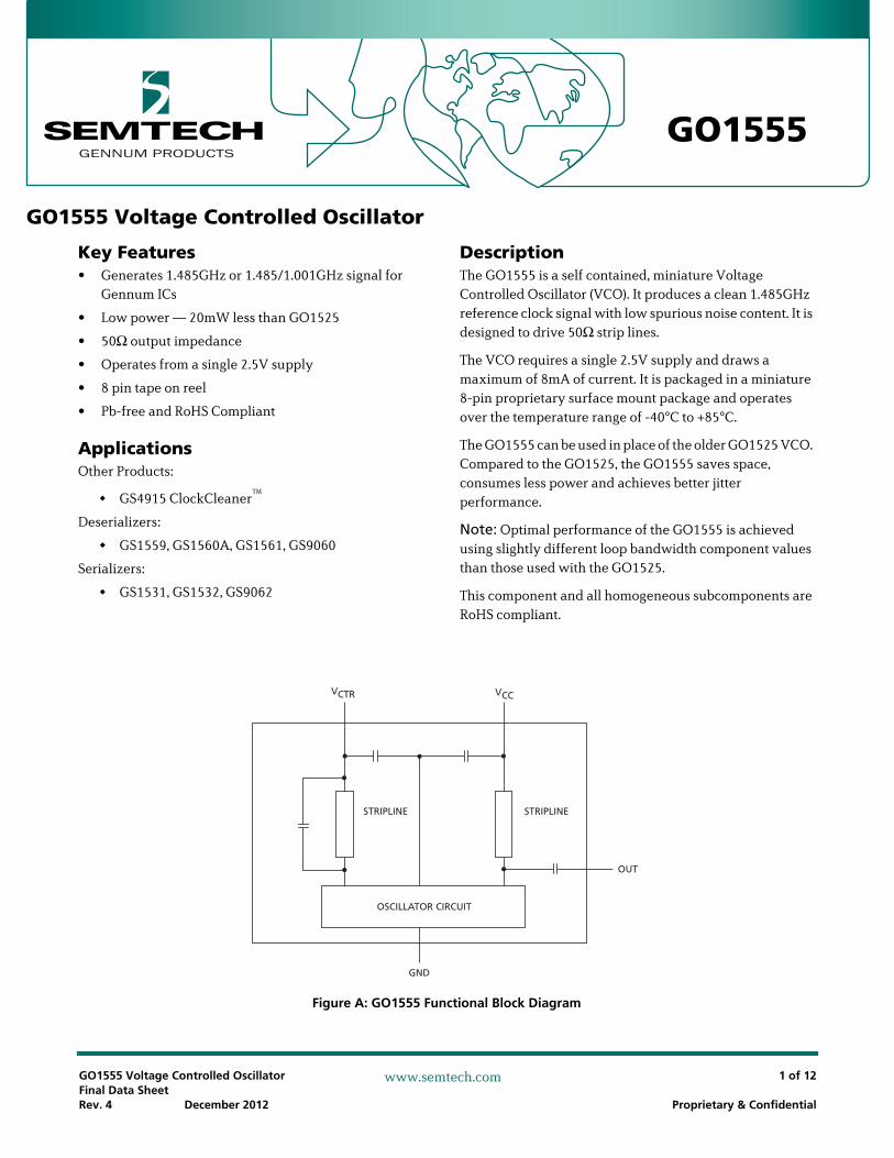
GO1555 Voltage Controlled Oscillator GO1555 1 of 12 Proprietary & Confidential GO1555 Voltage Controlled Oscillator Final Data Sheet Rev. 4 December 2012 www.semtech.com Key Features • Generates 1.485GHz or 1.485/1.001GHz signal for Gennum ICs • Low power — 20mW less than GO1525 • 50Ω output impedance • Operates from a single 2.5V supply • 8 pin tape on reel • Pb-free and RoHS Compliant Applications Other Products: GS4915 ClockCleaner ™ Deserializers: GS1559, GS1560A, GS1561, GS9060 Serializers: GS1531, GS1532, GS9062 Description The GO1555 is a self contained, miniature Voltage Controlled Oscillator (VCO). It produces a clean 1.485GHz reference clock signal with low spurious noise content. It is designed to drive 50Ω strip lines. The VCO requires a single 2.5V supply and draws a maximum of 8mA of current. It is packaged in a miniature 8-pin proprietary surface mount package and operates over the temperature range of -40°C to +85°C. The GO1555 can be used in place of the older GO1525 VCO. Compared to the GO1525, the GO1555 saves space, consumes less power and achieves better jitter performance. Note: Optimal performance of the GO1555 is achieved using slightly different loop bandwidth component values than those used with the GO1525. This component and all homogeneous subcomponents are RoHS compliant. Figure A: GO1555 Functional Block Diagram OSCILLATOR CIRCUIT STRIPLINE STRIPLINE V CTR V CC OUT GND
Transcript of GO1555 Voltage Controlled Oscillator - Future Electronics · GO1555 Voltage Controlled Oscillator...
GO1555 Voltage Controlled Oscillator
GO1555
1 of 12
Proprietary & Confidential
GO1555 Voltage Controlled OscillatorFinal Data SheetRev. 4 December 2012
www.semtech.com
Key Features• Generates 1.485GHz or 1.485/1.001GHz signal for
Gennum ICs
• Low power — 20mW less than GO1525
• 50Ω output impedance
• Operates from a single 2.5V supply
• 8 pin tape on reel
• Pb-free and RoHS Compliant
ApplicationsOther Products:
GS4915 ClockCleaner™
Deserializers:
GS1559, GS1560A, GS1561, GS9060
Serializers:
GS1531, GS1532, GS9062
DescriptionThe GO1555 is a self contained, miniature Voltage Controlled Oscillator (VCO). It produces a clean 1.485GHz reference clock signal with low spurious noise content. It is designed to drive 50Ω strip lines.
The VCO requires a single 2.5V supply and draws a maximum of 8mA of current. It is packaged in a miniature 8-pin proprietary surface mount package and operates over the temperature range of -40°C to +85°C.
The GO1555 can be used in place of the older GO1525 VCO. Compared to the GO1525, the GO1555 saves space, consumes less power and achieves better jitter performance.
Note: Optimal performance of the GO1555 is achieved using slightly different loop bandwidth component values than those used with the GO1525.
This component and all homogeneous subcomponents are RoHS compliant.
Figure A: GO1555 Functional Block Diagram
OSCILLATOR CIRCUIT
STRIPLINESTRIPLINE
VCTR VCC
OUT
GND
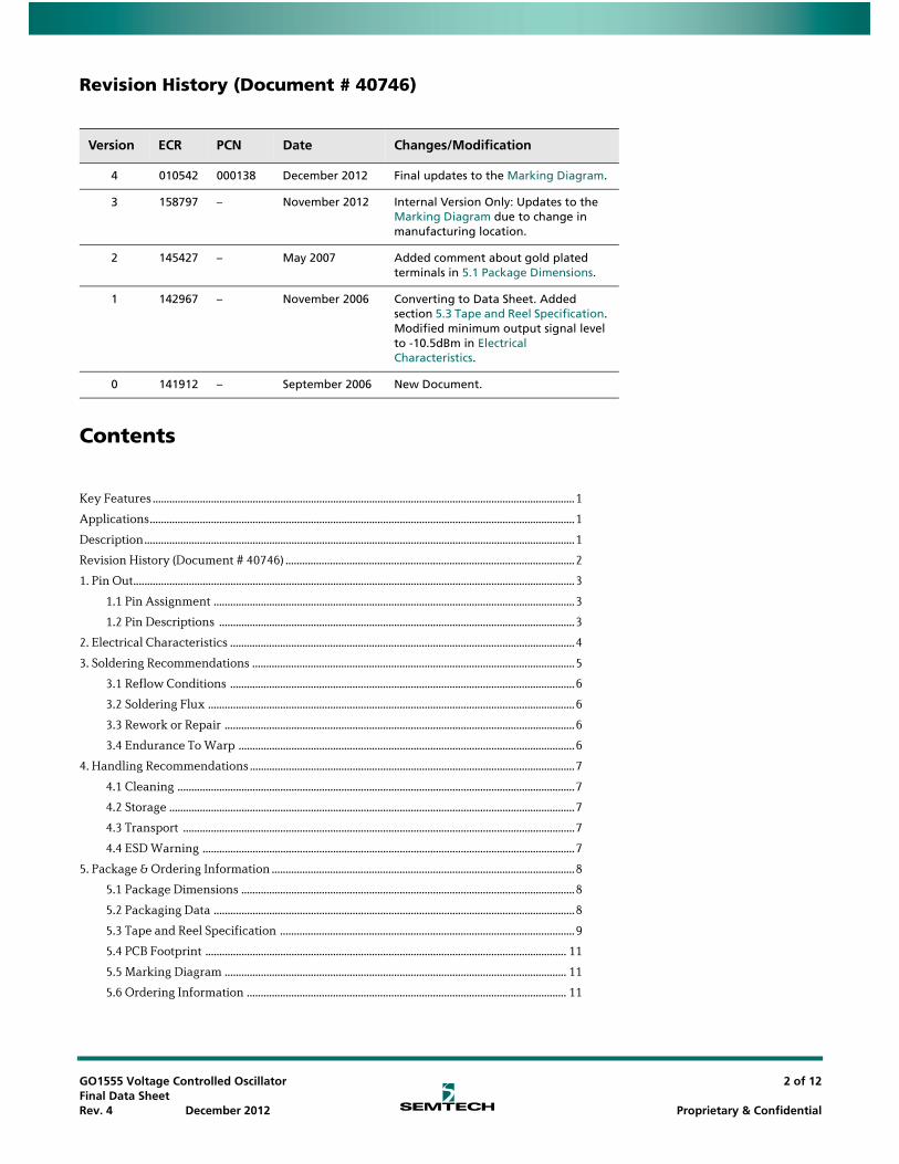
Revision History (Document # 40746)
Contents
Key Features ........................................................................................................................................................1
Applications.........................................................................................................................................................1
Description...........................................................................................................................................................1
Revision History (Document # 40746) ........................................................................................................2
1. Pin Out...............................................................................................................................................................3
1.1 Pin Assignment ..................................................................................................................................3
1.2 Pin Descriptions ................................................................................................................................3
2. Electrical Characteristics ............................................................................................................................4
3. Soldering Recommendations ....................................................................................................................5
3.1 Reflow Conditions ............................................................................................................................6
3.2 Soldering Flux ....................................................................................................................................6
3.3 Rework or Repair ..............................................................................................................................6
3.4 Endurance To Warp .........................................................................................................................6
4. Handling Recommendations .....................................................................................................................7
4.1 Cleaning ...............................................................................................................................................7
4.2 Storage ..................................................................................................................................................7
4.3 Transport .............................................................................................................................................7
4.4 ESD Warning ......................................................................................................................................7
5. Package & Ordering Information .............................................................................................................8
5.1 Package Dimensions ........................................................................................................................8
5.2 Packaging Data ..................................................................................................................................8
5.3 Tape and Reel Specification ..........................................................................................................9
5.4 PCB Footprint .................................................................................................................................. 11
5.5 Marking Diagram ........................................................................................................................... 11
5.6 Ordering Information ................................................................................................................... 11
Version ECR PCN Date Changes/Modification
4 010542 000138 December 2012 Final updates to the Marking Diagram.
3 158797 – November 2012 Internal Version Only: Updates to the Marking Diagram due to change in manufacturing location.
2 145427 – May 2007 Added comment about gold plated terminals in 5.1 Package Dimensions.
1 142967 – November 2006 Converting to Data Sheet. Added section 5.3 Tape and Reel Specification. Modified minimum output signal level to -10.5dBm in Electrical Characteristics.
0 141912 – September 2006 New Document.
GO1555 Voltage Controlled OscillatorFinal Data SheetRev. 4 December 2012
2 of 12
Proprietary & Confidential
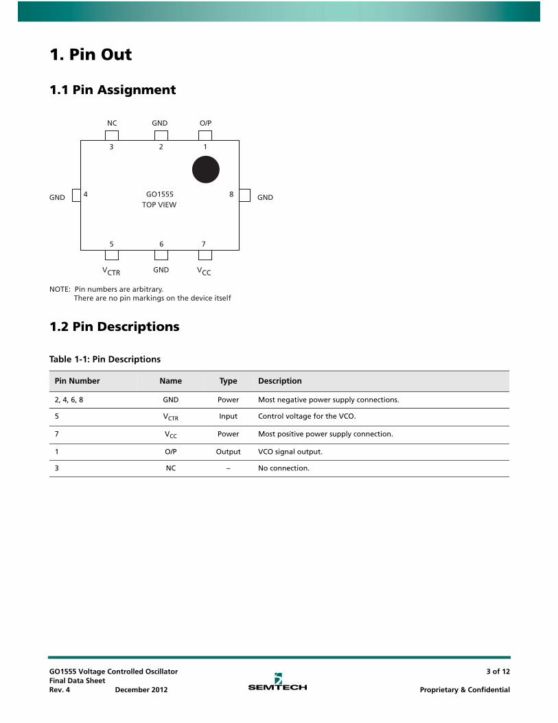
1. Pin Out
1.1 Pin Assignment
1.2 Pin Descriptions
GO1555
NC GND O/P
GNDGND
GND VCCVCTR
3 2 1
4 8
5 76
NOTE: Pin numbers are arbitrary. There are no pin markings on the device itself
TOP VIEW
Table 1-1: Pin Descriptions
Pin Number Name Type Description
2, 4, 6, 8 GND Power Most negative power supply connections.
5 VCTR Input Control voltage for the VCO.
7 VCC Power Most positive power supply connection.
1 O/P Output VCO signal output.
3 NC – No connection.
GO1555 Voltage Controlled OscillatorFinal Data SheetRev. 4 December 2012
3 of 12
Proprietary & Confidential
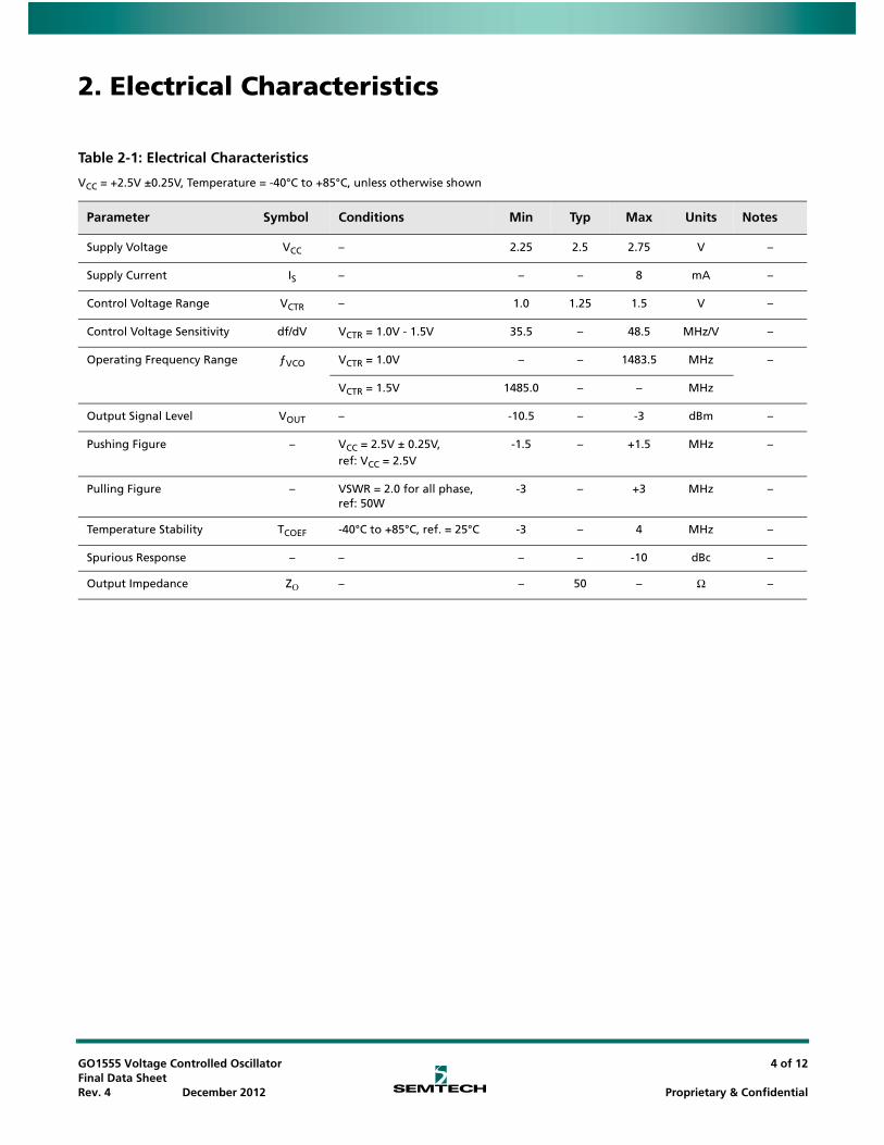
2. Electrical Characteristics
Table 2-1: Electrical Characteristics
VCC = +2.5V ±0.25V, Temperature = -40°C to +85°C, unless otherwise shown
Parameter Symbol Conditions Min Typ Max Units Notes
Supply Voltage VCC – 2.25 2.5 2.75 V –
Supply Current IS – – – 8 mA –
Control Voltage Range VCTR – 1.0 1.25 1.5 V –
Control Voltage Sensitivity df/dV VCTR = 1.0V - 1.5V 35.5 – 48.5 MHz/V –
Operating Frequency Range ƒVCO VCTR = 1.0V – – 1483.5 MHz –
VCTR = 1.5V 1485.0 – – MHz
Output Signal Level VOUT – -10.5 – -3 dBm –
Pushing Figure – VCC = 2.5V ± 0.25V, ref: VCC = 2.5V
-1.5 – +1.5 MHz –
Pulling Figure – VSWR = 2.0 for all phase, ref: 50W
-3 – +3 MHz –
Temperature Stability TCOEF -40°C to +85°C, ref. = 25°C -3 – 4 MHz –
Spurious Response – – – – -10 dBc –
Output Impedance ZO – – 50 – Ω –
GO1555 Voltage Controlled OscillatorFinal Data SheetRev. 4 December 2012
4 of 12
Proprietary & Confidential
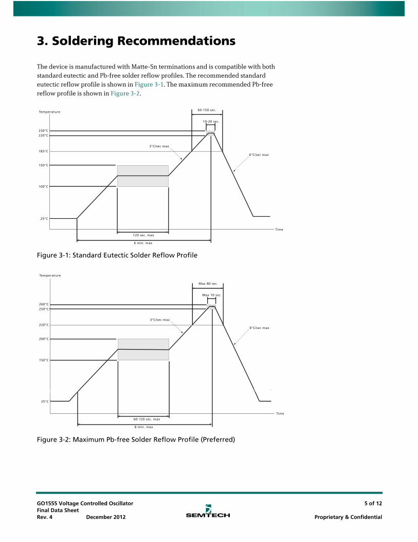
3. Soldering Recommendations
The device is manufactured with Matte-Sn terminations and is compatible with both standard eutectic and Pb-free solder reflow profiles. The recommended standard eutectic reflow profile is shown in Figure 3-1. The maximum recommended Pb-free reflow profile is shown in Figure 3-2.
Figure 3-1: Standard Eutectic Solder Reflow Profile
Figure 3-2: Maximum Pb-free Solder Reflow Profile (Preferred)
25°C
100°C
150°C
183°C
230°C220°C
Time
Temperature
6 min. max
120 sec. max
60-150 sec.
10-20 sec.
3°C/sec max
6°C/sec max
25°C
150°C
200°C
220°C
260°C250°C
Time
Temperature
8 min. max
60-120 sec. max
Max 80 sec.
Max 10 sec.
3°C/sec max
6°C/sec max
GO1555 Voltage Controlled OscillatorFinal Data SheetRev. 4 December 2012
5 of 12
Proprietary & Confidential
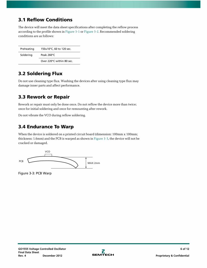
3.1 Reflow ConditionsThe device will meet the data sheet specifications after completing the reflow process according to the profile shown in Figure 3-1 or Figure 3-2. Recommended soldering conditions are as follows:
3.2 Soldering FluxDo not use cleaning type flux. Washing the devices after using cleaning type flux may damage inner parts and affect performance.
3.3 Rework or RepairRework or repair must only be done once. Do not reflow the device more than twice; once for initial soldering and once for remounting after rework.
Do not vibrate the VCO during reflow soldering.
3.4 Endurance To WarpWhen the device is soldered on a printed circuit board (dimension: 100mm x 100mm; thickness: 1.6mm) and the PCB is warped as shown in Figure 3-3, the device will not be cracked or damaged.
Figure 3-3: PCB Warp
Preheating 150±10°C, 60 to 120 sec.
Soldering Peak 260°C
Over 220°C within 80 sec.
VCO
PCBMAX 2mm
GO1555 Voltage Controlled OscillatorFinal Data SheetRev. 4 December 2012
6 of 12
Proprietary & Confidential
4. Handling Recommendations
4.1 CleaningThere are two options for cleaning the devices.
Option 1:
1. Clean but do not use solvent cleaners.
2. Thoroughly dry assemblies afterwards.
Option 2:
1. Mount device after board is cleaned.
4.2 StorageStore the devices out of direct sunlight, at a stable temperature and humidity. Avoid extreme temperatures, high humidity and wide temperature fluctuations. Condensation on the devices may result in reduced quality and lowered solderability.
Avoid dust, sea breezes and corrosive gases (Cl2, NH3, SO2, NOX, etc.).
Use within 6 months after delivery. If the devices are stored for more than one year, solderability may be degraded.
4.3 TransportPackage the devices for transportation to avoid mechanical vibration or shock.
4.4 ESD WarningAvoid poor ground connections and electrostatic discharge or induction in production.
GO1555 Voltage Controlled OscillatorFinal Data SheetRev. 4 December 2012
7 of 12
Proprietary & Confidential
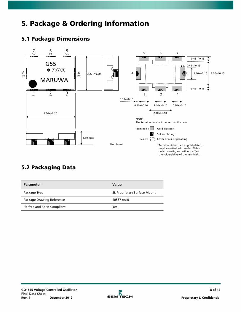
5. Package & Ordering Information
5.1 Package Dimensions
5.2 Packaging Data
4 83.20+/-0.20
4.50+/-0.20
0.45+/-0.15
0.45+/-0.15
0.45+/-0.15
1.10+/-0.10 2.30+/-0.10
765
1230.30+/-0.15
0.90+/-0.10 1.10+/-0.10 0.90+/-0.10
2.10+/-0.10
1.50 max.
Unit (mm)
NOTE:The terminals are not marked on the case.
Terminals :
Resist :
Gold plating*
Solder plating
Cover of resist spreading
*Terminals identified as gold plated, may be wetted with solder. This is only cosmetic, and will not affect the solderability of the terminals.
G55
NCGNDOUT
GNDGND
GND VCTRVCC
1 2 3
567
8 ∗ 1 2 3
MARUWA4
Parameter Value
Package Type 8L Proprietary Surface Mount
Package Drawing Reference 40567 rev.0
Pb-free and RoHS Compliant Yes
GO1555 Voltage Controlled OscillatorFinal Data SheetRev. 4 December 2012
8 of 12
Proprietary & Confidential
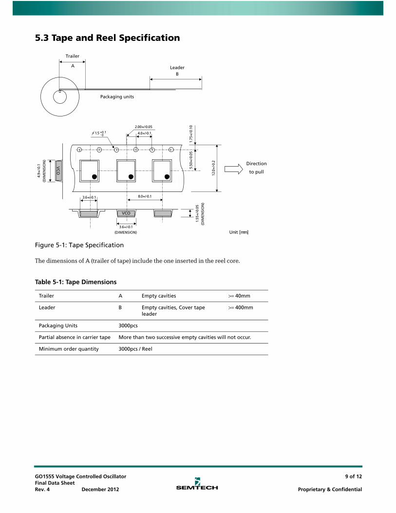
5.3 Tape and Reel Specification
Figure 5-1: Tape Specification
The dimensions of A (trailer of tape) include the one inserted in the reel core.
Table 5-1: Tape Dimensions
Trailer A Empty cavities >= 40mm
Leader B Empty cavities, Cover tape leader
>= 400mm
Packaging Units 3000pcs
Partial absence in carrier tape More than two successive empty cavities will not occur.
Minimum order quantity 3000pcs / Reel
A
B
Trailer
Leader
Packaging units
Unit [mm]
Direction
to pull
1.5 +0.1- 0
VCO
VC
O
4.0+/-0.1
2.00+/-0.05
8.0+/-0.1
3.6+/-0.1
(DIMENSION)
1.55
+/-0
.05
(DIM
ENSI
ON
)
4.9+
/-0.1
(DIM
ENSI
ON
)
1.75
+/-0
.10
5.50
+/-0
.05
12.0
+/-0
.2
3.6+/-0.1
GO1555 Voltage Controlled OscillatorFinal Data SheetRev. 4 December 2012
9 of 12
Proprietary & Confidential
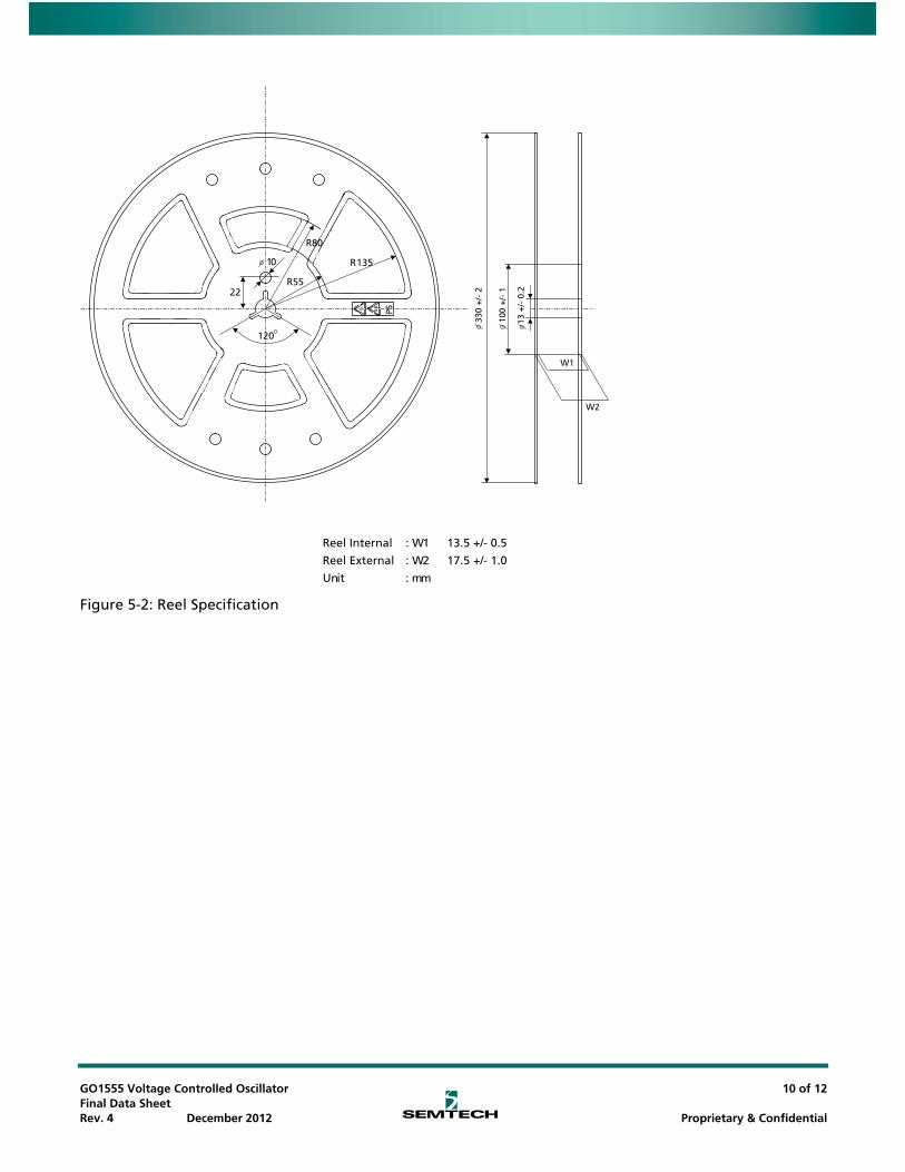
Figure 5-2: Reel Specification
Reel Internal : W1 13.5 +/- 0.5
Reel External : W2 17.5 +/- 1.0
Unit : mm
R80
R135
R5522
10
120
W1
W2
PS0.66
330
+/-
2
100
+/-
1
13
+/-
0.2
GO1555 Voltage Controlled OscillatorFinal Data SheetRev. 4 December 2012
10 of 12
Proprietary & Confidential
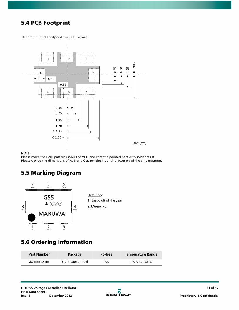
5.4 PCB Footprint
5.5 Marking Diagram
5.6 Ordering Information
Unit [mm]
1.05
0.55
0.8
0.85
0.55
1.70
A 1.9 ~
C 2.55 ~
1.05
B 1.
90 ~
0.75
0.80
123
4
765
8
Recommended Footprint for PCB Layout
NOTE:Please make the GND pattern under the VCO and coat the painted part with solder resist.Please decide the dimensions of A, B and C as per the mounting accuracy of the chip mounter.
Date Code
1 : Last digit of the year
2,3: Week No.
G55
NCGNDOUT
GNDGND
GND VCTRVCC
1 2 3
567
8 ∗ 1 2 3
MARUWA4
Part Number Package Pb-free Temperature Range
GO1555-IXTE3 8-pin tape on reel Yes -40°C to +85°C
GO1555 Voltage Controlled OscillatorFinal Data SheetRev. 4 December 2012
11 of 12
Proprietary & Confidential
© Semtech 2012
All rights reserved. Reproduction in whole or in part is prohibited without the prior written consent of the copyrightowner. The information presented in this document does not form part of any quotation or contract, is believed to beaccurate and reliable and may be changed without notice. No liability will be accepted by the publisher for anyconsequence of its use. Publication thereof does not convey nor imply any license under patent or other industrial orintellectual property rights. Semtech assumes no responsibility or liability whatsoever for any failure or unexpectedoperation resulting from misuse, neglect improper installation, repair or improper handling or unusual physical orelectrical stress including, but not limited to, exposure to parameters beyond the specified maximum ratings oroperation outside the specified range.
SEMTECH PRODUCTS ARE NOT DESIGNED, INTENDED, AUTHORIZED OR WARRANTED TO BE SUITABLE FOR USE INLIFE-SUPPORT APPLICATIONS, DEVICES OR SYSTEMS OR OTHER CRITICAL APPLICATIONS. INCLUSION OF SEMTECHPRODUCTS IN SUCH APPLICATIONS IS UNDERSTOOD TO BE UNDERTAKEN SOLELY AT THE CUSTOMER’S OWN RISK.Should a customer purchase or use Semtech products for any such unauthorized application, the customer shallindemnify and hold Semtech and its officers, employees, subsidiaries, affiliates, and distributors harmless against allclaims, costs damages and attorney fees which could arise.
Notice: All referenced brands, product names, service names and trademarks are the property of their respective owners.
DOCUMENT IDENTIFICATIONFINAL DATA SHEETInformation relating to this product and the application or design described herein is believed to be reliable, however such information is provided as a guide only and Semtech assumes no liability for any errors in this document, or for the application or design described herein. Semtech reserves the right to make changes to the product or this document at any time without notice.
Contact Information
Semtech CorporationGennum Products Division
200 Flynn Road, Camarillo, CA 93012Phone: (805) 498-2111, Fax: (805) 498-3804
www.semtech.com
CAUTIONELECTROSTATIC SENSITIVE DEVICES
DO NOT OPEN PACKAGES OR HANDLE EXCEPT AT A STATIC-FREE WORKSTATION
GO1555 Voltage Controlled OscillatorFinal Data SheetRev. 4 December 2012
12 of 1212
Proprietary & Confidential