Generation 5 eGaN® Technology A Quantum Leap into a...
19
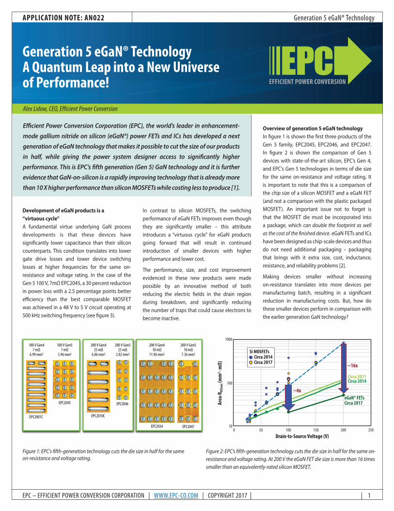
APPLICATION NOTE: AN022 EPC – EFFICIENT POWER CONVERSION CORPORATION | WWW.EPC-CO.COM | COPYRIGHT 2017 | | 1 Generation 5 eGaN® Technology Generation 5 eGaN® Technology A Quantum Leap into a New Universe of Performance! EFFICIENT POWER CONVERSION Alex Lidow, CEO, Efficient Power Conversion Efficient Power Conversion Corporation (EPC), the world’s leader in enhancement- mode gallium nitride on silicon (eGaN®) power FETs and ICs has developed a next generation of eGaN technology that makes it possible to cut the size of our products in half, while giving the power system designer access to significantly higher performance. This is EPC’s fifth generation (Gen 5) GaN technology and it is further evidence that GaN-on-silicon is a rapidly improving technology that is already more than 10 X higher performance than silicon MOSFETs while costing less to produce [1]. Development of eGaN products is a “virtuous cycle” A fundamental virtue underlying GaN process developments is that these devices have significantly lower capacitance than their silicon counterparts. This condition translates into lower gate drive losses and lower device switching losses at higher frequencies for the same on- resistance and voltage rating. In the case of the Gen 5 100 V, 7mΩ EPC2045, a 30 percent reduction in power loss with a 2.5 percentage points better efficiency than the best comparable MOSFET was achieved in a 48 V to 5 V circuit operating at 500 kHz switching frequency (see figure 3). In contrast to silicon MOSFETs, the switching performance of eGaN FETs improves even though they are significantly smaller – this attribute introduces a “virtuous cycle” for eGaN products going forward that will result in continued introduction of smaller devices with higher performance and lower cost. The performance, size, and cost improvement evidenced in these new products were made possible by an innovative method of both reducing the electric fields in the drain region during breakdown, and significantly reducing the number of traps that could cause electrons to become inactive. Overview of generation 5 eGaN technology In figure 1 is shown the first three products of the Gen 5 family, EPC2045, EPC2046, and EPC2047. In figure 2 is shown the comparison of Gen 5 devices with state-of-the-art silicon, EPC’s Gen 4, and EPC’s Gen 5 technologies in terms of die size for the same on-resistance and voltage rating. It is important to note that this is a comparison of the chip size of a silicon MOSFET and a eGaN FET (and not a comparison with the plastic packaged MOSFET). An important issue not to forget is that the MOSFET die must be incorporated into a package, which can double the footprint as well as the cost of the finished device. eGaN FETs and ICs have been designed as chip-scale devices and thus do not need additional packaging – packaging that brings with it extra size, cost, inductance, resistance, and reliability problems [2]. Making devices smaller without increasing on-resistance translates into more devices per manufacturing batch, resulting in a significant reduction in manufacturing costs. But, how do these smaller devices perform in comparison with the earlier generation GaN technology? 1000 100 10 0 50 100 150 200 250 Area·R DS(on) (mm 2 · mΩ) Drain-to-Source Voltage (V) eGaN® FETs Circa 2017 Circa 2011 Circa 2014 Si MOSFETs Circa 2014 Circa 2017 ~16x ~4x Figure 1: EPC’s fifth-generation technology cuts the die size in half for the same on-resistance and voltage rating. Figure 2: EPC’s fifth-generation technology cuts the die size in half for the same on- resistance and voltage rating. At 200 V the eGaN FET die size is more than 16 times smaller than an equivalently-rated silicon MOSFET. 100 V Gen4 7 mΩ 6.99 mm 2 100 V Gen5 7 mΩ 3.96 mm 2 200 V Gen4 25 mΩ 6.06 mm 2 200 V Gen5 25 mΩ 2.82 mm 2 200 V Gen4 10 mΩ 11.96 mm 2 200 V Gen5 10 mΩ 7.36 mm 2 EPC2010C EPC2046 EPC2001C EPC2045 EPC2034 EPC2047
Transcript of Generation 5 eGaN® Technology A Quantum Leap into a...
APPLICATION NOTE: AN022
EPC – EFFICIENT POWER CONVERSION CORPORATION | WWW.EPC-CO.COM | COPYRIGHT 2017 | | 1
Generation 5 eGaN® Technology
Generation 5 eGaN® Technology A Quantum Leap into a New Universe of Performance! EFFICIENT POWER CONVERSION
Alex Lidow, CEO, Efficient Power Conversion
Efficient Power Conversion Corporation (EPC), the world’s leader in enhancement-mode gallium nitride on silicon (eGaN®) power FETs and ICs has developed a next generation of eGaN technology that makes it possible to cut the size of our products in half, while giving the power system designer access to significantly higher performance. This is EPC’s fifth generation (Gen 5) GaN technology and it is further evidence that GaN-on-silicon is a rapidly improving technology that is already more than 10 X higher performance than silicon MOSFETs while costing less to produce [1].
Development of eGaN products is a “virtuous cycle” A fundamental virtue underlying GaN process developments is that these devices have significantly lower capacitance than their silicon counterparts. This condition translates into lower gate drive losses and lower device switching losses at higher frequencies for the same on-resistance and voltage rating. In the case of the Gen 5 100 V, 7mΩ EPC2045, a 30 percent reduction in power loss with a 2.5 percentage points better efficiency than the best comparable MOSFET was achieved in a 48 V to 5 V circuit operating at 500 kHz switching frequency (see figure 3).
In contrast to silicon MOSFETs, the switching performance of eGaN FETs improves even though they are significantly smaller – this attribute introduces a “virtuous cycle” for eGaN products going forward that will result in continued introduction of smaller devices with higher performance and lower cost.
The performance, size, and cost improvement evidenced in these new products were made possible by an innovative method of both reducing the electric fields in the drain region during breakdown, and significantly reducing the number of traps that could cause electrons to become inactive.
Overview of generation 5 eGaN technologyIn figure 1 is shown the first three products of the Gen 5 family, EPC2045, EPC2046, and EPC2047. In figure 2 is shown the comparison of Gen 5 devices with state-of-the-art silicon, EPC’s Gen 4, and EPC’s Gen 5 technologies in terms of die size for the same on-resistance and voltage rating. It is important to note that this is a comparison of the chip size of a silicon MOSFET and a eGaN FET (and not a comparison with the plastic packaged MOSFET). An important issue not to forget is that the MOSFET die must be incorporated into a package, which can double the footprint as well as the cost of the finished device. eGaN FETs and ICs have been designed as chip-scale devices and thus do not need additional packaging – packaging that brings with it extra size, cost, inductance, resistance, and reliability problems [2].
Making devices smaller without increasing on-resistance translates into more devices per manufacturing batch, resulting in a significant reduction in manufacturing costs. But, how do these smaller devices perform in comparison with the earlier generation GaN technology?
1000
100
100 50 100 150 200 250
Area
·RDS
(on)
(mm
2 · mΩ)
Drain-to-Source Voltage (V)
eGaN® FETsCirca 2017
Circa 2011Circa 2014
Si MOSFETs Circa 2014Circa 2017 ~16x
~4x
Figure 1: EPC’s fifth-generation technology cuts the die size in half for the same on-resistance and voltage rating.
Figure 2: EPC’s fifth-generation technology cuts the die size in half for the same on-resistance and voltage rating. At 200 V the eGaN FET die size is more than 16 times smaller than an equivalently-rated silicon MOSFET.
100 V Gen47 mΩ
6.99 mm2
100 V Gen57 mΩ
3.96 mm2
200 V Gen425 mΩ
6.06 mm2
200 V Gen525 mΩ
2.82 mm2
200 V Gen410 mΩ
11.96 mm2
200 V Gen510 mΩ
7.36 mm2
EPC2010C
EPC2046
EPC2001C
EPC2045
EPC2034 EPC2047
APPLICATION NOTE: AN022
EPC – EFFICIENT POWER CONVERSION CORPORATION | WWW.EPC-CO.COM | COPYRIGHT 2017 | | 2
Generation 5 eGaN® Technology
It is known that a shrinking of the die size can be accompanied by a reduction in overall performance due to degraded thermal resistance. However, the degraded performance with a reduction in die size is not as pronounced with Gen 5 GaN devices because of their ultra-efficient, chip-scale format.
In addition, unlike with silicon MOSFETs, the switching performance actually improves as the device gets smaller – thus, a “virtuous cycle” of smaller devices, lower costs, and higher performance! As an illustration of this virtue, figure 3 compares the efficiency of a 48 VIN – 5 VOUT buck converter with (a) state-of-the-art silicon power MOSFETs, (b) Gen 4 eGaN FETs, and (c) Gen 5 eGaN FETs that are half the size of the Gen 4 device and one-fifth the size of the comparable MOSFET. There is a large improvement in performance with the EPC2045 fifth-generation FETs, despite the fact that they are much smaller than both the fourth-generation eGaN FET and the state-of-the-art power MOSFET.
And these new eGaN FETs are just the beginning. EPC is planning to introduce several discrete and IC products using the Gen 5 platform in 2017. Even looking farther ahead, work on Gen 6 is about to begin -- with a significant performance-gaining opportunities emerging from this incredible virtuous cycle.
Gen 5 characteristics – a detailed comparison with Gen 4 Gen 5 products have two main improvements over their Gen 4 ancestors:
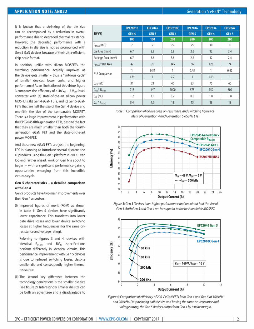
(I) Improved figures of merit (FOM) as shown in table 1: Gen 5 devices have significantly lower capacitance. This translates into lower gate drive losses and lower device switching losses at higher frequencies (for the same on-resistance and voltage rating).
Referring to figures 3 and 4, devices with identical RDS(on) and BVdss specifications perform differently in identical circuits. This performance improvement with Gen 5 devices is due to reduced switching losses, despite smaller die and consequently higher thermal resistance.
(II) The second key difference between the technology generations is the smaller die size (see figure 2): Interestingly, smaller die size can be both an advantage and a disadvantage to
96
95
94
93
92
91
90
89
88
87
86
85
840 2 4 6 8 10 12 14 16 18 20 22 24 26
Output Current (A)
Ecie
ncy (
%)
EPC2045 Generation 5Comparable RDS(on)
EPC2045 Gen 5EPC2001C Gen 4
BSZ097N10NS5
VIN = 48 V, VOUT = 5 V fSW = 500 kHz
200 kHz
100 kHz
200 kHz
100 kHz
EPC2010C Gen 4
EPC2046 Gen 5
98
96
94
92
90
88
86
840 2 4 6 8 10 12
Output Current (A)
Ecie
ncy (
%)
VIN = 160 V, VOUT = 16 V
Figure 3: Gen 5 Devices have higher performance and are about half the size of Gen 4. Both Gen 5 and Gen 4 are far superior to the best available MOSFET.
Table 1: Comparison of device area, on-resistance, and switching figures of Merit of Generation 4 and Generation 5 eGaN FETs
Figure 4: Comparison of efficiency of 200 V eGaN FETs from Gen 4 and Gen 5 at 100 kHz and 200 kHz. Despite being half the size and having the same on-resistance and
voltage rating, the Gen 5 devices outperform Gen 4 by a wide margin.
BV (V)EPC2001C EPC2045 EPC2010C EPC2046 EPC2034 EPC2047
GEN 4 GEN 5 GEN 4 GEN 5 GEN 4 GEN 5100 100 200 200 200 200
RDS(on) (mΩ) 7 7 25 25 10 10
Die Area (mm2) 6.7 3.8 5.8 2.6 12 7.4
Package Area (mm2) 6.7 3.8 5.8 2.6 12 7.4
RDS(on) * Die Area 47 26 145 66 120 74
R*A Comparison1 0.56 1 0.45 1 0.62
1.79 1 2.2 1 1.63 1
QOSS (nC) 31 21 40 23 75 60
QOSS * RDS(on) 217 147 1000 575 750 600
QGD (nC) 1.2 1.1 0.7 0.6 1.8 1.8
QGD * RDS(on) 8.4 7.7 18 15 18 18

APPLICATION NOTE: AN022
EPC – EFFICIENT POWER CONVERSION CORPORATION | WWW.EPC-CO.COM | COPYRIGHT 2017 | | 3
Generation 5 eGaN® Technology
the customer. It is an advantage in that smaller die require less space on the PCB. In addition, a smaller die has a greater ability to withstand a larger number of temperature cycles, as can be seen in figure 5 [2]. As an example, the Gen 5 200 V, 25mΩ EPC2046 can survive more than three times the number of power cycles with a temperature change of 100ºC compared with its Gen 4 counterpart, the EPC2010C (Note that the difference in power cycling performance between the Gen 4 EPC2034 and the Gen 5 EPC2047 is a modest 30%. This is due to the relatively small difference in the distance from the center of the die to the diagonal corner. It is this dimension that has the greatest impact on the temperature and power cycling capability of a device [2]). For demanding applications, such as telecom, automotive, or industrial, withstanding temperature and power cycles can be a big factor impacting the customer’s choice.
One other improvement in the 100 V and below Gen 5 product family is the increased spacing between the electrical terminals. Generation 4 products, rated at 100 V and below, have a 400 μm pitch. This tight pitch is sometimes challenging with low cost PCB manufacturers and thick copper traces. Generation 5 products at 100 V and below all now have a wider, 450 μm pitch. The 200 V Gen 5 product has maintained a 600 μm spacing consistent with Gen 4 (see figures 6 and 7).
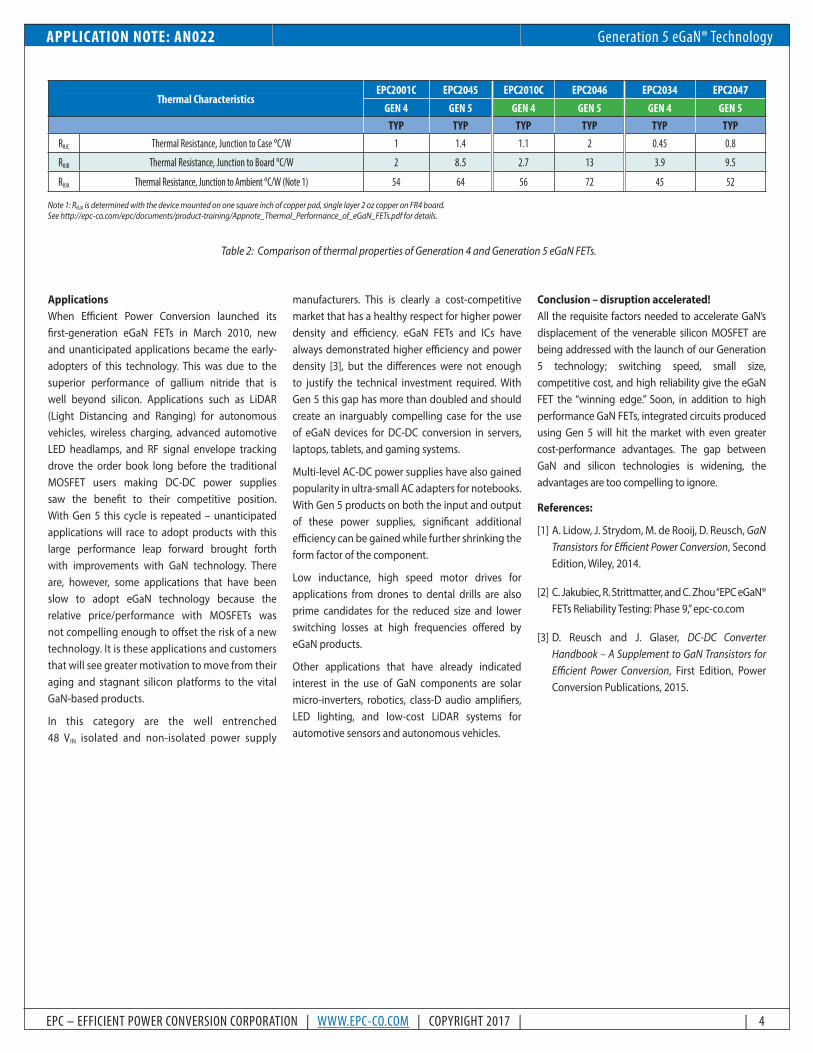
A disadvantage of a smaller Gen 5 die size is that the thermal resistance can be higher than with Gen 4 products. Table 2 shows a comparison of thermal resistance between Gen 4 and Gen 5 devices of similar RDS(on) and BV rating. Due to the chip-scale packaging of all EPC’s eGaN FETs and ICs, the effect of die size on thermal resistance is mitigated by two factors, (1) there is less thermal impedance between the chip-scale package and the ambient environment compared with packaged parts, and (2) the PCB design has the largest impact on thermal resistance when no heatsink is applied to the back surface of the die.
6
5
4
3
2
160 80 100 120 140 160 180
ΔT During IOL (C)
Impr
ovem
ent F
acto
r for
Cycle
s to F
ailu
re
EPC2045/EPC2001CEPC2046/EPC2010CEPC2047/EPC2034
1 4 7 10 13
2 5 8 11 14
3 6 9 12 15
B
c
d
e
DIMMICROMETERS
MIN Nominal MAX
A 2470 2500 2530
B 1470 1500 1530
c 450
d 500
e 238 264 290
Pad 1 is Gate;Pads 2, 3, 7, 9, 13, 14, 15 are Source;Pads 4, 5, 6, 10, 11, 12 are Drain;Pad 8 is substrate
A100 V EPC2045 Die Drawing – Bump View (Bump on Top)
1 3 5 7 9
Bc
d
e
2 4 6 8 10
A
DIMMICROMETERS
MIN Nominal MAX
A 2736 2766 2796
B 920 950 980
c 450
d 600
e 238 264 290
Pad 1 is Gate;Pads 2, 5, 6, 10 are Source;Pads 3, 4, 7, 8 are Drain;Pad 9 is substrate
200 V EPC2046 Device Drawing – Bump View (Bump on Top)
Figure 5. Shown is the relative power cycling performance of Gen 5 devices compared with Gen 4. Smaller die sizes have less differential thermal expansion
with the underlying PCB, thus reducing strain during thermo-mechanical cycling.
Figure 6: In comparison to Gen 4 devices, the pitch of 100 V Gen 5 transistors has been increased to 450 μm.
Figure 7: The pitch of 200 V Gen 5 transistors is the same as Gen 4 200 V at 600 μm.
APPLICATION NOTE: AN022
EPC – EFFICIENT POWER CONVERSION CORPORATION | WWW.EPC-CO.COM | COPYRIGHT 2017 | | 4
Generation 5 eGaN® Technology
Applications When Efficient Power Conversion launched its first-generation eGaN FETs in March 2010, new and unanticipated applications became the early-adopters of this technology. This was due to the superior performance of gallium nitride that is well beyond silicon. Applications such as LiDAR (Light Distancing and Ranging) for autonomous vehicles, wireless charging, advanced automotive LED headlamps, and RF signal envelope tracking drove the order book long before the traditional MOSFET users making DC-DC power supplies saw the benefit to their competitive position. With Gen 5 this cycle is repeated – unanticipated applications will race to adopt products with this large performance leap forward brought forth with improvements with GaN technology. There are, however, some applications that have been slow to adopt eGaN technology because the relative price/performance with MOSFETs was not compelling enough to offset the risk of a new technology. It is these applications and customers that will see greater motivation to move from their aging and stagnant silicon platforms to the vital GaN-based products.
In this category are the well entrenched 48 VIN isolated and non-isolated power supply
manufacturers. This is clearly a cost-competitive market that has a healthy respect for higher power density and efficiency. eGaN FETs and ICs have always demonstrated higher efficiency and power density [3], but the differences were not enough to justify the technical investment required. With Gen 5 this gap has more than doubled and should create an inarguably compelling case for the use of eGaN devices for DC-DC conversion in servers, laptops, tablets, and gaming systems.
Multi-level AC-DC power supplies have also gained popularity in ultra-small AC adapters for notebooks. With Gen 5 products on both the input and output of these power supplies, significant additional efficiency can be gained while further shrinking the form factor of the component.
Low inductance, high speed motor drives for applications from drones to dental drills are also prime candidates for the reduced size and lower switching losses at high frequencies offered by eGaN products.
Other applications that have already indicated interest in the use of GaN components are solar micro-inverters, robotics, class-D audio amplifiers, LED lighting, and low-cost LiDAR systems for automotive sensors and autonomous vehicles.
Conclusion – disruption accelerated!All the requisite factors needed to accelerate GaN’s displacement of the venerable silicon MOSFET are being addressed with the launch of our Generation 5 technology; switching speed, small size, competitive cost, and high reliability give the eGaN FET the “winning edge.” Soon, in addition to high performance GaN FETs, integrated circuits produced using Gen 5 will hit the market with even greater cost-performance advantages. The gap between GaN and silicon technologies is widening, the advantages are too compelling to ignore.
References:
[1] A. Lidow, J. Strydom, M. de Rooij, D. Reusch, GaN Transistors for Efficient Power Conversion, Second Edition, Wiley, 2014.
[2] C. Jakubiec, R. Strittmatter, and C. Zhou “EPC eGaN® FETs Reliability Testing: Phase 9,” epc-co.com
[3] D. Reusch and J. Glaser, DC-DC Converter Handbook – A Supplement to GaN Transistors for Efficient Power Conversion, First Edition, Power Conversion Publications, 2015.
Note 1: RθJA is determined with the device mounted on one square inch of copper pad, single layer 2 oz copper on FR4 board. See http://epc-co.com/epc/documents/product-training/Appnote_Thermal_Performance_of_eGaN_FETs.pdf for details.
Thermal CharacteristicsEPC2001C EPC2045 EPC2010C EPC2046 EPC2034 EPC2047
GEN 4 GEN 5 GEN 4 GEN 5 GEN 4 GEN 5TYP TYP TYP TYP TYP TYP
RθJC Thermal Resistance, Junction to Case ºC/W 1 1.4 1.1 2 0.45 0.8
RθJB Thermal Resistance, Junction to Board ºC/W 2 8.5 2.7 13 3.9 9.5
RθJA Thermal Resistance, Junction to Ambient ºC/W (Note 1) 54 64 56 72 45 52
Table 2: Comparison of thermal properties of Generation 4 and Generation 5 eGaN FETs.
APPLICATION NOTE: AN022
EPC – EFFICIENT POWER CONVERSION CORPORATION | WWW.EPC-CO.COM | COPYRIGHT 2017 | | 5
Generation 5 eGaN® Technology
Appendix I: EPC 2045 Preliminary Data Sheet
EPC2045 – Enhancement-Mode Power Transistor Preliminary Specification Sheet
Status: EngineeringFeatures:• VDS, 100 V
• Maximum RDS(on), 7 mΩ
• ID, 16 A
Applications:• Open Rack Server Architectures
• LiDAR/Pulsed Power Applications
• USB-C
• Isolated Power Supplies
• Point of Load Converters
• Class D Audio
• LED Lighting
• Low Inductance Motor Drive
EPC2045 eGaN® FETs are supplied in passivated die form with solder bumps.
Die Size: 2.5 mm x 1.5 mm
Note 1: RθJA is determined with the device mounted on one square inch of copper pad, single layer 2 oz copper on FR4 board. See http://epc-co.com/epc/documents/product-training/Appnote_Thermal_Performance_of_eGaN_FETs.pdf for details.
All measurements were done with substrate shorted to source.
Thermal CharacteristicsTYP UNIT
RθJC Thermal Resistance, Junction to Case 1.4 ˚C/W
RθJB Thermal Resistance, Junction to Board 8.5 ˚C/W
RθJA Thermal Resistance, Junction to Ambient (Note 1) 64 ˚C/W
Maximum Ratings
VDS
Drain-to-Source Voltage (Continuous) 100V
Drain-to-Source Voltage (up to 10,000 5 ms pulses at 150°C) 120
ID
Continuous (TA = 25˚C, RθJA= 38˚C/W) 16A
Pulsed (25˚C, TPulse = 300 µs) 130
VGS
Gate-to-Source Voltage 6V
Gate-to-Source Voltage -4
TJ Operating Temperature -40 to 150˚C
TSTG Storage Temperature -40 to 150
Static CharacteristicsTYP MIN TYP MAX UNIT
BVDSS Drain-to-Source Voltage VGS = 0 V, ID = 0.3 mA 100 V
IDSS Drain Source Leakage VDS = 80 V, VGS = 0 V 0.1 0.25 mA
IGSS
Gate-to-Source Forward Leakage VGS = 5 V 1 5 mA
Gate-to-Source Reverse Leakage VGS = −4 V 0.1 0.25 mA
VGS(TH) Gate Threshold Voltage VDS = VGS, ID = 5 mA 0.8 1.5 2.5 V
RDS(on) Drain-Source On Resistance VGS = 5 V, ID = 16 A 5.6 7 mΩ
VSD Source-Drain Forward Voltage IS = 0.5 A, VGS = 0 V 1.9 V
APPLICATION NOTE: AN022
EPC – EFFICIENT POWER CONVERSION CORPORATION | WWW.EPC-CO.COM | COPYRIGHT 2017 | | 6
Generation 5 eGaN® Technology
Note 2: COSS(ER) is a fixed capacitance that gives the same stored energy as COSS while VDS is rising from 0 to 50% BVDSS. Note 3: COSS(TR) is a fixed capacitance that gives the same charging time as COSS while VDS is rising from 0 to 50% BVDSS. All measurements were done with substrate shorted to source.
Dynamic CharacteristicsPARAMETER TEST CONDITIONS MIN TYP MAX UNIT
CISS Input Capacitance
VDS = 50 V, VGS = 0 V
570 685
pF
CRSS Reverse Transfer Capacitance 5
COSS Output Capacitance 260 390
COSS(ER)Effective Output Capacitance, Energy Related (Note 2)
VDS = 0 to 50 V, VGS = 0 V 320
COSS(TR)Effective Output Capacitance, Time Related (Note 3) 420
RG Gate Resistance 0.6 Ω
QG Total Gate Charge VDS = 50 V, VGS = 5 V, ID = 16 A 5.2 6.5
nC
QGS Gate to Source Charge
VDS = 50 V, ID = 16 A
1.7
QGD Gate to Drain Charge 1.1
QG(TH) Gate Charge at Threshold 1.2
QOSS Output Charge VDS = 50 V, VGS = 0 V 21 32
QRR Source-Drain Recovery Charge 0
125
100
75
50
25
00 0.5 1.0 1.5 2.0 3.02.5
I D – D
rain
Curre
nt (A
)
VDS – Drain-to-Source Voltage (V)
VGS = 5 VVGS = 4 VVGS = 3 VVGS = 2 V
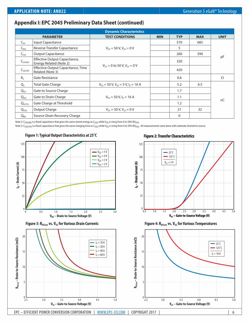
Figure 1: Typical Output Characteristics at 25°C
125
100
75
50
25
04.5 4.0 5.00.5 1.0 1.5 2.0 3.0 3.52.5
I D –
Dra
in Cu
rrent
(A)
VGS – Gate-to-Source Voltage (V)
Figure 2: Transfer Characteristics
25˚C125˚C
VDS = 3 V
I D –
Dra
in Cu
rrent
(A)
VGS – Gate-to-Source Voltage (V)
Figure 2: Transfer Characteristics
25˚C125˚C
VDS = 3 V
Appendix I: EPC 2045 Preliminary Data Sheet (continued)R D
S(on
) – D
rain
-to-S
ourc
e Res
istan
ce (m
Ω)
VGS – Gate-to-Source Voltage (V) 2.5 3.0 3.5 4.0 4.5 5.0
Figure 3: RDS(on) vs. VGS for Various Drain Currents
ID = 10 AID = 20 AID = 40 AID = 80 A
20
15
10
5
02.5 3.0 3.5 4.0 4.5 5.0
Figure 4: RDS(on) vs. VGS for Various Temperatures
25˚C125˚C
ID = 16 A
R DS(
on) –
Dra
in-to
-Sou
rce R
esist
ance
(mΩ
)
VGS – Gate-to-Source Voltage (V)
20
15
10
5
0
APPLICATION NOTE: AN022
EPC – EFFICIENT POWER CONVERSION CORPORATION | WWW.EPC-CO.COM | COPYRIGHT 2017 | | 7
Generation 5 eGaN® Technology
1000
800
600
400
200
0
Capa
citan
ce (p
F)
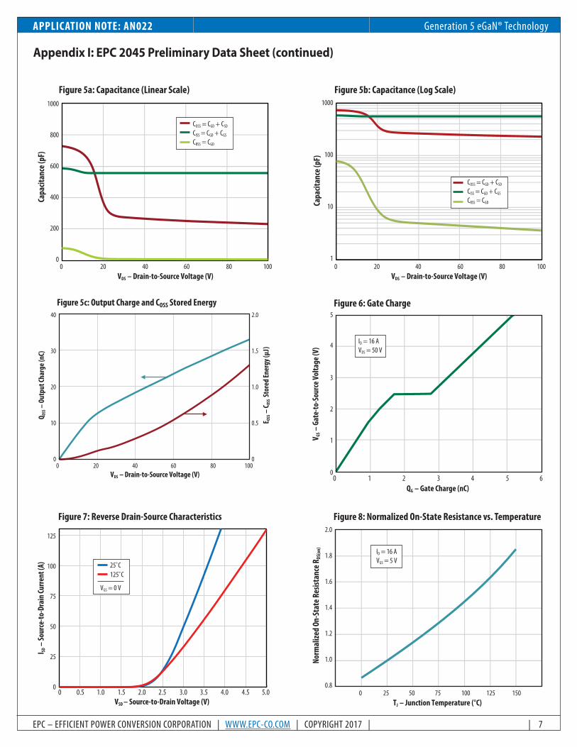
Figure 5a: Capacitance (Linear Scale)
COSS = CGD + CSD
CISS = CGD + CGS
CRSS = CGD
0 20 40 60 80 100 VDS – Drain-to-Source Voltage (V)
0 20 40 60 80 100
Figure 5c: Output Charge and COSS Stored Energy
E OSS
– C O
SS S
tore
d Ene
rgy (
μJ)
Q OSS
– O
utpu
t Cha
rge (
nC)
VDS – Drain-to-Source Voltage (V)
40
30
20
10
0
2.0
1.5
1.0
0.5
0
Capa
citan
ce (p
F)
1000
100
10
10 20 40 60 80 100
Figure 5b: Capacitance (Log Scale)
VDS – Drain-to-Source Voltage (V)
COSS = CGD + CSD
CISS = CGD + CGS
CRSS = CGD
0 1 2 3 4 5 6
Figure 6: Gate Charge
ID = 16 AVDS = 50 V
V GS
– Ga
te-to
-Sou
rce V
olta
ge (V
)
QG – Gate Charge (nC)
5
4
3
2
1
0
Appendix I: EPC 2045 Preliminary Data Sheet (continued)
0.50 1.0 1.5 2.0 2.5 3.0 3.5 4.0 4.5 5.0
I SD –
Sour
ce-to
-Dra
in Cu
rrent
(A)
VSD – Source-to-Drain Voltage (V)
Figure 7: Reverse Drain-Source Characteristics
125
100
75
50
25
0
25˚C125˚C
VGS = 0 V
Figure 8: Normalized On-State Resistance vs. Temperature
ID = 16 AVGS = 5 V
Norm
alize
d On
-Sta
te R
esist
ance
RDS
(on)
2.0
1.8
1.6
1.4
1.2
1.0
0.80 25 50 75 100 125 150
TJ – Junction Temperature (°C)
APPLICATION NOTE: AN022
EPC – EFFICIENT POWER CONVERSION CORPORATION | WWW.EPC-CO.COM | COPYRIGHT 2017 | | 8
Generation 5 eGaN® Technology
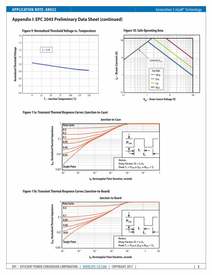
Figure 9: Normalized Threshold Voltage vs. Temperature
Norm
alize
d Th
resh
old
Volta
ge
1.4
1.3
1.2
1.1
1.0
0.9
0.8
0.7
0.60 25 50 75 100 125 150
TJ – Junction Temperature (°C)
ID = 5 mA
100
10
1
0.10.1 1 10 100
Limited by RDS(on)
Pulse Width 100 ms 10 ms 1 ms 100 μs
Figure 10: Safe Operating Area
I D –
Drai
n Cu
rren
t (A)
VDS – Drain-Source Voltage (V)
Appendix I: EPC 2045 Preliminary Data Sheet (continued)
tp, Rectangular Pulse Duration, seconds
Z θJC
, Nor
mal
ized T
herm
al Im
peda
nce
0.5
0.05
0.02
Single Pulse
0.01
0.10.2
Duty Cycle:
Junction-to-Case
Notes:Duty Factor: D = t1/t2
Peak TJ = PDM x ZθJC x RθJC + TC
PDM
t1
t2
10-5 10-4 10-3 10-2 10-110-6 1
1
0.1
0.01
0.001
tp, Rectangular Pulse Duration, seconds
Z θJB
, Nor
mal
ized T
herm
al Im
peda
nce
0.5
0.1
0.02
0.05
Single Pulse
0.01
Duty Cycle:
Junction-to-Board
Notes:Duty Factor: D = t1/t2
Peak TJ = PDM x ZθJB x RθJB + TB
PDM
t1
t2
10-5 10-4 10-3 10-2 10-1 1 101
1
0.1
0.01
0.001
Figure 11a: Transient Thermal Response Curves (Junction-to-Case)
Figure 11b: Transient Thermal Response Curves (Junction-to-Board)
APPLICATION NOTE: AN022
EPC – EFFICIENT POWER CONVERSION CORPORATION | WWW.EPC-CO.COM | COPYRIGHT 2017 | | 9
Generation 5 eGaN® Technology
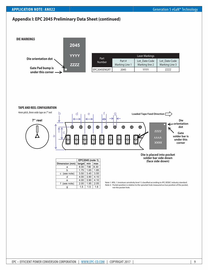
Appendix I: EPC 2045 Preliminary Data Sheet (continued)
2045
YYYY
ZZZZ Die orientation dot
Gate Pad bump is under this corner
Part Number
Laser Markings
Part #Marking Line 1
Lot_Date CodeMarking line 2
Lot_Date CodeMarking Line 3
EPC2045ENGRT 2045 YYYY ZZZZ
TAPE AND REEL CONFIGURATION4mm pitch, 8mm wide tape on 7” reel
7” reel
a
d e f g
c
b
EPC2045 (note 1) Dimension (mm) target min max
a 8.00 7.90 8.30 b 1.75 1.65 1.85
c (see note) 3.50 3.45 3.55 d 4.00 3.90 4.10 e 4.00 3.90 4.10
f (see note) 2.00 1.95 2.05 g 1.5 1.5 1.6
Note 1: MSL 1 (moisture sensitivity level 1) classied according to IPC/JEDEC industry standard.Note 2: Pocket position is relative to the sprocket hole measured as true position of the pocket, not the pocket hole.
Dieorientation
dot
Gatesolder bar is
under thiscorner
Die is placed into pocketsolder bar side down
(face side down)
Loaded Tape Feed Direction
DIE MARKINGS

APPLICATION NOTE: AN022
EPC – EFFICIENT POWER CONVERSION CORPORATION | WWW.EPC-CO.COM | COPYRIGHT 2017 | | 10
Generation 5 eGaN® Technology
B
A
d
ec
5 112 8 14
101 7 134
156 123 9
DIM MICROMETERS
A 2500
B 1500
c 450
d 500
e 230
Pad 1 is Gate;Pads 2, 3, 7, 9, 13, 14, 15 are Source;Pads 4, 5, 6, 10, 11, 12 are Drain;Pad 8 is substrate
B
A
d
g
h
c
5 112 8 14
101 7 134
156 123 9
DIM MICROMETERS
A 2500
B 1500
c 450
d 500
g 300
250h
Appendix I: EPC 2045 Preliminary Data Sheet (continued)
510
SEATING PLANE
790
280 =
+/−
28
B
A
d
ec
15
5
101
6
112
7
12
8
13
3 9
14
4
DIMMICROMETERS
MIN Nominal MAX
A 2470 2500 2530
B 1470 1500 1530
c 450
d 500
e 238 264 290
Pad 1 is Gate;Pads 2, 3, 7, 9, 13, 14, 15 are Source;Pads 4, 5, 6, 10, 11, 12 are Drain;Pad 8 is substrate
The land pattern is solder mask defined Solder mask is 10μm smaller per side than bump
DIE OUTLINESolder Bar View
Side View
RECOMMENDEDLAND PATTERN (measurements in µm)
RECOMMENDEDSTENCIL DRAWING (measurements in µm)
Recommended stencil should be 4mil (100µm) thick, must be laser cut, openings per drawing. The corner has a radius of R60Intended for use with SAC305 Type 4 solder, reference 88.5% metals content.Additional assembly resources available at http://epc-co.com/epc/DesignSupport/AssemblyBasics.aspx
APPLICATION NOTE: AN022
EPC – EFFICIENT POWER CONVERSION CORPORATION | WWW.EPC-CO.COM | COPYRIGHT 2017 | | 11
Generation 5 eGaN® Technology
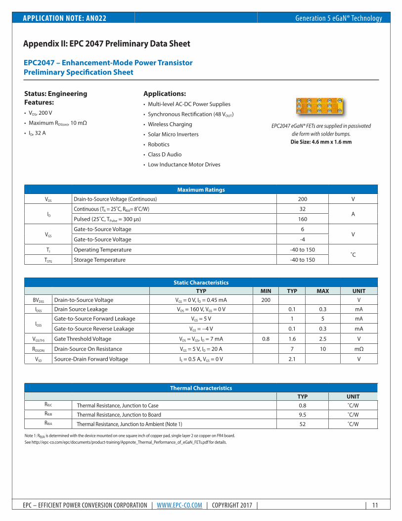
Appendix II: EPC 2047 Preliminary Data Sheet
EPC2047 – Enhancement-Mode Power Transistor Preliminary Specification Sheet
Status: EngineeringFeatures:• VDS, 200 V
• Maximum RDS(on), 10 mΩ
• ID, 32 A
Applications:• Multi-level AC-DC Power Supplies
• Synchronous Rectification (48 VOUT)
• Wireless Charging
• Solar Micro Inverters
• Robotics
• Class D Audio
• Low Inductance Motor Drives
EPC2047 eGaN® FETs are supplied in passivated die form with solder bumps.
Die Size: 4.6 mm x 1.6 mm
Note 1: RθJA is determined with the device mounted on one square inch of copper pad, single layer 2 oz copper on FR4 board. See http://epc-co.com/epc/documents/product-training/Appnote_Thermal_Performance_of_eGaN_FETs.pdf for details.
Thermal CharacteristicsTYP UNIT
RθJC Thermal Resistance, Junction to Case 0.8 ˚C/WRθJB Thermal Resistance, Junction to Board 9.5 ˚C/WRθJA Thermal Resistance, Junction to Ambient (Note 1) 52 ˚C/W
Maximum Ratings
VDS Drain-to-Source Voltage (Continuous) 200 V
ID
Continuous (TA = 25˚C, RθJA= 8˚C/W) 32A
Pulsed (25˚C, TPulse = 300 µs) 160
VGS
Gate-to-Source Voltage 6V
Gate-to-Source Voltage -4
TJ Operating Temperature -40 to 150˚C
TSTG Storage Temperature -40 to 150
Static CharacteristicsTYP MIN TYP MAX UNIT
BVDSS Drain-to-Source Voltage VGS = 0 V, ID = 0.45 mA 200 V
IDSS Drain Source Leakage VDS = 160 V, VGS = 0 V 0.1 0.3 mA
IGSS
Gate-to-Source Forward Leakage VGS = 5 V 1 5 mA
Gate-to-Source Reverse Leakage VGS = −4 V 0.1 0.3 mA
VGS(TH) Gate Threshold Voltage VDS = VGS, ID = 7 mA 0.8 1.6 2.5 V
RDS(ON) Drain-Source On Resistance VGS = 5 V, ID = 20 A 7 10 mΩ
VSD Source-Drain Forward Voltage IS = 0.5 A, VGS = 0 V 2.1 V
APPLICATION NOTE: AN022
EPC – EFFICIENT POWER CONVERSION CORPORATION | WWW.EPC-CO.COM | COPYRIGHT 2017 | | 12
Generation 5 eGaN® Technology
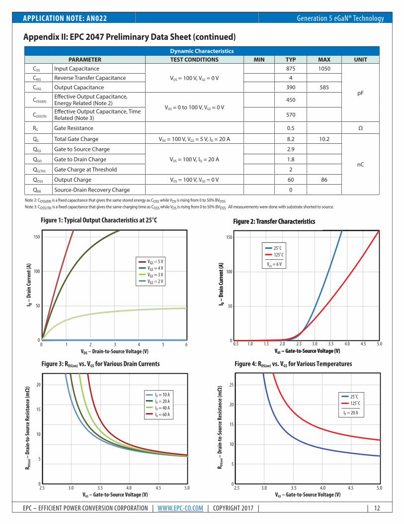
Dynamic CharacteristicsPARAMETER TEST CONDITIONS MIN TYP MAX UNIT
CISS Input Capacitance
VDS = 100 V, VGS = 0 V
875 1050
pF
CRSS Reverse Transfer Capacitance 4
COSS Output Capacitance 390 585
COSS(ER)Effective Output Capacitance, Energy Related (Note 2)
VDS = 0 to 100 V, VGS = 0 V 450
COSS(TR)Effective Output Capacitance, Time Related (Note 3) 570
RG Gate Resistance 0.5 Ω
QG Total Gate Charge VDS = 100 V, VGS = 5 V, ID = 20 A 8.2 10.2
nC
QGS Gate to Source Charge
VDS = 100 V, ID = 20 A
2.9
QGD Gate to Drain Charge 1.8
QG(TH) Gate Charge at Threshold 2
QOSS Output Charge VDS = 100 V, VGS = 0 V 60 86
QRR Source-Drain Recovery Charge 0
Appendix II: EPC 2047 Preliminary Data Sheet (continued)
150
100
50
00 1 2 3 4 65
I D – D
rain
Curre
nt (A
)
VDS – Drain-to-Source Voltage (V)
Figure 1: Typical Output Characteristics at 25°C
VGS = 5 VVGS = 4 VVGS = 3 VVGS = 2 V
150
100
50
00.5 1.0 1.5 2.0 3.0 3.5 4.0 4.5 5.02.5
I D –
Dra
in Cu
rrent
(A)
VGS – Gate-to-Source Voltage (V)
Figure 2: Transfer Characteristics
25˚C125˚C
VDS = 3 V
I D –
Dra
in Cu
rrent
(A)
VGS – Gate-to-Source Voltage (V)
Figure 2: Transfer Characteristics
25˚C125˚C
VDS = 6 V
R DS(
on) –
Dra
in-to
-Sou
rce R
esist
ance
(mΩ
)
VGS – Gate-to-Source Voltage (V) 2.5 3.0 3.5 4.0 4.5 5.0
Figure 3: RDS(on) vs. VGS for Various Drain Currents
ID = 10 AID = 20 AID = 40 AID = 60 A
20
15
10
5
02.5 3.0 3.5 4.0 4.5 5.0
Figure 4: RDS(on) vs. VGS for Various Temperatures
25˚C125˚C
ID = 20 A
R DS(
on) –
Dra
in-to
-Sou
rce R
esist
ance
(mΩ
)
VGS – Gate-to-Source Voltage (V)
25
20
15
10
5
0
Note 2: COSS(ER) is a fixed capacitance that gives the same stored energy as COSS while VDS is rising from 0 to 50% BVDSS. Note 3: COSS(TR) is a fixed capacitance that gives the same charging time as COSS while VDS is rising from 0 to 50% BVDSS. All measurements were done with substrate shorted to source.
APPLICATION NOTE: AN022
EPC – EFFICIENT POWER CONVERSION CORPORATION | WWW.EPC-CO.COM | COPYRIGHT 2017 | | 13
Generation 5 eGaN® Technology
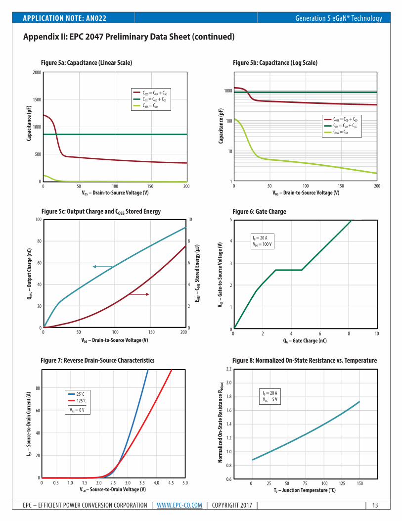
2000
1500
1000
500
0
Capa
citan
ce (p
F)
Figure 5a: Capacitance (Linear Scale)
COSS = CGD + CSD
CISS = CGD + CGS
CRSS = CGD
VDS – Drain-to-Source Voltage (V) 0 50 100 150 200
0 50 100 150 200
Figure 5c: Output Charge and COSS Stored Energy
Q OSS
– O
utpu
t Cha
rge (
nC)
E OSS
– C O
SS S
tore
d Ene
rgy (
μJ)
VDS – Drain-to-Source Voltage (V)
100
80
60
40
20
0
10
8
6
4
2
0
Capa
citan
ce (p
F)
1000
100
10
10 50 100 150 200
Figure 5b: Capacitance (Log Scale)
VDS – Drain-to-Source Voltage (V)
COSS = CGD + CSD
CISS = CGD + CGS
CRSS = CGD
0 2 4 6 8 10
Figure 6: Gate Charge
ID = 20 AVDS = 100 V
V GS
– Ga
te-to
-Sou
rce V
olta
ge (V
)
QG – Gate Charge (nC)
5
4
3
2
1
0
Appendix II: EPC 2047 Preliminary Data Sheet (continued)
0.50 1.0 1.5 2.0 2.5 3.0 3.5 4.0 4.5 5.0
I SD –
Sour
ce-to
-Dra
in Cu
rrent
(A)
VSD – Source-to-Drain Voltage (V)
Figure 7: Reverse Drain-Source Characteristics
80
60
40
20
0
25˚C125˚C
VGS = 0 V
Figure 8: Normalized On-State Resistance vs. Temperature
ID = 20 AVGS = 5 V
Norm
alize
d On
-Sta
te R
esist
ance
RDS
(on)
2.2
2.0
1.8
1.6
1.4
1.2
1.0
0.8
0.60 25 50 75 100 125 150
TJ – Junction Temperature (°C)
APPLICATION NOTE: AN022
EPC – EFFICIENT POWER CONVERSION CORPORATION | WWW.EPC-CO.COM | COPYRIGHT 2017 | | 14
Generation 5 eGaN® Technology
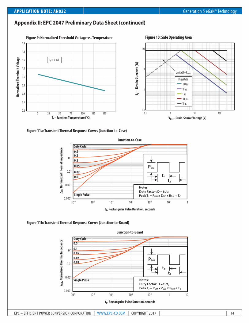
Figure 9: Normalized Threshold Voltage vs. Temperature
0 25 50 75 100 125 150 TJ – Junction Temperature (°C)
ID = 7 mA
Norm
alize
d Th
resh
old
Volta
ge
1.4
1.3
1.2
1.1
1.0
0.9
0.8
0.7
0.6
100
10
1
0.10.1 1 10 100
Limited by RDS(on)
Pulse Width 100 ms 10 ms 1 ms 100 μs 10 μs
I D –
Drai
n Cu
rren
t (A)
Figure 10: Safe Operating Area
VDS – Drain-Source Voltage (V)
Appendix II: EPC 2047 Preliminary Data Sheet (continued)
tp, Rectangular Pulse Duration, seconds
Z θJB
, Nor
mal
ized T
herm
al Im
peda
nce
0.5
0.050.02
Single Pulse
0.01
0.1
Duty Cycle:
Junction-to-Board
Notes:Duty Factor: D = t1/t2
Peak TJ = PDM x ZθJB x RθJB + TB
PDM
t1
t2
10-5 10-4 10-3 10-2 10-1 101
1
0.1
0.01
0.001
0.0001
tp, Rectangular Pulse Duration, seconds
Z θJC
, Nor
mal
ized T
herm
al Im
peda
nce
0.50.20.1
0.02
0.05
Single Pulse
0.01
Duty Cycle:
Junction-to-Case
Notes:Duty Factor: D = t1/t2
Peak TJ = PDM x ZθJC x RθJC + TC
PDM
t1
t2
10-6 10-5 10-4 10-3 10-2 10-1 1
1
0.1
0.01
0.001
0.0001
Figure 11a: Transient Thermal Response Curves (Junction-to-Case)
Figure 11b: Transient Thermal Response Curves (Junction-to-Board)
APPLICATION NOTE: AN022
EPC – EFFICIENT POWER CONVERSION CORPORATION | WWW.EPC-CO.COM | COPYRIGHT 2017 | | 15
Generation 5 eGaN® Technology
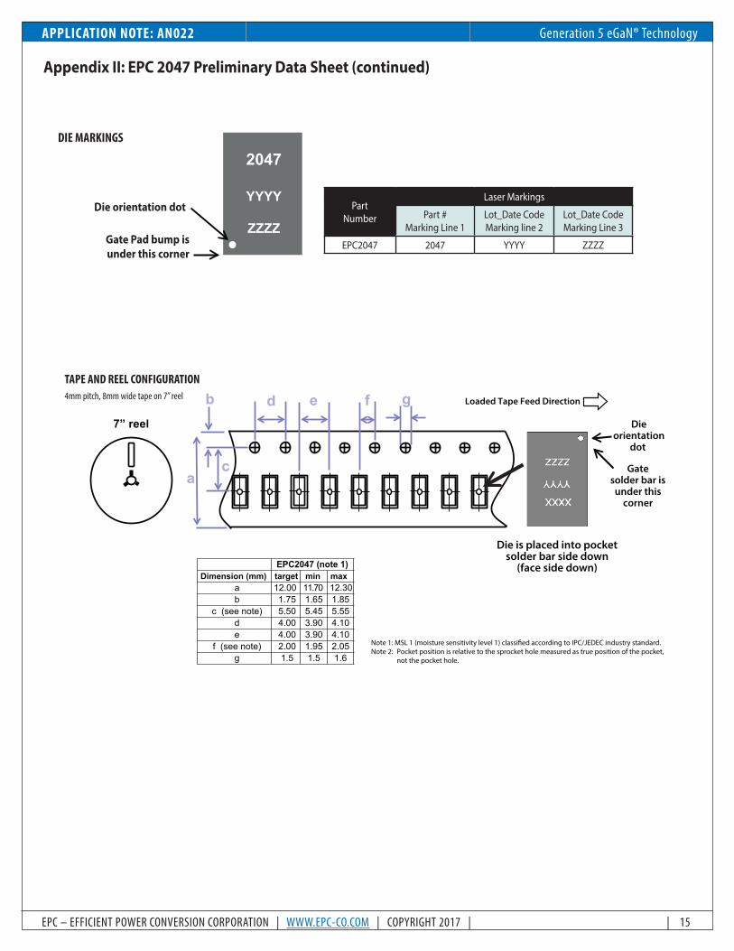
Appendix II: EPC 2047 Preliminary Data Sheet (continued)
2047
YYYY
ZZZZ Die orientation dot
Gate Pad bump is under this corner
Part Number
Laser Markings
Part #Marking Line 1
Lot_Date CodeMarking line 2
Lot_Date CodeMarking Line 3
EPC2047 2047 YYYY ZZZZ
TAPE AND REEL CONFIGURATION4mm pitch, 8mm wide tape on 7” reel
7” reel
a
d e f g
c
b
EPC2047 (note 1) Dimension (mm) target min max
a 12.00 11.70 12.30 b 1.75 1.65 1.85
c (see note) 5.50 5.45 5.55 d 4.00 3.90 4.10 e 4.00 3.90 4.10
f (see note) 2.00 1.95 2.05 g 1.5 1.5 1.6
Note 1: MSL 1 (moisture sensitivity level 1) classied according to IPC/JEDEC industry standard.Note 2: Pocket position is relative to the sprocket hole measured as true position of the pocket, not the pocket hole.
Dieorientation
dot
Gatesolder bar is
under thiscorner
Die is placed into pocketsolder bar side down
(face side down)
Loaded Tape Feed Direction
DIE MARKINGS
APPLICATION NOTE: AN022
EPC – EFFICIENT POWER CONVERSION CORPORATION | WWW.EPC-CO.COM | COPYRIGHT 2017 | | 16
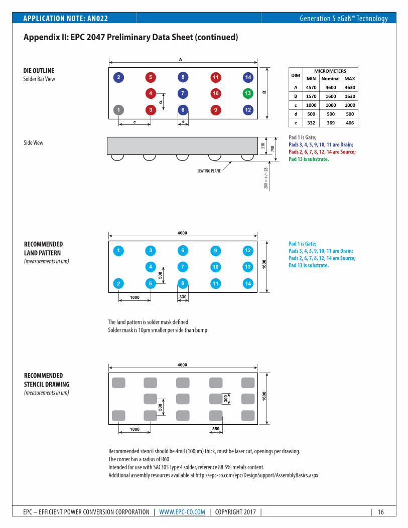
Generation 5 eGaN® Technology
1600
4600
500
3301000
4 107 13
91 6 123
145 112 8
Pad 1 is Gate;Pads 3, 4, 5, 9, 10, 11 are Drain;Pads 2, 6, 7, 8, 12, 14 are Source;Pad 13 is substrate.
1600
4600
500
300
3501000
Appendix II: EPC 2047 Preliminary Data Sheet (continued)
510
SEATING PLANE
790
280 =
+/−
28
B
A
d
ec
14
4
91
5
10
6
11
7
12
2 8
13
3
DIMMICROMETERS
MIN Nominal MAX
A
B
c
d
e
4570
1570
1000
500
332
4600
1600
1000
500
369
4630
1630
1000
500
406
Pad 1 is Gate;Pads 3, 4, 5, 9, 10, 11 are Drain;Pads 2, 6, 7, 8, 12, 14 are Source;Pad 13 is substrate.
The land pattern is solder mask defined Solder mask is 10μm smaller per side than bump
DIE OUTLINESolder Bar View
Side View
RECOMMENDEDLAND PATTERN (measurements in µm)
RECOMMENDEDSTENCIL DRAWING (measurements in µm)
Recommended stencil should be 4mil (100µm) thick, must be laser cut, openings per drawing. The corner has a radius of R60Intended for use with SAC305 Type 4 solder, reference 88.5% metals content.Additional assembly resources available at http://epc-co.com/epc/DesignSupport/AssemblyBasics.aspx
APPLICATION NOTE: AN022
EPC – EFFICIENT POWER CONVERSION CORPORATION | WWW.EPC-CO.COM | COPYRIGHT 2017 | | 17
Generation 5 eGaN® Technology
Appendix III: The Journey to Generation 5
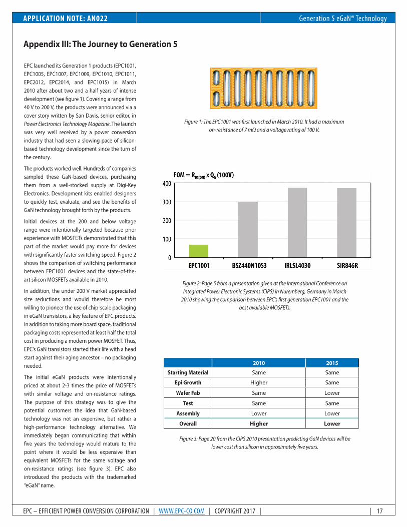
EPC launched its Generation 1 products (EPC1001, EPC1005, EPC1007, EPC1009, EPC1010, EPC1011, EPC2012, EPC2014, and EPC1015) in March 2010 after about two and a half years of intense development (see figure 1). Covering a range from 40 V to 200 V, the products were announced via a cover story written by San Davis, senior editor, in Power Electronics Technology Magazine. The launch was very well received by a power conversion industry that had seen a slowing pace of silicon-based technology development since the turn of the century.
The products worked well. Hundreds of companies sampled these GaN-based devices, purchasing them from a well-stocked supply at Digi-Key Electronics. Development kits enabled designers to quickly test, evaluate, and see the benefits of GaN technology brought forth by the products.
Initial devices at the 200 and below voltage range were intentionally targeted because prior experience with MOSFETs demonstrated that this part of the market would pay more for devices with significantly faster switching speed. Figure 2 shows the comparison of switching performance between EPC1001 devices and the state-of-the-art silicon MOSFETs available in 2010.
In addition, the under 200 V market appreciated size reductions and would therefore be most willing to pioneer the use of chip-scale packaging in eGaN transistors, a key feature of EPC products. In addition to taking more board space, traditional packaging costs represented at least half the total cost in producing a modern power MOSFET. Thus, EPC’s GaN transistors started their life with a head start against their aging ancestor – no packaging needed.
The initial eGaN products were intentionally priced at about 2-3 times the price of MOSFETs with similar voltage and on-resistance ratings. The purpose of this strategy was to give the potential customers the idea that GaN-based technology was not an expensive, but rather a high-performance technology alternative. We immediately began communicating that within five years the technology would mature to the point where it would be less expensive than equivalent MOSFETs for the same voltage and on-resistance ratings (see figure 3). EPC also introduced the products with the trademarked “eGaN” name.
Figure 1: The EPC1001 was first launched in March 2010. It had a maximum on-resistance of 7 mΩ and a voltage rating of 100 V.
Figure 2: Page 5 from a presentation given at the International Conference on Integrated Power Electronic Systems (CIPS) in Nuremberg, Germany in March
2010 showing the comparison between EPC’s first generation EPC1001 and the best available MOSFETs.
Figure 3: Page 20 from the CIPS 2010 presentation predicting GaN devices will be lower cost than silicon in approximately five years.
2010 2015
Starting Material Same Same
Epi Growth Higher Same
Wafer Fab Same Lower
Test Same Same
Assembly Lower Lower
Overall Higher Lower
APPLICATION NOTE: AN022
EPC – EFFICIENT POWER CONVERSION CORPORATION | WWW.EPC-CO.COM | COPYRIGHT 2017 | | 18
Generation 5 eGaN® Technology
At that time the initial eGaN products were being launched, EPC took the first steps in educating the power conversion community on the four things to look for in the coming years that would indicate GaN readiness to obsolete the aging silicon MOSFET (see figure 4).
It quickly came to light that there were several barriers to widespread adoption of GaN. The first was how to drive the gate and a second was to overcome how to minimize the parasitic inductances coming to light because of the rapid switching speed of GaN transistors.
Although enhancement-mode GaN transistors are conceptually easy to use because they are normally “off” (enhancement-mode) transistors just like their MOSFET predecessors, the nuanced differences when placed into circuits took a significant amount of work by design engineers to overcome.
Two key categories of difficulty were (a) how to drive the gate without exceeding the 6 V maximum rating, and (b) how to do a circuit layout to minimize parasitic inductances. With the increased switching speed capability of the eGaN FETs, di/dt (the speed of change of current) increased to unprecedented values. Since voltage overshoot in a circuit is proportional to L di/dt, where “L” is the inductance in the circuit, voltage overshoot was large when FETs were switched quickly and there was significant parasitic inductance in the circuit.
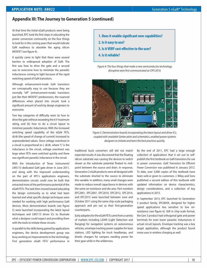
With the introduction of Texas Instruments’ LM5113 dedicated GaN gate driver in June 2011, and along with the improved understanding on the part of EPC’s applications engineers, demonstration circuits could now be built that extracted more of the performance potential of the eGaN FETs. The task then moved toward educating the design community as to what had been learned and what specific design techniques were needed for working with high performance GaN devices. More demonstration boards (see figure 5) were launched incorporating the latest layout techniques and LM5113 driver ICs to illustrate what a designer could expect and providing them with the tools to imitate these circuits.
In parallel to the skills being gained by applications engineers, the device development group was busy working on improvements to the technology. First generation eGaN FETs’ performance in
Appendix III: The Journey to Generation 5 (continued)
Figure 4: The four things that make a new semiconductor technology disruptive were first communicated at CIPS 2010.
Figure 5: Demonstration boards incorporating the latest layout and driver ICs, coupled with available Gerber plots and schematics, enabled power systems
designers to imitate and learn the best practices quickly.
1. Does it enable significant new capabilities?
2. Is it easy to use?
3. Is it VERY cost effective to the user?
4. Is it reliable?
traditional buck converters still did not match expected results. It was discovered that the floating silicon substrate was causing the devices to switch slower as the substrate potential floated to mid-point between the source and drain. In response, Generation 2 eGaN products were all designed with the substrate shorted to the source to eliminate this variable. In addition, many small changes were made to reduce overall capacitance in devices with the same on-resistance and die area. Part numbers EPC2001, EPC2007, EPC2010, EPC2012, EPC2014, and EPC2015 were launched between June and October 2011 using the same chip-scale packaging approach and pin out as their first-generation counterparts.
Early adopters for the eGaN FETs came from a variety of markets including LiDAR (Light Detection and Ranging) for navigation systems on autonomous vehicles, envelope tracking power supplies for base stations, LED lighting for truck headlamps, and kinetic chargers for campers needing power for their gear while in the wilderness.
By the end of 2011, EPC had a large enough collection of applications that it set out to self-publish the first textbook on GaN transistors for use in power conversion. GaN Transistors for Efficient Power Conversion was published in January 2012. To date, over 3,000 copies of this textbook have been sold or given to customers. J. Wiley and Sons published a second edition of this textbook with updated information on device characteristics, design considerations, and a collection of key applications in 2015.
In September 2013, EPC launched its Generation 3 product family, EPC80XX, designed for higher speed applications less sensitive to low on-resistance (see figure 6). Still in chip-scale format, the Gen 3 product had orthogonal gate and power terminals for even lower parasitic inductances in actual circuit layouts. Envelope tracking was a key target application, although the product found many uses in wireless charging as well.
APPLICATION NOTE: AN022
EPC – EFFICIENT POWER CONVERSION CORPORATION | WWW.EPC-CO.COM | COPYRIGHT 2017 | | 19
Generation 5 eGaN® Technology
In June 2014, EPC launched its Generation 4 product family with larger die sizes and record-breaking on-resistance (see figure 7). The voltage range was extended down to 30 V to attract customers in the point of load market. Capacitance was further reduced and figures of merit improved by about a factor of 2 compared with Gen 2.
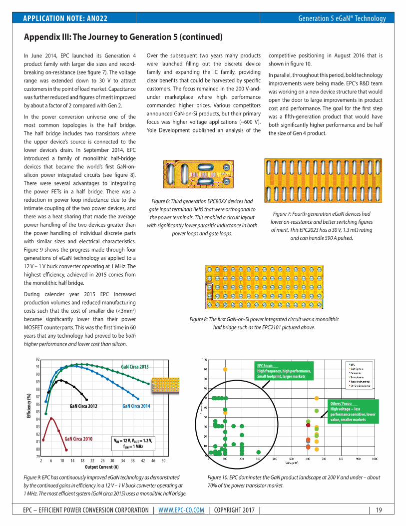
In the power conversion universe one of the most common topologies is the half bridge. The half bridge includes two transistors where the upper device’s source is connected to the lower device’s drain. In September 2014, EPC introduced a family of monolithic half-bridge devices that became the world’s first GaN-on-silicon power integrated circuits (see figure 8). There were several advantages to integrating the power FETs in a half bridge. There was a reduction in power loop inductance due to the intimate coupling of the two power devices, and there was a heat sharing that made the average power handling of the two devices greater than the power handling of individual discrete parts with similar sizes and electrical characteristics. Figure 9 shows the progress made through four generations of eGaN technology as applied to a 12 V – 1 V buck converter operating at 1 MHz. The highest efficiency, achieved in 2015 comes from the monolithic half bridge.
During calender year 2015 EPC increased production volumes and reduced manufacturing costs such that the cost of smaller die (<3mm2) became significantly lower than their power MOSFET counterparts. This was the first time in 60 years that any technology had proved to be both higher performance and lower cost than silicon.
Appendix III: The Journey to Generation 5 (continued)
Figure 6: Third generation EPC80XX devices had gate input terminals (left) that were orthogonal to the power terminals. This enabled a circuit layout
with significantly lower parasitic inductance in both power loops and gate loops.
Figure 7: Fourth generation eGaN devices had lower on-resistance and better switching figures of merit. This EPC2023 has a 30 V, 1.3 mΩ rating
and can handle 590 A pulsed.
Figure 8: The first GaN-on-Si power integrated circuit was a monolithic half bridge such as the EPC2101 pictured above.
Figure 10: EPC dominates the GaN product landscape at 200 V and under – about 70% of the power transistor market.
Figure 9: EPC has continuously improved eGaN technology as demonstrated by the continued gains in efficiency in a 12 V – 1 V buck converter operating at 1 MHz. The most efficient system (GaN circa 2015) uses a monolithic half bridge.
GaN Circa 2014
GaN Circa 2010
GaN Circa 2012
GaN Circa 2015
VIN = 12 V, VOUT = 1.2 V,fSW = 1 MHz
2 6 10 30 34 38 42 46 5014 18 22 26
Ecie
ncy (
%)
Output Current (A)
92
91
90
89
88
87
86
85
84
83
82
81
80
79
EPC Focus:High frequency, high performance,Small footprint, larger markets
Others’ Focus:High voltage – lessperformance sensitive, lowervalue, smaller markets
Over the subsequent two years many products were launched filling out the discrete device family and expanding the IC family, providing clear benefits that could be harvested by specific customers. The focus remained in the 200 V-and-under marketplace where high performance commanded higher prices. Various competitors announced GaN-on-Si products, but their primary focus was higher voltage applications (~600 V). Yole Development published an analysis of the
competitive positioning in August 2016 that is shown in figure 10.
In parallel, throughout this period, bold technology improvements were being made. EPC’s R&D team was working on a new device structure that would open the door to large improvements in product cost and performance. The goal for the first step was a fifth-generation product that would have both significantly higher performance and be half the size of Gen 4 product.