
(focus on hybrid HgCdTe) - indico.bnl.gov · • Characterize contact resistance and its...
34
How well do we understand NIR detectors? (focus on hybrid HgCdTe) Roger Smith Caltech 2018-12-03
Transcript of (focus on hybrid HgCdTe) - indico.bnl.gov · • Characterize contact resistance and its...

How well do we understand NIR detectors? (focus on hybrid HgCdTe)
Roger Smith
Caltech 2018-12-03
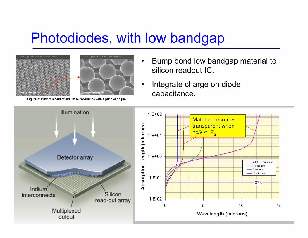
Photodiodes, with low bandgap • Bump bond low bandgap material to
silicon readout IC.
• Integrate charge on diode capacitance.
Material becomes transparent when hc/λ < Eg
SPIE 7021-22, Marseille 2008-06-24
Roger Smith et al., Caltech
3
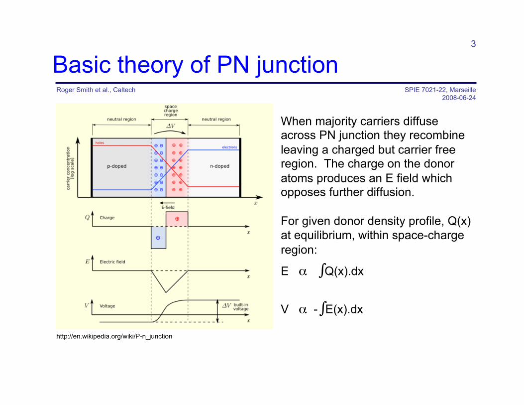
Basic theory of PN junction
• When majority carriers diffuse across PN junction they recombine leaving a charged but carrier free region. The charge on the donor atoms produces an E field which opposes further diffusion.
• For given donor density profile, Q(x) at equilibrium, within space-charge region:
• E α ∫Q(x).dx
• V α - ∫E(x).dx
http://en.wikipedia.org/wiki/P-n_junction
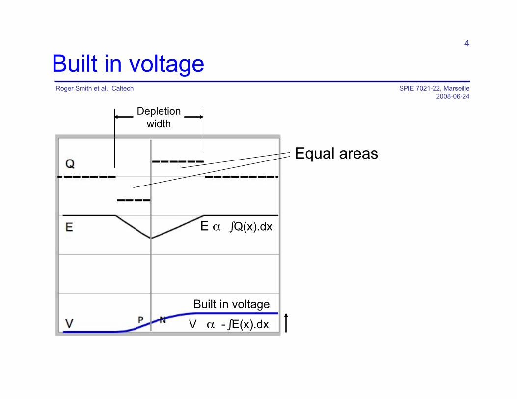
Depletion width
Built in voltage
E α ∫Q(x).dx
V α - ∫E(x).dx
SPIE 7021-22, Marseille 2008-06-24
Roger Smith et al., Caltech
4
Built in voltage
Equal areas
SPIE 7021-22, Marseille 2008-06-24
Roger Smith et al., Caltech
5
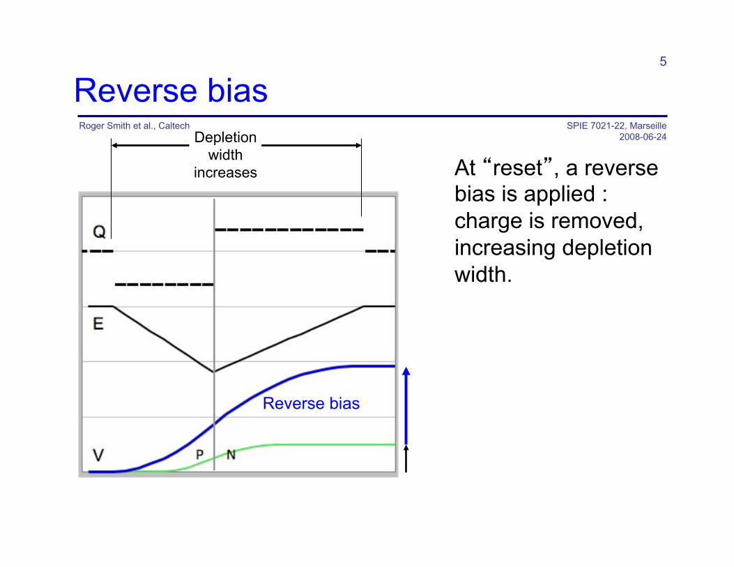
Reverse bias
At “reset”, a reverse bias is applied : charge is removed, increasing depletion width.
Built in voltage
Depletion width
increases
Reverse bias
SPIE 7021-22, Marseille 2008-06-24
Roger Smith et al., Caltech
6
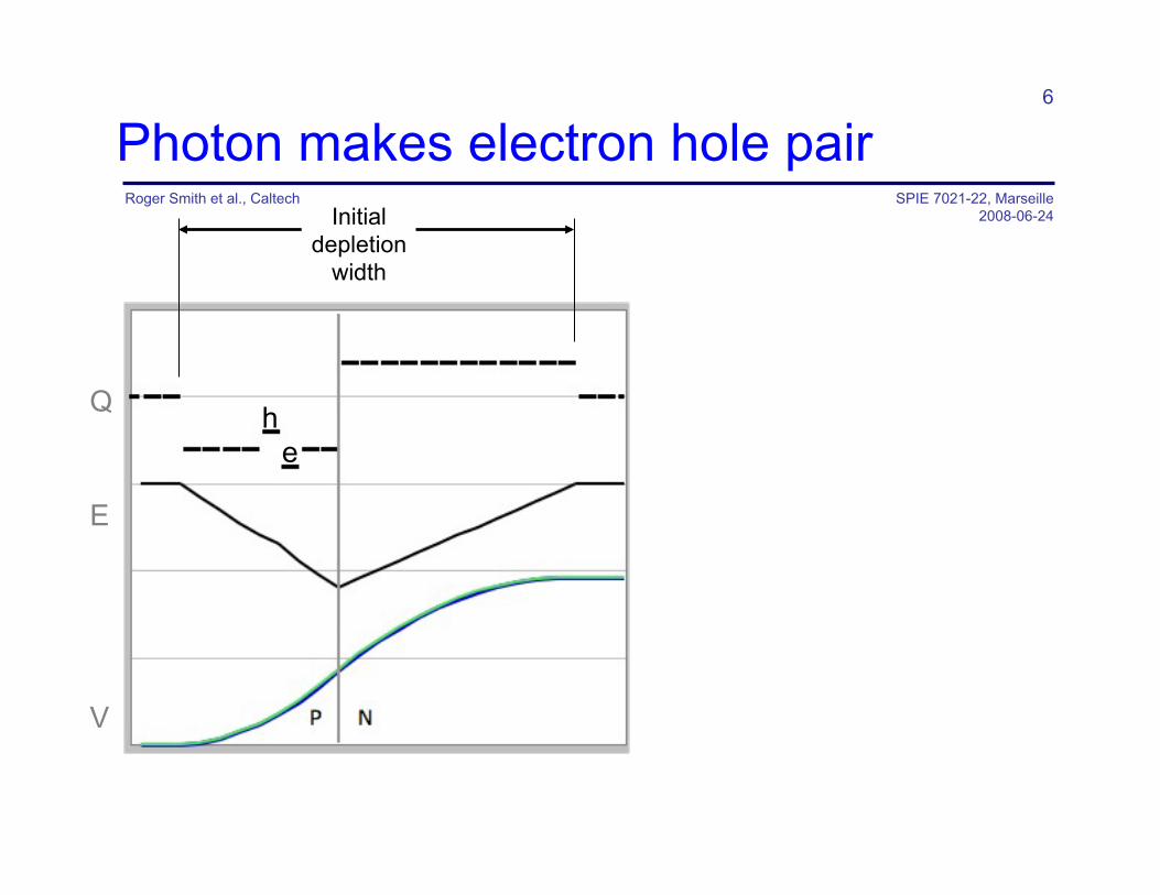
Photon makes electron hole pair
Q
E
V
Initial depletion
width
he
SPIE 7021-22, Marseille 2008-06-24
Roger Smith et al., Caltech
7
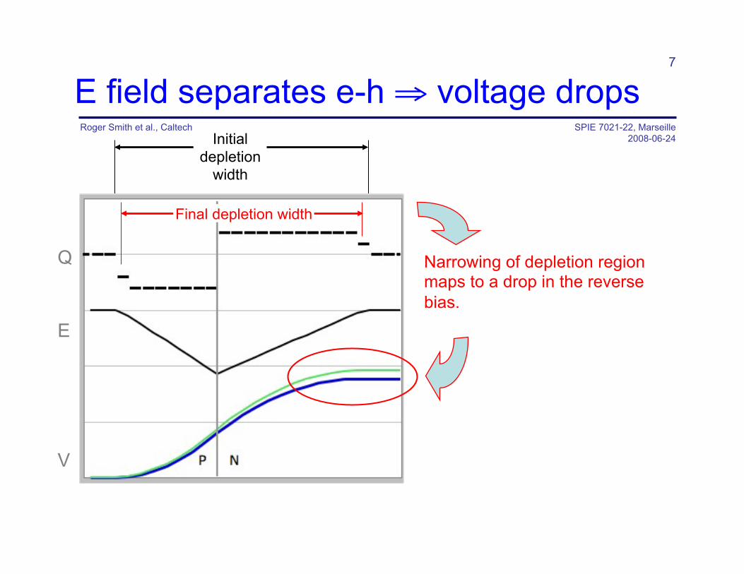
E field separates e-h ⇒ voltage drops
Q
E
V
Initial depletion
width
Final depletion width
Narrowing of depletion region maps to a drop in the reverse bias.
SPIE 7021-22, Marseille 2008-06-24
Roger Smith et al., Caltech
8
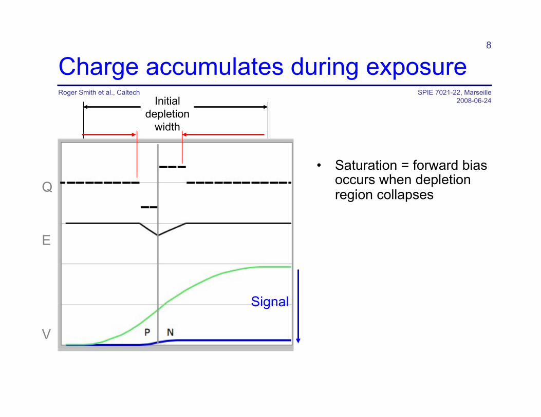
Charge accumulates during exposure
• Saturation = forward bias occurs when depletion region collapses Q
E
V
Initial depletion
width
he
he
he
he
he
he
he
he
he
he
he
he
he
he
he
he
he
he
Signal

SPIE 7021-22, Marseille 2008-06-24
Roger Smith et al., Caltech
9
PN junctions on common substrate
Silicon Multiplexor ~ 600µm thick
Undepleted Dsub (N)
Depleted N-type
Depleted P-type
CdZnTe substrate is fully removed
Undepleted implant (P)
HgCdTe
Indium bump bonds
~3µm ?
18µm
Epoxy wicked into voids between bumps prior to substrate removal
Silicon Carbide or Molybdenum package Epoxy

SPIE 7021-22, Marseille 2008-06-24
Roger Smith et al., Caltech
10
PN junctions on common substrate
Silicon Multiplexor ~ 600µm thick
Undepleted Dsub (N)
Depleted N-type
Depleted P-type
Undepleted implant (P)
HgCdTe
18µm
Epoxy wicked into voids between bumps prior to substrate removal
Silicon Carbide or Molybdenum package Epoxy
Dielectric
Areas with mobile carriers act as capacitor plates

SPIE 7021-22, Marseille 2008-06-24
Roger Smith et al., Caltech
11
Inter-Pixel Capacitance
Silicon Multiplexor ~ 600µm thick
HgCdTe Dielectric constant of epoxy underfill increases IPC
Silicon Carbide or Molybdenum package
Depletion region is dielectric: More signal (or lower bias) à Higher capacitance à = non-linear
Conductive substrate shields pixel from its neighbors
SPIE 7021-22, Marseille 2008-06-24
Roger Smith et al., Caltech
12
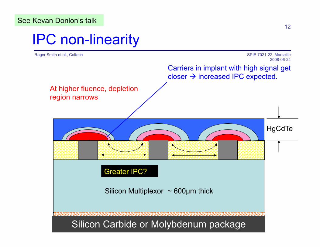
IPC non-linearity
Silicon Multiplexor ~ 600µm thick
HgCdTe
Silicon Carbide or Molybdenum package
At higher fluence, depletion region narrows
Carriers in implant with high signal get closer à increased IPC expected.
Greater IPC?
See Kevan Donlon’s talk
Silicon Multiplexor ~ 600µm thick
HgCdTe
SPIE 7021-22, Marseille 2008-06-24
Roger Smith et al., Caltech
13
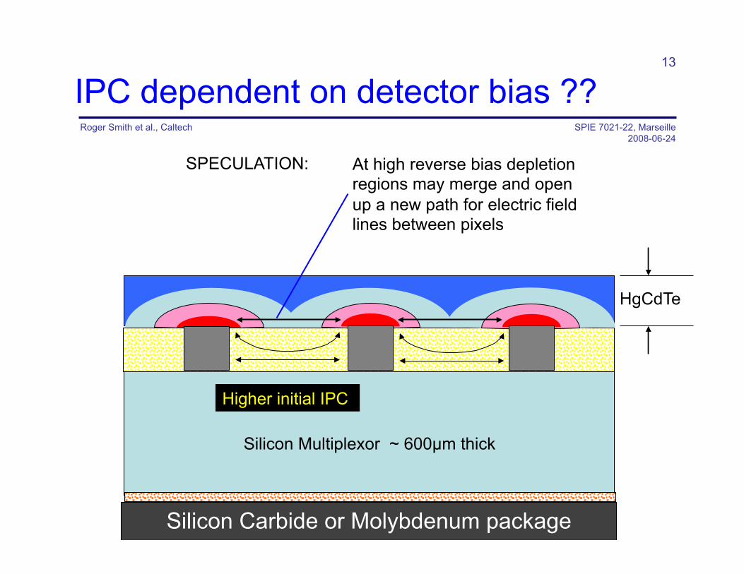
IPC dependent on detector bias ??
Silicon Carbide or Molybdenum package
Higher initial IPC
At high reverse bias depletion regions may merge and open up a new path for electric field lines between pixels
SPECULATION:

SPIE 7021-22, Marseille 2008-06-24
Roger Smith et al., Caltech
14
Pixel boundaries after reset
Silicon Multiplexor ~ 600µm thick
HgCdTe
Silicon Carbide or Molybdenum package

SPIE 7021-22, Marseille 2008-06-24
Roger Smith et al., Caltech
15
Signal contrast moves boundary
Silicon Multiplexor ~ 600µm thick
HgCdTe
Silicon Carbide or Molybdenum package
Pixel shrinks as charge accumulates so PSF seems to grow.
Brighter-fatter paper by Andres Plazas; see Eric Huff’s talk
Depleted
Mobile holes
Mobile electrons
- - -
+ + +
- - -
- -
+ + +
+ +
Signal (lower bias)
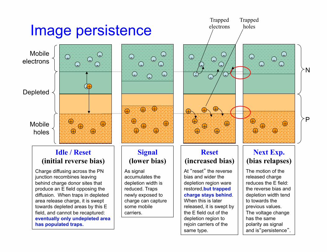
As signal accumulates the depletion width is reduced. Traps newly exposed to charge can capture some mobile carriers.
Image persistence
+ + +
+ +
- - -
- -
Idle / Reset (initial reverse bias)
Charge diffusing across the PN junction recombines leaving behind charge donor sites that produce an E field opposing the diffusion. When traps in depleted area release charge, it is swept towards depleted areas by this E field, and cannot be recaptured: eventually only undepleted area has populated traps.
P
N-
- - -
-
+ + +
+ +
Next Exp. (bias relapses) The motion of the released charge reduces the E field: the reverse bias and depletion width tend to towards the previous values. The voltage change has the same polarity as signal and is“persistence”.
Trapped holes
Trapped electrons
- - -
+ + +
+ + +
+ +
- - -
- -
Reset (increased bias) At “reset” the reverse bias and wider the depletion region ware restored,but trapped charge stays behind. When this is later released, it is swept by the E field out of the depletion region to rejoin carriers of the same type.
- +
SPIE 7021-22, Marseille 2008-06-24
Roger Smith et al., Caltech
17
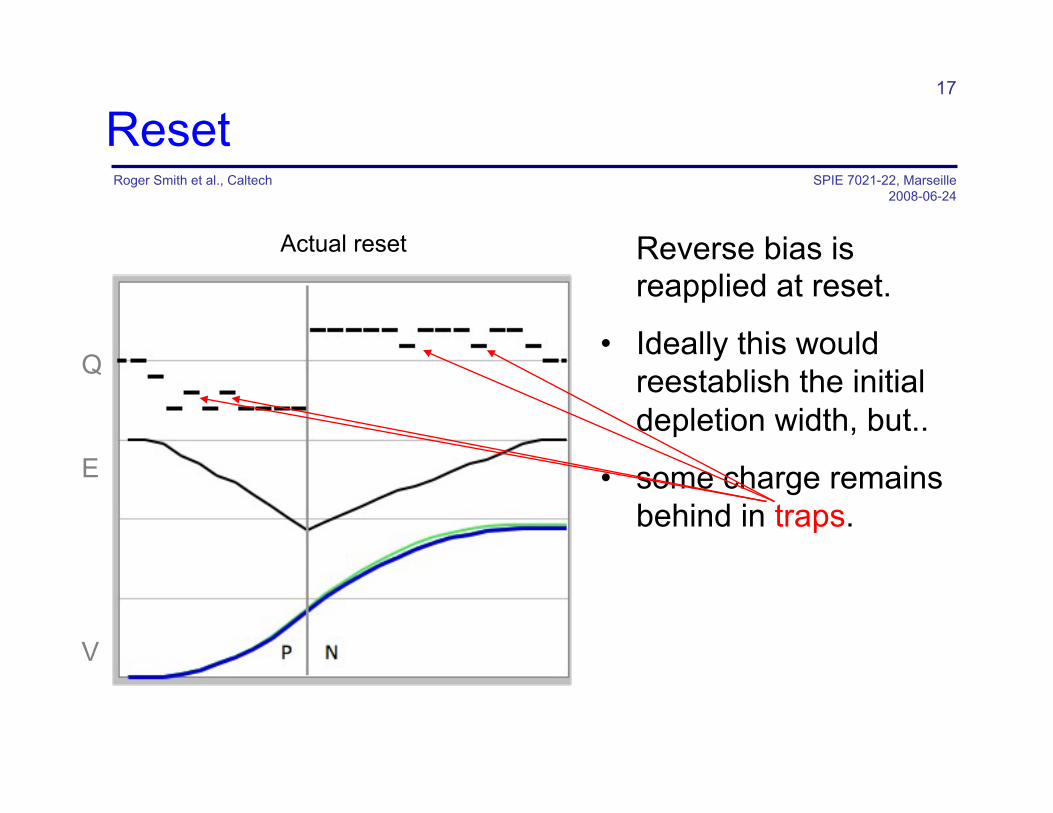
Reset
Reverse bias is reapplied at reset.
• Ideally this would reestablish the initial depletion width, but..
• some charge remains behind in traps.
Q
E
V
Before Reset Ideal Reset Actual reset
SPIE 7021-22, Marseille 2008-06-24
Roger Smith et al., Caltech
18
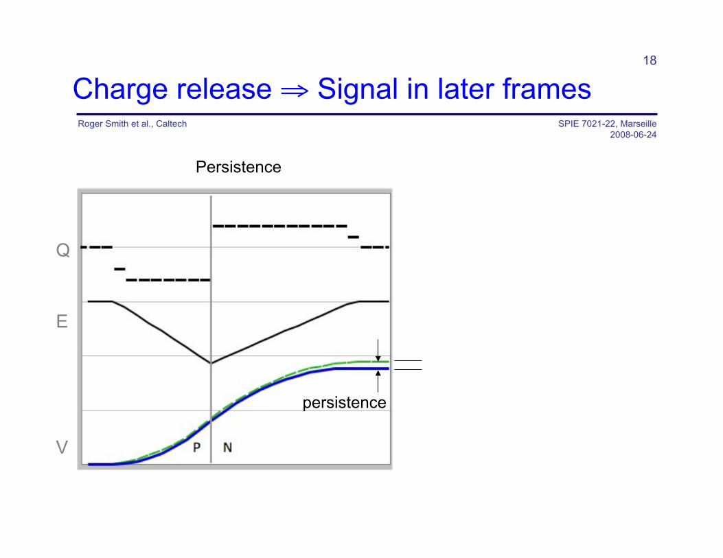
Charge release ⇒ Signal in later frames
Q
E
V
persistence
Persistence
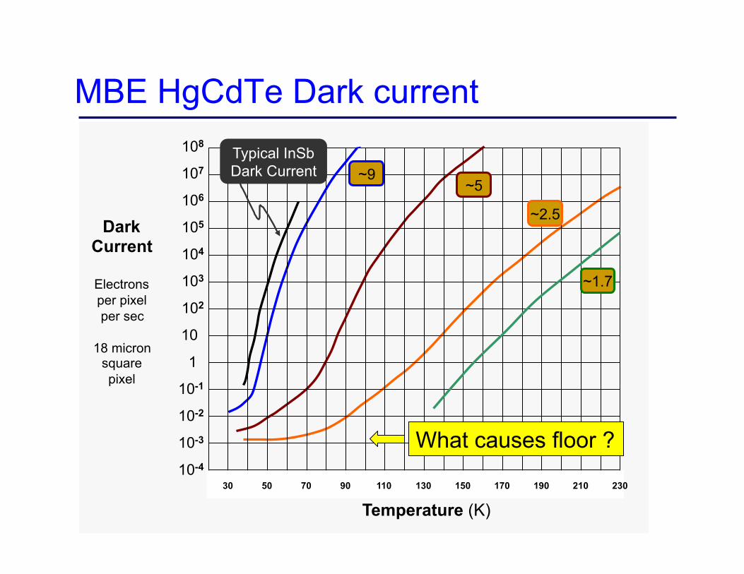
MBE HgCdTe Dark current
~9 ~5
~2.5
~1.7
Typical InSb Dark Current
108
107
106
105
104
103
102
10
1
10-2
10-3
10-4
230 210 190 170 150 130 110 90 70 50 30
Temperature (K)
Dark Current
Electrons per pixel per sec
18 micron
square pixel
10-1
What causes floor ?
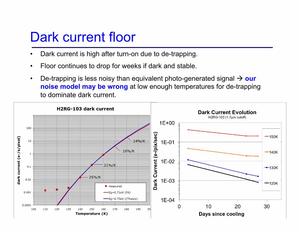
Dark current floor • Dark current is high after turn-on due to de-trapping.
• Floor continues to drop for weeks if dark and stable.
• De-trapping is less noisy than equivalent photo-generated signal à our noise model may be wrong at low enough temperatures for de-trapping to dominate dark current.
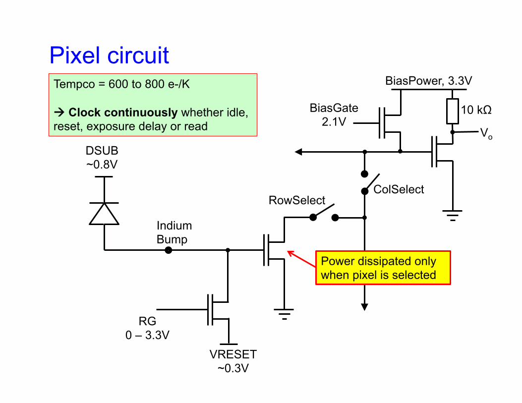
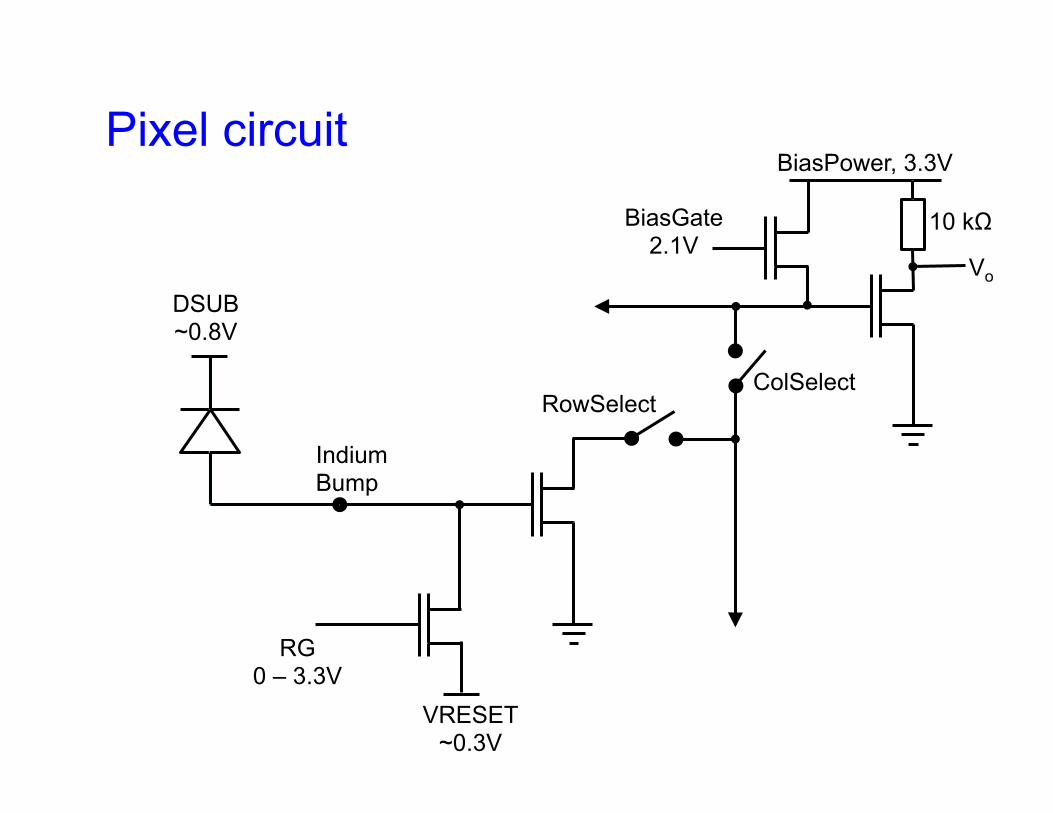
Pixel circuit
DSUB ~0.8V
VRESET ~0.3V
RG 0 – 3.3V
Vo
BiasGate 2.1V
RowSelect ColSelect
Indium Bump
Power dissipated only when pixel is selected
Tempco = 600 to 800 e-/K à Clock continuously whether idle, reset, exposure delay or read
BiasPower, 3.3V
10 kΩ
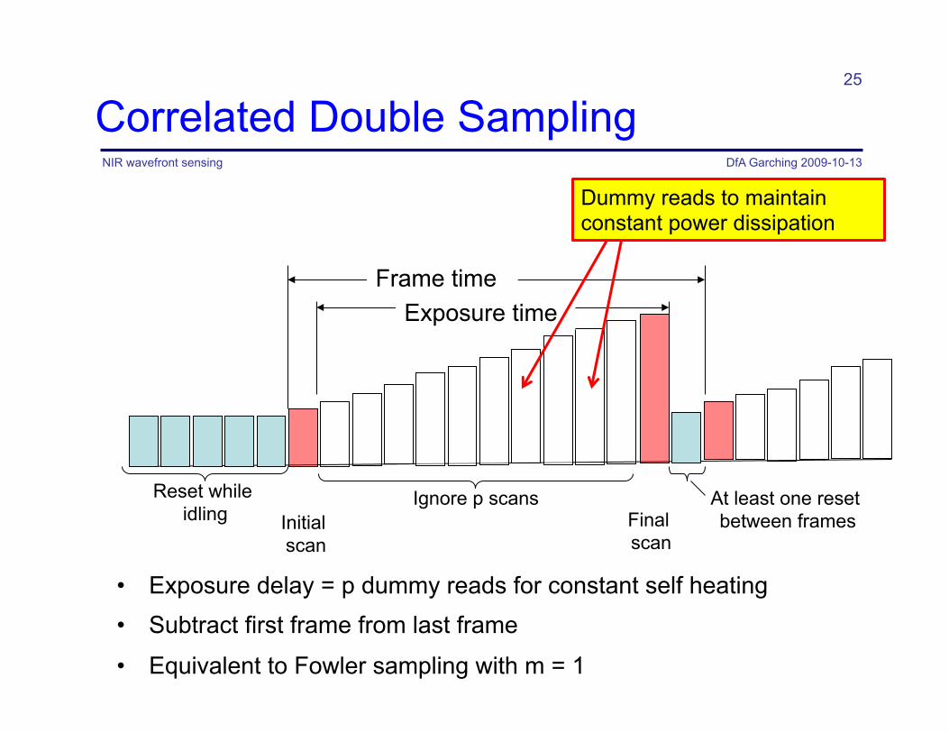
Correlated Double Sampling
• Exposure delay = p dummy reads for constant self heating • Subtract first frame from last frame
• Equivalent to Fowler sampling with m = 1
DfA Garching 2009-10-13 NIR wavefront sensing
25
Ignore p scans At least one reset between frames
Reset while idling Initial
scan Final scan
Exposure time Frame time
Dummy reads to maintain constant power dissipation
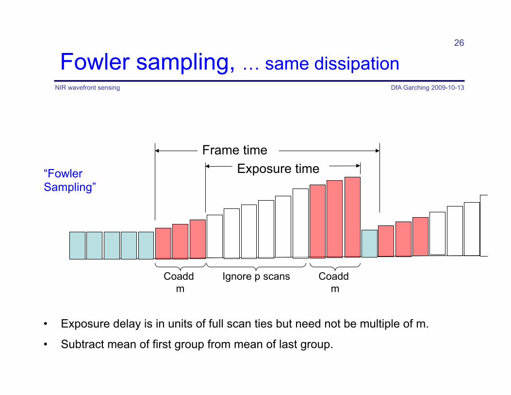
Fowler sampling, … same dissipation
• Exposure delay is in units of full scan ties but need not be multiple of m.
• Subtract mean of first group from mean of last group.
DfA Garching 2009-10-13 NIR wavefront sensing
26
Coadd m
Ignore p scans Coadd m
Exposure time Frame time
“Fowler Sampling”
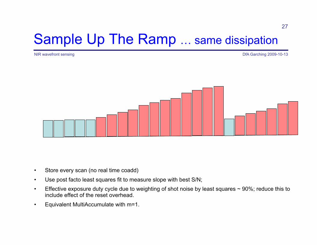
Sample Up The Ramp … same dissipation
• Store every scan (no real time coadd)
• Use post facto least squares fit to measure slope with best S/N; • Effective exposure duty cycle due to weighting of shot noise by least squares ~ 90%; reduce this to
include effect of the reset overhead.
• Equivalent MultiAccumulate with m=1.
DfA Garching 2009-10-13 NIR wavefront sensing
27
DSUB ~0.8V
VRESET ~0.3V
RG 0 – 3.3V
Vo
BiasGate 2.1V
RowSelect ColSelect
Indium Bump
Pixel circuit BiasPower, 3.3V
10 kΩ
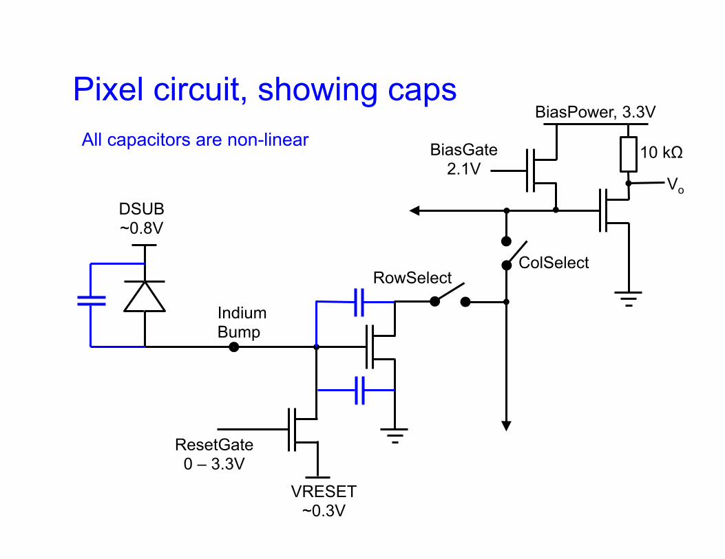
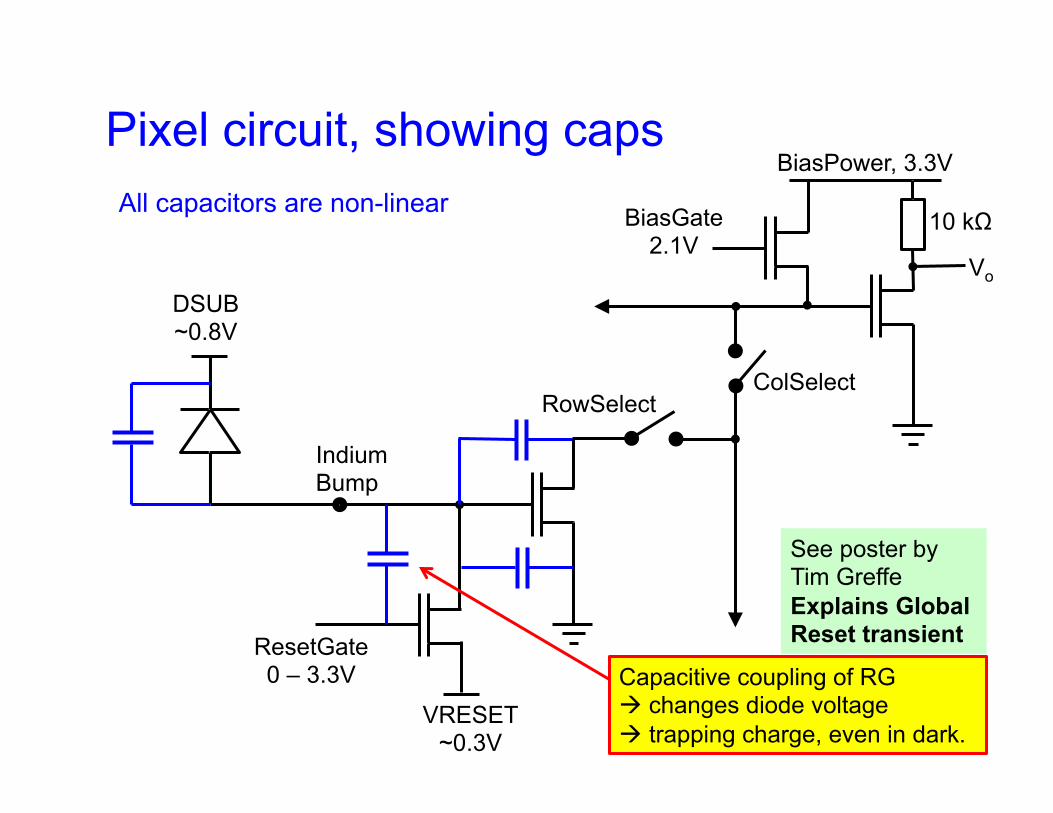
Pixel circuit, showing caps
DSUB ~0.8V
VRESET ~0.3V
ResetGate 0 – 3.3V
Vo
BiasGate 2.1V
RowSelect ColSelect
Indium Bump
All capacitors are non-linear BiasPower, 3.3V
10 kΩ
Pixel circuit, showing caps
DSUB ~0.8V
VRESET ~0.3V
ResetGate 0 – 3.3V
Vo
BiasGate 2.1V
RowSelect ColSelect
Indium Bump
All capacitors are non-linear
Capacitive coupling of RG à changes diode voltage à trapping charge, even in dark.
See poster by Tim Greffe Explains Global Reset transient
10 kΩ
BiasPower, 3.3V
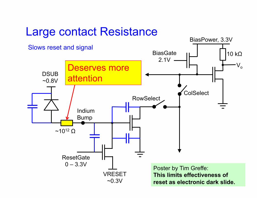
Large contact Resistance
DSUB ~0.8V
VRESET ~0.3V
ResetGate 0 – 3.3V
BiasPower, 3.3V
Vo
BiasGate 2.1V
RowSelect ColSelect
Indium Bump
Slows reset and signal
Poster by Tim Greffe: This limits effectiveness of reset as electronic dark slide.
Deserves more attention
~1012 Ω
10 kΩ
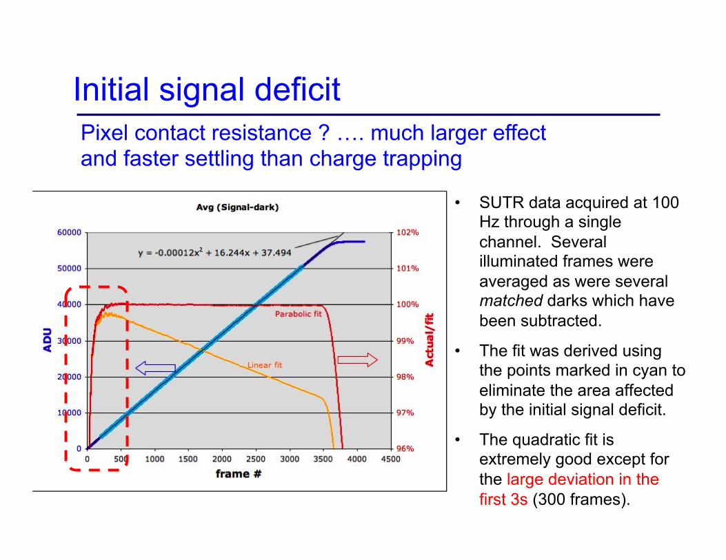
Initial signal deficit
• SUTR data acquired at 100 Hz through a single channel. Several illuminated frames were averaged as were several matched darks which have been subtracted.
• The fit was derived using the points marked in cyan to eliminate the area affected by the initial signal deficit.
• The quadratic fit is extremely good except for the large deviation in the first 3s (300 frames).
Pixel contact resistance ? …. much larger effect and faster settling than charge trapping
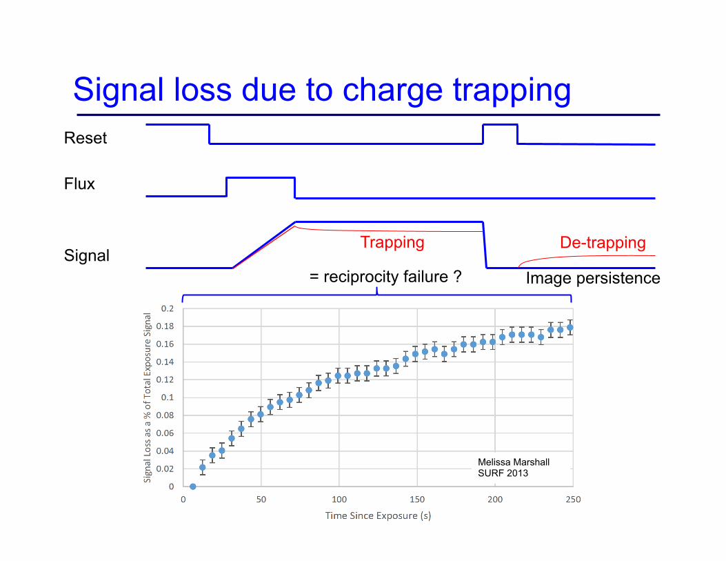
Signal loss due to charge trapping
Flux
Reset
Signal Trapping De-trapping
Image persistence = reciprocity failure ?
Melissa Marshall SURF 2013
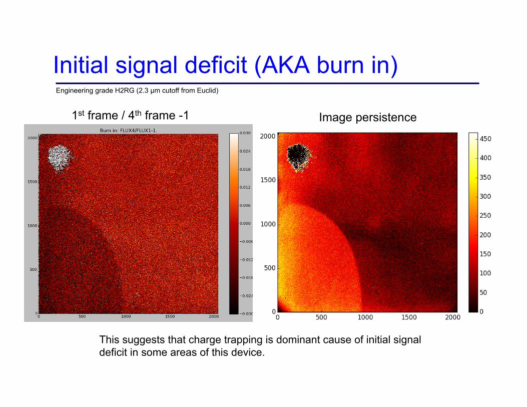
Initial signal deficit (AKA burn in)
1st frame / 4th frame -1 Image persistence
Engineering grade H2RG (2.3 µm cutoff from Euclid)
This suggests that charge trapping is dominant cause of initial signal deficit in some areas of this device.
Read noise
• The photodiodes generate more read noise than the ROIC and have much stronger 1/f component, as demonstrated by much lower noise and better reduction by multiple sampling for à Permanent reset (shorting out detector noise) à Reference pixels
• Is this due to trapping/detrapping?
• Contact resistance is about the correct magnitude to produce about this much Johnson noise. • This is worth investigating since lower contact resistance could
improve both dynamics (linearity) and noise.
Linearity
• First, subtract time-dependent offsets – Self heating (minimize by Constant Cadence Clocking) – Electronic drifts (reference pixels help) – Reset induced (de)trapping
• Correct for dependence of capacitance on voltage
• Correct for trapping of charge (complicated)
• Correct for photodiode time-constant (contact resistance)
Everything is spatially variable.
Rarely is this well characterized and corrected
See Bernie Rauscher’s talk
To do list
• Characterize contact resistance and its consequences
• Study burn-in and reciprocity failure to see how much comes from contact resistance an how much from trapping.
• Evaluate noise produced by dark current at floor. Hot pixels may be noisier.
• Improve linearity calibration methods and/or fix these odd behaviors which make linearity correction so difficult.