Flash Light Millisecond Self‐Assembly of High χ Block …fand.kaist.ac.kr/Attach/AM -...
7
COMMUNICATION 1700595 (1 of 7) © 2017 WILEY-VCH Verlag GmbH & Co. KGaA, Weinheim www.advmat.de Flash Light Millisecond Self-Assembly of High χ Block Copolymers for Wafer-Scale Sub-10 nm Nanopatterning Hyeong Min Jin, Dae Yong Park, Seong-Jun Jeong, Gil Yong Lee, Ju Young Kim, Jeong Ho Mun, Seung Keun Cha, Joonwon Lim, Jun Soo Kim, Kwang Ho Kim,* Keon Jae Lee,* and Sang Ouk Kim* Dr. H. M. Jin, G. Y. Lee, Dr. J. Y. Kim, Dr. J. H. Mun, S. K. Cha, Dr. J. Lim, J. S. Kim, Prof. S. O. Kim National Creative Research Initiative Center for Multi-Dimensional Directed Nanoscale Assembly Department of Materials Science and Engineering KAIST Daejeon 34141, Republic of Korea E-mail: [email protected] D. Y. Park, Prof. K. J. Lee Department of Materials Science and Engineering KAIST Daejeon 34141, Republic of Korea E-mail: [email protected] Dr. S.-J. Jeong Device Laboratory Device & System Research Center Samsung Advanced Institute and Technology Suwon 16678, Republic of Korea Prof. K. H. Kim Department of Materials Science and Engineering Pusan National University Pusan 46241, Republic of Korea E-mail: [email protected] DOI: 10.1002/adma.201700595 Directed self-assembly (DSA) of block copolymers (BCPs) [1] is a promising nano- patterning technology that can address the inherent limitations of conventional photolithography. [2,3] Recently, BCPs with high Flory–Huggins interaction parameter (χ) have been extensively explored for the nanoscale patterning with critical dimen- sions approaching the thermodynamic theoretical limit of BCP self-assembly (≈3 nm). Unfortunately, topological defect annihilation of high-χ BCPs is generally difficult compared to low-χ counterparts due to the strong interblock segregation, which leads to a retarded diffusion of polymer chains across microphase sepa- rated distinct nanodomains. [4] Moreover, generic high order–disorder transition temperatures (T ODT ) of the high-χ BCPs, typically above their thermal degradation temperatures, commonly prevent typical thermal annealing processes from being used in a high ordered self-assembly in a reasonable time scale. [5] Instead, a variety of solvent vapor treatment methods, such as solvo- thermal, [6] solvo-microwave annealing, [7] and worm-spin casting methods, [8] have been proposed to enhance the chain diffusivity of high-χ BCPs by temporally reducing the χ values through solvent dilution. [9] Nonetheless, difficult controllability of the solvent vapor pressure over a large wafer-scale area as well as other practical issues, including easy dewetting of solvent swollen BCP films, commonly makes it hard to employ these approaches for viable device manufacture process. Photothermal process that converts photon energy into thermal energy has been recently actively investigated for the ultrafast high temperature annealing of organic, [10] inorganic, [11] and hybrid materials [12] with enormous advantages, such as rapid processing and minimal influence on neighboring struc- tures with low thermal stabilities. Notably, several research groups including us, reported the directed self-assembly of BCPs using laser beams as a light source for photothermal annealing. [13] Despite the unique advantages including area- selective patternability, laser process has a critical drawback for the large-area manufacture level process owing to the small size and spatial energy variation of focused spot laser beam. In this work, we introduce large-area flash light triggered millisecond level ultrafast self-assembly of high-χ BCP thin One of the fundamental challenges encountered in successful incorpora- tion of directed self-assembly in sub-10 nm scale practical nanolithography is the process compatibility of block copolymers with a high Flory–Huggins interaction parameter (χ). Herein, reliable, fab-compatible, and ultrafast directed self-assembly of high-χ block copolymers is achieved with intense flash light. The instantaneous heating/quenching process over an extremely high temperature (over 600 °C) by flash light irradiation enables large grain growth of sub-10 nm scale self-assembled nanopatterns without thermal degradation or dewetting in a millisecond time scale. A rapid self-assembly mechanism for a highly ordered morphology is identified based on the kinetics and thermodynamics of the block copolymers with strong segrega- tion. Furthermore, this novel self-assembly mechanism is combined with graphoepitaxy to demonstrate the feasibility of ultrafast directed self- assembly of sub-10 nm nanopatterns over a large area. A chemically modi- fied graphene film is used as a flexible and conformal light-absorbing layer. Subsequently, transparent and mechanically flexible nanolithography with a millisecond photothermal process is achieved leading the way for roll-to-roll processability. Nanopatterning Adv. Mater. 2017, 29, 1700595
Transcript of Flash Light Millisecond Self‐Assembly of High χ Block …fand.kaist.ac.kr/Attach/AM -...
CommuniCation
1700595 (1 of 7) © 2017 WILEY-VCH Verlag GmbH & Co. KGaA, Weinheim
www.advmat.de
Flash Light Millisecond Self-Assembly of High χ Block Copolymers for Wafer-Scale Sub-10 nm Nanopatterning
Hyeong Min Jin, Dae Yong Park, Seong-Jun Jeong, Gil Yong Lee, Ju Young Kim, Jeong Ho Mun, Seung Keun Cha, Joonwon Lim, Jun Soo Kim, Kwang Ho Kim,* Keon Jae Lee,* and Sang Ouk Kim*
Dr. H. M. Jin, G. Y. Lee, Dr. J. Y. Kim, Dr. J. H. Mun, S. K. Cha, Dr. J. Lim, J. S. Kim, Prof. S. O. KimNational Creative Research Initiative Center for Multi-Dimensional Directed Nanoscale AssemblyDepartment of Materials Science and EngineeringKAISTDaejeon 34141, Republic of KoreaE-mail: [email protected]. Y. Park, Prof. K. J. LeeDepartment of Materials Science and EngineeringKAISTDaejeon 34141, Republic of KoreaE-mail: [email protected]. S.-J. JeongDevice LaboratoryDevice & System Research CenterSamsung Advanced Institute and TechnologySuwon 16678, Republic of KoreaProf. K. H. KimDepartment of Materials Science and EngineeringPusan National UniversityPusan 46241, Republic of KoreaE-mail: [email protected]
DOI: 10.1002/adma.201700595
Directed self-assembly (DSA) of block copolymers (BCPs)[1] is a promising nano-patterning technology that can address the inherent limitations of conventional photolithography.[2,3] Recently, BCPs with high Flory–Huggins interaction parameter (χ) have been extensively explored for the nanoscale patterning with critical dimen-sions approaching the thermodynamic theoretical limit of BCP self-assembly (≈3 nm). Unfortunately, topological defect annihilation of high-χ BCPs is generally difficult compared to low-χ counterparts due to the strong interblock segregation, which leads to a retarded diffusion of polymer chains across microphase sepa-rated distinct nanodomains.[4] Moreover, generic high order–disorder transition temperatures (TODT) of the high-χ BCPs, typically above their thermal degradation temperatures, commonly prevent typical thermal annealing processes from being used in a high ordered self-assembly in a reasonable time scale.[5] Instead, a
variety of solvent vapor treatment methods, such as solvo-thermal,[6] solvo-microwave annealing,[7] and worm-spin casting methods,[8] have been proposed to enhance the chain diffusivity of high-χ BCPs by temporally reducing the χ values through solvent dilution.[9] Nonetheless, difficult controllability of the solvent vapor pressure over a large wafer-scale area as well as other practical issues, including easy dewetting of solvent swollen BCP films, commonly makes it hard to employ these approaches for viable device manufacture process.
Photothermal process that converts photon energy into thermal energy has been recently actively investigated for the ultrafast high temperature annealing of organic,[10] inorganic,[11] and hybrid materials[12] with enormous advantages, such as rapid processing and minimal influence on neighboring struc-tures with low thermal stabilities. Notably, several research groups including us, reported the directed self-assembly of BCPs using laser beams as a light source for photothermal annealing.[13] Despite the unique advantages including area-selective patternability, laser process has a critical drawback for the large-area manufacture level process owing to the small size and spatial energy variation of focused spot laser beam.
In this work, we introduce large-area flash light triggered millisecond level ultrafast self-assembly of high-χ BCP thin
One of the fundamental challenges encountered in successful incorpora-tion of directed self-assembly in sub-10 nm scale practical nanolithography is the process compatibility of block copolymers with a high Flory–Huggins interaction parameter (χ). Herein, reliable, fab-compatible, and ultrafast directed self-assembly of high-χ block copolymers is achieved with intense flash light. The instantaneous heating/quenching process over an extremely high temperature (over 600 °C) by flash light irradiation enables large grain growth of sub-10 nm scale self-assembled nanopatterns without thermal degradation or dewetting in a millisecond time scale. A rapid self-assembly mechanism for a highly ordered morphology is identified based on the kinetics and thermodynamics of the block copolymers with strong segrega-tion. Furthermore, this novel self-assembly mechanism is combined with graphoepitaxy to demonstrate the feasibility of ultrafast directed self-assembly of sub-10 nm nanopatterns over a large area. A chemically modi-fied graphene film is used as a flexible and conformal light-absorbing layer. Subsequently, transparent and mechanically flexible nanolithography with a millisecond photothermal process is achieved leading the way for roll-to-roll processability.
Nanopatterning
Adv. Mater. 2017, 29, 1700595
© 2017 WILEY-VCH Verlag GmbH & Co. KGaA, Weinheim1700595 (2 of 7)
www.advmat.dewww.advancedsciencenews.com
films. We utilize achromatic incoherent light from a xenon flash lamp (broad spectrum from UV to near infrared (NIR), the highest intensity in NIR region) as a light source for photo-thermal annealing of high-χ BCPs over a wafer-scale large area. Compared to the widely used conventional camera flash, xenon flash lamp system has an advantage of precisely adjust-able output power and pulse duration. Xenon flash lamp is also attractive for its large area processability over a wafer scale and compatibility with roll-to-roll continuous process systems.[14] Large-area instantaneous heating/quenching over a high tem-perature around 600 °C induced by intense flash light enables the effective high order self-assembly of high-χ BCP films near the TODT without noticeable thermal degradation under atmos-pheric conditions. We also present successful graphoepitaxy
of high-χ BCP self-assembly with only a single shot of flash light, demonstrating the feasibility for sub-10 nm scale DSA nanopatterning.
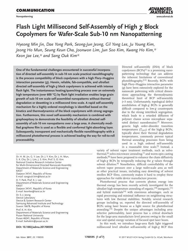
Figure 1a shows a schematic illustration of the millisecond ultrafast photothermal self-assembly based on flash light irra-diation. Pulsed irradiation of the flash light [duration (full width at half maximum, FWHM): 15 ms] onto the BCP thin films deposited on a silicon substrate generates effective self-assembly and grain growth of the BCPs. This rapid assembly can be achieved by extremely high temperature (peak tempera-ture, Tpeak ≈ 600 °C) annealing within a millisecond duration enabled by the intensive photothermal effect from flash light. Finite element method (FEM) analysis of the photothermal effect [average energy density = 78.8 J cm−2 and light pulse
Adv. Mater. 2017, 29, 1700595
Figure 1. Millisecond flash lamp annealing (FLA) of a BCP self-assembly. a) Schematic illustration of FLA for BCP self-assembly. b) Numerical calcu-lated temperature profile and c) temperature distribution during FLA (at 12 ms). The inset of (b) shows the wavelength distribution of xenon flash lamp. Self-assembled morphologies of high-χ d) SD16, e) SD25, f) S4V16 and low-χ g) SM53.5 and h) S2V33. Top row (d)–(h) shows the structures from conventional thermal annealing (250 °C, 500 s), while bottom row corresponds to the structures from FLA (78.8 J cm−2, 1 time).
© 2017 WILEY-VCH Verlag GmbH & Co. KGaA, Weinheim1700595 (3 of 7)
www.advmat.dewww.advancedsciencenews.com
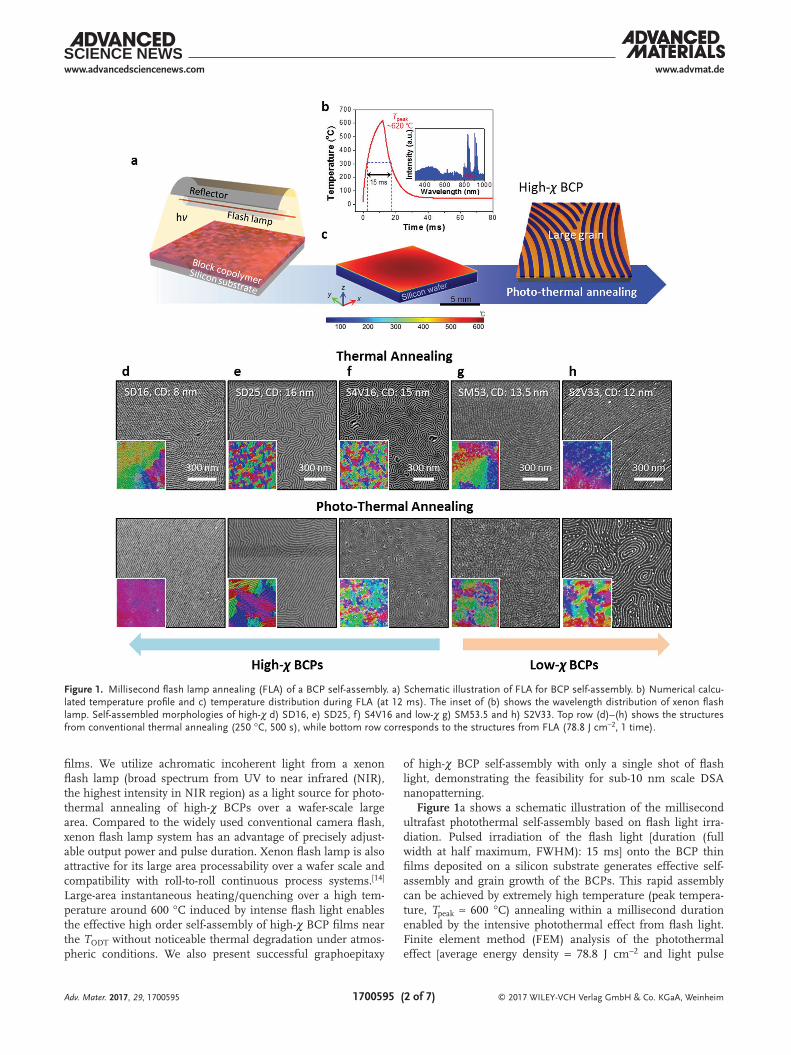
duration (FWHM): 15 ms] at the silicon substrate are shown in Figure 1b,c.[15] Owing to the 2D large area processability of our xenon flash lamp system, the temperature of large surface area of silicon substrate (10 mm × 10 mm) uniformly reaches over 600 °C (Figures S1–S3, Supporting Information). A representa-tive surface temperature profile at silicon substrate is shown in Figure 1b. Within 12 ms immediately after the flash light irra-diation, the surface temperature of silicon substrate increases rapidly up to 620 °C and then quenches below the glass transi-tion temperature (Tg) of BCPs within a few tens of milliseconds. Particularly, this flash lamp annealing (FLA) process is effective for high-χ PS-b-PDMS (SD, χ25 °C: 0.27) and PS-b-P4VP (S4V, χ25 °C: 0.53) BCPs (Table 1).
The self-assembled morphologies of BCPs induced by flash light (78.8 J cm−2; 1 pulse in air) and conventional thermal (250 °C; 500 s in N2 atmosphere) annealing are compared in Figure 1d–h. For a better legibility of pattern ordering, orien-tation mappings are displayed as inset in each panel of scan-ning electron microscope (SEM) image. High-χ SD BCPs with molecular weight (Mn) of 16 kg mol−1 (SD16) show the typical in-plane cylinder pattern with numerous disclinations by conventional thermal annealing (Figure 1d, top). By con-trast, extremely large grain with few disclinations is observed with only a single shot of flash light (Figure 1d, bottom). FLA induces ≈33 300 times faster self-assembly behavior than con-ventional thermal process; besides, a higher ordered mor-phology is formed. Likewise, cylinder forming SD25 and S4V BCPs with Mn of 16 kg mol−1 (S4V16) shows a similar tendency that much larger grain growth occurred under FLA compared to conventional thermal annealing (Figure 1e,f). Noticeably, a cylinder forming low-χ PS-b-PMMA (SM) BCPs with Mn of 53 kg mol−1 (SM53) and PS-b-P2VP (S2V) BCPs with Mn of 33 kg mol−1 reveals quite different results. As shown in Figure 1f,h, the self-assembled morphology formed by conven-tional thermal annealing shows larger grain growth than FLA.
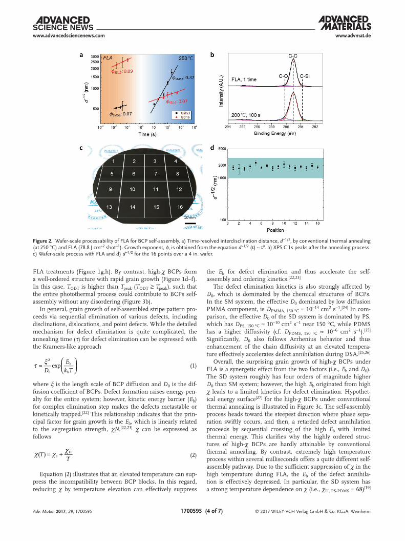
The average distance between the neighboring disclination cores of a stripe pattern can be approximated by d−1/2, where d is the areal defect density. This parameter can quantitatively represent the progression of grain growth. The d−1/2 for the self-assembled structures of high- (SD16) and low-χ (SM53) BCPs are calculated for the quantitative comparison of grain growth (Figure 2a).[20] The d−1/2 of FLA treated BCPs is plotted in the red area, whereas that of conventional thermal annealed BCPs (250 °C, N2 atmosphere) is in the blue region. For low-χ BCPs, FLA induces a much lower d−1/2 than thermal annealing.
Repeated FLA cycles do not give any noticeable morphology change (Figure S4, Supporting Information). By contrast, the high-χ BCPs show much higher d−1/2 values under FLA com-pared to thermal annealing. Obviously, rapid but extremely high-temperature process is more effective than long duration, moderate thermal process for the grain growth of high-χ BCPs.
Since FLA is a high-temperature process using achromatic broad wavelength irradiation under atmospheric condition, polymer degradation might be particularly concerned. In order to clarify this issue, BCP thin films were analyzed by X-ray photoelectron spectroscopy (XPS) after FLA process (Figure 2b and Figure S5, Supporting Information). Noteworthy that the CO peak (286.1 eV) of SD16 after FLA is even smaller than that after thermal process (200 °C, 100 s in air), verifying that the thermal degradation by FLA is insignificant in our experi-mental condition. SEM images of the BCP morphologies after multiple FLA treatments do not show any noticeable mor-phology degradation (Figure S4, Supporting Information). XPS analysis of SM56 after FLA also confirms that thermal degrada-tion is insignificant compared with conventional thermal pro-cess (Figure S5b, Supporting Information).
Wafer-scale large-area uniform processability of FLA is pre-sented in Figure 2c. Our home-made FLA system (Figure S3, Supporting Information) with a single lamp can radiate flash light over 2 cm × 2 cm area for the uniform heating over the entire surface (Figure 1c and Figure S6, Supporting Informa-tion). By means of a rapid sequential lateral scanning of FLA, BCP self-assembly was uniformly demonstrated over the whole area of 4 in. silicon wafer. The calculated d−1/2 at 16 points over the wafer have similar values near 2000 nm (1853 ± 318.9 nm) verifying that the BCP grains are evenly developed over the entire area (Figure 2d). Further scaling up to a manufacture level facilitation with a larger lamp or arrayed multiple flash lamps, possibly for continuous a roll-to-roll process system, should be highly anticipated.
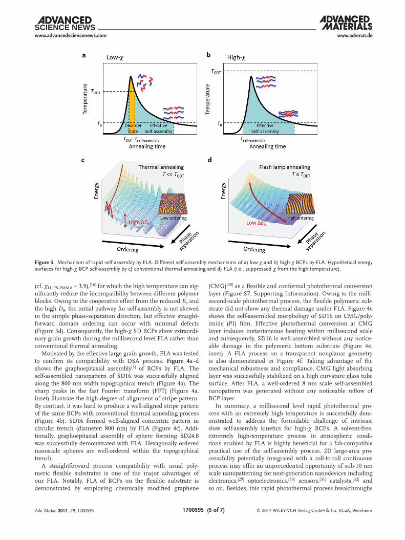
According to the χN values of BCPs, our FLA self-assembly leads to quite different behaviors, as summarized in Table 1. Figure 3a shows the self-assembly process of low-χ BCPs during FLA process. In this case, the TODT of BCP system is relatively low (TODT ≤ Tpeak) and thus BCPs undergo disordering or thermal fluctuation dominant behavior at T ≥ TODT (yellow region).[21] Effective self-assembly just starts when temperature reaches TODT during the cooling process (tself-assembly) and lasts until the melt is frozen (TODT > T > Tg). Thus, grain growth does not propagate effectively even with multiple repeated
Adv. Mater. 2017, 29, 1700595
Table 1. Properties of the BCPs of low-χ SM (PS-b-PMMA),[16] S2V (PS-b-P2VP),[17] and high-χ S4V (PS-b-P4VP)[18] and SD (PS-b-PDMS).[19] Effective-ness of FLA indicates the grain growth by FLA (78.8 J cm−2, 1 time) is faster compared to conventional thermal annealing (250 °C, 500 s).
BCP Pattern Classification of interaction parameter (χ)
Critical dimension [nm]
χ at 25 °C χN at 25 °C χN at 250 °C χN at 600 °C TODT [°C] Effectiveness of FLA
SM53 Cylinder Low-χ 13.5 0.04 21.1 18.2 16.6 ≈300 ×
S 2V33 Cylinder Low-χ 12 0.19 48.3 23.9 10.9 ≈360 ×
S 4V16 Cylinder High-χ 15 0.53 78.4 41.2 18.9 ≈600 ○
SD16 Cylinder High-χ 8 0.27 45.4 28.6 19.6 ≈700 ○
SD24.8 Sphere High-χ 12.5 0.27 66.6 41.9 28.8 >1000 ○
SD25 Cylinder High-χ 16 0.27 72.2 45.5 31.3 >2000 ○
© 2017 WILEY-VCH Verlag GmbH & Co. KGaA, Weinheim1700595 (4 of 7)
www.advmat.dewww.advancedsciencenews.com
FLA treatments (Figure 1g,h). By contrast, high-χ BCPs form a well-ordered structure with rapid grain growth (Figure 1d–f). In this case, TODT is higher than Tpeak (TODT ≥ Tpeak), such that the entire photothermal process could contribute to BCPs self-assembly without any disordering (Figure 3b).
In general, grain growth of self-assembled stripe pattern pro-ceeds via sequential elimination of various defects, including disclinations, dislocations, and point defects. While the detailed mechanism for defect elimination is quite complicated, the annealing time (τ) for defect elimination can be expressed with the Kramers-like approach
τ ξ≈
exp
2
0
b
bD
E
k T (1)
where ξ is the length scale of BCP diffusion and D0 is the dif-fusion coefficient of BCPs. Defect formation raises energy pen-alty for the entire system; however, kinetic energy barrier (Eb) for complex elimination step makes the defects metastable or kinetically trapped.[22] This relationship indicates that the prin-cipal factor for grain growth is the Eb, which is linearly related to the segregation strength, χN.[22,23] χ can be expressed as follows
( ) sHT
Tχ χ χ= +
(2)
Equation (2) illustrates that an elevated temperature can sup-press the incompatibility between BCP blocks. In this regard, reducing χ by temperature elevation can effectively suppress
the Eb for defect elimination and thus accelerate the self-assembly and ordering kinetics.[22,23]
The defect elimination kinetics is also strongly affected by D0, which is dominated by the chemical structures of BCPs. In the SM system, the effective D0 dominated by low diffusion PMMA component, is DPMMA, 150 °C ≈ 10−14 cm2 s−1.[24] In com-parison, the effective D0 of the SD system is dominated by PS, which has DPS, 150 °C ≈ 10−10 cm2 s−1 near 150 °C, while PDMS has a higher diffusivity (cf. DPDMS, 150 °C ≈ 10−6 cm2 s−1).[25] Significantly, D0 also follows Arrhenius behavior and thus enhancement of the chain diffusivity at an elevated tempera-ture effectively accelerates defect annihilation during DSA.[25,26]
Overall, the surprising grain growth of high-χ BCPs under FLA is a synergetic effect from the two factors (i.e., Eb and D0). The SD system roughly has four orders of magnitude higher D0 than SM system; however, the high Eb originated from high χ leads to a limited kinetics for defect elimination. Hypothet-ical energy surface[27] for the high-χ BCPs under conventional thermal annealing is illustrated in Figure 3c. The self-assembly process heads toward the steepest direction where phase sepa-ration swiftly occurs, and then, a retarded defect annihilation proceeds by sequential crossing of the high Eb with limited thermal energy. This clarifies why the highly ordered struc-tures of high-χ BCPs are hardly attainable by conventional thermal annealing. By contrast, extremely high temperature process within several milliseconds offers a quite different self-assembly pathway. Due to the sufficient suppression of χ in the high temperature during FLA, the Eb of the defect annihila-tion is effectively depressed. In particular, the SD system has a strong temperature dependence on χ (i.e., χH, PS-PDMS ≈ 68)[19]
Adv. Mater. 2017, 29, 1700595
Figure 2. Wafer-scale processability of FLA for BCP self-assembly. a) Time-resolved interdisclination distance, d−1/2, by conventional thermal annealing (at 250 °C) and FLA (78.8 J cm−2 shot−1). Growth exponent, φ, is obtained from the equation d−1/2 (t) ∼ tφ. b) XPS C 1s peaks after the annealing process. c) Wafer-scale process with FLA and d) d−1/2 for the 16 points over a 4 in. wafer.
© 2017 WILEY-VCH Verlag GmbH & Co. KGaA, Weinheim1700595 (5 of 7)
www.advmat.dewww.advancedsciencenews.com
(cf. χH, PS-PMMA ≈ 3.9),[16] for which the high temperature can sig-nificantly reduce the incompatibility between different polymer blocks. Owing to the cooperative effect from the reduced Eb and the high D0, the initial pathway for self-assembly is not skewed in the simple phase-separation direction, but effective straight-forward domain ordering can occur with minimal defects (Figure 3d). Consequently, the high-χ SD BCPs show extraordi-nary grain growth during the millisecond level FLA rather than conventional thermal annealing.
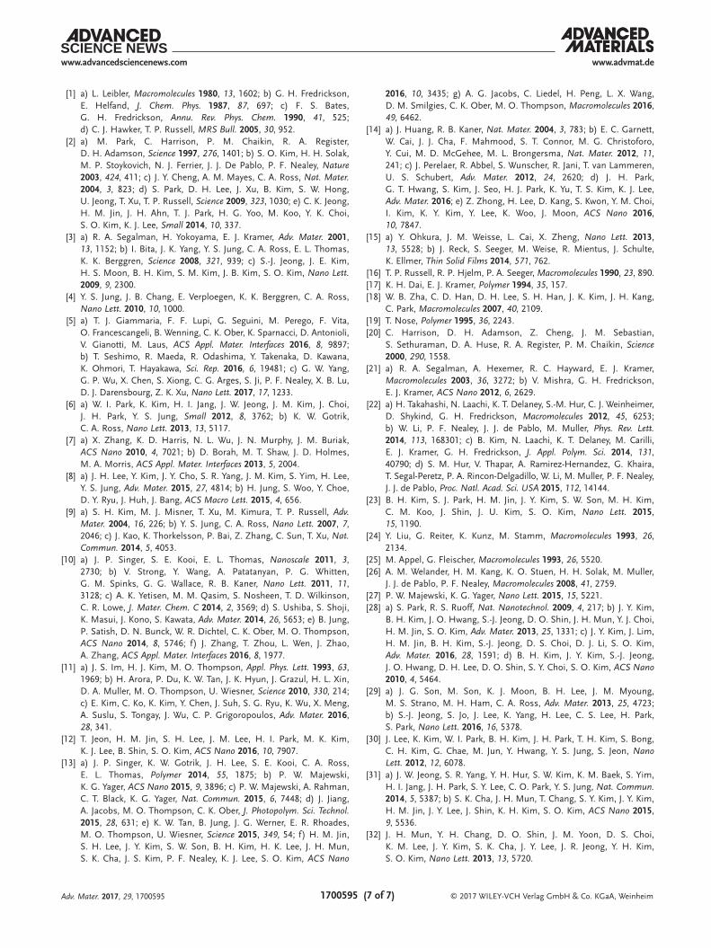
Motivated by the effective large grain growth, FLA was tested to confirm its compatibility with DSA process. Figure 4a–d shows the graphoepitaxial assembly[3] of BCPs by FLA. The self-assembled nanopattern of SD16 was successfully aligned along the 800 nm width topographical trench (Figure 4a). The sharp peaks in the fast Fourier transform (FFT) (Figure 4a, inset) illustrate the high degree of alignment of stripe pattern. By contrast, it was hard to produce a well-aligned stripe pattern of the same BCPs with conventional thermal annealing process (Figure 4b). SD16 formed well-aligned concentric pattern in circular trench (diameter: 800 nm) by FLA (Figure 4c). Addi-tionally, graphoepitaxial assembly of sphere forming SD24.8 was successfully demonstrated with FLA. Hexagonally ordered nanoscale spheres are well-ordered within the topographical trench.
A straightforward process compatibility with usual poly-meric flexible substrates is one of the major advantages of our FLA. Notably, FLA of BCPs on the flexible substrate is demonstrated by employing chemically modified graphene
(CMG)[28] as a flexible and conformal photothermal conversion layer (Figure S7, Supporting Information). Owing to the milli-second-scale photothermal process, the flexible polymeric sub-strate did not show any thermal damage under FLA. Figure 4e shows the self-assembled morphology of SD16 on CMG/poly-imide (PI) film. Effective photothermal conversion at CMG layer induces instantaneous heating within millisecond scale and subsequently, SD16 is well-assembled without any notice-able damage in the polymeric bottom substrate (Figure 4e, inset). A FLA process on a transparent nonplanar geometry is also demonstrated in Figure 4f. Taking advantage of the mechanical robustness and compliance, CMG light absorbing layer was successfully stabilized on a high curvature glass tube surface. After FLA, a well-ordered 8 nm scale self-assembled nanopattern was generated without any noticeable reflow of BCP layer.
In summary, a millisecond level rapid photothermal pro-cess with an extremely high temperature is successfully dem-onstrated to address the formidable challenge of intrinsic slow self-assembly kinetics for high-χ BCPs. A solvent-free, extremely high-temperature process in atmospheric condi-tions enabled by FLA is highly beneficial for a fab-compatible practical use of the self-assembly process. 2D large-area pro-cessability potentially integrated with a roll-to-roll continuous process may offer an unprecedented opportunity of sub-10 nm scale nanopatterning for next-generation nanodevices including electronics,[29] optoelectronics,[30] sensors,[31] catalysts,[32] and so on. Besides, this rapid photothermal process breakthroughs
Adv. Mater. 2017, 29, 1700595
Figure 3. Mechanism of rapid self-assembly by FLA. Different self-assembly mechanisms of a) low-χ and b) high-χ BCPs by FLA. Hypothetical energy surfaces for high-χ BCP self-assembly by c) conventional thermal annealing and d) FLA (i.e., suppressed χ from the high temperature).
© 2017 WILEY-VCH Verlag GmbH & Co. KGaA, Weinheim1700595 (6 of 7)
www.advmat.dewww.advancedsciencenews.com
Adv. Mater. 2017, 29, 1700595
the present process limitation, and will open up the enormous potential for novel design and functionalities of high-χ BCPs.
Supporting InformationSupporting Information is available from the Wiley Online Library or from the author.
AcknowledgementsH.M.J. and D.Y.P. contributed equally to this work. This work was supported by the National Creative Research Initiative (CRI) Center for Multi-Dimensional Directed Nanoscale Assembly (2015R1A3A2033061), the Grobal Frontier Hybrid Interface Materials (GFHIM) (2013M3A6B1078874), and the Nano-Material Technology Development Program (2016M3A7B4905613) through the National
Research Foundation of Korea (NRF) funded by the Ministry of Science, ICT and Future Planning. D.Y.P. and K.J.L. were supported by Creative Materials Discovery Program (NRF-2016M3D1A1900035).
Conflict of InterestThe authors declare no conflict of interest.
Keywordsblock copolymers, directed self-assembly, flash light, photothermal effects
Received: January 30, 2017Revised: May 1, 2017
Published online: June 21, 2017
Figure 4. Directed self-assembly (DSA) of SD16 on 800 nm width silicon trench by a) FLA (78.8 J cm−2, 1 time) and b) conventional thermal annealing (250 °C, 5 min). The insets of (a) and (b) show the FFT of each SEM image. c) A self-assembled concentric in-plane cylindrical pattern in a circular trench (diameter: 800 nm) by FLA (78.8 J cm−2, 1 time). d) DSA of a sphere forming SD24.8 in an 800 nm width topographical trench. The inset of (d) shows the FFT for the single grain of hexagonally packed sphere nanostructure. e) Self-assembled BCP pattern on a flexible CMG/polyimide (PI) substrate and f) on a nonplanar geometry. The insets of (e) and (f) show the photographic image of the CMG/PI substrate and the CMG/Glass pipet after FLA, respectively.
© 2017 WILEY-VCH Verlag GmbH & Co. KGaA, Weinheim1700595 (7 of 7)
www.advmat.dewww.advancedsciencenews.com
Adv. Mater. 2017, 29, 1700595
[1] a) L. Leibler, Macromolecules 1980, 13, 1602; b) G. H. Fredrickson, E. Helfand, J. Chem. Phys. 1987, 87, 697; c) F. S. Bates, G. H. Fredrickson, Annu. Rev. Phys. Chem. 1990, 41, 525; d) C. J. Hawker, T. P. Russell, MRS Bull. 2005, 30, 952.
[2] a) M. Park, C. Harrison, P. M. Chaikin, R. A. Register, D. H. Adamson, Science 1997, 276, 1401; b) S. O. Kim, H. H. Solak, M. P. Stoykovich, N. J. Ferrier, J. J. De Pablo, P. F. Nealey, Nature 2003, 424, 411; c) J. Y. Cheng, A. M. Mayes, C. A. Ross, Nat. Mater. 2004, 3, 823; d) S. Park, D. H. Lee, J. Xu, B. Kim, S. W. Hong, U. Jeong, T. Xu, T. P. Russell, Science 2009, 323, 1030; e) C. K. Jeong, H. M. Jin, J. H. Ahn, T. J. Park, H. G. Yoo, M. Koo, Y. K. Choi, S. O. Kim, K. J. Lee, Small 2014, 10, 337.
[3] a) R. A. Segalman, H. Yokoyama, E. J. Kramer, Adv. Mater. 2001, 13, 1152; b) I. Bita, J. K. Yang, Y. S. Jung, C. A. Ross, E. L. Thomas, K. K. Berggren, Science 2008, 321, 939; c) S.-J. Jeong, J. E. Kim, H. S. Moon, B. H. Kim, S. M. Kim, J. B. Kim, S. O. Kim, Nano Lett. 2009, 9, 2300.
[4] Y. S. Jung, J. B. Chang, E. Verploegen, K. K. Berggren, C. A. Ross, Nano Lett. 2010, 10, 1000.
[5] a) T. J. Giammaria, F. F. Lupi, G. Seguini, M. Perego, F. Vita, O. Francescangeli, B. Wenning, C. K. Ober, K. Sparnacci, D. Antonioli, V. Gianotti, M. Laus, ACS Appl. Mater. Interfaces 2016, 8, 9897; b) T. Seshimo, R. Maeda, R. Odashima, Y. Takenaka, D. Kawana, K. Ohmori, T. Hayakawa, Sci. Rep. 2016, 6, 19481; c) G. W. Yang, G. P. Wu, X. Chen, S. Xiong, C. G. Arges, S. Ji, P. F. Nealey, X. B. Lu, D. J. Darensbourg, Z. K. Xu, Nano Lett. 2017, 17, 1233.
[6] a) W. I. Park, K. Kim, H. I. Jang, J. W. Jeong, J. M. Kim, J. Choi, J. H. Park, Y. S. Jung, Small 2012, 8, 3762; b) K. W. Gotrik, C. A. Ross, Nano Lett. 2013, 13, 5117.
[7] a) X. Zhang, K. D. Harris, N. L. Wu, J. N. Murphy, J. M. Buriak, ACS Nano 2010, 4, 7021; b) D. Borah, M. T. Shaw, J. D. Holmes, M. A. Morris, ACS Appl. Mater. Interfaces 2013, 5, 2004.
[8] a) J. H. Lee, Y. Kim, J. Y. Cho, S. R. Yang, J. M. Kim, S. Yim, H. Lee, Y. S. Jung, Adv. Mater. 2015, 27, 4814; b) H. Jung, S. Woo, Y. Choe, D. Y. Ryu, J. Huh, J. Bang, ACS Macro Lett. 2015, 4, 656.
[9] a) S. H. Kim, M. J. Misner, T. Xu, M. Kimura, T. P. Russell, Adv. Mater. 2004, 16, 226; b) Y. S. Jung, C. A. Ross, Nano Lett. 2007, 7, 2046; c) J. Kao, K. Thorkelsson, P. Bai, Z. Zhang, C. Sun, T. Xu, Nat. Commun. 2014, 5, 4053.
[10] a) J. P. Singer, S. E. Kooi, E. L. Thomas, Nanoscale 2011, 3, 2730; b) V. Strong, Y. Wang, A. Patatanyan, P. G. Whitten, G. M. Spinks, G. G. Wallace, R. B. Kaner, Nano Lett. 2011, 11, 3128; c) A. K. Yetisen, M. M. Qasim, S. Nosheen, T. D. Wilkinson, C. R. Lowe, J. Mater. Chem. C 2014, 2, 3569; d) S. Ushiba, S. Shoji, K. Masui, J. Kono, S. Kawata, Adv. Mater. 2014, 26, 5653; e) B. Jung, P. Satish, D. N. Bunck, W. R. Dichtel, C. K. Ober, M. O. Thompson, ACS Nano 2014, 8, 5746; f) J. Zhang, T. Zhou, L. Wen, J. Zhao, A. Zhang, ACS Appl. Mater. Interfaces 2016, 8, 1977.
[11] a) J. S. Im, H. J. Kim, M. O. Thompson, Appl. Phys. Lett. 1993, 63, 1969; b) H. Arora, P. Du, K. W. Tan, J. K. Hyun, J. Grazul, H. L. Xin, D. A. Muller, M. O. Thompson, U. Wiesner, Science 2010, 330, 214; c) E. Kim, C. Ko, K. Kim, Y. Chen, J. Suh, S. G. Ryu, K. Wu, X. Meng, A. Suslu, S. Tongay, J. Wu, C. P. Grigoropoulos, Adv. Mater. 2016, 28, 341.
[12] T. Jeon, H. M. Jin, S. H. Lee, J. M. Lee, H. I. Park, M. K. Kim, K. J. Lee, B. Shin, S. O. Kim, ACS Nano 2016, 10, 7907.
[13] a) J. P. Singer, K. W. Gotrik, J. H. Lee, S. E. Kooi, C. A. Ross, E. L. Thomas, Polymer 2014, 55, 1875; b) P. W. Majewski, K. G. Yager, ACS Nano 2015, 9, 3896; c) P. W. Majewski, A. Rahman, C. T. Black, K. G. Yager, Nat. Commun. 2015, 6, 7448; d) J. Jiang, A. Jacobs, M. O. Thompson, C. K. Ober, J. Photopolym. Sci. Technol. 2015, 28, 631; e) K. W. Tan, B. Jung, J. G. Werner, E. R. Rhoades, M. O. Thompson, U. Wiesner, Science 2015, 349, 54; f) H. M. Jin, S. H. Lee, J. Y. Kim, S. W. Son, B. H. Kim, H. K. Lee, J. H. Mun, S. K. Cha, J. S. Kim, P. F. Nealey, K. J. Lee, S. O. Kim, ACS Nano
2016, 10, 3435; g) A. G. Jacobs, C. Liedel, H. Peng, L. X. Wang, D. M. Smilgies, C. K. Ober, M. O. Thompson, Macromolecules 2016, 49, 6462.
[14] a) J. Huang, R. B. Kaner, Nat. Mater. 2004, 3, 783; b) E. C. Garnett, W. Cai, J. J. Cha, F. Mahmood, S. T. Connor, M. G. Christoforo, Y. Cui, M. D. McGehee, M. L. Brongersma, Nat. Mater. 2012, 11, 241; c) J. Perelaer, R. Abbel, S. Wunscher, R. Jani, T. van Lammeren, U. S. Schubert, Adv. Mater. 2012, 24, 2620; d) J. H. Park, G. T. Hwang, S. Kim, J. Seo, H. J. Park, K. Yu, T. S. Kim, K. J. Lee, Adv. Mater. 2016; e) Z. Zhong, H. Lee, D. Kang, S. Kwon, Y. M. Choi, I. Kim, K. Y. Kim, Y. Lee, K. Woo, J. Moon, ACS Nano 2016, 10, 7847.
[15] a) Y. Ohkura, J. M. Weisse, L. Cai, X. Zheng, Nano Lett. 2013, 13, 5528; b) J. Reck, S. Seeger, M. Weise, R. Mientus, J. Schulte, K. Ellmer, Thin Solid Films 2014, 571, 762.
[16] T. P. Russell, R. P. Hjelm, P. A. Seeger, Macromolecules 1990, 23, 890.[17] K. H. Dai, E. J. Kramer, Polymer 1994, 35, 157.[18] W. B. Zha, C. D. Han, D. H. Lee, S. H. Han, J. K. Kim, J. H. Kang,
C. Park, Macromolecules 2007, 40, 2109.[19] T. Nose, Polymer 1995, 36, 2243.[20] C. Harrison, D. H. Adamson, Z. Cheng, J. M. Sebastian,
S. Sethuraman, D. A. Huse, R. A. Register, P. M. Chaikin, Science 2000, 290, 1558.
[21] a) R. A. Segalman, A. Hexemer, R. C. Hayward, E. J. Kramer, Macromolecules 2003, 36, 3272; b) V. Mishra, G. H. Fredrickson, E. J. Kramer, ACS Nano 2012, 6, 2629.
[22] a) H. Takahashi, N. Laachi, K. T. Delaney, S.-M. Hur, C. J. Weinheimer, D. Shykind, G. H. Fredrickson, Macromolecules 2012, 45, 6253; b) W. Li, P. F. Nealey, J. J. de Pablo, M. Muller, Phys. Rev. Lett. 2014, 113, 168301; c) B. Kim, N. Laachi, K. T. Delaney, M. Carilli, E. J. Kramer, G. H. Fredrickson, J. Appl. Polym. Sci. 2014, 131, 40790; d) S. M. Hur, V. Thapar, A. Ramirez-Hernandez, G. Khaira, T. Segal-Peretz, P. A. Rincon-Delgadillo, W. Li, M. Muller, P. F. Nealey, J. J. de Pablo, Proc. Natl. Acad. Sci. USA 2015, 112, 14144.
[23] B. H. Kim, S. J. Park, H. M. Jin, J. Y. Kim, S. W. Son, M. H. Kim, C. M. Koo, J. Shin, J. U. Kim, S. O. Kim, Nano Lett. 2015, 15, 1190.
[24] Y. Liu, G. Reiter, K. Kunz, M. Stamm, Macromolecules 1993, 26, 2134.
[25] M. Appel, G. Fleischer, Macromolecules 1993, 26, 5520.[26] A. M. Welander, H. M. Kang, K. O. Stuen, H. H. Solak, M. Muller,
J. J. de Pablo, P. F. Nealey, Macromolecules 2008, 41, 2759.[27] P. W. Majewski, K. G. Yager, Nano Lett. 2015, 15, 5221.[28] a) S. Park, R. S. Ruoff, Nat. Nanotechnol. 2009, 4, 217; b) J. Y. Kim,
B. H. Kim, J. O. Hwang, S.-J. Jeong, D. O. Shin, J. H. Mun, Y. J. Choi, H. M. Jin, S. O. Kim, Adv. Mater. 2013, 25, 1331; c) J. Y. Kim, J. Lim, H. M. Jin, B. H. Kim, S.-J. Jeong, D. S. Choi, D. J. Li, S. O. Kim, Adv. Mater. 2016, 28, 1591; d) B. H. Kim, J. Y. Kim, S.-J. Jeong, J. O. Hwang, D. H. Lee, D. O. Shin, S. Y. Choi, S. O. Kim, ACS Nano 2010, 4, 5464.
[29] a) J. G. Son, M. Son, K. J. Moon, B. H. Lee, J. M. Myoung, M. S. Strano, M. H. Ham, C. A. Ross, Adv. Mater. 2013, 25, 4723; b) S.-J. Jeong, S. Jo, J. Lee, K. Yang, H. Lee, C. S. Lee, H. Park, S. Park, Nano Lett. 2016, 16, 5378.
[30] J. Lee, K. Kim, W. I. Park, B. H. Kim, J. H. Park, T. H. Kim, S. Bong, C. H. Kim, G. Chae, M. Jun, Y. Hwang, Y. S. Jung, S. Jeon, Nano Lett. 2012, 12, 6078.
[31] a) J. W. Jeong, S. R. Yang, Y. H. Hur, S. W. Kim, K. M. Baek, S. Yim, H. I. Jang, J. H. Park, S. Y. Lee, C. O. Park, Y. S. Jung, Nat. Commun. 2014, 5, 5387; b) S. K. Cha, J. H. Mun, T. Chang, S. Y. Kim, J. Y. Kim, H. M. Jin, J. Y. Lee, J. Shin, K. H. Kim, S. O. Kim, ACS Nano 2015, 9, 5536.
[32] J. H. Mun, Y. H. Chang, D. O. Shin, J. M. Yoon, D. S. Choi, K. M. Lee, J. Y. Kim, S. K. Cha, J. Y. Lee, J. R. Jeong, Y. H. Kim, S. O. Kim, Nano Lett. 2013, 13, 5720.