FAN2500 100 mA CMOS LDO Regulator - Markit · mend exceeding them or designing to Absolute Maximum...
12
FAN2500 — 100 mA CMOS LDO Regulator © 2010 Fairchild Semiconductor Corporation www.fairchildsemi.com FAN2500 Rev. 1.1.0 1 May 2013 FAN2500 100 mA CMOS LDO Regulator Features • Ultra-Low Power Consumption • 100 mV Dropout Voltage at 100 mA • 25 μA Ground Current at 100 mA • Enable / Shutdown Control • SOT23-5 package • Thermal Limiting • 300 mA Peak Current Applications • Mobile Phones and Accessories • Portable Cameras and Video Recorders • Laptop, Notebook, and Palmtop Computers Ordering Information Tape and Reel Information Part Number V OUT Pin 4 Function Top Mark Package Packing Method FAN2500S25X 2.5 Bypass ACE SOT-23 5L Tape and Reel FAN2500S30X 3.0 Bypass ACW SOT-23 5L Tape and Reel FAN2500S33X 3.3 Bypass AC3 SOT-23 5L Tape and Reel FAN2500SX Adj. Adjust ACA SOT-23 5L Tape and Reel Quantity Reel Size Width 3000 7 inches 8 mm Description The FAN2500 micropower low-dropout voltage regulator utilizes CMOS technology to offer a new level of cost- effective performance in mobile handsets, laptop and notebook portable computers, and other portable devices. Features include extremely low power consump- tion, low shutdown current, low dropout voltage, excep- tional loop stability able to accommodate a wide variety of external capacitors, and a compact SOT23-5 surface- mount package. The FAN2500 offers significant improve- ments over older BiCMOS designs and is pin-compatible with many popular devices. The output is thermally pro- tected against overload. FAN2500: pin 4 – ADJ, allows the user to adjust the output voltage over a wide range using an external volt- age divider. FAN2500-XX: pin 4 – BYP, to which a bypass capacitor may be connected for optimal noise performance. Output voltage is fixed, indicated by the suffix XX. The standard fixed output voltages available are 2.5 V, 3.0 V, and 3.3 V.
Transcript of FAN2500 100 mA CMOS LDO Regulator - Markit · mend exceeding them or designing to Absolute Maximum...
FA
N2500 —
100 mA
CM
OS
LD
O R
egu
lator
© 2010 Fairchild Semiconductor Corporation www.fairchildsemi.com
FAN2500 Rev. 1.1.0 1
May 2013
FAN2500100 mA CMOS LDO Regulator
Features• Ultra-Low Power Consumption• 100 mV Dropout Voltage at 100 mA• 25 μA Ground Current at 100 mA• Enable / Shutdown Control• SOT23-5 package• Thermal Limiting• 300 mA Peak Current
Applications• Mobile Phones and Accessories• Portable Cameras and Video Recorders• Laptop, Notebook, and Palmtop Computers
Ordering Information
Tape and Reel Information
Part Number VOUT Pin 4 Function Top Mark PackagePacking Method
FAN2500S25X 2.5 Bypass ACE SOT-23 5L Tape and Reel
FAN2500S30X 3.0 Bypass ACW SOT-23 5L Tape and Reel
FAN2500S33X 3.3 Bypass AC3 SOT-23 5L Tape and Reel
FAN2500SX Adj. Adjust ACA SOT-23 5L Tape and Reel
Quantity Reel Size Width
3000 7 inches 8 mm
DescriptionThe FAN2500 micropower low-dropout voltage regulatorutilizes CMOS technology to offer a new level of cost-effective performance in mobile handsets, laptop andnotebook portable computers, and other portabledevices. Features include extremely low power consump-tion, low shutdown current, low dropout voltage, excep-tional loop stability able to accommodate a wide variety ofexternal capacitors, and a compact SOT23-5 surface-mount package. The FAN2500 offers significant improve-ments over older BiCMOS designs and is pin-compatiblewith many popular devices. The output is thermally pro-tected against overload.
FAN2500: pin 4 – ADJ, allows the user to adjust the
output voltage over a wide range using an external volt-age divider.
FAN2500-XX: pin 4 – BYP, to which a bypass capacitor
may be connected for optimal noise performance. Output
voltage is fixed, indicated by the suffix XX.
The standard fixed output voltages available are 2.5 V,
3.0 V, and 3.3 V.
FA
N2500 —
100 mA
CM
OS
LD
O R
egu
lator
© 2010 Fairchild Semiconductor Corporation www.fairchildsemi.com
FAN2500 Rev. 1.1.0 2
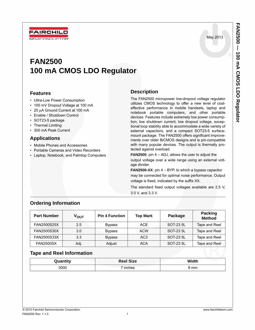
Block Diagram
Figure 1. Block Diagram
Pin Configuration
Figure 2. Pin Configuration
Pin Descriptions
Pin No. FAN2500 FAN2500-XX
1. VIN VIN
2. GND GND
3. EN EN
4. ADJ BYP
5. VOUT VOUT
Pin Name Pin No. Type Functional Description
ADJ 4 InputFAN2500 AdjustRatio of potential divider from VOUT to ADJ determines output voltage
BYP 4 PassiveFAN2500-XX BypassConnect a 470 pF capacitor for noise reduction
EN 3 Digital Input
Enable0: Shutdown VOUT
1: Enable VOUT
VIN 1 Power InVoltage InputSupply voltage input
VOUT 5 Power OutVoltage OutputRegulated output voltage
GND 2 Power Ground
FAN2500
FA
N2500 —
100 mA
CM
OS
LD
O R
egu
lator
© 2010 Fairchild Semiconductor Corporation www.fairchildsemi.com
FAN2500 Rev. 1.1.0 3
Absolute Maximum Ratings(1)
Stresses exceeding the absolute maximum ratings may damage the device. The device may not function or be opera-ble above the recommended operating conditions and stressing the parts to these levels is not recommended. In addi-tion, extended exposure to stresses above the recommended operating conditions may affect device reliability. The absolute maximum ratings are stress ratings only.
Notes:
1. Functional operation under any of these conditions is NOT implied. Performance and reliability are guaranteed only
if Recommended Operating Conditions are not exceeded.
2. Applied voltage must be current limited to specified range.
3. Based upon thermally limited junction temperature:
4. Human Body Model is 4 kV minimum using Mil Std. 883E, method 3015.7. Machine Model is 400 V minimum using
JEDEC method A115-A.
Recommended Operating Conditions
The recommended Operating Conditions table defines the conditions for actual device operation. Recommended oper-ating conditions are specified to ensure optimal performance to the datasheet specifications. Fairchild does not recom-mend exceeding them or designing to Absolute Maximum Ratings.
Parameter Min. Max. Unit
Power Supply Voltages
VIN (Measured to GND) 0 7 V
Enable Input (EN)
Applied Voltage (Measured to GND)(2) 0 7 V
Power
Dissipation(3) Internally Limited
Temperature
Junction -65 150 °C
Lead Soldering (5 s) 260 °C
Storage -65 150 °C
Electrostatic Discharge(4) 4 kV
Symbol Parameter Min. Nom. Max. UnitVIN Input Voltage Range 2.7 6.5 V
VEN Enable Input Voltage 0 VIN V
TJ Junction Temperature -40 +125 °C
θJA Thermal Resistance, Junction to Air 220 °C/W
θJC Thermal Resistance, Junction to Case 130 °C/W
PDTJ max( ) TA–
ΘJA-------------------------------=
FA
N2500 —
100 mA
CM
OS
LD
O R
egu
lator
© 2010 Fairchild Semiconductor Corporation www.fairchildsemi.com
FAN2500 Rev. 1.1.0 4
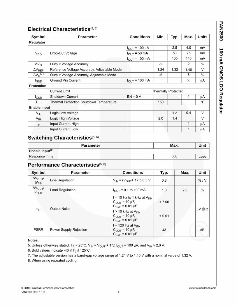
Electrical Characteristics(5, 6)
Switching Characteristics(5, 6)
Performance Characteristics(5, 6)
Notes:
5. Unless otherwise stated; TA = 25°C, VIN = VOUT + 1 V, IOUT = 100 μA, and VIH > 2.0 V.
6. Bold values indicate -40 ≤ TJ ≤ 125°C.
7. The adjustable version has a band-gap voltage range of 1.24 V to 1.40 V with a nominal value of 1.32 V.
8. When using repeated cycling.
Symbol Parameter Conditions Min. Typ. Max. UnitsRegulator
VDO Drop-Out Voltage
IOUT = 100 μA 2.5 4.0 mV
IOUT = 50 mA 50 75 mV
IOUT = 100 mA 100 140 mV
∆VO Output Voltage Accuracy -2 2 %
∆VREF Reference Voltage Accuracy, Adjustable Mode 1.24 1.32 1.40 V
∆VO(7) Output Voltage Accuracy, Adjustable Mode -6 6 %
IGND Ground Pin Current IOUT = 100 mA 50 μA
Protection
Current Limit Thermally Protected
IGSD Shutdown Current EN = 0 V 1 μA
TSH Thermal Protection Shutdown Temperature 150 °C
Enable Input
VIL Logic Low Voltage 1.2 0.4 V
VIH Logic High Voltage 2.0 1.4 V
IIH Input Current High 1 μA
II Input Current Low 1 μA
Parameter Max. UnitEnable Input(8)
Response Time 500 μsec
Symbol Parameter Conditions Typ. Max. Unit∆VOUT/∆VIN
Line Regulation VIN = (VOUT+ 1) to 6.5 V 0.3 % / V
∆VOUT/VOUT
Load Regulation IOUT = 0.1 to 100 mA 1.0 2.0 %
eN Output Noise
f = 10 Hz to 1 kHz at VIN,COUT = 10 μF,CBYP = 0.01 μF
< 7.00
μV / Hzf > 10 kHz at VIN,COUT = 10 μF,CBYP = 0.01 μF
< 0.01
PSRR Power Supply Rejectionf = 120 Hz at VIN,COUT = 10 μF,CBYP = 0.01 μF
43 dB
FA
N2500 —
100 mA
CM
OS
LD
O R
egu
lator
© 2010 Fairchild Semiconductor Corporation www.fairchildsemi.com
FAN2500 Rev. 1.1.0 5
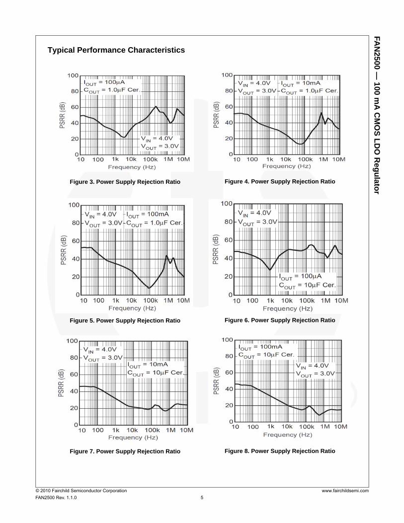
Typical Performance Characteristics
Figure 3. Power Supply Rejection Ratio Figure 4. Power Supply Rejection Ratio
Figure 5. Power Supply Rejection Ratio Figure 6. Power Supply Rejection Ratio
Figure 7. Power Supply Rejection Ratio Figure 8. Power Supply Rejection Ratio
FA
N2500 —
100 mA
CM
OS
LD
O R
egu
lator
© 2010 Fairchild Semiconductor Corporation www.fairchildsemi.com
FAN2500 Rev. 1.1.0 6
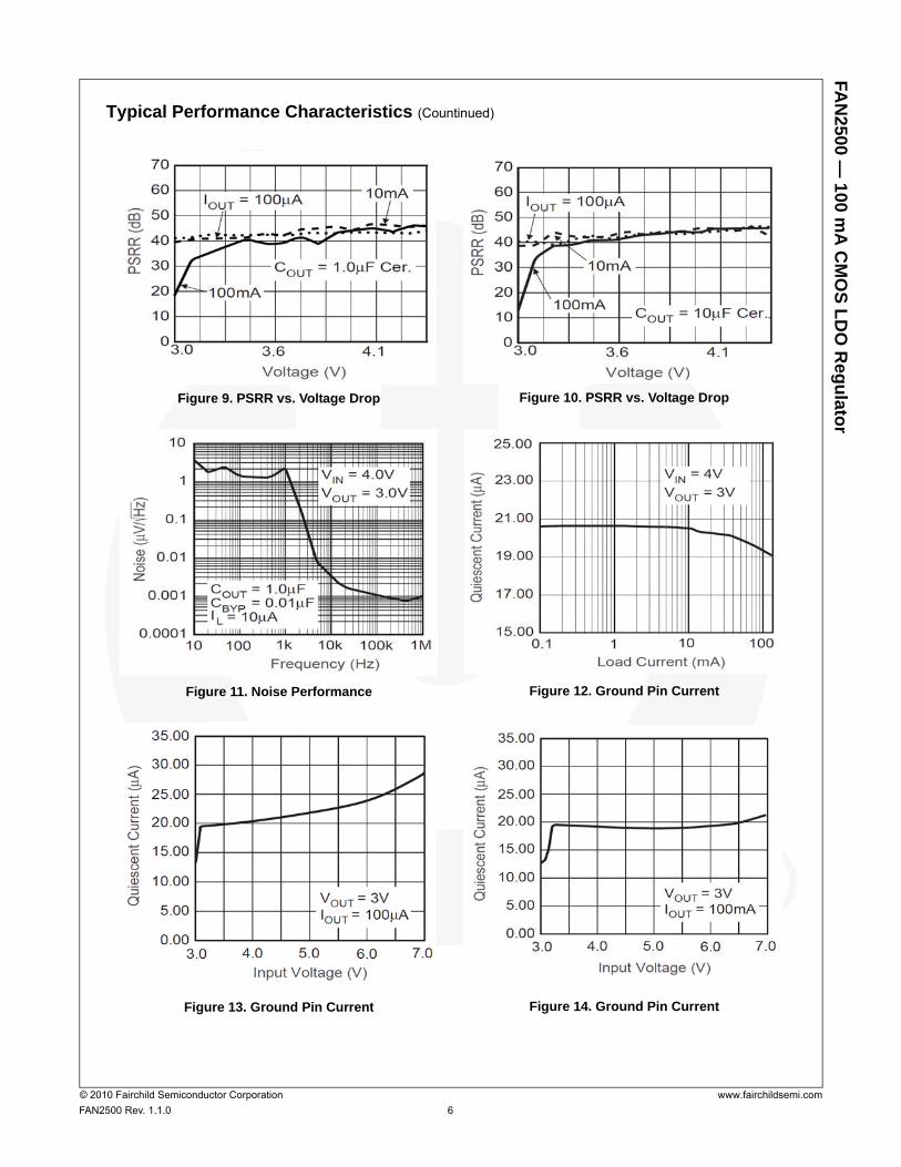
Typical Performance Characteristics (Countinued)
Figure 9. PSRR vs. Voltage Drop Figure 10. PSRR vs. Voltage Drop
Figure 11. Noise Performance Figure 12. Ground Pin Current
Figure 13. Ground Pin Current Figure 14. Ground Pin Current
FA
N2500 —
100 mA
CM
OS
LD
O R
egu
lator
© 2010 Fairchild Semiconductor Corporation www.fairchildsemi.com
FAN2500 Rev. 1.1.0 7
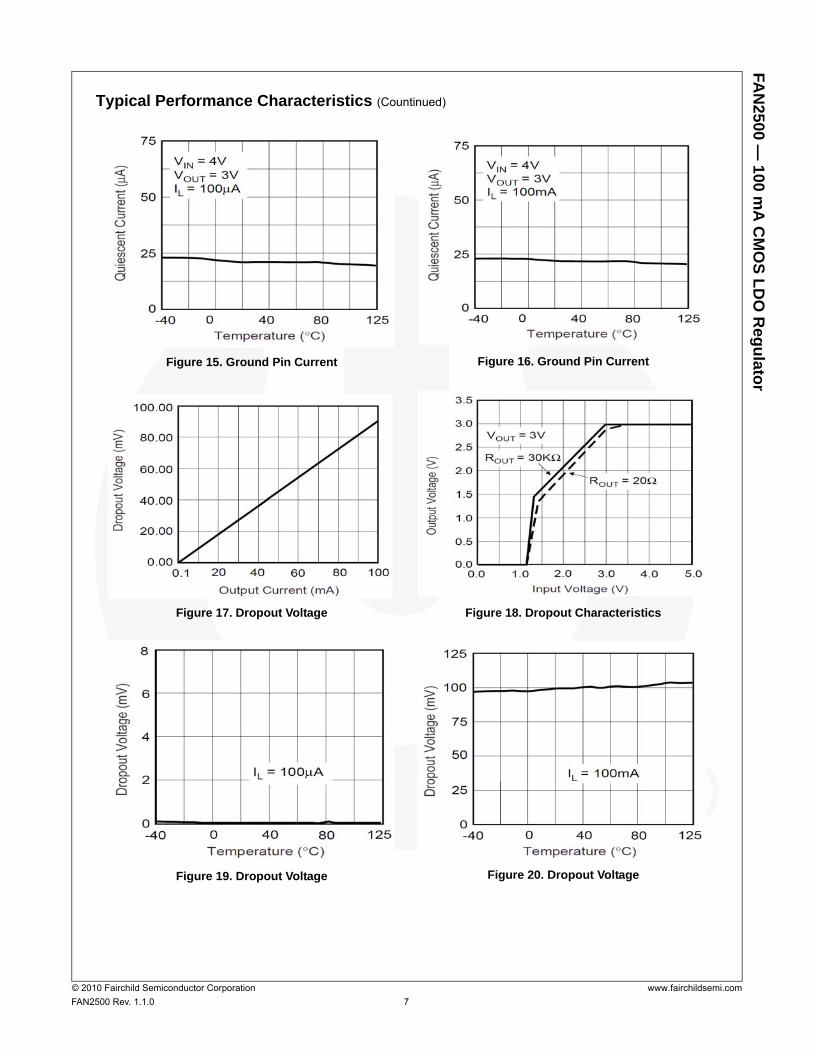
Typical Performance Characteristics (Countinued)
Figure 15. Ground Pin Current Figure 16. Ground Pin Current
Figure 17. Dropout Voltage Figure 18. Dropout Characteristics
Figure 19. Dropout Voltage Figure 20. Dropout Voltage
FA
N2500 —
100 mA
CM
OS
LD
O R
egu
lator
© 2010 Fairchild Semiconductor Corporation www.fairchildsemi.com
FAN2500 Rev. 1.1.0 8
Typical Performance Characteristics (Countinued)
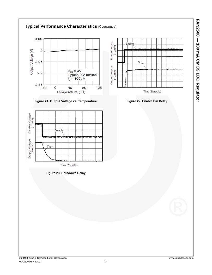
Figure 21. Output Voltage vs. Temperature Figure 22. Enable Pin Delay
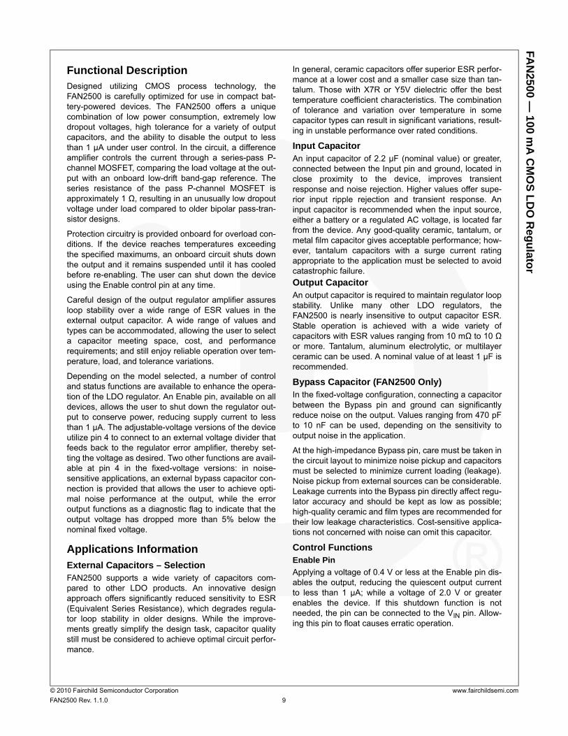
Figure 23. Shutdown Delay
FA
N2500 —
100 mA
CM
OS
LD
O R
egu
lator
© 2010 Fairchild Semiconductor Corporation www.fairchildsemi.com
FAN2500 Rev. 1.1.0 9
Functional DescriptionDesigned utilizing CMOS process technology, theFAN2500 is carefully optimized for use in compact bat-tery-powered devices. The FAN2500 offers a uniquecombination of low power consumption, extremely lowdropout voltages, high tolerance for a variety of outputcapacitors, and the ability to disable the output to lessthan 1 μA under user control. In the circuit, a differenceamplifier controls the current through a series-pass P-channel MOSFET, comparing the load voltage at the out-put with an onboard low-drift band-gap reference. Theseries resistance of the pass P-channel MOSFET isapproximately 1 Ω, resulting in an unusually low dropoutvoltage under load compared to older bipolar pass-tran-sistor designs.
Protection circuitry is provided onboard for overload con-ditions. If the device reaches temperatures exceedingthe specified maximums, an onboard circuit shuts downthe output and it remains suspended until it has cooledbefore re-enabling. The user can shut down the deviceusing the Enable control pin at any time.
Careful design of the output regulator amplifier assuresloop stability over a wide range of ESR values in theexternal output capacitor. A wide range of values andtypes can be accommodated, allowing the user to selecta capacitor meeting space, cost, and performancerequirements; and still enjoy reliable operation over tem-perature, load, and tolerance variations.
Depending on the model selected, a number of controland status functions are available to enhance the opera-tion of the LDO regulator. An Enable pin, available on alldevices, allows the user to shut down the regulator out-put to conserve power, reducing supply current to lessthan 1 μA. The adjustable-voltage versions of the deviceutilize pin 4 to connect to an external voltage divider thatfeeds back to the regulator error amplifier, thereby set-ting the voltage as desired. Two other functions are avail-able at pin 4 in the fixed-voltage versions: in noise-sensitive applications, an external bypass capacitor con-nection is provided that allows the user to achieve opti-mal noise performance at the output, while the erroroutput functions as a diagnostic flag to indicate that theoutput voltage has dropped more than 5% below thenominal fixed voltage.
Applications InformationExternal Capacitors – SelectionFAN2500 supports a wide variety of capacitors com-pared to other LDO products. An innovative designapproach offers significantly reduced sensitivity to ESR(Equivalent Series Resistance), which degrades regula-tor loop stability in older designs. While the improve-ments greatly simplify the design task, capacitor qualitystill must be considered to achieve optimal circuit perfor-mance.
In general, ceramic capacitors offer superior ESR perfor-mance at a lower cost and a smaller case size than tan-talum. Those with X7R or Y5V dielectric offer the besttemperature coefficient characteristics. The combinationof tolerance and variation over temperature in somecapacitor types can result in significant variations, result-ing in unstable performance over rated conditions.
Input CapacitorAn input capacitor of 2.2 μF (nominal value) or greater,connected between the Input pin and ground, located inclose proximity to the device, improves transientresponse and noise rejection. Higher values offer supe-rior input ripple rejection and transient response. Aninput capacitor is recommended when the input source,either a battery or a regulated AC voltage, is located farfrom the device. Any good-quality ceramic, tantalum, ormetal film capacitor gives acceptable performance; how-ever, tantalum capacitors with a surge current ratingappropriate to the application must be selected to avoidcatastrophic failure.
Output CapacitorAn output capacitor is required to maintain regulator loopstability. Unlike many other LDO regulators, theFAN2500 is nearly insensitive to output capacitor ESR.Stable operation is achieved with a wide variety ofcapacitors with ESR values ranging from 10 mΩ to 10 Ωor more. Tantalum, aluminum electrolytic, or multilayerceramic can be used. A nominal value of at least 1 μF isrecommended.
Bypass Capacitor (FAN2500 Only)In the fixed-voltage configuration, connecting a capacitorbetween the Bypass pin and ground can significantlyreduce noise on the output. Values ranging from 470 pFto 10 nF can be used, depending on the sensitivity tooutput noise in the application.
At the high-impedance Bypass pin, care must be taken inthe circuit layout to minimize noise pickup and capacitorsmust be selected to minimize current loading (leakage).Noise pickup from external sources can be considerable.Leakage currents into the Bypass pin directly affect regu-lator accuracy and should be kept as low as possible;high-quality ceramic and film types are recommended fortheir low leakage characteristics. Cost-sensitive applica-tions not concerned with noise can omit this capacitor.
Control FunctionsEnable Pin
Applying a voltage of 0.4 V or less at the Enable pin dis-ables the output, reducing the quiescent output currentto less than 1 μA; while a voltage of 2.0 V or greaterenables the device. If this shutdown function is notneeded, the pin can be connected to the VIN pin. Allow-ing this pin to float causes erratic operation.
FA
N2500 —
100 mA
CM
OS
LD
O R
egu
lator
© 2010 Fairchild Semiconductor Corporation www.fairchildsemi.com
FAN2500 Rev. 1.1.0 10
Thermal ProtectionFAN2500 can supply high peak output currents of up to 1A for brief periods. However, this output load causes thedevice temperature to exceed maximum ratings due topower dissipation. During output overload conditions,when the die temperature exceeds the shutdown limittemperature of 150°C, onboard thermal protection dis-ables the output until the temperature drops below thislimit, at which point the output is re-enabled. During athermal shutdown situation, the user may assert thepower-down function at the Enable pin, reducing powerconsumption to the minimum level IGND· VIN.
Thermal Characteristics
FAN2500 can supply 100 mA at the specified output volt-age with an operating die (junction) temperature of up to125°C. Once the power dissipation and thermal resis-tance is known, the maximum junction temperature ofthe device can be calculated. While the power dissipa-tion is calculated from known electrical parameters, thethermal resistance is a result of the thermal characteris-tics of the compact SOT23-5 surface-mount packageand the surrounding PC board copper to which it ismounted.
The power dissipation is equal to the product of the inputto output voltage differential and the output current, plusthe ground current multiplied by the input voltage, or:
The ground pin current, IGND, can be found in the chartsprovided in the Electrical Characteristics section.
The relationship describing the thermal behavior of thepackage is:
where TJ(max) is the maximum allowable junction temper-ature of the die, which is 125°C, and TA is the ambientoperating temperature. θJA is dependent on the sur-rounding PC board layout and can be empiricallyobtained. While the θJC (junction-to-case) of the SOT23-5 package is specified at 130°C /W, the θJA of the mini-mum PWB footprint is at least 235°C/W. This can beimproved by providing a heat sink of surrounding copperground on the PCB.
Depending on the size of the copper area, the resultingθJA can range from approximately 180°C/W for onesquare inch to nearly 130°C/W for four square inches.The addition of backside copper with through-holes, stiff-eners, and other enhancements can reduce this value.The heat contributed by the dissipation of other devicesnearby must be included in design considerations.
PD VIN VOUT–( )IOUT VINIGND+=
PD max( )TJ max( ) TA–
θJA-------------------------------
⎩ ⎭⎨ ⎬⎧ ⎫
=
Once the limiting parameters in these two relationshipshave been determined, the design can be modified toensure that the device remains within specified operatingconditions at all times.
If overload conditions are not considered, it is possiblefor the device to enter a thermal cycling loop, in whichthe circuit enters a shutdown condition, cools, re-enables, and then again overheats and shuts downrepeatedly due to an unmanaged fault condition.
Operational of Adjustable VersionThe adjustable version of the FAN2500 includes an inputpin, ADJ, which allows the user to select an output volt-age ranging from 1.8 V to near VIN, using an externalresistor divider. The voltage VADJ presented to the ADJpin is fed to the onboard error amplifier, which adjuststhe output voltage until VADJ is equal to the onboardbandgap reference voltage of 1.32 V (typ). The equationis:
The total value of the resistor chain should not exceed
250 kΩ total to keep the error amplifier biased during no-load conditions. Programming output voltages very near
VIN need to allow for the magnitude and variation of the
dropout voltage VDO over load, supply, and temperature
variations. Note that the low-leakage MOSFET input tothe CMOS error amplifier induces no bias current error tothe calculation.
General PCB Layout Considerations
To achieve the full performance of the device, careful cir-cuit layout and grounding technique must be observed.Establishing a small local ground, to which the GND pin,the output, and bypass capacitors are connected; is rec-ommended. The input capacitor should be grounded tothe main ground plane. The quiet local ground is routedback to the main ground plane using feed-through vias.In general, the high-frequency compensation compo-nents (input, bypass, and output capacitors) should belocated as close to the device as possible. The proxim-ity of the output capacitor is especially important toachieve optimal noise compensation from the onboarderror amplifier, especially during high load conditions. Alarge copper area in the local ground provides the heatsinking discussed above when high power dissipationsignificantly increases the temperature of the device.
Component-side copper provides significantly betterthermal performance for this surface-mount device, com-pared to that obtained when using only copper planes onthe underside.
FA
N2500 —
100 mA
CM
OS
LD
O R
egu
lator
© 2010 Fairchild Semiconductor Corporation www.fairchildsemi.com
FAN2500 Rev. 1.1.0 11
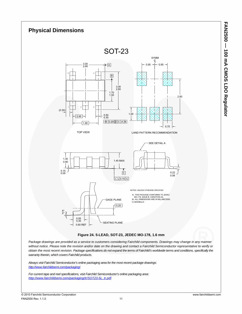
Physical Dimensions
Figure 24. 5-LEAD, SOT-23, JEDEC MO-178, 1.6 mm
Package drawings are provided as a service to customers considering Fairchild components. Drawings may change in any manner without notice. Please note the revision and/or date on the drawing and contact a Fairchild Semiconductor representative to verify or obtain the most recent revision. Package specifications do not expand the terms of Fairchild’s worldwide terms and conditions, specifically the warranty therein, which covers Fairchild products.
Always visit Fairchild Semiconductor’s online packaging area for the most recent package drawings:http://www.fairchildsemi.com/packaging/.
For current tape and reel specifications, visit Fairchild Semiconductor’s online packaging area:http://www.fairchildsemi.com/packaging/tr/SOT23-5L_tr.pdf.
5
1
4
32
LAND PATTERN RECOMMENDATION
B
A
L
C
0.10 C
0.20 C A B
0.60 REF
0.550.35
SEATING PLANE
0.25
GAGE PLANE
8°0°
NOTES: UNLESS OTHEWISE SPECIFIED
A) THIS PACKAGE CONFORMS TO JEDEC
MO-178, ISSUE B, VARIATION AA,
B) ALL DIMENSIONS ARE IN MILLIMETERS.
1.45 MAX1.30
0.90
0.150.05
1.90
0.950.500.30
3.002.60
1.701.50
3.002.80
SYMMC
0.950.95
2.60
0.70
1.00
SEE DETAIL A
0.22
0.08
C) MA05Brev5
TOP VIEW
(0.30)
SOT-23
© Fairchild Semiconductor Corporation www.fairchildsemi.com
TRADEMARKS
The following includes registered and unregistered trademarks and service marks, owned by Fairchild Semiconductor and/or its global subsidiaries, and is not intended to be an exhaustive list of all such trademarks.
2Cool
AccuPowerAX-CAP
®*
BitSiC
Build it Now
CorePLUS
CorePOWER
CROSSVOLTCTL
Current Transfer LogicDEUXPEED
®
Dual Cool™ EcoSPARK
®
EfficientMax
ESBC
Fairchild®
Fairchild Semiconductor®
FACT Quiet SeriesFACT
®
FAST®
FastvCore
FETBench
FPS
F-PFSFRFET
®
Global Power ResourceSM
GreenBridge
Green FPS
Green FPS e-Series
GmaxGTO
IntelliMAX
ISOPLANARMaking Small Speakers Sound Louder
and Better™
MegaBuck
MICROCOUPLER
MicroFET
MicroPak
MicroPak2
MillerDrive
MotionMax
mWSaver
OptoHiTOPTOLOGIC
®
OPTOPLANAR®
®
PowerTrench®
PowerXS™
Programmable Active DroopQFET
®
QS
Quiet Series
RapidConfigure
Saving our world, 1mW/W/kW at a time™
SignalWise
SmartMax
SMART START
Solutions for Your SuccessSPM
®
STEALTHSuperFET
®
SuperSOT -3
SuperSOT -6
SuperSOT -8 SupreMOS
®
SyncFET
Sync-Lock™
®*
TinyBoost
TinyBuck
TinyCalcTinyLogic
®
TINYOPTO
TinyPower
TinyPWM
TinyWire
TranSiC
TriFault DetectTRUECURRENT
®*
SerDes
UHC®
Ultra FRFET
UniFET
VCX
VisualMax
VoltagePlusXS™
* Trademarks of System General Corporation, used under license by Fairchild Semiconductor.
DISCLAIMER FAIRCHILD SEMICONDUCTOR RESERVES THE RIGHT TO MAKE CHANGES WITHOUT FURTHER NOTICE TO ANY PRODUCTS HEREIN TO IMPROVE RELIABILITY, FUNCTION, OR DESIGN. FAIRCHILD DOES NOT ASSUME ANY LIABILITY ARISING OUT OF THE APPLICATION OR USE OF ANY PRODUCT OR CIRCUIT DESCRIBED HEREIN; NEITHER DOES IT CONVEY ANY LICENSE UNDER ITS PATENT RIGHTS, NOR THE RIGHTS OF OTHERS. THESE SPECIFICATIONS DO NOT EXPAND THE TERMS OF FAIRCHILD’S WORLDWIDE TERMS AND CONDITIONS, SPECIFICALLY THE WARRANTY THEREIN, WHICH COVERS THESE PRODUCTS.
LIFE SUPPORT POLICY FAIRCHILD’S PRODUCTS ARE NOT AUTHORIZED FOR USE AS CRITICAL COMPONENTS IN LIFE SUPPORT DEVICES OR SYSTEMS WITHOUT THE EXPRESS WRITTEN APPROVAL OF FAIRCHILD SEMICONDUCTOR CORPORATION.
As used herein:
1. Life support devices or systems are devices or systems which, (a) are intended for surgical implant into the body or (b) support or sustain life, and (c) whose failure to perform when properly used in accordance with instructions for use provided in the labeling, can be reasonably expected to result in a significant injury of the user.
2. A critical component in any component of a life support, device, or system whose failure to perform can be reasonably expected to cause the failure of the life support device or system, or to affect its safety or effectiveness.
ANTI-COUNTERFEITING POLICY Fairchild Semiconductor Corporation's Anti-Counterfeiting Policy. Fairchild's Anti-Counterfeiting Policy is also stated on our external website, www.fairchildsemi.com, under Sales Support.
Counterfeiting of semiconductor parts is a growing problem in the industry. All manufacturers of semiconductor products are experiencing counterfeiting of their parts. Customers who inadvertently purchase counterfeit parts experience many problems such as loss of brand reputation, substandard performance, failed applications, and increased cost of production and manufacturing delays. Fairchild is taking strong measures to protect ourselves and our customers from the proliferation of counterfeit parts. Fairchild strongly encourages customers to purchase Fairchild parts either directly from Fairchild or from Authorized Fairchild Distributors who are listed by country on our web page cited above. Products customers buy either from Fairchild directly or from Authorized Fairchild Distributors are genuine parts, have full traceability, meet Fairchild's quality standards for handling and storage and provide access to Fairchild's full range of up-to-date technical and product information. Fairchild and our Authorized Distributors will stand behind all warranties and will appropriately address any warranty issues that may arise. Fairchild will not provide any warranty coverage or other assistance for parts bought from Unauthorized Sources. Fairchild is committed to combat this global problem and encourage our customers to do their part in stopping this practice by buying direct or from authorized distributors.
PRODUCT STATUS DEFINITIONS
Definition of Terms Datasheet Identification Product Status Definition
Advance Information Formative / In Design Datasheet contains the design specifications for product development. Specifications may change in any manner without notice.
Preliminary First Production Datasheet contains preliminary data; supplementary data will be published at a later date. Fairchild Semiconductor reserves the right to make changes at any time without notice to improve design.
No Identification Needed Full Production Datasheet contains final specifications. Fairchild Semiconductor reserves the right to make changes at any time without notice to improve the design.
Obsolete Not In Production Datasheet contains specifications on a product that is discontinued by Fairchild Semiconductor. The datasheet is for reference information only.
Rev. I64
®


![GWS 21-180/230 (J)HV GWS 24-180/230 (J)BV · * The values given are valid for nominal voltages [U] of 230/240 V. For lower voltages and models for specific countries, For lower voltages](https://static.fdocument.org/doc/165x107/5c60d84909d3f2256a8c2c57/gws-21-180230-jhv-gws-24-180230-jbv-the-values-given-are-valid-for-nominal.jpg)