Experimental evidences of topological surface states …yuting/Publications/Publication 2013... ·...
13
Experimental evidences of topological surface states of β-Ag2Te Azat Sulaev, Peng Ren, Bin Xia, Qing Hua Lin, Ting Yu et al. Citation: AIP Advances 3, 032123 (2013); doi: 10.1063/1.4795735 View online: http://dx.doi.org/10.1063/1.4795735 View Table of Contents: http://aipadvances.aip.org/resource/1/AAIDBI/v3/i3 Published by the AIP Publishing LLC. Additional information on AIP Advances Journal Homepage: http://aipadvances.aip.org Journal Information: http://aipadvances.aip.org/about/journal Top downloads: http://aipadvances.aip.org/most_downloaded Information for Authors: http://aipadvances.aip.org/authors Downloaded 03 Aug 2013 to 155.69.4.4. All article content, except where otherwise noted, is licensed under a Creative Commons Attribution 3.0 Unported license. See: http://creativecommons.org/licenses/by/3.0/
Transcript of Experimental evidences of topological surface states …yuting/Publications/Publication 2013... ·...
Experimental evidences of topological surface states of β-Ag2TeAzat Sulaev, Peng Ren, Bin Xia, Qing Hua Lin, Ting Yu et al. Citation: AIP Advances 3, 032123 (2013); doi: 10.1063/1.4795735 View online: http://dx.doi.org/10.1063/1.4795735 View Table of Contents: http://aipadvances.aip.org/resource/1/AAIDBI/v3/i3 Published by the AIP Publishing LLC. Additional information on AIP AdvancesJournal Homepage: http://aipadvances.aip.org Journal Information: http://aipadvances.aip.org/about/journal Top downloads: http://aipadvances.aip.org/most_downloaded Information for Authors: http://aipadvances.aip.org/authors
Downloaded 03 Aug 2013 to 155.69.4.4. All article content, except where otherwise noted, is licensed under a Creative Commons Attribution 3.0 Unported license.See: http://creativecommons.org/licenses/by/3.0/
AIP ADVANCES 3, 032123 (2013)
Experimental evidences of topological surfacestates of β-Ag2Te
Azat Sulaev,1,a Peng Ren,1,a Bin Xia,1 Qing Hua Lin,1 Ting Yu,1 Caiyu Qiu,1
Shuang-Yuan Zhang,2 Ming-Yong Han,2 Zhi Peng Li,3 Wei Guang Zhu,3
Qingyu Wu,4 Yuan Ping Feng,4 Lei Shen,4,b Shun-Qing Shen,5
and Lan Wang1,b
1School of Physical and Mathematical Science, Nanyang Technological University,Singapore, 637371, Singapore2Institute of Materials Research and Engineering, Singapore, 117602, Singapore3School of Electrical and Electronic Engineering, Nanyang Technological University,Singapore, 639789, Singapore4Department of Physics, National University of Singapore, Singapore5Department of Physics, The University of Hong Kong, Pokfulam Road, Hong Kong,People’s Republic of China
(Received 20 December 2012; accepted 27 February 2013; published online 12 March 2013)
We present evidence of topological surface states in β-Ag2Te through first-principlescalculations, periodic quantum interference effect and ambipolar electric field effectin single crystalline nanoribbon. Our first-principles calculations show that β-Ag2Teis a topological insulator with a gapless Dirac cone with strong anisotropy. To exper-imentally probe the topological surface state, we synthesized high quality β-Ag2Tenanoribbons and performed electron transport measurements. The coexistence ofpronounced Aharonov-Bohm oscillations and weak Altshuler-Aronov-Spivak os-cillations clearly demonstrates coherent electron transport around the perimeterof β-Ag2Te nanoribbon and therefore the existence of topological surface states,which is further supported by the ambipolar electric field effect for devices fabri-cated by β-Ag2Te nanoribbons. The experimental evidences of topological surfacestates and the theoretically predicted anisotropic Dirac cone of β-Ag2Te suggestthat the material may be a promising candidate of topological insulator for fun-damental study and future spintronic devices. Copyright 2013 Author(s). This ar-ticle is distributed under a Creative Commons Attribution 3.0 Unported License.[http://dx.doi.org/10.1063/1.4795735]
I. INTRODUCTION
Topological insulator is a state of quantum matter characterized by Z2 invariance. It is composedof a fully filled insulating bulk state and an odd number of massless spin-helical Dirac cones of two-dimensional surface states.1–3 Due to the fascinating new physics and great potential application inspintronics and quantum computation, topological insulator quickly becomes a trend research fieldin condensed matter physics. Various two- and three-dimensional topological insulator systems havebeen proposed via band structure calculation. However, up to date, only CdTe/HgTe/CdTe4, 5 andInAs/GaSb6 quantum well structures have been experimentally confirmed to be two-dimensionaltopological insulator while strained HgTe7, 8 and several Bi based compounds, such as BixSb1-x,Bi2Se3, Bi2Te3, etc,9–20 have been confirmed to be three-dimensional topological insulators. Thus,exploiting and identifying other good candidates of topological insulators with special characteristicsis crucial and desirable.
aThese authors contributed equally to this work.bAuthors to whom correspondence should addressed. Electronic mail: [email protected], [email protected]
2158-3226/2013/3(3)/032123/12 C© Author(s) 20133, 032123-1
Downloaded 03 Aug 2013 to 155.69.4.4. All article content, except where otherwise noted, is licensed under a Creative Commons Attribution 3.0 Unported license.See: http://creativecommons.org/licenses/by/3.0/
032123-2 Sulaev et al. AIP Advances 3, 032123 (2013)
β-Ag2Te, a narrow band gap nonmagnetic semiconductor, shows unusual large and nonsatu-rating quasi-linear magnetoresistance in the field range of 10–105 Oe and the temperature range of5–300 K.21, 22 The origin of the unusual magnetoresistance has generated debates since itsdiscovery.23–25 Recently, β-Ag2Te was predicted to be a topological insulator with gapless Dirac-typesurface states via band structure calculation.26 It was proposed that the observed unusual magne-toresistance may largely come from the surface or interface contribution. The characteristic featureof this new binary topological insulator is a highly anisotropic Dirac cone. So far, the topologicalsurface states of β-Ag2Te and Bi2Se3 (221) surface43 have been predicted to be highly anisotropic.Physical realization of topological insulator with highly anisotropic Dirac fermions may lead toa discovery of novel electronic states and long spin relaxation time in topological insulators.27
The long spin relaxation time is extremely important for the application of topological insulator inspintronics, which has barely been studied so far.
In order to verify the essential features of the aforementioned picture, we utilized a differentmethod to perform band structure calculations and carried out magnetotransport and gated electrictransport experiments on single crystalline β-Ag2Te nanoribbons. Our calculations confirmed theanisotropic topological surface state, although the shape of the surface state of our calculations isdifferent from that in the literature.26 The existence of the surface states in Ag2Te is confirmedexperimentally, based on the Aharonov-Bohm interference pattern obtained in the magnetotransportmeasurements at low temperatures. It is further supported by the ambipolar electric field effect fordevices fabricated by β-Ag2Te nanoribbons.
II. BAND STRUCTURE CALCULATION
Our density functional calculations were carried out using the Vienna ab initio simulationpackage (VASP)28 with projector-augmented-wave potentials29 and the Perdew-Burke-Ernzerhofgeneralized gradient approximation30 for exchange-correlation functional. The Hamiltonian con-tained the scalar relativistic corrections and the spin-orbit coupling was taken into account by thesecond variation method.31 The lattice constants of β-Ag2Te were adopted from experiments.32 Thegeneric β-Ag2Te substrate was modeled by a slab of 48 atomic layers or 12 unit cell layers alongthe hexagonal c-axis.26 The slab calculations presented in this work were performed using symmetricsetups, so the upper and lower surfaces were identical and their energy bands were degenerated. Thevacuum layers were over 20 Å thick to ensure decoupling between neighboring slabs. The cutofffor plane-wave expansion was set to be 300 eV and a 7 × 7 × 1 k-point mesh was used for thesurface unit cell. In the band structure calculations of Zhang et al.,26 first-principles calculationswere utilized in the bulk state of β-Ag2Te, while tight-binding method was employed to calculatethe surface state. To keep the calculations consistently and improve the accuracy of descriptionof the surface state, we used first principles calculations for both bulk and surface band-structurecalculations.
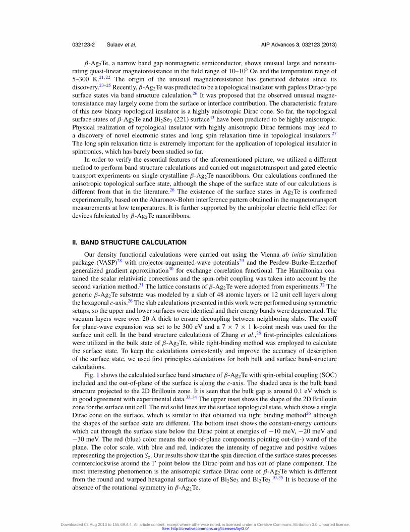
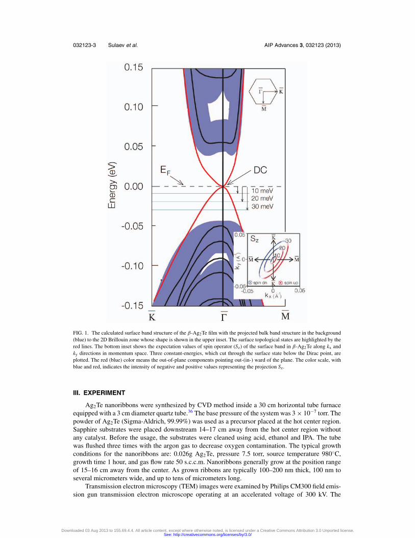
Fig. 1 shows the calculated surface band structure of β-Ag2Te with spin-orbital coupling (SOC)included and the out-of-plane of the surface is along the c-axis. The shaded area is the bulk bandstructure projected to the 2D Brillouin zone. It is seen that the bulk gap is around 0.1 eV which isin good agreement with experimental data.33, 34 The upper inset shows the shape of the 2D Brillouinzone for the surface unit cell. The red solid lines are the surface topological state, which show a singleDirac cone on the surface, which is similar to that obtained via tight binding method26 althoughthe shapes of the surface state are different. The bottom inset shows the constant-energy contourswhich cut through the surface state below the Dirac point at energies of −10 meV, −20 meV and−30 meV. The red (blue) color means the out-of-plane components pointing out-(in-) ward of theplane. The color scale, with blue and red, indicates the intensity of negative and positive valuesrepresenting the projection Sz. Our results show that the spin direction of the surface states precessescounterclockwise around the � point below the Dirac point and has out-of-plane component. Themost interesting phenomenon is the anisotropic surface Dirac cone of β-Ag2Te which is differentfrom the round and warped hexagonal surface state of Bi2Se3 and Bi2Te3.
10, 35 It is because of theabsence of the rotational symmetry in β-Ag2Te.
Downloaded 03 Aug 2013 to 155.69.4.4. All article content, except where otherwise noted, is licensed under a Creative Commons Attribution 3.0 Unported license.See: http://creativecommons.org/licenses/by/3.0/
032123-3 Sulaev et al. AIP Advances 3, 032123 (2013)
FIG. 1. The calculated surface band structure of the β-Ag2Te film with the projected bulk band structure in the background(blue) to the 2D Brillouin zone whose shape is shown in the upper inset. The surface topological states are highlighted by thered lines. The bottom inset shows the expectation values of spin operator (Sz) of the surface band in β-Ag2Te along kx andky directions in momentum space. Three constant-energies, which cut through the surface state below the Dirac point, areplotted. The red (blue) color means the out-of-plane components pointing out-(in-) ward of the plane. The color scale, withblue and red, indicates the intensity of negative and positive values representing the projection Sz.
III. EXPERIMENT
Ag2Te nanoribbons were synthesized by CVD method inside a 30 cm horizontal tube furnaceequipped with a 3 cm diameter quartz tube.36 The base pressure of the system was 3 × 10⁻⁷ torr. Thepowder of Ag2Te (Sigma-Aldrich, 99.99%) was used as a precursor placed at the hot center region.Sapphire substrates were placed downstream 14–17 cm away from the hot center region withoutany catalyst. Before the usage, the substrates were cleaned using acid, ethanol and IPA. The tubewas flushed three times with the argon gas to decrease oxygen contamination. The typical growthconditions for the nanoribbons are: 0.026g Ag2Te, pressure 7.5 torr, source temperature 980◦C,growth time 1 hour, and gas flow rate 50 s.c.c.m. Nanoribbons generally grow at the position rangeof 15–16 cm away from the center. As grown ribbons are typically 100–200 nm thick, 100 nm toseveral micrometers wide, and up to tens of micrometers long.
Transmission electron microscopy (TEM) images were examined by Philips CM300 field emis-sion gun transmission electron microscope operating at an accelerated voltage of 300 kV. The
Downloaded 03 Aug 2013 to 155.69.4.4. All article content, except where otherwise noted, is licensed under a Creative Commons Attribution 3.0 Unported license.See: http://creativecommons.org/licenses/by/3.0/
032123-4 Sulaev et al. AIP Advances 3, 032123 (2013)
5 1/nm
d(1 2 1) = 1.95
d(2 0 2) = 2.00
d(1 2 1) = 1.95
(2 0 2)
(1 2 1)
(1 2 1)
[1 0 1 ]
3 nm
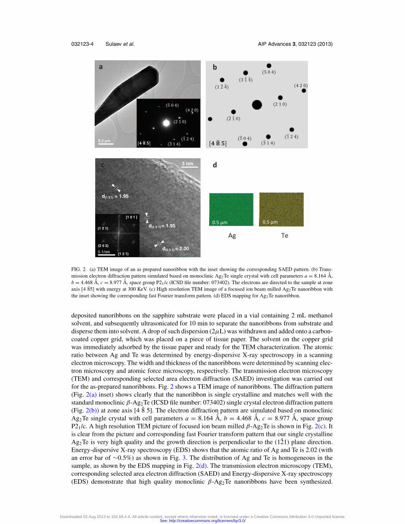
FIG. 2. (a) TEM image of an as prepared nanoribbon with the inset showing the corresponding SAED pattern. (b) Trans-mission electron diffraction pattern simulated based on monoclinic Ag2Te single crystal with cell parameters a = 8.164 Å,b = 4.468 Å, c = 8.977 Å, space group P21/c (ICSD file number: 073402). The electrons are directed to the sample at zoneaxis [4 85] with energy at 300 KeV. (c) High resolution TEM image of a focused ion beam milled Ag2Te nanoribbon withthe inset showing the corresponding fast Fourier transform pattern. (d) EDS mapping for Ag2Te nanoribbon.
deposited nanoribbons on the sapphire substrate were placed in a vial containing 2 mL methanolsolvent, and subsequently ultrasonicated for 10 min to separate the nanoribbons from substrate anddisperse them into solvent. A drop of such dispersion (2μL) was withdrawn and added onto a carbon-coated copper grid, which was placed on a piece of tissue paper. The solvent on the copper gridwas immediately adsorbed by the tissue paper and ready for the TEM characterization. The atomicratio between Ag and Te was determined by energy-dispersive X-ray spectroscopy in a scanningelectron microscopy. The width and thickness of the nanoribbons were determined by scanning elec-tron microscopy and atomic force microscopy, respectively. The transmission electron microscopy(TEM) and corresponding selected area electron diffraction (SAED) investigation was carried outfor the as-prepared nanoribbons. Fig. 2 shows a TEM image of nanoribbons. The diffraction pattern(Fig. 2(a) inset) shows clearly that the nanoribbon is single crystalline and matches well with thestandard monoclinic β-Ag2Te (ICSD file number: 073402) single crystal electron diffraction pattern(Fig. 2(b)) at zone axis [4 8 5]. The electron diffraction pattern are simulated based on monoclinicAg2Te single crystal with cell parameters a = 8.164 Å, b = 4.468 Å, c = 8.977 Å, space groupP21/c. A high resolution TEM picture of focused ion beam milled β-Ag2Te is shown in Fig. 2(c). Itis clear from the picture and corresponding fast Fourier transform pattern that our single crystallineAg2Te is very high quality and the growth direction is perpendicular to the (121) plane direction.Energy-dispersive X-ray spectroscopy (EDS) shows that the atomic ratio of Ag and Te is 2.02 (withan error bar of ∼0.5%) as shown in Fig. 3. The distribution of Ag and Te is homogeneous in thesample, as shown by the EDS mapping in Fig. 2(d). The transmission electron microscopy (TEM),corresponding selected area electron diffraction (SAED) and Energy-dispersive X-ray spectroscopy(EDS) demonstrate that high quality monoclinic β-Ag2Te nanoribbons have been synthesized.
Downloaded 03 Aug 2013 to 155.69.4.4. All article content, except where otherwise noted, is licensed under a Creative Commons Attribution 3.0 Unported license.See: http://creativecommons.org/licenses/by/3.0/
032123-5 Sulaev et al. AIP Advances 3, 032123 (2013)
0 1 2 3 4 50
20000
40000
TeL
r2T
eLr
TeL
b2
TeL
bT
eLa
TeL
nA
gLb2
TeL
lA
gLb
AgL
a
AgL
l
AlK
a
OK
a
Energy (keV)
Co
un
ts1 2 3 4 5
1.98
2.00
2.02
2.04
Ag
/Te
Mo
lar
Rat
io
Sample
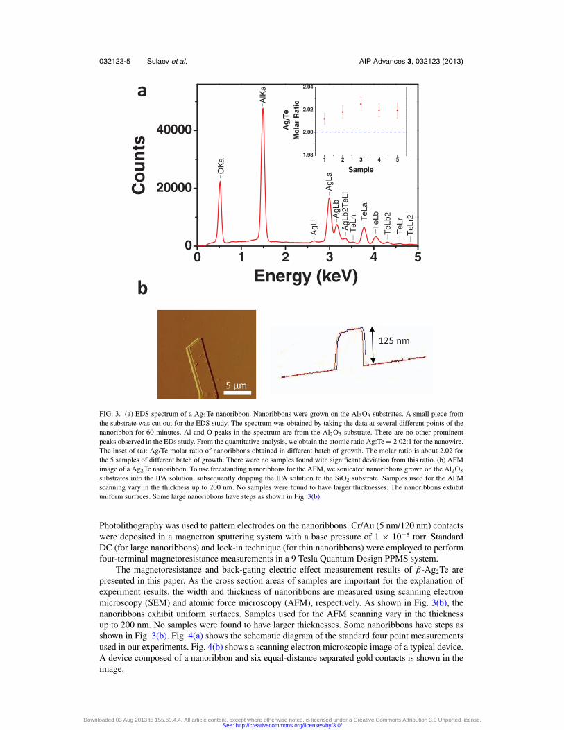
FIG. 3. (a) EDS spectrum of a Ag2Te nanoribbon. Nanoribbons were grown on the Al2O3 substrates. A small piece fromthe substrate was cut out for the EDS study. The spectrum was obtained by taking the data at several different points of thenanoribbon for 60 minutes. Al and O peaks in the spectrum are from the Al2O3 substrate. There are no other prominentpeaks observed in the EDs study. From the quantitative analysis, we obtain the atomic ratio Ag:Te = 2.02:1 for the nanowire.The inset of (a): Ag/Te molar ratio of nanoribbons obtained in different batch of growth. The molar ratio is about 2.02 forthe 5 samples of different batch of growth. There were no samples found with significant deviation from this ratio. (b) AFMimage of a Ag2Te nanoribbon. To use freestanding nanoribbons for the AFM, we sonicated nanoribbons grown on the Al2O3
substrates into the IPA solution, subsequently dripping the IPA solution to the SiO2 substrate. Samples used for the AFMscanning vary in the thickness up to 200 nm. No samples were found to have larger thicknesses. The nanoribbons exhibituniform surfaces. Some large nanoribbons have steps as shown in Fig. 3(b).
Photolithography was used to pattern electrodes on the nanoribbons. Cr/Au (5 nm/120 nm) contactswere deposited in a magnetron sputtering system with a base pressure of 1 × 10⁻⁸ torr. StandardDC (for large nanoribbons) and lock-in technique (for thin nanoribbons) were employed to performfour-terminal magnetoresistance measurements in a 9 Tesla Quantum Design PPMS system.
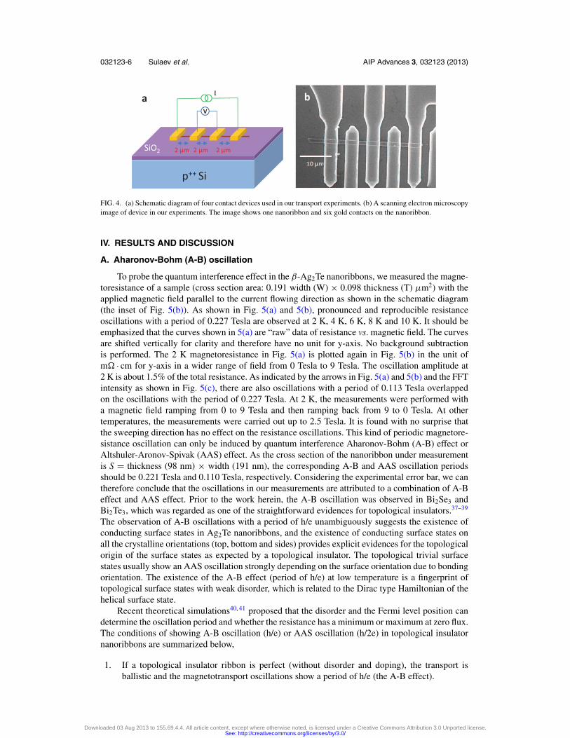
The magnetoresistance and back-gating electric effect measurement results of β-Ag2Te arepresented in this paper. As the cross section areas of samples are important for the explanation ofexperiment results, the width and thickness of nanoribbons are measured using scanning electronmicroscopy (SEM) and atomic force microscopy (AFM), respectively. As shown in Fig. 3(b), thenanoribbons exhibit uniform surfaces. Samples used for the AFM scanning vary in the thicknessup to 200 nm. No samples were found to have larger thicknesses. Some nanoribbons have steps asshown in Fig. 3(b). Fig. 4(a) shows the schematic diagram of the standard four point measurementsused in our experiments. Fig. 4(b) shows a scanning electron microscopic image of a typical device.A device composed of a nanoribbon and six equal-distance separated gold contacts is shown in theimage.
Downloaded 03 Aug 2013 to 155.69.4.4. All article content, except where otherwise noted, is licensed under a Creative Commons Attribution 3.0 Unported license.See: http://creativecommons.org/licenses/by/3.0/
032123-6 Sulaev et al. AIP Advances 3, 032123 (2013)
FIG. 4. (a) Schematic diagram of four contact devices used in our transport experiments. (b) A scanning electron microscopyimage of device in our experiments. The image shows one nanoribbon and six gold contacts on the nanoribbon.
IV. RESULTS AND DISCUSSION
A. Aharonov-Bohm (A-B) oscillation
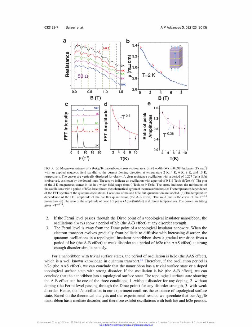
To probe the quantum interference effect in the β-Ag2Te nanoribbons, we measured the magne-toresistance of a sample (cross section area: 0.191 width (W) × 0.098 thickness (T) μm2) with theapplied magnetic field parallel to the current flowing direction as shown in the schematic diagram(the inset of Fig. 5(b)). As shown in Fig. 5(a) and 5(b), pronounced and reproducible resistanceoscillations with a period of 0.227 Tesla are observed at 2 K, 4 K, 6 K, 8 K and 10 K. It should beemphasized that the curves shown in 5(a) are “raw” data of resistance vs. magnetic field. The curvesare shifted vertically for clarity and therefore have no unit for y-axis. No background subtractionis performed. The 2 K magnetoresistance in Fig. 5(a) is plotted again in Fig. 5(b) in the unit ofm� · cm for y-axis in a wider range of field from 0 Tesla to 9 Tesla. The oscillation amplitude at2 K is about 1.5% of the total resistance. As indicated by the arrows in Fig. 5(a) and 5(b) and the FFTintensity as shown in Fig. 5(c), there are also oscillations with a period of 0.113 Tesla overlappedon the oscillations with the period of 0.227 Tesla. At 2 K, the measurements were performed witha magnetic field ramping from 0 to 9 Tesla and then ramping back from 9 to 0 Tesla. At othertemperatures, the measurements were carried out up to 2.5 Tesla. It is found with no surprise thatthe sweeping direction has no effect on the resistance oscillations. This kind of periodic magnetore-sistance oscillation can only be induced by quantum interference Aharonov-Bohm (A-B) effect orAltshuler-Aronov-Spivak (AAS) effect. As the cross section of the nanoribbon under measurementis S = thickness (98 nm) × width (191 nm), the corresponding A-B and AAS oscillation periodsshould be 0.221 Tesla and 0.110 Tesla, respectively. Considering the experimental error bar, we cantherefore conclude that the oscillations in our measurements are attributed to a combination of A-Beffect and AAS effect. Prior to the work herein, the A-B oscillation was observed in Bi2Se3 andBi2Te3, which was regarded as one of the straightforward evidences for topological insulators.37–39
The observation of A-B oscillations with a period of h/e unambiguously suggests the existence ofconducting surface states in Ag2Te nanoribbons, and the existence of conducting surface states onall the crystalline orientations (top, bottom and sides) provides explicit evidences for the topologicalorigin of the surface states as expected by a topological insulator. The topological trivial surfacestates usually show an AAS oscillation strongly depending on the surface orientation due to bondingorientation. The existence of the A-B effect (period of h/e) at low temperature is a fingerprint oftopological surface states with weak disorder, which is related to the Dirac type Hamiltonian of thehelical surface state.
Recent theoretical simulations40, 41 proposed that the disorder and the Fermi level position candetermine the oscillation period and whether the resistance has a minimum or maximum at zero flux.The conditions of showing A-B oscillation (h/e) or AAS oscillation (h/2e) in topological insulatornanoribbons are summarized below,
1. If a topological insulator ribbon is perfect (without disorder and doping), the transport isballistic and the magnetotransport oscillations show a period of h/e (the A-B effect).
Downloaded 03 Aug 2013 to 155.69.4.4. All article content, except where otherwise noted, is licensed under a Creative Commons Attribution 3.0 Unported license.See: http://creativecommons.org/licenses/by/3.0/
032123-7 Sulaev et al. AIP Advances 3, 032123 (2013)
0.0 0.5 1.0 1.5 0 2 4 6 82.6
2.8
3.0
3.2
3.4b
50 Ω
B (T)
Res
ista
nce
10K
8K
6K4K
2K
0.22 T
a
T=2 K
B (T)
ρρ ρρ(m
ΩΩ ΩΩcm
)
0 5 10 15 20 2 4 6 8 10 2 4 6 8 100.0
0.4
0.8
1.2
1.6ed
2K
4K
6K
8K
10K
FF
T In
ten
sity
F (T-1)
c
T-0.5
FF
T A
mp
litu
de
T(K)
T-0.38
Rat
io o
f p
eak
Am
plit
ud
es
T(K)
FIG. 5. (a) Magnetoresistance of a β-Ag2Te nanoribbon (cross section area: 0.191 width (W) × 0.098 thickness (T) μm2)with an applied magnetic field parallel to the current flowing direction at temperature 2 K, 4 K, 6 K, 8 K, and 10 K,respectively. The curves are vertically displaced for clarity. A clear resistance oscillation with a period of 0.227 Tesla (h/e)is observed, as shown by the dotted lines. The arrows indicate an oscillation with a period of 0.113 Tesla (h/2e). (b) The plotof the 2 K magnetoresistance in (a) in a wider field range from 0 Tesla to 9 Tesla. The arrow indicates the minimums ofthe oscillations with a period of h/2e. Inset shows the schematic diagram of the measurements. (c) The temperature dependenceof the FFT spectra of the quantum oscillations. Locations of h/e and h/2e flux quantization are labeled. (d) The temperaturedependence of the FFT amplitude of the h/e flux quantization (the A-B effect). The solid line is the curve of the T−0.5
power law. (e) The ratio of the amplitude of two FFT peaks (A(h/e)/A(h/2e) at different temperatures. The power law fittinggives ∼T−0.38.
2. If the Fermi level passes through the Dirac point of a topological insulator nanoribbon, theoscillations always show a period of h/e (the A-B effect) at any disorder strength.
3. The Fermi level is away from the Dirac point of a topological insulator nanowire. When theelectron transport evolves gradually from ballistic to diffusive with increasing disorder, thequantum oscillations in a topological insulator nanoribbon show a gradual transition from aperiod of h/e (the A-B effect) at weak disorder to a period of h/2e (the AAS effect) at strongenough disorder simultaneously.
For a nanoribbon with trivial surface states, the period of oscillation is h/2e (the AAS effect),which is a well known knowledge in quantum transport.45 Therefore, if the oscillation period ish/2e (the AAS effect), we can conclude that the nanoribbon has a trivial surface state or a dopedtopological surface state with strong disorder. If the oscillation is h/e (the A-B effect), we canconclude that the nanoribbon has a topological surface state. The topological surface state showingthe A-B effect can be one of the three conditions, 1. without disorder for any doping, 2. withoutdoping (the Fermi level passing through the Dirac point) for any disorder strength, 3. with weakdisorder. Hence, the h/e oscillation in our experiment confirms the existence of topological surfacestate. Based on the theoretical analysis and our experimental results, we speculate that our Ag2Tenanoribbon has a mediate disorder, and therefore exhibit oscillations with both h/e and h/2e periods.
Downloaded 03 Aug 2013 to 155.69.4.4. All article content, except where otherwise noted, is licensed under a Creative Commons Attribution 3.0 Unported license.See: http://creativecommons.org/licenses/by/3.0/
032123-8 Sulaev et al. AIP Advances 3, 032123 (2013)
The other possibility is that the surface state includes a dominating topological nontrivial part and aweak topological trivial part coming from band bending at the surface, which shows A-B oscillationswith a period of h/e and AAS oscillation with a period of h/2e, respectively.
Recently, quantum oscillations with a period of h/e were observed in InN nanowires, whichhave a topological trivial surface state due to band bending.42 However, the oscillations are causedby energy level splitting and therefore their magnitude does not decay with increasing magneticfield. The magnitude of oscillations for Ag2Te decays with increasing magnetic field, which is astandard characteristic of quantum interference induced oscillation. Therefore, the A-B oscillation(h/e period) in our measurements should be a fingerprint of topological surface state and not be thetype of oscillations in InN nanowire. The decaying speed of A-B or AAS oscillation with increasingmagnetic field is related to the thickness of the surface states. The decay of the oscillation magnitudewith increasing magnetic field in Ag2Te is faster than that in Bi2Se3, which may indicate thickersurface states in Ag2Te3. To study the evolution of the A-B and AAS oscillation with increasingtemperature, fast Fourier transform (FFT) was employed to analyze the derivative dR/dB. TheFFT intensity of 2 K, 4 K, 6 K, 8 K, and 10 K are plotted in Fig. 5(c), which clearly shows thecoexistence of the A-B oscillation (h/e) and the AAS oscillation (h/2e). As shown in Fig. 5(e),the ratio of the FFT intensity of the A-B oscillation and AAS oscillation decreases with increasingtemperature, which is larger than 1 at 2 K and 4 K and smaller than 1 at 6 K, 8 K, and 10 K. Thisphenomenon may be explained by the increasing electron and phonon scattering with increasingtemperature. As aforementioned, when the electron transport evolves gradually from ballistic todiffusive with increasing disorder or scattering, the quantum oscillation in topological insulatorwill show a gradual transition from h/e period (the A-B effect) to h/2e period (the AAS effect)simultaneously. Therefore, the ratio of the FFT intensity of the h/e and h/2e oscillation shoulddecrease with increasing temperature due to the increasing scattering. The power law fitting of thetemperature dependent ratio gives ∼T−0.38.
Due to the topological surface transport, β-Ag2Te nanoribbons actually form a two dimensionaltransport system. In a two dimensional electron system with high density electrons and weakelectron-electron interaction, the phase coherence time τφ ∼ h/kBT can be estimated from thethermal broadening of the Fermi-Dirac distribution. The oscillation amplitude is proportional tothe phase coherence length Lφ = (Dτφ)−1/2 ∼ T−1/2. In a realistic system, the impurity scatteringand phonon scattering can also affect the evolution of the phase coherence with temperature. Atvery low temperature regime, the scattering due to paramagnetic impurity limits the increase ofLφ with decreasing temperature and therefore generates a saturation behavior of Lφ (T). At hightemperature regime, the contribution of phonon scattering induces a faster decay of Lφ with increasingtemperature than the T−1/2 law. The temperature dependence of oscillation amplitude of the A-Boscillation in Bi2Se3 and Bi2Te3 nanowires shows a ∼T−1/2 power law behavior from 2 K to20 K,37, 38 which indicates that the electron-electron interaction is dominated in the temperatureregime in their samples. In the A-B effect of Bi2Te3 nanoflake,39 the decay of oscillation withincreasing temperature is faster than the T−1/2 power law. As shown in Fig. 5(d), the decay of theFFT amplitude with increasing temperature of the β-Ag2Te sample is compared with the T−1/2 powerlaw between 2 K and 10 K. There is no sign of saturation at 2 K, which shows that the impurityscattering effect is still negligible at this temperature. This may indicate the high quality of oursample. At 8 K and 10 K, it can be observed that the FFT amplitudes start deviating from the T−1/2
law. The faster decay of FFT amplitude at 8 K and 10 K indicates the effect of inelastic phononscattering. As the temperature dependence of the FFT amplitudes of the quantum oscillations ofBi2Se3 and Bi2Te3 nanowires agrees with the T−1/2 power law up to 20 K, we may conclude thatthe phonon scattering effect is stronger in β-Ag2Te nanoribbons than that in Bi2Se3 and Bi2Te3
nanowires.
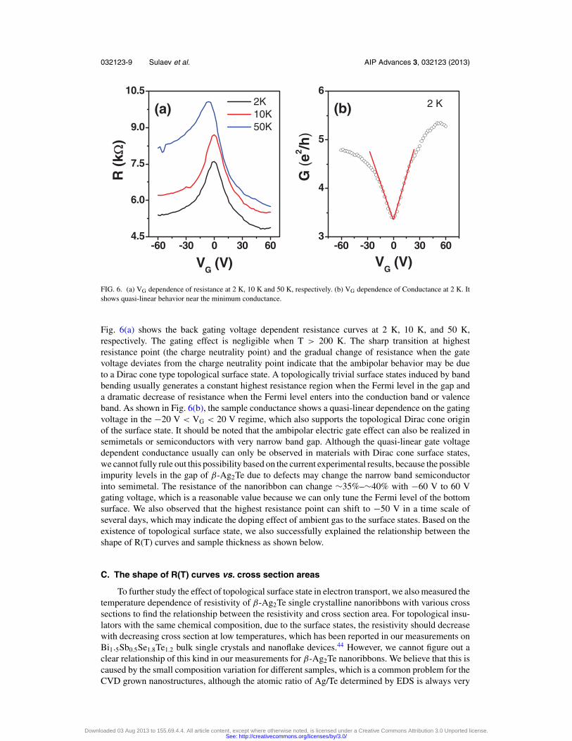
B. Ambipolar electric gate effect
For a nanoribbon with topological surface states composed of Dirac cone, an ambipolar electricfield effect with a sharp charge neutrality point should be expected. Pronounced ambipolar electricfield effect was observed in back-gated device fabricated by a 112 nm thick β-Ag2Te nanoribbon.
Downloaded 03 Aug 2013 to 155.69.4.4. All article content, except where otherwise noted, is licensed under a Creative Commons Attribution 3.0 Unported license.See: http://creativecommons.org/licenses/by/3.0/
032123-9 Sulaev et al. AIP Advances 3, 032123 (2013)
-60 -30 0 30 604.5
6.0
7.5
9.0
10.5 2K 10K 50K
R (
k)
VG (V)
(a)
-60 -30 0 30 603
4
5
6
G(e
2 /h)
VG (V)
2 K(b)
FIG. 6. (a) VG dependence of resistance at 2 K, 10 K and 50 K, respectively. (b) VG dependence of Conductance at 2 K. Itshows quasi-linear behavior near the minimum conductance.
Fig. 6(a) shows the back gating voltage dependent resistance curves at 2 K, 10 K, and 50 K,respectively. The gating effect is negligible when T > 200 K. The sharp transition at highestresistance point (the charge neutrality point) and the gradual change of resistance when the gatevoltage deviates from the charge neutrality point indicate that the ambipolar behavior may be dueto a Dirac cone type topological surface state. A topologically trivial surface states induced by bandbending usually generates a constant highest resistance region when the Fermi level in the gap anda dramatic decrease of resistance when the Fermi level enters into the conduction band or valenceband. As shown in Fig. 6(b), the sample conductance shows a quasi-linear dependence on the gatingvoltage in the −20 V < VG < 20 V regime, which also supports the topological Dirac cone originof the surface state. It should be noted that the ambipolar electric gate effect can also be realized insemimetals or semiconductors with very narrow band gap. Although the quasi-linear gate voltagedependent conductance usually can only be observed in materials with Dirac cone surface states,we cannot fully rule out this possibility based on the current experimental results, because the possibleimpurity levels in the gap of β-Ag2Te due to defects may change the narrow band semiconductorinto semimetal. The resistance of the nanoribbon can change ∼35%–∼40% with −60 V to 60 Vgating voltage, which is a reasonable value because we can only tune the Fermi level of the bottomsurface. We also observed that the highest resistance point can shift to −50 V in a time scale ofseveral days, which may indicate the doping effect of ambient gas to the surface states. Based on theexistence of topological surface state, we also successfully explained the relationship between theshape of R(T) curves and sample thickness as shown below.
C. The shape of R(T) curves vs. cross section areas
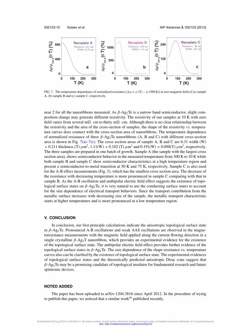
To further study the effect of topological surface state in electron transport, we also measured thetemperature dependence of resistivity of β-Ag2Te single crystalline nanoribbons with various crosssections to find the relationship between the resistivity and cross section area. For topological insu-lators with the same chemical composition, due to the surface states, the resistivity should decreasewith decreasing cross section at low temperatures, which has been reported in our measurements onBi1.5Sb0.5Se1.8Te1.2 bulk single crystals and nanoflake devices.44 However, we cannot figure out aclear relationship of this kind in our measurements for β-Ag2Te nanoribbons. We believe that this iscaused by the small composition variation for different samples, which is a common problem for theCVD grown nanostructures, although the atomic ratio of Ag/Te determined by EDS is always very
Downloaded 03 Aug 2013 to 155.69.4.4. All article content, except where otherwise noted, is licensed under a Creative Commons Attribution 3.0 Unported license.See: http://creativecommons.org/licenses/by/3.0/
032123-10 Sulaev et al. AIP Advances 3, 032123 (2013)
FIG. 7. The temperature dependence of normalized resistance (�ρ = ρ (T) − ρ (300 K)) at zero magnetic field of (a) sampleA, (b) sample B and (c) sample C, respectively.
near 2 for all the nanoribbons measured. As β-Ag2Te is a narrow band semiconductor, slight com-position change may generate different resistivity. The resistivity of our samples at 10 K with zerofield varies from several m� · cm to thirty m� · cm. Although there is no clear relationship betweenthe resistivity and the area of the cross-section of samples, the shape of the resistivity vs. tempera-ture curves does connect with the cross-section area of nanoribbons. The temperature dependenceof normalized resistance of three β-Ag2Te nanoribbons (A, B and C) with different cross-sectionarea is shown in Fig. 7(a)–7(c). The cross section areas of sample A, B and C are 6.31 width (W)× 0.211 thickness (T) μm2, 1.11(W) × 0.102 (T) μm2 and 0.191(W) × 0.098(T) μm2, respectively.The three samples are prepared in one batch of growth. Sample A (the sample with the largest crosssection area), shows semiconductor behavior in the measured temperature from 300 K to 10 K whileboth sample B and sample C show semiconductor characteristics at a high temperature region andpresent a semiconductor-to-metal transition at 50 K and 75 K, respectively. Sample C is also usedfor the A-B effect measurements (Fig. 5), which has the smallest cross section area. The decrease ofthe resistance with decreasing temperature is more pronounced in sample C comparing with that insample B. As the A-B oscillation and ambipolar electric field effect suggests the existence of topo-logical surface states on β-Ag2Te, it is very natural to use the conducting surface states to accountfor the size dependence of electrical transport behaviors. Since the transport contribution from themetallic surface increases with decreasing size of the sample, the metallic transport characteristicstarts at higher temperatures and is more pronounced at a low temperature region.
V. CONCLUSION
In conclusion, our first-principle calculations indicate the anisotropic topological surface statein β-Ag2Te. Pronounced A-B oscillations and weak AAS oscillations are observed in the magne-toresistance measurements with the magnetic field applied along the current flowing direction in asingle crystalline β-Ag2T nanoribbon, which provides an experimental evidence for the existenceof the topological surface state. The ambipolar electric field effect provides further evidence of thetopological surface states in β-Ag2Te. The size dependence of the shape resistance vs. temperaturecurves also can be clarified by the existence of topological surface state. The experimental evidencesof topological surface states and the theoretically predicted anisotropic Dirac cone suggest thatβ-Ag2Te may be a promising candidate of topological insulator for fundamental research and futurespintronic devices.
NOTED ADDED
The paper has been uploaded to arXiv:1204.3816 since April 2012. In the procedure of tryingto publish this paper, we noticed that a similar work46 published recently.
Downloaded 03 Aug 2013 to 155.69.4.4. All article content, except where otherwise noted, is licensed under a Creative Commons Attribution 3.0 Unported license.See: http://creativecommons.org/licenses/by/3.0/
032123-11 Sulaev et al. AIP Advances 3, 032123 (2013)
ACKNOWLEDGMENT
L. W. acknowledges the support from Singapore National Research Foundation (RCA-08/018)and MOE Tier 2 (MOE2010-T2-2-059). S. Q. S. thanks the Research Grant Council of Hong Kongunder Grant No. HKU705110P. W. G. Z. acknowledges the Singapore A*STAR SERC 102 1010019. T. Y. acknowledges NTU-SUG M4080513. The authors thank Hongming Weng and SergeyV. Eremeev for their helpful discussion.
1 J. E. Moore, Nature (London) 464, 194 (2010).2 M. Z. Hasan and C. L. Kane, Rev. Mod. Phys. 82, 3045 (2010).3 X. L. Qi and S. C. Zhang, Rev. Mod. Phys. 83, 1057 (2011).4 M. Konig, H. Buhmann, L. W. Molenkamp, T. L. Hughes, C. X. Liu, X. L. Qi, and S. C. Zhang, J. Phys. Soc. Jpn. 77,
031007 (2008).5 M. Konig, S. Wiedmann, C. Brune, A. Roth, H. Buhmann, L. W. Molenkamp, X. L. Qi, and S. C. Zhang, Science 318, 766
(2007).6 I. Knez, R. R. Du and G. Sullivan, Phys. Rev. Lett. 107, 136603 (2011).7 J. N. Hancock, J. L. M. van Mechelen, A. B. Kuzmenko, D. van der Marel, C. Brune, E. G. Novik, G. B. Astakhov, H.
Buhmann, and L. W. Molenkamp, Phys. Rev. Lett. 107, 136803 (2011).8 C. Brune, C. X. Liu, E. G. Novik, E. M. Hankiewicz, H. Buhmann, Y. L. Chen, X. L. Qi, Z. X. Shen, S. C. Zhang, and
L. W. Molenkamp, Phys. Rev. Lett. 106, 126803 (2011).9 Y. Xia, D. Dian, D. Hsieh, L. Wray, A. Pal, H. Lin, A. Bansil, D. Grauer, Y. S. Hor, R. J. Cava, and M. Z. Hasan, Nat.
Phys. 5, 398 (2009).10 Y. L. Chen, J. G. Analytis, J. H. Chu, Z. K. Liu, S. K. Mo, X. L. Qi, H. J. Zhang, D. H. Lu, X. Dai, Z. Fang, S. C. Zhang,
I. R. Fisher, Z. Hussain, and Z. X. Shen, Science 325, 178 (2009).11 D. Hsieh, Y. Xia, L. Wray, D. Qian, A. Pal, J. H. Dil, J. Osterwalder, F. Meier, G. Bihlmayer, C. L. Kane, Y. S. Hor, R. J.
Cava, and M. Z. Hasan, Science 323, 919 (2009).12 D. Hsieh, Y. Xia, D. Qian, L. Wray, J. H. Dil, F. Meier, J. Osterwalder, L. Patthey, J. G. Checkelsky, N. P. Ong, A. V.
Fedorov, H. Lin, A. Bansil, D. Grauer, Y. S. Hor, R. J. Cava, and M. Z. Hasan, Nature (London) 460, 1101 (2009).13 J. G. Analytis, J. H. Chu, Y. Chen, F. Corredor, R. D. McDonald, Z. X. Shen, and I. R. Fisher, Phys.Rev. B 81, 205407
(2010).14 Y. S. Hor, A. Richardella, P. Roushan, Y. Xia, J. G. Checkelsky, A. Yazdani, M. Z. Hasan, N. P. Ong, and R. J. Cava, Phys.
Rev. B 79, 195208 (2009).15 J. G. Checkelsky, Y. S. Hor, R. J. Cava, and N. P. Ong, Phys. Rev. Lett. 106, 196801 (2011).16 N. P. Butch, K. Kirshenbaum, P. Syers, A. B. Sushkov, G. S. Jenkins, H. D. Drew, and J. Paglione, Phys. Rev. B 81,
241301(R) (2010).17 J. Chen, H. J. Qin, F. Yang, J. Liu, T. Guan, F. M. Qu, G. H. Zhang, J. R. Shi, X. C. Xie, C. L. Yang, K. H. Wu, Y. Q. Li,
and L. Lu, Phys. Rev. Lett. 105, 176602 (2010).18 H. T. He, G. Wang, T. Zhang, I. K. Sou, G. K. L. Wong, J. N. Wang, H. Z. Lu, S. Q. Shen, and F. C. Zhang, Phys. Rev.
Lett. 106, 166805 (2011).19 S. Matsuo, T. Koyama, K. Shimamura, T. Arakawa, Y. Nishihara, D. Chiba, K. Kobayashi, T. Ono, C. Z. Chang, K. He, X.
C. Ma, and Q. K. Xue, Phys. Rev. B 85, 075440 (2012).20 J. Wang, A. M. DaSilva, C. Z. Chang, K. He, J. K. Jain, N. Samarth, X. C. Ma, Q. K. Xue, and M. H. W. Chan, Phys. Rev.
B 83, 245438 (2011).21 R. Xu, A. Husmann, T. F. Rosenbaum, M. L. Saboungi, J. E. Enderby, and P. B. Littlewood, Nature (London) 390, 57
(1997).22 A. Husmann, J. B. Betts, G. S. Boebinger, A. Migliori, T. F. Rosenbaum, and Saboungi M. L., Nature (London) 417, 421
(2002).23 A. A. Abrikosov, Phys. Rev. B 58, 2788 (1998).24 M. M. Parish and P. B. Littlewood, Nature (London) 426, 162 (2003).25 J. S. Hu and T. F. Rosenbaum, Nat. Mater. 7, 697–700 (2008).26 W. Zhang, R. Yu, W. X. Feng, Y. G. Yao, H. M. Weng, X. Dai, and Z. Fang, Phys. Rev. Lett. 106, 156808 (2011).27 V. E. Sackstedar IV, S. Kettemann, X. Dai, Q. S. Wu, and Z. Fang, arXiv:1108.2938v1 (2011).28 G. Kresse and J. Hafner, Phys. Rev. B 48, 13115 (1993).29 P. E. Blochl, Phys. Rev. B 50, 17953–17979 (1994).30 J. P. Perdew, K. Burke, and M. Ernzerhof, Phys. Rev. Lett. 77, 3865–3868 (1996).31 D. D. Koelling and B. N. Harmon, J. Phys. C: Solid Stat. Phys. 10, 3107 (1977).32 A. van der Lee and J. L. de Boer, Acta Cryst. C 49, 1444–1446 (1993).33 R. Dalven, Phys. Rev. Lett. 16, 311–312 (1966).34 R. Dalven and R. Gill, Phys. Rev. B 159, 645–649 (1967).35 L. Fu, Phys. Rev. Lett. 103, 266801 (2009).36 J. H. In, Y. D. Yoo, J. G. Kim, K. Y. Seo, H. J. Kim, H. Ihee, S. H. Oh, and B. S. Kim, Nano Lett. 10, 4501 (2010).37 H. Peng, K. Lai, D. Kong, S. Meister, Y. Chen, X.-L. Qi, S.-C. Zhang, Z.-X. Shen, and Y. Cui, Nat. Mater. 9, 225 (2010).38 F. X. Xiu, L. He, Y. Wang, L. Cheng, L. T. Chang, M. Lang, G. Huang, X. F. Kou, Y. Zhou, X. W. Jiang, Z. G. Chen, J.
Zou, A. Shailos, and K. L. Wang, Nat. Nano. 6, 216 (2011).39 Z. G. Li, Y. Y. Qin, F. Q. Song, Q. H. Wang, X. F. Wang, B. G. Wang, H. F. Ding, C. van Haesondonck, J. G. Wang, Y. H.
Zhang, G. H. Wang, Appl. Phys. Lett. 100, 083107 (2012).
Downloaded 03 Aug 2013 to 155.69.4.4. All article content, except where otherwise noted, is licensed under a Creative Commons Attribution 3.0 Unported license.See: http://creativecommons.org/licenses/by/3.0/
032123-12 Sulaev et al. AIP Advances 3, 032123 (2013)
40 Y. Zhang and A. Vishwanath, Phys. Rev. Lett. 105, 206601 (2010).41 J. H. Bardarson, P. W. Brouwer, and J. E. Moore, Phys. Rev. Lett. 105, 156803 (2010).42 T. Richer, C. Blomers, H. Luth, R. Calarco, M. Indlekofe, M. Marso, and T. Schapers, Nano Lett. 8, 2834 (2008).43 C. Y. Moon, J. H. Han, H. Lee, and H. J. Choi, Phys. Rev. B 84, 195425 (2011).44 B. Xia, P. Ren, A. Sulaev, P. Liu, S.-Q. Shen, L. Wang, Phys. Rev. B 87, 085442 (2013).45 V. F. Gantmakher, Electrons and Disorder in Solids (Oxford Science Publications, 2005).46 S. G. Lee, J. H. In, Y. D. Yoo, Y. G. Jo, Y. C. Park, H. J. Kim, H. C. Koo, J. Kim, B. S. Kim, and K. L. Wang, Nano Lett.
12, 4194 (2012).
Downloaded 03 Aug 2013 to 155.69.4.4. All article content, except where otherwise noted, is licensed under a Creative Commons Attribution 3.0 Unported license.See: http://creativecommons.org/licenses/by/3.0/