Excalibur Low-Noise, High-Speed, Precision - Texas Instruments
46
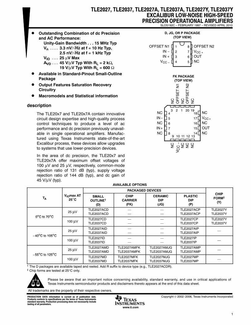
TLE2027, TLE2037, TLE2027A, TLE2037A, TLE2027Y, TLE2037Y EXCALIBUR LOW-NOISE HIGH-SPEED PRECISION OPERATIONAL AMPLIFIERS SLOS192C − FEBRUARY 1997 − REVISED APRIL 2010 1 D Outstanding Combination of dc Precision and AC Performance: Unity-Gain Bandwidth . . . 15 MHz Typ V n 3.3 nV/√Hz at f = 10 Hz Typ, . . . . . 2.5 nV/√Hz at f = 1 kHz Typ V IO 25 μV Max . . . . A VD 45 V/μV Typ With R L = 2 kΩ, . . . . 19 V/μV Typ With R L = 600 Ω D Available in Standard-Pinout Small-Outline Package D Output Features Saturation Recovery Circuitry D Macromodels and Statistical information description The TLE20x7 and TLE20x7A contain innovative circuit design expertise and high-quality process control techniques to produce a level of ac performance and dc precision previously unavail- able in single operational amplifiers. Manufac- tured using Texas Instruments state-of-the-art Excalibur process, these devices allow upgrades to systems that use lower-precision devices. In the area of dc precision, the TLE20x7 and TLE20x7A offer maximum offset voltages of 100 μV and 25 μV, respectively, common-mode rejection ratio of 131 dB (typ), supply voltage rejection ratio of 144 dB (typ), and dc gain of 45 V/μV (typ). AVAILABLE OPTIONS PACKAGED DEVICES CHIP T A V IO max AT 25°C SMALL OUTLINE † (D) CHIP CARRIER (FK) CERAMIC DIP (JG) PLASTIC DIP (P) CHIP FORM ‡ (Y) 0°C to 70°C 25 μV TLE2027ACD TLE2037ACD — — — — TLE2027ACP TLE2037ACP TLE2027Y TLE2037Y 0°C to 70°C 100 μV TLE2027CD TLE2037CD — — — — TLE2027CP TLE2037CP TLE2027Y TLE2037Y 40°C to 105°C 25 μV TLE2027AID TLE2037AID — — — — TLE2027AIP TLE2037AIP — − 40°C to 105°C 100 μV TLE2027ID TLE2037ID — — — — TLE2027IP TLE2037IP — 55°C to 125°C 25 μV TLE2027AMD TLE2037AMD TLE2027AMFK TLE2037AMFK TLE2027AMJG TLE2037AMJG TLE2027AMP TLE2037AMP — − 55°C to 125°C 100 μV TLE2027MD TLE2037MD TLE2027MFK TLE2037MFK TLE2027MJG TLE2037MJG TLE2027MP TLE2037MP — † The D packages are available taped and reeled. Add R suffix to device type (e.g., TLE2027ACDR). ‡ Chip forms are tested at 25°C only. Copyright © 2002−2006, Texas Instruments Incorporated PRODUCTION DATA information is current as of publication date. Products conform to specifications per the terms of Texas Instruments standard warranty. Production processing does not necessarily include testing of all parameters. Please be aware that an important notice concerning availability, standard warranty, and use in critical applications of Texas Instruments semiconductor products and disclaimers thereto appears at the end of this data sheet. All trademarks are the property of their respective owners. www.ti.com 1 2 3 4 8 7 6 5 OFFSET N1 IN − IN + V CC − OFFSET N2 V CC + OUT NC D, JG, OR P PACKAGE (TOP VIEW) 3 2 1 20 19 9 10 11 12 13 4 5 6 7 8 18 17 16 15 14 NC V CC + NC OUT NC NC IN − NC IN+ NC FK PACKAGE (TOP VIEW) NC OFFSET N1 NC NC NC NC NC NC OFFSET N2 CC − V
Transcript of Excalibur Low-Noise, High-Speed, Precision - Texas Instruments
TLE2027, TLE2037, TLE2027A, TLE2037A, TLE2027Y, TLE2037YEXCALIBUR LOW-NOISE HIGH-SPEED
PRECISION OPERATIONAL AMPLIFIERS
�
SLOS192C − FEBRUARY 1997 − REVISED APRIL 2010
1
� Outstanding Combination of dc Precisionand AC Performance:
Unity-Gain Bandwidth . . . 15 MHz TypVn 3.3 nV/√Hz at f = 10 Hz Typ,. . . . .
2.5 nV/√Hz at f = 1 kHz TypVIO 25 μV Max. . . .
AVD 45 V/μV Typ With RL = 2 kΩ,. . . .
19 V/μV Typ With RL = 600 Ω� Available in Standard-Pinout Small-Outline
Package
� Output Features Saturation RecoveryCircuitry
� Macromodels and Statistical information
description
The TLE20x7 and TLE20x7A contain innovativecircuit design expertise and high-quality processcontrol techniques to produce a level of acperformance and dc precision previously unavail-able in single operational amplifiers. Manufac-tured using Texas Instruments state-of-the-artExcalibur process, these devices allow upgradesto systems that use lower-precision devices.
In the area of dc precision, the TLE20x7 andTLE20x7A offer maximum offset voltages of100 μV and 25 μV, respectively, common-moderejection ratio of 131 dB (typ), supply voltagerejection ratio of 144 dB (typ), and dc gain of45 V/μV (typ).
AVAILABLE OPTIONS
PACKAGED DEVICESCHIP
TAVIOmax AT
25°CSMALL
OUTLINE†
(D)
CHIPCARRIER
(FK)
CERAMICDIP(JG)
PLASTICDIP(P)
CHIPFORM‡
(Y)
0°C to 70°C
25 μVTLE2027ACDTLE2037ACD
——
——
TLE2027ACPTLE2037ACP
TLE2027YTLE2037Y
0°C to 70°C100 μV
TLE2027CDTLE2037CD
——
——
TLE2027CPTLE2037CP
TLE2027YTLE2037Y
40°C to 105°C
25 μVTLE2027AIDTLE2037AID
——
——
TLE2027AIPTLE2037AIP
—
−40°C to 105°C100 μV
TLE2027IDTLE2037ID
——
——
TLE2027IPTLE2037IP
—
55°C to 125°C
25 μVTLE2027AMDTLE2037AMD
TLE2027AMFKTLE2037AMFK
TLE2027AMJGTLE2037AMJG
TLE2027AMPTLE2037AMP
—
−55°C to 125°C100 μV
TLE2027MDTLE2037MD
TLE2027MFKTLE2037MFK
TLE2027MJGTLE2037MJG
TLE2027MPTLE2037MP
—
† The D packages are available taped and reeled. Add R suffix to device type (e.g., TLE2027ACDR).‡ Chip forms are tested at 25°C only.
Copyright © 2002−2006, Texas Instruments IncorporatedPRODUCTION DATA information is current as of publication date.Products conform to specifications per the terms of Texas Instrumentsstandard warranty. Production processing does not necessarily includetesting of all parameters.
Please be aware that an important notice concerning availability, standard warranty, and use in critical applications ofTexas Instruments semiconductor products and disclaimers thereto appears at the end of this data sheet.
All trademarks are the property of their respective owners.
www.ti.com
1
2
3
4
8
7
6
5
OFFSET N1IN −IN +
VCC −
OFFSET N2VCC +OUTNC
D, JG, OR P PACKAGE(TOP VIEW)
3 2 1 20 19
9 10 11 12 13
4
5
6
7
8
18
17
16
15
14
NCVCC +
NCOUTNC
NCIN−NCIN+NC
FK PACKAGE(TOP VIEW)
NC
OF
FS
ET
N1
NC
NC
NC
NC
NC
NC
OF
FS
ET
N2
CC−
V
TLE2027, TLE2037, TLE2027A, TLE2037A, TLE2027Y, TLE2037YEXCALIBUR LOW-NOISE HIGH-SPEEDPRECISION OPERATIONAL AMPLIFIERS
�
SLOS192C − FEBRUARY 1997 − REVISED APRIL 2010
2 POST OFFICE BOX 655303 • DALLAS, TEXAS 75265POST OFFICE BOX 1443 • HOUSTON, TEXAS 77251−1443
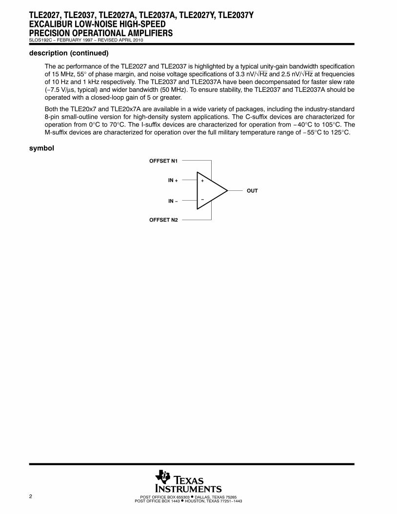
description (continued)
The ac performance of the TLE2027 and TLE2037 is highlighted by a typical unity-gain bandwidth specificationof 15 MHz, 55° of phase margin, and noise voltage specifications of 3.3 nV/√Hz and 2.5 nV/√Hz at frequenciesof 10 Hz and 1 kHz respectively. The TLE2037 and TLE2037A have been decompensated for faster slew rate(−7.5 V/μs, typical) and wider bandwidth (50 MHz). To ensure stability, the TLE2037 and TLE2037A should beoperated with a closed-loop gain of 5 or greater.
Both the TLE20x7 and TLE20x7A are available in a wide variety of packages, including the industry-standard8-pin small-outline version for high-density system applications. The C-suffix devices are characterized foroperation from 0°C to 70°C. The I-suffix devices are characterized for operation from −40°C to 105°C. TheM-suffix devices are characterized for operation over the full military temperature range of −55°C to 125°C.
symbol
OUT
OFFSET N2
IN −
IN +
OFFSET N1
−
+
TLE2027, TLE2037, TLE2027A, TLE2037A, TLE2027Y, TLE2037YEXCALIBUR LOW-NOISE HIGH-SPEED
PRECISION OPERATIONAL AMPLIFIERS
�
SLOS192C − FEBRUARY 1997 − REVISED APRIL 2010
3
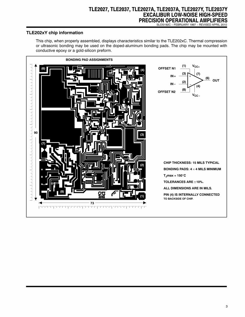
TLE202xY chip information
This chip, when properly assembled, displays characteristics similar to the TLE202xC. Thermal compressionor ultrasonic bonding may be used on the doped-aluminum bonding pads. The chip may be mounted withconductive epoxy or a gold-silicon preform.
BONDING PAD ASSIGNMENTS
CHIP THICKNESS: 15 MILS TYPICAL
BONDING PADS: 4 × 4 MILS MINIMUM
TJmax = 150°C
TOLERANCES ARE ±10%.
ALL DIMENSIONS ARE IN MILS.
PIN (4) IS INTERNALLY CONNECTEDTO BACKSIDE OF CHIP.
(1) (2) (3)
(4)
(5)
(6)(7)(8)
90
73
(1)
(2)
(3)
(4)(6)
(7)
(8)
+
−OUT
IN+
IN−
VCC+
VCC−
OFFSET N1
OFFSET N2
(1)
(3)
(2)
(8)
(7)
(4)
(6)
��������4��������4��������4��������4��������4�������
SLOS192C − FEBRUARY 1997 − REVISED APRIL 2010
���� ���4������ ��4� ������������ � ��4����� ���4��� � ���
4 www.ti.com
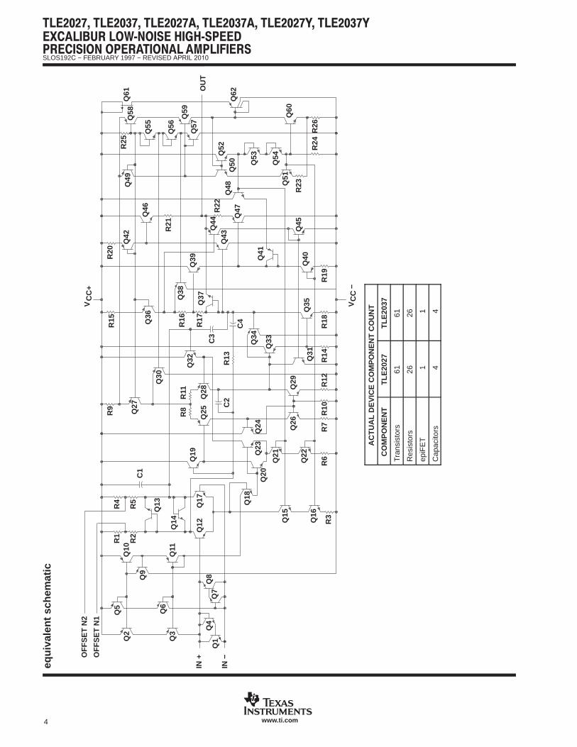
equi
vale
nt s
chem
atic
IN−
IN+
R24
R26
Q57
Q56
Q55
Q60
OU
T
Q62
Q59
Q61
Q58
R25
Q48
Q54
Q53Q
52
Q49
Q50
R23
R22
R21
R20
Q46
Q42
R19
Q47
Q44
Q43
Q40
Q45
Q41
Q39
Q38
Q37
Q35
R15 Q36
R16
R17
C4
C3
R13
Q34
Q33
Q32
R9 Q27
Q30
R8
R11
Q25
Q28
C2
Q31
Q26
Q29
R18
R14
R12
R10
R7
Q19
C1
Q24
Q23
Q20
R6
R3
Q21
Q22
Q16
Q15
Q18
R5
R4
Q13
Q14
Q17
R2
R1
OFF
SET
N2
OFF
SET
N1
Q12
Q10
Q9
Q11
Q8
Q7
Q5 Q6
Q4
Q1Q
3
Q2
Q51
CC
V
CC
+V
−
ACTU
AL D
EVIC
E C
OM
PON
ENT
CO
UN
TC
OM
PON
ENT
TLE2
027
TLE2
037
Tran
sist
ors
6161
Res
isto
rs26
26
epiF
ET
11
Cap
acito
rs4
4
TLE2027, TLE2037, TLE2027A, TLE2037A, TLE2027Y, TLE2037YEXCALIBUR LOW-NOISE HIGH-SPEED
PRECISION OPERATIONAL AMPLIFIERS
�
SLOS192C − FEBRUARY 1997 − REVISED APRIL 2010
5www.ti.com
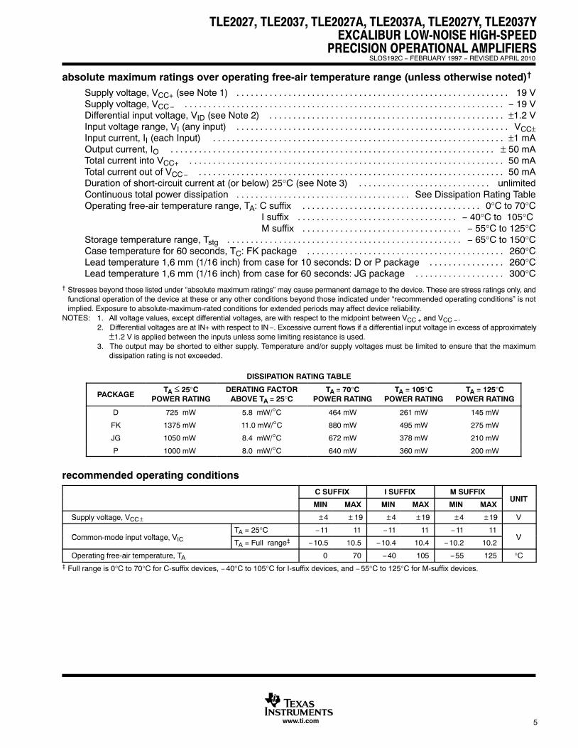
absolute maximum ratings over operating free-air temperature range (unless otherwise noted)†
Supply voltage, VCC+ (see Note 1) 19 V. . . . . . . . . . . . . . . . . . . . . . . . . . . . . . . . . . . . . . . . . . . . . . . . . . . . . . . . . . Supply voltage, VCC− − 19 V. . . . . . . . . . . . . . . . . . . . . . . . . . . . . . . . . . . . . . . . . . . . . . . . . . . . . . . . . . . . . . . . . . . . Differential input voltage, VID (see Note 2) ±1.2 V. . . . . . . . . . . . . . . . . . . . . . . . . . . . . . . . . . . . . . . . . . . . . . . . . . Input voltage range, VI (any input) VCC±. . . . . . . . . . . . . . . . . . . . . . . . . . . . . . . . . . . . . . . . . . . . . . . . . . . . . . . . . . Input current, II (each Input) ±1 mA. . . . . . . . . . . . . . . . . . . . . . . . . . . . . . . . . . . . . . . . . . . . . . . . . . . . . . . . . . . . . . Output current, IO ± 50 mA. . . . . . . . . . . . . . . . . . . . . . . . . . . . . . . . . . . . . . . . . . . . . . . . . . . . . . . . . . . . . . . . . . . . . Total current into VCC+ 50 mA. . . . . . . . . . . . . . . . . . . . . . . . . . . . . . . . . . . . . . . . . . . . . . . . . . . . . . . . . . . . . . . . . . . Total current out of VCC− 50 mA. . . . . . . . . . . . . . . . . . . . . . . . . . . . . . . . . . . . . . . . . . . . . . . . . . . . . . . . . . . . . . . . . Duration of short-circuit current at (or below) 25°C (see Note 3) unlimited. . . . . . . . . . . . . . . . . . . . . . . . . . . . Continuous total power dissipation See Dissipation Rating Table. . . . . . . . . . . . . . . . . . . . . . . . . . . . . . . . . . . . . Operating free-air temperature range, TA: C suffix 0°C to 70°C. . . . . . . . . . . . . . . . . . . . . . . . . . . . . . . . . . . . . .
I suffix − 40°C to 105°C . . . . . . . . . . . . . . . . . . . . . . . . . . . . . . . . . . M suffix − 55°C to 125°C. . . . . . . . . . . . . . . . . . . . . . . . . . . . . . . . . .
Storage temperature range, Tstg − 65°C to 150°C. . . . . . . . . . . . . . . . . . . . . . . . . . . . . . . . . . . . . . . . . . . . . . . . . . Case temperature for 60 seconds, TC: FK package 260°C. . . . . . . . . . . . . . . . . . . . . . . . . . . . . . . . . . . . . . . . . . Lead temperature 1,6 mm (1/16 inch) from case for 10 seconds: D or P package 260°C. . . . . . . . . . . . . . . . Lead temperature 1,6 mm (1/16 inch) from case for 60 seconds: JG package 300°C. . . . . . . . . . . . . . . . . . .
† Stresses beyond those listed under “absolute maximum ratings” may cause permanent damage to the device. These are stress ratings only, andfunctional operation of the device at these or any other conditions beyond those indicated under “recommended operating conditions” is notimplied. Exposure to absolute-maximum-rated conditions for extended periods may affect device reliability.
NOTES: 1. All voltage values, except differential voltages, are with respect to the midpoint between VCC + and VCC − .2. Differential voltages are at IN+ with respect to IN−. Excessive current flows if a differential input voltage in excess of approximately
±1.2 V is applied between the inputs unless some limiting resistance is used.3. The output may be shorted to either supply. Temperature and/or supply voltages must be limited to ensure that the maximum
dissipation rating is not exceeded.
DISSIPATION RATING TABLE
PACKAGETA ≤ 25°C
POWER RATINGDERATING FACTOR
ABOVE TA = 25°CTA = 70°C
POWER RATINGTA = 105°C
POWER RATINGTA = 125°C
POWER RATING
D 725 mW 5.8 mW/°C 464 mW 261 mW 145 mW
FK 1375 mW 11.0 mW/°C 880 mW 495 mW 275 mW
JG 1050 mW 8.4 mW/°C 672 mW 378 mW 210 mW
P 1000 mW 8.0 mW/°C 640 mW 360 mW 200 mW
recommended operating conditions
C SUFFIX I SUFFIX M SUFFIXUNIT
MIN MAX MIN MAX MIN MAXUNIT
Supply voltage, VCC ± ±4 ± 19 ±4 ±19 ±4 ±19 V
Common mode input voltage VTA = 25°C −11 11 −11 11 −11 11
VCommon-mode input voltage, VIC TA = Full range‡ −10.5 10.5 −10.4 10.4 −10.2 10.2V
Operating free-air temperature, TA 0 70 −40 105 −55 125 °C‡ Full range is 0°C to 70°C for C-suffix devices, −40°C to 105°C for I-suffix devices, and −55°C to 125°C for M-suffix devices.
TLE2027, TLE2037, TLE2027A, TLE2037A, TLE2027Y, TLE2037YEXCALIBUR LOW-NOISE HIGH-SPEEDPRECISION OPERATIONAL AMPLIFIERS
�
SLOS192C − FEBRUARY 1997 − REVISED APRIL 2010
6 www.ti.com
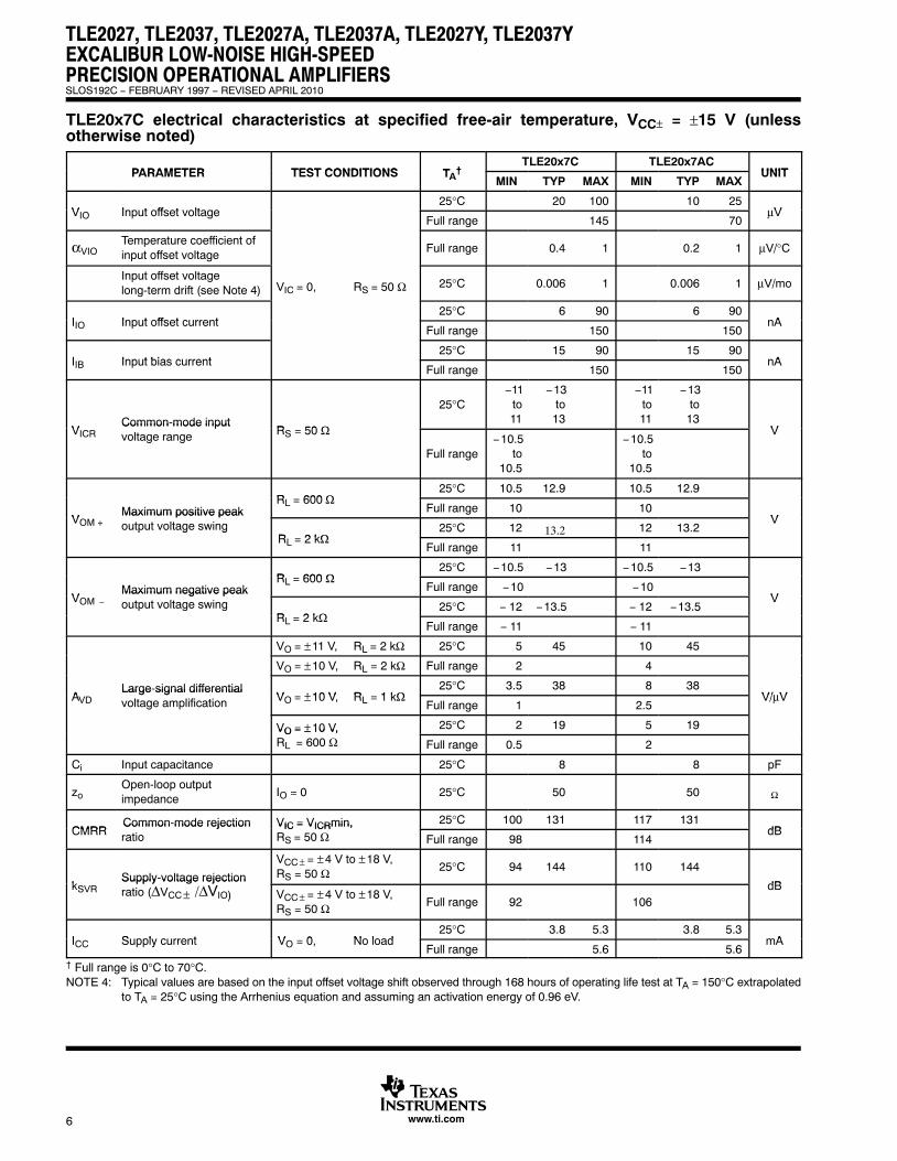
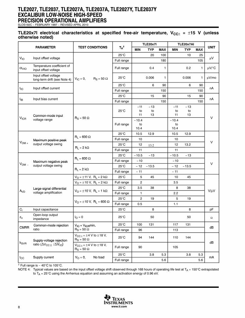
TLE20x7C electrical characteristics at specified free-air temperature, VCC± = ±15 V (unlessotherwise noted)
PARAMETER TEST CONDITIONS T †TLE20x7C TLE20x7AC
UNITPARAMETER TEST CONDITIONS TA†
MIN TYP MAX MIN TYP MAXUNIT
V Input offset voltage25°C 20 100 10 25
VVIO Input offset voltageFull range 145 70
μV
αVIOTemperature coefficient ofinput offset voltage
Full range 0.4 1 0.2 1 μV/°C
Input offset voltagelong-term drift (see Note 4) VIC = 0, RS = 50 Ω 25°C 0.006 1 0.006 1 μV/mo
I Input offset current25°C 6 90 6 90
nAIIO Input offset currentFull range 150 150
nA
I Input bias current25°C 15 90 15 90
nAIIB Input bias currentFull range 150 150
nA
VCommon-mode input
R 50 Ω
25°C−11
to11
−13to13
−11to11
−13to
13VVICR
Common mode inputvoltage range RS = 50 Ω
Full range−10.5
to10.5
−10.5to
10.5
V
R 600 Ω25°C 10.5 12.9 10.5 12.9
V
Maximum positive peak
RL = 600 ΩFull range 10 10
VVOM +Maximum positive peakoutput voltage swing R 2 kΩ
25°C 12 13.2 12 13.2Vp g g
RL = 2 kΩFull range 11 11
R 600 Ω25°C −10.5 −13 −10.5 −13
VMaximum negative peak
RL = 600 ΩFull range −10 −10
VVOM −Maximum negative peakoutput voltage swing
R 2 kΩ25°C − 12 −13.5 − 12 −13.5
V
RL = 2 kΩFull range − 11 − 11
VO = ±11 V, RL = 2 kΩ 25°C 5 45 10 45
VO = ±10 V, RL = 2 kΩ Full range 2 4
ALarge-signal differential
V ±10 V R 1 kΩ25°C 3.5 38 8 38
V/ VAVDLarge signal differentialvoltage amplification VO = ±10 V, RL = 1 kΩ
Full range 1 2.5V/μV
VO = ±10 V, 25°C 2 19 5 19VO = ±10 V, RL = 600 Ω Full range 0.5 2
Ci Input capacitance 25°C 8 8 pF
zoOpen-loop output impedance
IO = 0 25°C 50 50 Ω
CMRRCommon-mode rejection VIC = VICRmin, 25°C 100 131 117 131
dBCMRRCommon mode rejectionratio
VIC = VICRmin,RS = 50 Ω Full range 98 114
dB
kSupply-voltage rejection
VCC ± = ±4 V to ±18 V,RS = 50 Ω 25°C 94 144 110 144
dBkSVRSupply voltage rejection ratio (ΔVCC ± /ΔVIO) VCC ± = ±4 V to ±18 V,
RS = 50 Ω Full range 92 106dB
I Supply current V 0 No load25°C 3.8 5.3 3.8 5.3
mAICC Supply current VO = 0, No loadFull range 5.6 5.6
mA
† Full range is 0°C to 70°C.NOTE 4: Typical values are based on the input offset voltage shift observed through 168 hours of operating life test at TA = 150°C extrapolated
to TA = 25°C using the Arrhenius equation and assuming an activation energy of 0.96 eV.
TLE2027, TLE2037, TLE2027A, TLE2037A, TLE2027Y, TLE2037YEXCALIBUR LOW-NOISE HIGH-SPEED
PRECISION OPERATIONAL AMPLIFIERS
�
SLOS192C − FEBRUARY 1997 − REVISED APRIL 2010
7www.ti.com
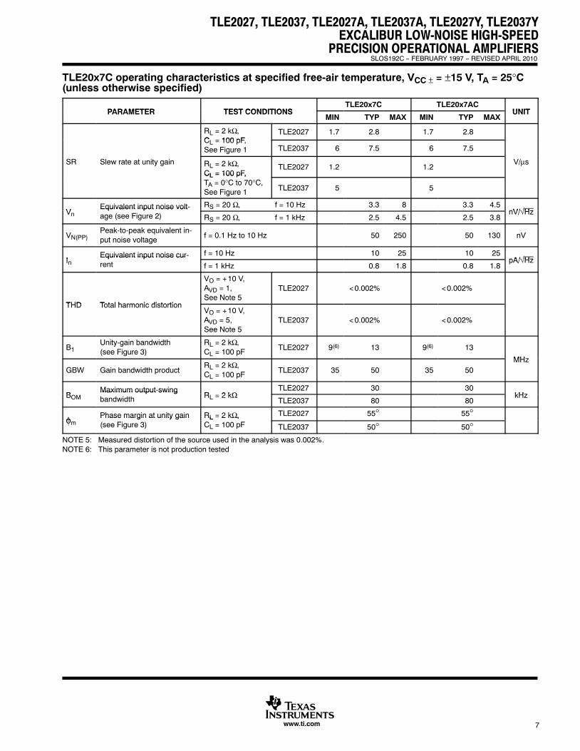
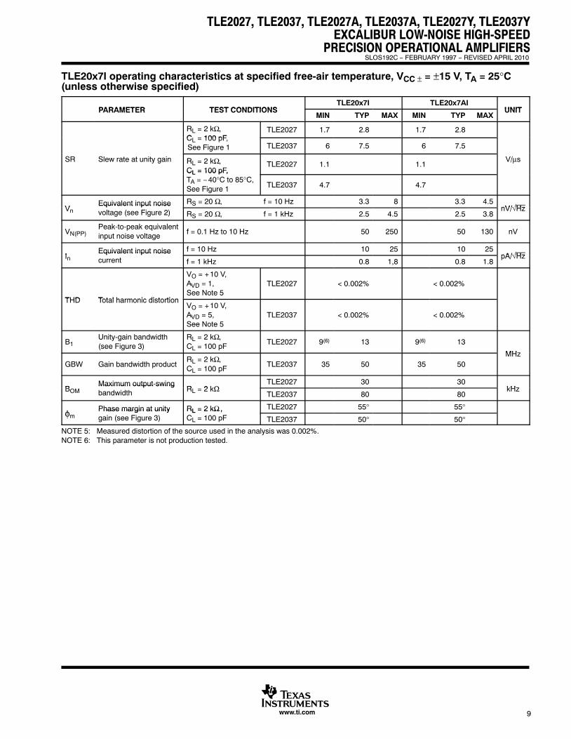
TLE20x7C operating characteristics at specified free-air temperature, VCC ± = ±15 V, TA = 25°C(unless otherwise specified)
PARAMETER TEST CONDITIONSTLE20x7C TLE20x7AC
UNITPARAMETER TEST CONDITIONSMIN TYP MAX MIN TYP MAX
UNIT
RL = 2 kΩ,C 100 pF
TLE2027 1.7 2.8 1.7 2.8CL = 100 pF,See Figure 1 TLE2037 6 7.5 6 7.5
SR Slew rate at unity gain RL = 2 kΩ,CL = 100 pF,
TLE2027 1.2 1.2V/μs
CL = 100 pF,TA = 0°C to 70°C,See Figure 1 TLE2037 5 5
VEquivalent input noise volt- RS = 20 Ω, f = 10 Hz 3.3 8 3.3 4.5
nV/√HzVnEquivalent input noise voltage (see Figure 2) RS = 20 Ω, f = 1 kHz 2.5 4.5 2.5 3.8
nV/√Hz
VN(PP)Peak-to-peak equivalent in-put noise voltage
f = 0.1 Hz to 10 Hz 50 250 50 130 nV
IEquivalent input noise cur- f = 10 Hz 10 25 10 25
pA/√HzInEquivalent input noise current f = 1 kHz 0.8 1.8 0.8 1.8
pA/√Hz
THD Total harmonic distortion
VO = +10 V,AVD = 1, See Note 5
TLE2027 <0.002% <0.002%
THD Total harmonic distortionVO = +10 V,AVD = 5, See Note 5
TLE2037 <0.002% <0.002%
B1Unity-gain bandwidth(see Figure 3)
RL = 2 kΩ,CL = 100 pF
TLE2027 9(6) 13 9(6) 13
MHzGBW Gain bandwidth product
RL = 2 kΩ,CL = 100 pF
TLE2037 35 50 35 50MHz
BMaximum output-swing
R 2 kΩTLE2027 30 30
kHzBOMMaximum output swingbandwidth RL = 2 kΩ
TLE2037 80 80kHz
φ Phase margin at unity gain RL = 2 kΩ, TLE2027 55° 55°φm
Phase margin at unity gain(see Figure 3)
RL 2 kΩ,CL = 100 pF TLE2037 50° 50°
NOTE 5: Measured distortion of the source used in the analysis was 0.002%.NOTE 6: This parameter is not production tested
TLE2027, TLE2037, TLE2027A, TLE2037A, TLE2027Y, TLE2037YEXCALIBUR LOW-NOISE HIGH-SPEEDPRECISION OPERATIONAL AMPLIFIERS
�
SLOS192C − FEBRUARY 1997 − REVISED APRIL 2010
8 www.ti.com
TLE20x7I electrical characteristics at specified free-air temperature, VCC± = ±15 V (unlessotherwise noted)
PARAMETER TEST CONDITIONS T †TLE20x7I TLE20x7AI
UNITPARAMETER TEST CONDITIONS TA†
MIN TYP MAX MIN TYP MAXUNIT
V Input offset voltage25°C 20 100 10 25
VVIO Input offset voltageFull range 180 105
μV
αVIOTemperature coefficient ofinput offset voltage
Full range 0.4 1 0.2 1 μV/°C
Input offset voltagelong-term drift (see Note 4) VIC = 0, RS = 50 Ω 25°C 0.006 1 0.006 1 μV/mo
I Input offset current25°C 6 90 6 90
nAIIO Input offset currentFull range 150 150
nA
I Input bias current25°C 15 90 15 90
nAIIB Input bias currentFull range 150 150
nA
VCommon-mode input
R 50 Ω
25°C−11
to11
−13to13
−11to11
−13to
13VVICR
Common mode input voltage range RS = 50 Ω
Full range−10.4
to10.4
−10.4to
10.4
V
R 600 Ω25°C 10.5 12.9 10.5 12.9
V
Maximum positive peak
RL = 600 ΩFull range 10 10
VVOM +Maximum positive peakoutput voltage swing R 2 kΩ
25°C 12 13.2 12 13.2Vp g g
RL = 2 kΩFull range 11 11
R 600 Ω25°C −10.5 −13 −10.5 −13
VMaximum negative peak
RL = 600 ΩFull range −10 −10
VVOM −Maximum negative peakoutput voltage swing
R 2 kΩ25°C − 12 −13.5 − 12 −13.5
V
RL = 2 kΩFull range − 11 − 11
VO = ±11 V, RL = 2 kΩ 25°C 5 45 10 45
VO = ±10 V, RL = 2 kΩ Full range 2 3.5
ALarge-signal differential
V ±10 V R 1 kΩ25°C 3.5 38 8 38
V/ VAVDLarge signal differentialvoltage amplification VO = ±10 V, RL = 1 kΩ
Full range 1 2.2V/μV
V ±10 V R 600 Ω25°C 2 19 5 19
VO = ±10 V, RL = 600 ΩFull range 0.5 1.1
Ci Input capacitance 25°C 8 8 pF
zoOpen-loop output impedance
IO = 0 25°C 50 50 Ω
CMRRCommon-mode rejection VIC = VICRmin, 25°C 100 131 117 131
dBCMRRCommon mode rejectionratio
VIC = VICRmin,RS = 50 Ω Full range 96 113
dB
kSupply-voltage rejection
VCC ± = ±4 V to ±18 V,RS = 50 Ω 25°C 94 144 110 144
dBkSVRSupply voltage rejection ratio (ΔVCC ± /ΔVIO) VCC ± = ±4 V to ±18 V,
RS = 50 Ω Full range 90 105dB
ICC Supply current VO 0 No load25°C 3.8 5.3 3.8 5.3
mAICC Supply current VO = 0, No loadFull range 5.6 5.6
mA
† Full range is − 40°C to 105°C.NOTE 4: Typical values are based on the input offset voltage shift observed through 168 hours of operating life test at TA = 150°C extrapolated
to TA = 25°C using the Arrhenius equation and assuming an activation energy of 0.96 eV.
TLE2027, TLE2037, TLE2027A, TLE2037A, TLE2027Y, TLE2037YEXCALIBUR LOW-NOISE HIGH-SPEED
PRECISION OPERATIONAL AMPLIFIERS
�
SLOS192C − FEBRUARY 1997 − REVISED APRIL 2010
9www.ti.com
TLE20x7I operating characteristics at specified free-air temperature, VCC ± = ±15 V, TA = 25°C(unless otherwise specified)
PARAMETER TEST CONDITIONSTLE20x7I TLE20x7AI
UNITPARAMETER TEST CONDITIONSMIN TYP MAX MIN TYP MAX
UNIT
RL = 2 kΩ,C 100 pF
TLE2027 1.7 2.8 1.7 2.8CL = 100 pF,See Figure 1 TLE2037 6 7.5 6 7.5
SR Slew rate at unity gain RL = 2 kΩ,CL = 100 pF,
TLE2027 1.1 1.1V/μs
CL = 100 pF,TA = −40°C to 85°C,See Figure 1 TLE2037 4.7 4.7
VEquivalent input noise RS = 20 Ω, f = 10 Hz 3.3 8 3.3 4.5
nV/√HzVnEquivalent input noisevoltage (see Figure 2) RS = 20 Ω, f = 1 kHz 2.5 4.5 2.5 3.8
nV/√Hz
VN(PP)Peak-to-peak equivalentinput noise voltage
f = 0.1 Hz to 10 Hz 50 250 50 130 nV
IEquivalent input noise f = 10 Hz 10 25 10 25
pA/√HzInEquivalent input noisecurrent f = 1 kHz 0.8 1,8 0.8 1.8
pA/√Hz
THD Total harmonic distortion
VO = +10 V, AVD = 1, See Note 5
TLE2027 < 0.002% < 0.002%
THD Total harmonic distortionVO = +10 V, AVD = 5, See Note 5
TLE2037 < 0.002% < 0.002%
B1Unity-gain bandwidth(see Figure 3)
RL = 2 kΩ,CL = 100 pF
TLE2027 9(6) 13 9(6) 13
MHzGBW Gain bandwidth product
RL = 2 kΩ,CL = 100 pF
TLE2037 35 50 35 50MHz
BMaximum output-swing
R 2 kΩTLE2027 30 30
kHzBOMMaximum output swingbandwidth RL = 2 kΩ
TLE2037 80 80kHz
φ Phase margin at unity RL = 2 kΩ , TLE2027 55° 55°φm
Phase margin at unitygain (see Figure 3)
RL = 2 kΩ ,CL = 100 pF TLE2037 50° 50°
NOTE 5: Measured distortion of the source used in the analysis was 0.002%.NOTE 6: This parameter is not production tested.
TLE2027, TLE2037, TLE2027A, TLE2037A, TLE2027Y, TLE2037YEXCALIBUR LOW-NOISE HIGH-SPEEDPRECISION OPERATIONAL AMPLIFIERS
�
SLOS192C − FEBRUARY 1997 − REVISED APRIL 2010
10 www.ti.com
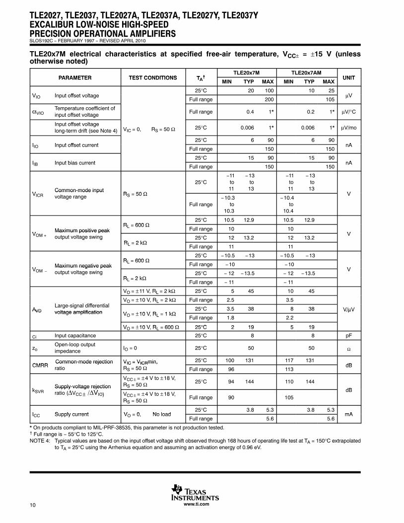
TLE20x7M electrical characteristics at specified free-air temperature, VCC± = ±15 V (unlessotherwise noted)
PARAMETER TEST CONDITIONS T †TLE20x7M TLE20x7AM
UNITPARAMETER TEST CONDITIONS TA†
MIN TYP MAX MIN TYP MAXUNIT
V Input offset voltage25°C 20 100 10 25
VVIO Input offset voltageFull range 200 105
μV
αVIOTemperature coefficient ofinput offset voltage
Full range 0.4 1* 0.2 1* μV/°C
Input offset voltagelong-term drift (see Note 4) VIC = 0, RS = 50 Ω 25°C 0.006 1* 0.006 1* μV/mo
I Input offset current25°C 6 90 6 90
nAIIO Input offset currentFull range 150 150
nA
I Input bias current25°C 15 90 15 90
nAIIB Input bias currentFull range 150 150
nA
VCommon-mode input
R 50 Ω
25°C−11
to11
−13to13
−11to11
−13to
13VVICR
Common mode inputvoltage range RS = 50 Ω
Full range−10.3
to10.3
−10.4to
10.4
V
R 600 Ω25°C 10.5 12.9 10.5 12.9
V
Maximum positive peak
RL = 600 ΩFull range 10 10
VVOM +Maximum positive peakoutput voltage swing R 2 kΩ
25°C 12 13.2 12 13.2Vp g g
RL = 2 kΩFull range 11 11
R 600 Ω25°C −10.5 −13 −10.5 −13
VMaximum negative peak
RL = 600 ΩFull range −10 −10
VVOM −Maximum negative peakoutput voltage swing
R 2 kΩ25°C − 12 −13.5 − 12 −13.5
V
RL = 2 kΩFull range − 11 − 11
VO = ±11 V, RL = 2 kΩ 25°C 5 45 10 45
L i l diff ti lVO = ±10 V, RL = 2 kΩ Full range 2.5 3.5
AVDLarge-signal differentialvoltage amplification V ±10 V R 1 kΩ
25°C 3.5 38 8 38 V/μVAVD voltage amplification VO = ±10 V, RL = 1 kΩFull range 1.8 2.2
V/μV
V ±10 V R 600 Ω 25°C 2 19 5 19VO = ±10 V, RL = 600 Ω 25°C 2 19 5 19
Ci Input capacitance 25°C 8 8 pF
zoOpen-loop output impedance
IO = 0 25°C 50 50 Ω
CMRRCommon-mode rejection VIC = VICRmin, 25°C 100 131 117 131
dBCMRRCommon mode rejectionratio
VIC = VICRmin,RS = 50 Ω Full range 96 113
dB
kSupply-voltage rejection
VCC ± = ±4 V to ±18 V,RS = 50 Ω 25°C 94 144 110 144
dBkSVRSupply voltage rejection ratio (ΔVCC ± /ΔVIO) VCC ± = ±4 V to ±18 V,
RS = 50 Ω Full range 90 105dB
I Supply current V 0 No load25°C 3.8 5.3 3.8 5.3
mAICC Supply current VO = 0, No loadFull range 5.6 5.6
mA
* On products compliant to MIL-PRF-38535, this parameter is not production tested.† Full range is − 55°C to 125°C.NOTE 4: Typical values are based on the input offset voltage shift observed through 168 hours of operating life test at TA = 150°C extrapolated
to TA = 25°C using the Arrhenius equation and assuming an activation energy of 0.96 eV.
TLE2027, TLE2037, TLE2027A, TLE2037A, TLE2027Y, TLE2037YEXCALIBUR LOW-NOISE HIGH-SPEED
PRECISION OPERATIONAL AMPLIFIERS
�
SLOS192C − FEBRUARY 1997 − REVISED APRIL 2010
11www.ti.com
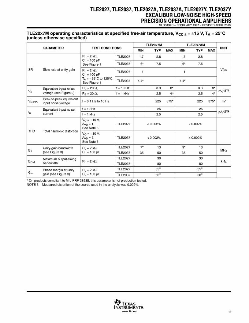
TLE20x7M operating characteristics at specified free-air temperature, VCC ± = ±15 V, TA = 25°C(unless otherwise specified)
PARAMETER TEST CONDITIONSTLE20x7M TLE20x7AM
UNITPARAMETER TEST CONDITIONSMIN TYP MAX MIN TYP MAX
UNIT
RL = 2 kΩ,C 100 pF
TLE2027 1.7 2.8 1.7 2.8CL = 100 pF,See Figure 1 TLE2037 6* 7.5 6* 7.5
SR Slew rate at unity gain RL = 2 kΩ,CL = 100 pF,
TLE2027 1 1V/μs
CL = 100 pF,TA = −55°C to 125°C,See Figure 1 TLE2037 4.4* 4.4*
VEquivalent input noise RS = 20 Ω, f = 10 Hz 3.3 8* 3.3 8*
nV/√HzVnEquivalent input noisevoltage (see Figure 2) RS = 20 Ω, f = 1 kHz 2.5 4* 2.5 4*
nV/√Hz
VN(PP)Peak-to-peak equivalentinput noise voltage
f = 0.1 Hz to 10 Hz 225 375* 225 375* nV
IEquivalent input noise f = 10 Hz 25 25
pA/√HzInEquivalent input noisecurrent f = 1 kHz 2.5 2.5
pA/√Hz
THD Total harmonic distortion
VO = +10 V,AVD = 1, See Note 5
TLE2027 < 0.002% < 0.002%
THD Total harmonic distortionVO = +10 V,AVD = 5, See Note 5
TLE2037 < 0.002% < 0.002%
BUnity-gain bandwidth RL = 2 kΩ, TLE2027 7* 13 9* 13
MHzB1Unity gain bandwidth(see Figure 3)
RL = 2 kΩ,CL = 100 pF TLE2037 35 50 35 50
MHz
BMaximum output-swing
R 2 kΩTLE2027 30 30
kHzBOMMaximum output swingbandwidth RL = 2 kΩ
TLE2037 80 80kHz
φ Phase margin at unity RL = 2 kΩ, TLE2027 55° 55°φm
Phase margin at unitygain (see Figure 3)
RL 2 kΩ,CL = 100 pF TLE2037 50° 50°
* On products compliant to MIL-PRF-38535, this parameter is not production tested.NOTE 5: Measured distortion of the source used in the analysis was 0.002%.
TLE2027, TLE2037, TLE2027A, TLE2037A, TLE2027Y, TLE2037YEXCALIBUR LOW-NOISE HIGH-SPEEDPRECISION OPERATIONAL AMPLIFIERS
�
SLOS192C − FEBRUARY 1997 − REVISED APRIL 2010
12 www.ti.com
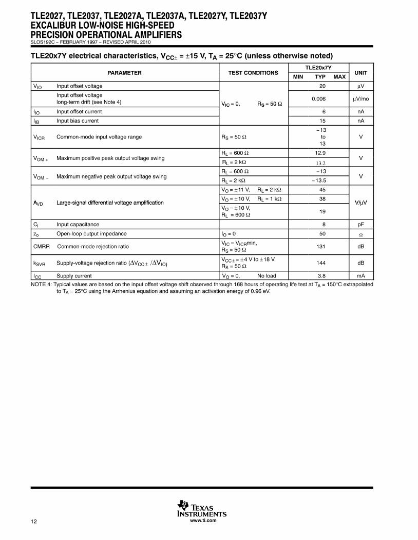
TLE20x7Y electrical characteristics, VCC± = ±15 V, TA = 25°C (unless otherwise noted)
PARAMETER TEST CONDITIONSTLE20x7Y
UNITPARAMETER TEST CONDITIONSMIN TYP MAX
UNIT
VIO Input offset voltage 20 μV
Input offset voltagelong-term drift (see Note 4) VIC = 0, RS = 50 Ω
0.006 μV/mo
IIO Input offset current
VIC = 0, RS = 50 Ω6 nA
IIB Input bias current 15 nA
VICR Common-mode input voltage range RS = 50 Ω−13
to13
V
V Maximum positive peak output voltage swingRL = 600 Ω 12.9
VVOM + Maximum positive peak output voltage swingRL = 2 kΩ 13.2
V
V Maximum negative peak output voltage swingRL = 600 Ω −13
VVOM − Maximum negative peak output voltage swingRL = 2 kΩ −13.5
V
VO = ±11 V, RL = 2 kΩ 45
AVD Large-signal differential voltage amplificationVO = ±10 V, RL = 1 kΩ 38
V/μVAVD Large-signal differential voltage amplificationVO = ±10 V, RL = 600 Ω 19
V/μV
Ci Input capacitance 8 pF
zo Open-loop output impedance IO = 0 50 Ω
CMRR Common-mode rejection ratioVIC = VICRmin,RS = 50 Ω 131 dB
kSVR Supply-voltage rejection ratio (ΔVCC ± /ΔVIO)VCC ± = ±4 V to ±18 V,RS = 50 Ω 144 dB
ICC Supply current VO = 0, No load 3.8 mA
NOTE 4: Typical values are based on the input offset voltage shift observed through 168 hours of operating life test at TA = 150°C extrapolatedto TA = 25°C using the Arrhenius equation and assuming an activation energy of 0.96 eV.
TLE2027, TLE2037, TLE2027A, TLE2037A, TLE2027Y, TLE2037YEXCALIBUR LOW-NOISE HIGH-SPEED
PRECISION OPERATIONAL AMPLIFIERS
�
SLOS192C − FEBRUARY 1997 − REVISED APRIL 2010
13www.ti.com
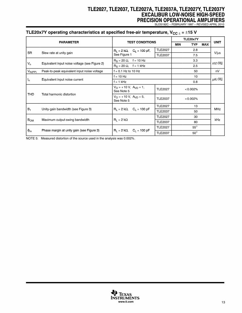
TLE20x7Y operating characteristics at specified free-air temperature, VCC ± = ±15 V
PARAMETER TEST CONDITIONSTLE20x7Y
UNITPARAMETER TEST CONDITIONSMIN TYP MAX
UNIT
SR Slew rate at unity gainRL = 2 kΩ, CL = 100 pF, TLE2027 2.8
V/ sSR Slew rate at unity gainRL = 2 kΩ, CL = 100 pF,See Figure 1 TLE2037 7.5
V/μs
V Equivalent input noise voltage (see Figure 2)RS = 20 Ω, f = 10 Hz 3.3
nV/√HzVn Equivalent input noise voltage (see Figure 2)RS = 20 Ω, f = 1 kHz 2.5
nV/√Hz
VN(PP) Peak-to-peak equivalent input noise voltage f = 0.1 Hz to 10 Hz 50 nV
I Equivalent input noise currentf = 10 Hz 10
pA/√HzIn Equivalent input noise currentf = 1 kHz 0.8
pA/√Hz
THD Total harmonic distortion
VO = +10 V, AVD = 1, See Note 5
TLE2027 <0.002%
THD Total harmonic distortionVO = +10 V, AVD = 5, See Note 5
TLE2037 <0.002%
B Unity gain bandwidth (see Figure 3) R 2 kΩ C 100 pFTLE2027 13
MHzB1 Unity-gain bandwidth (see Figure 3) RL = 2 kΩ, CL = 100 pFTLE2037 50
MHz
B Maximum output swing bandwidth R 2 kΩTLE2027 30
kHzBOM Maximum output-swing bandwidth RL = 2 kΩTLE2037 80
kHz
φ Phase margin at unity gain (see Figure 3) R 2 kΩ C 100 pFTLE2027 55°
φm Phase margin at unity gain (see Figure 3) RL = 2 kΩ, CL = 100 pFTLE2037 50°
NOTE 5: Measured distortion of the source used in the analysis was 0.002%.
TLE2027, TLE2037, TLE2027A, TLE2037A, TLE2027Y, TLE2037YEXCALIBUR LOW-NOISE HIGH-SPEEDPRECISION OPERATIONAL AMPLIFIERS
�
SLOS192C − FEBRUARY 1997 − REVISED APRIL 2010
14 www.ti.com
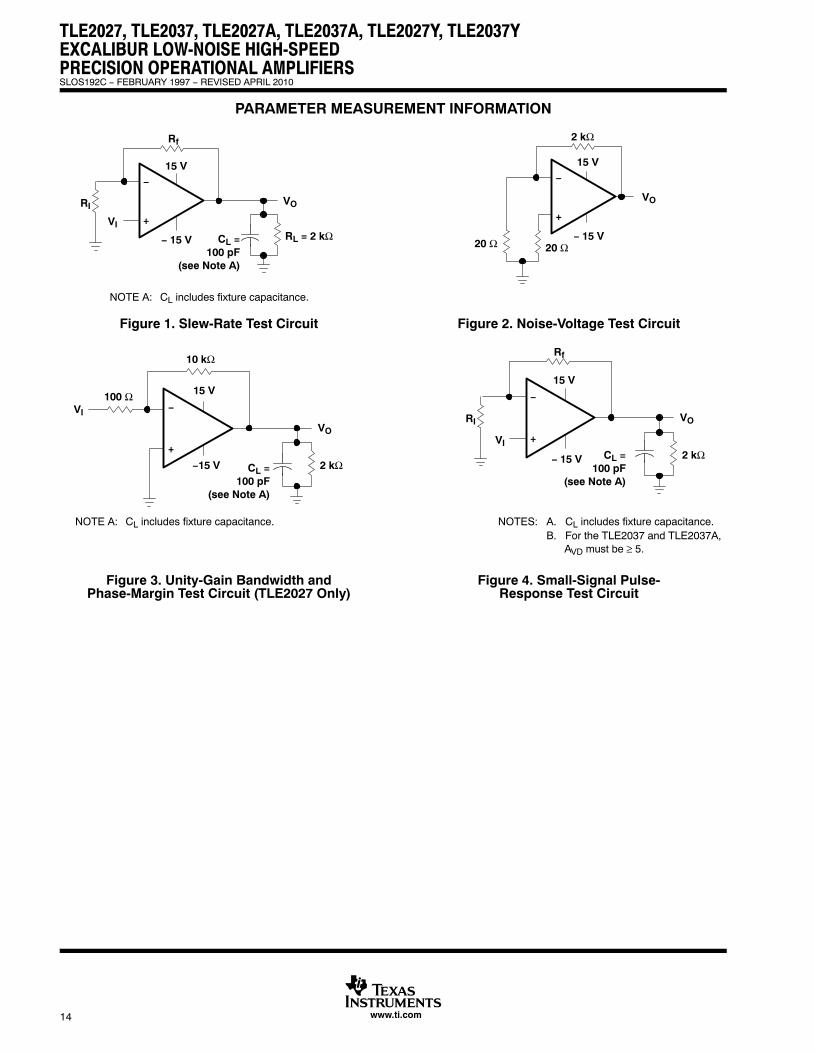
PARAMETER MEASUREMENT INFORMATION
VO
20 Ω20 Ω
2 kΩ
− 15 V
15 V
+
−
RL = 2 kΩCL =100 pF
(see Note A)
VO
− 15 V
VI +
−15 V
Rf
NOTE A: CL includes fixture capacitance.
RI
Figure 1. Slew-Rate Test Circuit Figure 2. Noise-Voltage Test Circuit
VO
2 kΩCL =100 pF
(see Note A)
10 kΩ
100 ΩVI
−15 V
15 V
+
−VO
2 kΩ− 15 V
15 V
−
+VICL =
100 pF(see Note A)
NOTES: A. CL includes fixture capacitance.NOTE A: CL includes fixture capacitance.B. For the TLE2037 and TLE2037A,
AVD must be ≥ 5.
Rf
RI
Figure 3. Unity-Gain Bandwidth and Figure 4. Small-Signal Pulse-Phase-Margin Test Circuit (TLE2027 Only) Response Test Circuit
TLE2027, TLE2037, TLE2027A, TLE2037A, TLE2027Y, TLE2037YEXCALIBUR LOW-NOISE HIGH-SPEED
PRECISION OPERATIONAL AMPLIFIERS
�
SLOS192C − FEBRUARY 1997 − REVISED APRIL 2010
15www.ti.com
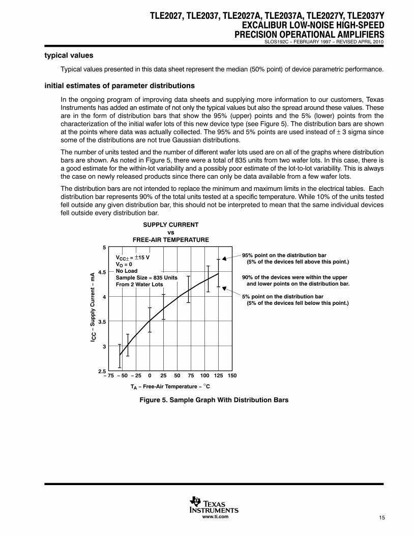
typical values
Typical values presented in this data sheet represent the median (50% point) of device parametric performance.
initial estimates of parameter distributions
In the ongoing program of improving data sheets and supplying more information to our customers, TexasInstruments has added an estimate of not only the typical values but also the spread around these values. Theseare in the form of distribution bars that show the 95% (upper) points and the 5% (lower) points from thecharacterization of the initial wafer lots of this new device type (see Figure 5). The distribution bars are shownat the points where data was actually collected. The 95% and 5% points are used instead of ± 3 sigma sincesome of the distributions are not true Gaussian distributions.
The number of units tested and the number of different wafer lots used are on all of the graphs where distributionbars are shown. As noted in Figure 5, there were a total of 835 units from two wafer lots. In this case, there isa good estimate for the within-lot variability and a possibly poor estimate of the lot-to-lot variability. This is alwaysthe case on newly released products since there can only be data available from a few wafer lots.
The distribution bars are not intended to replace the minimum and maximum limits in the electrical tables. Eachdistribution bar represents 90% of the total units tested at a specific temperature. While 10% of the units testedfell outside any given distribution bar, this should not be interpreted to mean that the same individual devicesfell outside every distribution bar.
− S
up
ply
Cu
rren
t −
mA
CC
I
4.5
5
4
3.5
3
2.5
TA − Free-Air Temperature − °C
1501251007550250− 25− 50− 75
(5% of the devices fell below this point.)5% point on the distribution bar
and lower points on the distribution bar.90% of the devices were within the upper
(5% of the devices fell above this point.)95% point on the distribution bar
SUPPLY CURRENTvs
FREE-AIR TEMPERATURE
ÎÎÎÎÎÎÎÎÎÎÎÎÎÎÎÎÎÎÎÎÎÎÎÎÎÎÎÎÎÎÎÎ
VCC± = ±15 VVO = 0No LoadSample Size = 835 UnitsFrom 2 Water Lots
Figure 5. Sample Graph With Distribution Bars
TLE2027, TLE2037, TLE2027A, TLE2037A, TLE2027Y, TLE2037YEXCALIBUR LOW-NOISE HIGH-SPEEDPRECISION OPERATIONAL AMPLIFIERS
�
SLOS192C − FEBRUARY 1997 − REVISED APRIL 2010
16 www.ti.com
TYPICAL CHARACTERISTICS
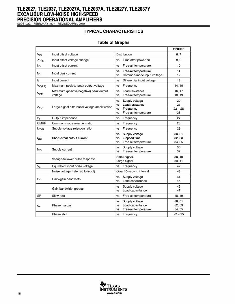
Table of Graphs
FIGURE
VIO Input offset voltage Distribution 6, 7
ΔVIO Input offset voltage change vs Time after power on 8, 9
IIO Input offset current vs Free-air temperature 10
I Input bias currentvs Free-air temperature 11
IIB Input bias currentvsvs
Free air temperatureCommon-mode input voltage
1112
II Input current vs Differential input voltage 13
VO(PP) Maximum peak-to-peak output voltage vs Frequency 14, 15
VMaximum (positive/negative) peak output vs Load resistance 16, 17
VOMMaximum (positive/negative) peak outputvoltage
vsvs
Load resistanceFree-air temperature
16, 1718, 19
vs Supply voltage 20
A Large signal differential voltage amplification
vsvs
Supply voltageLoad resistance
2021
AVD Large-signal differential voltage amplificationvsvs
Load resistanceFrequency
2122 − 25vs
vsFrequencyFree-air temperature
22 2526
zo Output impedance vs Frequency 27
CMRR Common-mode rejection ratio vs Frequency 28
kSVR Supply-voltage rejection ratio vs Frequency 29
vs Supply voltage 30, 31IOS Short-circut output current
vsvs
Supply voltageElapsed time
30, 3132, 33IOS Short circut output current vs
vsElapsed timeFree-air temperature
32, 3334, 35
I Supply currentvs Supply voltage 36
ICC Supply currentvsvs
Supply voltageFree-air temperature
3637
Voltage follower pulse responseSmall signal 38, 40
Voltage-follower pulse responseSmall signalLarge signal
38, 4039, 41
Vn Equivalent input noise voltage vs Frequency 42
Noise voltage (referred to input) Over 10-second interval 43
B Unity gain bandwidthvs Supply voltage 44
B1 Unity-gain bandwidthvsvs
Supply voltageLoad capacitance
4445
Gain bandwidth productvs Supply voltage 46
Gain bandwidth productvsvs
Supply voltageLoad capacitance
4647
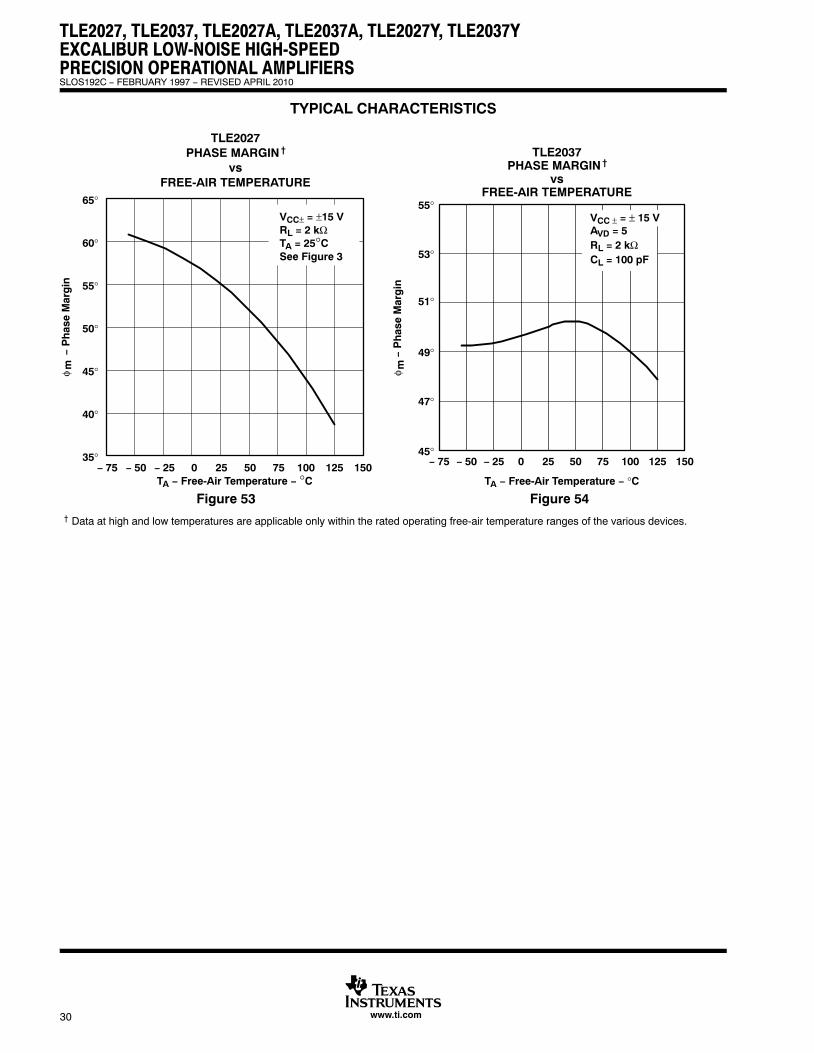
SR Slew rate vs Free-air temperature 48, 49
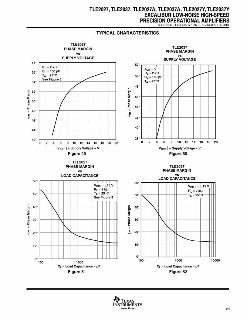
vs Supply voltage 50, 51φm Phase margin
vsvs
Supply voltageLoad capacitance
50, 5152, 53φm Phase margin vs
vsLoad capacitanceFree-air temperature
52, 5354, 55
Phase shift vs Frequency 22 − 25

TLE2027, TLE2037, TLE2027A, TLE2037A, TLE2027Y, TLE2037YEXCALIBUR LOW-NOISE HIGH-SPEED
PRECISION OPERATIONAL AMPLIFIERS
�
SLOS192C − FEBRUARY 1997 − REVISED APRIL 2010
17www.ti.com
TYPICAL CHARACTERISTICS
Figure 6
Per
cen
tag
e o
f Am
plif
iers
− %
VIO − Input Offset Voltage − μV
TA = 25°CVCC± = +15 V
16
14
12
10
8
6
4
2
0 120906030− 30− 60− 90− 1200
ÎÎÎÎD Package
ÎÎÎÎÎÎÎÎÎÎÎÎ1568 Amplifiers Tested From 2 Wafer Lots
DISTRIBUTIONINPUT OFFSET VOLTAGE
Figure 7
INPUT OFFSET VOLTAGE CHANGEvs
TIME AFTER POWER ON
00
t − Time After Power On − s10 20 30 40 50 60
2
4
6
8
10
12
ÁÁÁÁÁÁÁÁÁÁÁÁÁÁÁÁÁÁA
VIO
− C
han
ge
in In
pu
t O
ffse
t Vo
ltag
e −
ÁÁÁÁÁÁ
ΔV I
Oμ
V
ÎÎÎÎÎÎÎÎÎÎÎÎÎÎÎÎÎÎÎÎÎÎ
50 Amplifiers Tested From 2 Wafer LotsVCC± = ±15 VTA = 25°C
ÎÎÎÎÎÎÎÎ
D Package
Figure 8t − Time After Power On − s
INPUT OFFSET VOLTAGE CHANGEvs
TIME AFTER POWER ON6
5
4
3
2
1
00 20 40 60 80 100 120 140 160 180
AV
IO −
Ch
ang
e in
Inp
ut
Off
set
Volt
age −
ÁÁÁÁ
ΔV
IOμ
V
ÎÎÎÎÎÎÎÎÎÎÎÎÎÎÎÎÎÎÎÎÎÎ
50 Amplifiers Tested From 2 Wafer LotsVCC± = ±15 VTA = 25°CÎÎÎÎÎÎÎÎ
P Package
Figure 9
0
IIO −
Inp
ut
Off
set
Cu
rren
t −
nA
5
10
15
20
25
30
1501251007550250− 25− 50
TA − Free-Air Temperature − °C
− 75
INPUT OFFSET CURRENT†
vsFREE-AIR TEMPERATURE
IOI
ÁÁÁÁÁÁÁÁÁÁÁÁÁÁÁÁÁÁÁÁÁÁÁÁÁÁÁÁ
VCC± = ±15 VVIC = 0Sample Size = 833 UnitsFrom 2 Wafer Lots
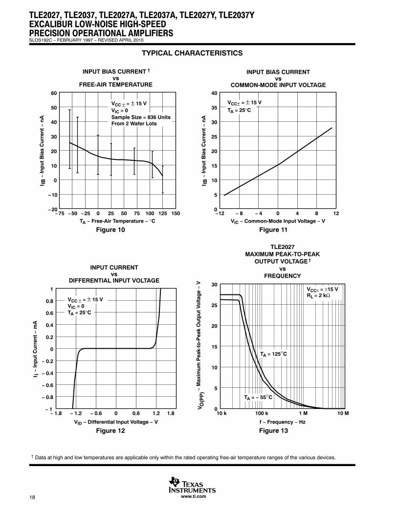
† Data at high and low temperatures are applicable only within the rated operating free-air temperature ranges of the various devices.
TLE2027, TLE2037, TLE2027A, TLE2037A, TLE2027Y, TLE2037YEXCALIBUR LOW-NOISE HIGH-SPEEDPRECISION OPERATIONAL AMPLIFIERS
�
SLOS192C − FEBRUARY 1997 − REVISED APRIL 2010
18 www.ti.com
TYPICAL CHARACTERISTICS
Figure 10
INPUT BIAS CURRENT †
vsFREE-AIR TEMPERATURE
−20−75
IIB −
Inp
ut
Bia
s C
urr
ent −
nA
TA − Free-Air Temperature − °C
−10
0
10
20
30
40
50
60
−50 −25 0 25 50 75 100 125 150
ÁÁÁÁÁÁÁÁÁÁÁÁÁÁÁÁÁÁÁÁÁÁÁÁÁÁÁÁÁÁÁÁ
VCC ± = ± 15 VVIC = 0Sample Size = 836 UnitsFrom 2 Wafer Lots
IBI
Figure 11
INPUT BIAS CURRENTvs
COMMON-MODE INPUT VOLTAGE
0−12
VIC − Common-Mode Input Voltage − V− 8 − 4 0 4 8 12
5
10
15
20
25
30
35
40
TA = 25°CVCC± = ± 15 V
IIB −
Inp
ut
Bia
s C
urr
ent −
nA
IBI
Figure 12
II −
Inp
ut
Cu
rren
t −
mA
− 1− 1.8
VID − Differential Input Voltage − V
− 0.8
− 0.6
− 0.4
− 0.2
0
0.2
0.4
0.6
0.8
1
− 1.2 − 0.6 0 0.6 1.2 1.8
INPUT CURRENTvs
DIFFERENTIAL INPUT VOLTAGE
II
ÁÁÁÁÁÁÁÁÁÁÁÁÁÁÁ
VCC ± = ± 15 VVIC = 0TA = 25°C
Figure 13
V O(P
P)−
Max
imu
m P
eak-
to-P
eak
Ou
tpu
t Vo
ltag
e −
V
TA = − 55°C
TA = 125°C
10 M1 M100 k
30
25
20
15
10
5
f − Frequency − Hz
10 k0
ÎÎÎÎÎÎÎÎÎÎÎÎÎÎÎ
VCC± = ±15 VRL = 2 kΩ
TLE2027MAXIMUM PEAK-TO-PEAK
OUTPUT VOLTAGE†
vsFREQUENCY
† Data at high and low temperatures are applicable only within the rated operating free-air temperature ranges of the various devices.
TLE2027, TLE2037, TLE2027A, TLE2037A, TLE2027Y, TLE2037YEXCALIBUR LOW-NOISE HIGH-SPEED
PRECISION OPERATIONAL AMPLIFIERS
�
SLOS192C − FEBRUARY 1997 − REVISED APRIL 2010
19www.ti.com
TYPICAL CHARACTERISTICS
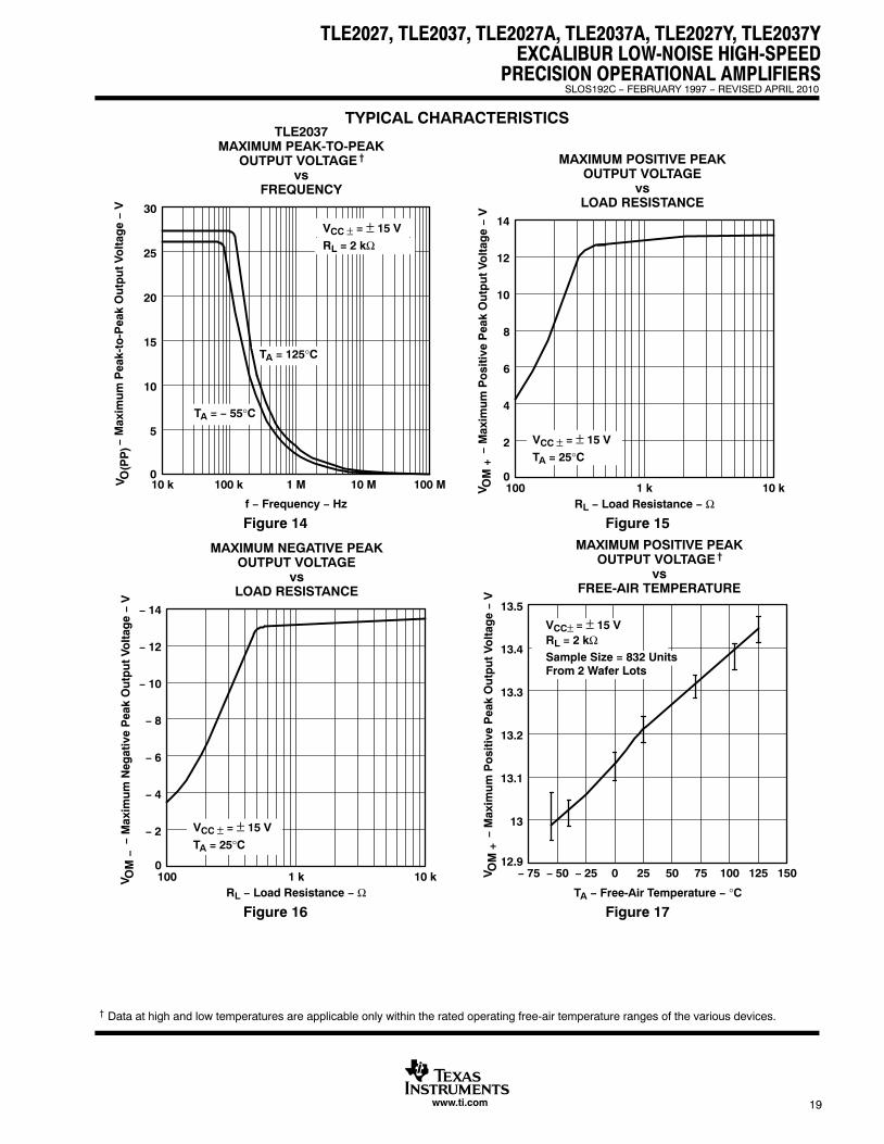
Figure 14
VO
(PP
) −
Max
imu
m P
eak-
to-P
eak
Ou
tpu
t Vo
ltag
e −
V
010 k
f − Frequency − Hz
5
10
15
20
25
30
100 k 1 M 100 M
TA = − 55°C
10 M
ÁÁÁÁÁÁÁÁÁ
V O(P
P)
ÁÁÁÁÁÁÁÁÁÁÁÁÁÁÁÎÎÎÎÎÎÎÎÎÎ
RL = 2 kΩ
ÎÎÎÎÎÎÎÎÎÎVCC ± = ± 15 V
ÎÎÎÎÎÎÎÎ
TA = 125°C
TLE2037MAXIMUM PEAK-TO-PEAK
OUTPUT VOLTAGE†
vsFREQUENCY
Figure 15
MAXIMUM POSITIVE PEAKOUTPUT VOLTAGE
vsLOAD RESISTANCE
0100V
OM
+ −
Max
imu
m P
osi
tive
Pea
k O
utp
ut
Volt
age −
V
RL − Load Resistance − Ω
2
4
6
8
10
12
14
1 k 10 k
ÁÁÁÁÁÁ
V OM
+
ÁÁÁÁÁÁÁÁÁÁÁÁÁÁÁÁÁÁ
VCC ± = ± 15 V
TA = 25°C
Figure 16
0100V
OM− −
Max
imu
m N
egat
ive
Pea
k O
utp
ut
Volt
age −
V
RL − Load Resistance − Ω
− 2
− 4
− 6
− 8
− 10
− 12
− 14
1 k 10 k
MAXIMUM NEGATIVE PEAKOUTPUT VOLTAGE
vsLOAD RESISTANCE
ÁÁÁÁÁÁ
V OM−
ÁÁÁÁÁÁÁÁÁÁÁÁÁÁÁ
VCC ± = ± 15 V
TA = 25°C
Figure 17
MAXIMUM POSITIVE PEAKOUTPUT VOLTAGE†
vsFREE-AIR TEMPERATURE
12.9− 75
TA − Free-Air Temperature − °C
13
13.1
13.2
13.3
13.4
13.5
− 50 − 25 0 25 50 75 100 125 150VO
M+ −
Max
imu
m P
osi
tive
Pea
k O
utp
ut
Volt
age −
V
ÁÁÁÁÁÁV
OM
+
ÎÎÎÎÎÎÎÎÎÎ
VCC± = ± 15 VÎÎÎÎÎÎÎÎÎÎ
RL = 2 kΩ
ÎÎÎÎÎÎÎÎÎÎÎÎ
From 2 Wafer LotsÎÎÎÎÎÎÎÎÎÎÎÎÎÎ
Sample Size = 832 Units
† Data at high and low temperatures are applicable only within the rated operating free-air temperature ranges of the various devices.
TLE2027, TLE2037, TLE2027A, TLE2037A, TLE2027Y, TLE2037YEXCALIBUR LOW-NOISE HIGH-SPEEDPRECISION OPERATIONAL AMPLIFIERS
�
SLOS192C − FEBRUARY 1997 − REVISED APRIL 2010
20 www.ti.com
TYPICAL CHARACTERISTICS
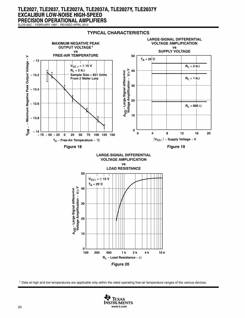
Figure 18
MAXIMUM NEGATIVE PEAKOUTPUT VOLTAGE†
vsFREE-AIR TEMPERATURE
− 14− 75
TA − Free-Air Temperature − °C
− 13.8
− 13.6
− 13.4
− 13.2
− 13
− 50 − 25 0 25 50 75 100 125 150
ÎÎÎÎÎRL = 2 kΩÎÎÎÎÎÎÎÎÎÎ
VCC ± = ± 15 V
VO
M− −
Max
imu
m N
egat
ive
Pea
k O
utp
ut
Volt
age −
V
ÁÁÁÁÁÁÁÁÁ
V OM−
ÎÎÎÎÎÎÎÎÎÎÎÎÎÎÎÎ
Sample Size = 831 UnitsÎÎÎÎÎÎÎÎÎÎÎÎ
From 2 Wafer Lots
Figure 19
LARGE-SIGNAL DIFFERENTIALVOLTAGE AMPLIFICATION
vsSUPPLY VOLTAGE
00
⎟ VCC±⎟ − Supply Voltage − V
50
4 8 12 16 20
10
20
30
40RL = 2 kΩ
RL = 1 kΩ
RL = 600 Ω
ÎÎÎÎTA = 25°C
AV
D −
Lar
ge-
Sig
nal
dif
fere
nti
al
ÁÁÁÁÁÁ
AV
DV
μV
/V
olt
age
Am
plif
icat
ion
−
Figure 20
10
0
50
100 200 400 1 k 4 k 10 k2 k
40
30
20
RL − Load Resistance − Ω
ÁÁÁÁÁÁÁÁÁÁÁÁ
TA = 25°CVCC± = ± 15 V
AV
D −
Lar
ge-
Sig
nal
dif
fere
nti
al
ÁÁÁÁÁÁ
AV
DV
μV
/V
olt
age
Am
plif
icat
ion
−
LARGE-SIGNAL DIFFERENTIALVOLTAGE AMPLIFICATION
vsLOAD RESISTANCE
† Data at high and low temperatures are applicable only within the rated operating free-air temperature ranges of the various devices.
TLE2027, TLE2037, TLE2027A, TLE2037A, TLE2027Y, TLE2037YEXCALIBUR LOW-NOISE HIGH-SPEED
PRECISION OPERATIONAL AMPLIFIERS
�
SLOS192C − FEBRUARY 1997 − REVISED APRIL 2010
21www.ti.com
TYPICAL CHARACTERISTICS
AVD
Phase Shift
VCC± = ± 15 VRL = 2 kΩCL = 100 pFTA = 25°C
Ph
ase
Sh
ift
275°
75°
250°
225°
200°
175°
150°
125°
100°140
120
100
80
60
40
20
100 k100
160
100 Mf − Frequency − Hz
00.1
AV
D −
Lar
ge-
Sig
nal
Dif
fere
nti
al
ÁÁÁÁ
AV
D Vo
ltag
e A
mp
lific
atio
n −
dB
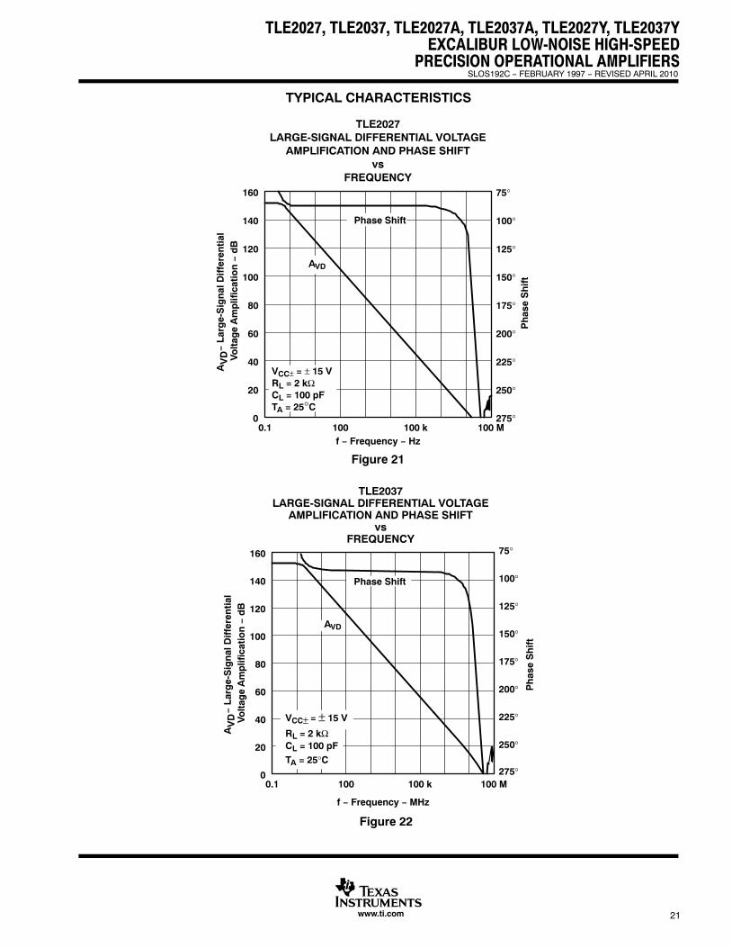
Figure 21
TLE2027LARGE-SIGNAL DIFFERENTIAL VOLTAGE
AMPLIFICATION AND PHASE SHIFTvs
FREQUENCY
0.10
f − Frequency − MHz
100 M
160
100 100 k
20
40
60
80
100
120
140 100°
125°
150°
175°
200°
225°
250°
75°
275°
ÎÎÎÎÎÎÎÎÎÎ
Phase Shift
ÎÎÎÎ
AVD
Ph
ase
Sh
ift
AV
D −
Lar
ge-
Sig
nal
Dif
fere
nti
al
ÁÁÁ
AV
D Vo
ltag
e A
mp
lific
atio
n −
dB
ÁÁÁÁÁÁÁÁÁÁÁÁÁÁÁÁÁÁÁÁTA = 25°C
CL = 100 pF
VCC± = ± 15 V
RL = 2 kΩ
Figure 22
TLE2037LARGE-SIGNAL DIFFERENTIAL VOLTAGE
AMPLIFICATION AND PHASE SHIFTvs
FREQUENCY
TLE2027, TLE2037, TLE2027A, TLE2037A, TLE2027Y, TLE2037YEXCALIBUR LOW-NOISE HIGH-SPEEDPRECISION OPERATIONAL AMPLIFIERS
�
SLOS192C − FEBRUARY 1997 − REVISED APRIL 2010
22 www.ti.com
TYPICAL CHARACTERISTICS
300°
100°
275°
250°
225°
200°
175°
150°
125°
Ph
ase
Sh
ift
AVD
Phase Shift
704020
3
0
− 3
− 6
− 9
− 12
− 15
6
100
f − Frequency − MHz
− 1810
ÎÎÎÎÎÎÎÎÎÎÎÎÎÎÎ
VCC± = ± 15 VRL = 2 kΩCL = 100 pFTA = 25°C
AV
D −
Lar
ge-
Sig
nal
Dif
fere
nti
al
ÁÁÁÁÁÁ
AV
D Vo
ltag
e A
mp
lific
atio
n −
dB
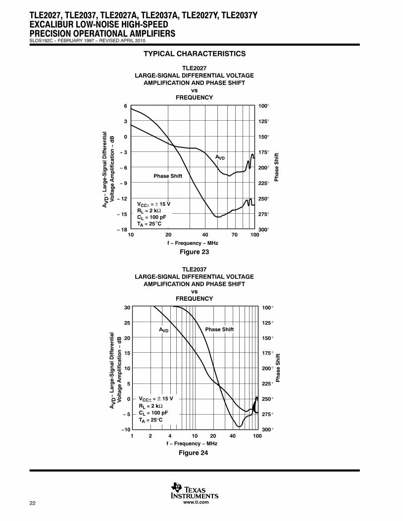
Figure 23
TLE2027LARGE-SIGNAL DIFFERENTIAL VOLTAGE
AMPLIFICATION AND PHASE SHIFTvs
FREQUENCY
− 5
−10
15
1 2 4 10 40 10020
10
5
0
30
25
20
f − Frequency − MHz
Ph
ase
Sh
ift
275
300
175
200
225
250
100
125
150
°
°
°
°
°
°
°
°
°
ÎÎÎÎÎPhase ShiftÎÎÎAVD
AV
D −
Lar
ge-
Sig
nal
Dif
fere
nti
al
ÁÁÁÁ
AV
D Vo
ltag
e A
mp
lific
atio
n −
dB
ÁÁÁÁÁÁÁÁÁÁÁÁÁÁÁÁÁÁÁÁ
TA = 25°CCL = 100 pFRL = 2 kΩVCC± = ± 15 V
Figure 24
TLE2037LARGE-SIGNAL DIFFERENTIAL VOLTAGE
AMPLIFICATION AND PHASE SHIFTvs
FREQUENCY
TLE2027, TLE2037, TLE2027A, TLE2037A, TLE2027Y, TLE2037YEXCALIBUR LOW-NOISE HIGH-SPEED
PRECISION OPERATIONAL AMPLIFIERS
�
SLOS192C − FEBRUARY 1997 − REVISED APRIL 2010
23www.ti.com
TYPICAL CHARACTERISTICS
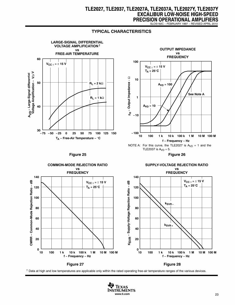
Figure 25
−7530
TA − Free-Air Temperature − °C150
60
−50 −25 0 25 50 75 100 125
40
50
VCC ± = ± 15 V
ÎÎÎÎÎÎÎÎÎÎ
RL = 2 kΩ
ÎÎÎÎÎRL = 1 kΩ
LARGE-SIGNAL DIFFERENTIALVOLTAGE AMPLIFICATION†
vsFREE-AIR TEMPERATURE
AV
D −
Lar
ge-
Sig
nal
dif
fere
nti
al
ÁÁÁÁÁÁ
AV
DV
μV
/V
olt
age
Am
plif
icat
ion
−
OUTPUT IMPEDANCEvs
FREQUENCY
Figure 26
10−100
zo −
Ou
tpu
t Im
ped
ance
−
f − Frequency − Hz
100 M
100
100 1 k 10 k 100 k 1 M 10 M
−10
1
10
AVD = 100
See Note A
AVD = 10
ÁÁÁÁz
o
ÁÁÁÁ
Ω
ÁÁÁÁÁÁÁÁÁÁ
VCC ± = ± 15 VTA = 25°C
NOTE A: For this curve, the TLE2027 is AVD = 1 and theTLE2037 is AVD = 5.
100
CM
RR
− C
om
mo
n-M
od
e R
ejec
tio
n R
atio
− d
B
f − Frequency − Hz100 M
140
100 1 k 10 k 100 k 1 M 10 M
20
40
60
80
100
120
COMMON-MODE REJECTION RATIOvs
FREQUENCY
ÁÁÁÁÁÁÁÁÁÁÁÁÎÎÎÎTA = 25°CÎÎÎÎÎÎÎÎÎÎ
VCC ± = ± 15 V
Figure 27
100
− S
up
ply
-Vo
ltag
e R
ejec
tio
n R
atio
− d
B
f − Frequency − Hz100 M
140
100 1 k 10 k 100 k 1 M 10 M
20
40
60
80
100
120
ÎÎÎÎkSVR−
ÎÎÎÎÎÎ
kSVR +
SUPPLY-VOLTAGE REJECTION RATIOvs
FREQUENCY
ÁÁÁÁÁÁÁÁÎÎÎÎTA = 25°CÎÎÎÎÎÎVCC ± = ± 15 V
SV
RK
Figure 28† Data at high and low temperatures are applicable only within the rated operating free-air temperature ranges of the various devices.
TLE2027, TLE2037, TLE2027A, TLE2037A, TLE2027Y, TLE2037YEXCALIBUR LOW-NOISE HIGH-SPEEDPRECISION OPERATIONAL AMPLIFIERS
�
SLOS192C − FEBRUARY 1997 − REVISED APRIL 2010
24 www.ti.com
TYPICAL CHARACTERISTICS
0−30
IOS
− S
ho
rt-C
ircu
it O
utp
ut
Cu
rren
t −
mA
−42
2 4 6 8 10 12 14 16 18 20
−32
−34
−36
−38
−40
SHORT-CIRCUIT OUTPUT CURRENTvs
SUPPLY VOLTAGE
⎟ VCC±⎟ − Supply Voltage − V
ÁÁÁÁÁÁÁÁÁÁÁÁÁÁÁÁÁÁÁÁ
VID = 100 mVVO = 0TA = 25°C
ÎÎÎÎP Package
ÁÁÁÁ
OS
I
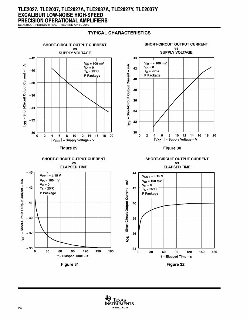
Figure 29
SHORT-CIRCUIT OUTPUT CURRENTvs
SUPPLY VOLTAGE
030
44
2 4 6 8 10 12 14 16 18 20
32
34
36
38
40
42
ÁÁÁÁÁÁÁÁÁÁÁÁÁÁÁÁÁÁÁÁÁÁÁÁ
VID = − 100 mVVO = 0TA = 25°CP Package
IOS
− S
ho
rt-C
ircu
it O
utp
ut
Cu
rren
t −
mA
ÁÁÁÁ
OS
I
⎟ VCC±⎟ − Supply Voltage − V
Figure 30
0− 35
t − Elasped Time − s180
− 45
30 60 90 120 150
− 37
− 39
− 41
− 43
SHORT-CIRCUIT OUTPUT CURRENTvs
ELAPSED TIME
ÁÁÁÁÁÁÁÁÁÁÁÁÁÁÁÁÁÁÁÁÎÎÎÎ
P PackageTA = 25°CVO = 0VID = 100 mV
VCC ± = ± 15 V
IOS
− S
ho
rt-C
ircu
it O
utp
ut
Cu
rren
t −
mA
ÁÁÁÁÁÁÁÁÁ
OS
I
Figure 31
SHORT-CIRCUIT OUTPUT CURRENTvs
ELAPSED TIME
034
t − Elasped Time − s180
44
30 60 90 120 150
36
38
40
42
IOS
− S
ho
rt-C
ircu
it O
utp
ut
Cu
rren
t −
mA
ÁÁÁÁ
OS
I
ÁÁÁÁÁÁÁÁÁÁÁÁÁÁÁÁÁÁÁÁÁÁÁÁÁÎÎÎÎÎ
P PackageTA = 25°CVO = 0VID = 100 mV
VCC ± = ± 15 V
Figure 32
TLE2027, TLE2037, TLE2027A, TLE2037A, TLE2027Y, TLE2037YEXCALIBUR LOW-NOISE HIGH-SPEED
PRECISION OPERATIONAL AMPLIFIERS
�
SLOS192C − FEBRUARY 1997 − REVISED APRIL 2010
25www.ti.com
TYPICAL CHARACTERISTICS
− 75− 24
TA − Free-Air Temperature − °C150
− 48
− 50 − 25 0 25 50 75 100 125
− 28
− 32
− 36
− 40
− 44
SHORT-CIRCUIT OUTPUT CURRENT †
vsFREE-AIR TEMPERATURE
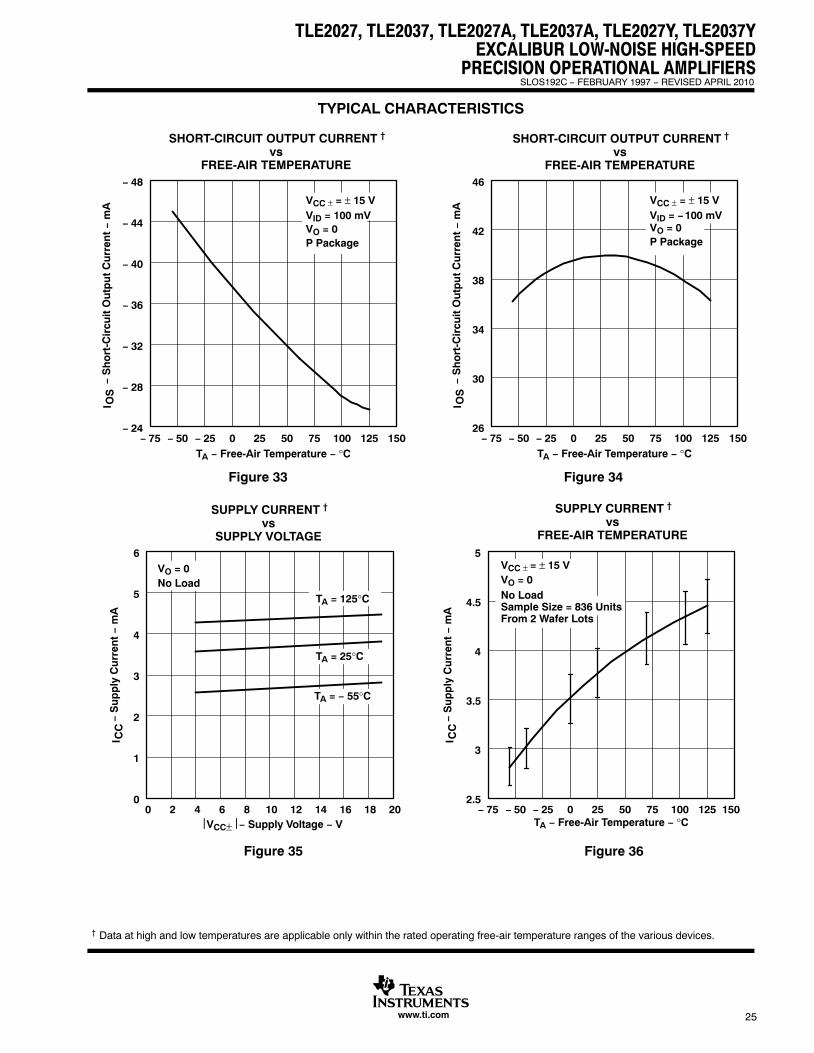
IOS
− S
ho
rt-C
ircu
it O
utp
ut
Cu
rren
t −
mA
ÁÁÁÁÁÁ
OS
I
ÁÁÁÁÁÁÁÁÁÁÁÁÁÁÁÁÁÁÁÁ
VCC ± = ± 15 VVID = 100 mVVO = 0P Package
Figure 33
26
TA − Free-Air Temperature − °C
46
30
34
38
42
1251007550250− 25− 50 150− 75
SHORT-CIRCUIT OUTPUT CURRENT †
vsFREE-AIR TEMPERATURE
IOS
− S
ho
rt-C
ircu
it O
utp
ut
Cu
rren
t −
mA
ÁÁÁÁÁÁ
OS
I
ÁÁÁÁÁÁÁÁÁÁÁÁÁÁÁÁÁÁÁÁ
VCC ± = ± 15 VVID = −100 mVVO = 0P Package
Figure 34
ÁÁÁÁÁÁÁÁ
00
ICC
− S
up
ply
Cu
rren
t −
mA
⎟ VCC±⎟ − Supply Voltage − V
6
2 4 6 8 10 12 14 16 18 20
1
2
3
4
5
SUPPLY CURRENT †
vsSUPPLY VOLTAGE
ÁÁÁÁ
CC
I
VO = 0No Load
ÎÎÎÎTA = 125°C
ÎÎÎÎÎÎÎÎ
TA = 25°C
ÎÎÎÎÎÎÎÎ
TA = − 55°C
Figure 35
− 752.5
TA − Free-Air Temperature − °C150
5
− 50 − 25 0 25 50 75 100 125
3
3.5
4
4.5
SUPPLY CURRENT †
vsFREE-AIR TEMPERATURE
ICC
− S
up
ply
Cu
rren
t −
mA
ÁÁÁÁ
CC
I
ÁÁÁÁÁÁÁÁÁÁÁÁÁÁÁÁÁÁÁÁÁÁÁÁÁÁÁÁ
VCC ± = ± 15 VVO = 0No LoadSample Size = 836 UnitsFrom 2 Wafer Lots
Figure 36
† Data at high and low temperatures are applicable only within the rated operating free-air temperature ranges of the various devices.

TLE2027, TLE2037, TLE2027A, TLE2037A, TLE2027Y, TLE2037YEXCALIBUR LOW-NOISE HIGH-SPEEDPRECISION OPERATIONAL AMPLIFIERS
�
SLOS192C − FEBRUARY 1997 − REVISED APRIL 2010
26 www.ti.com
TYPICAL CHARACTERISTICS
Figure 37
VO
− O
utp
ut
Volt
age −
mV 50
0
− 50
8006004002000
100
1000t − Time − ns
− 100
ÎÎÎÎÎÎÎÎÎÎÎÎÎÎÎÎÎÎÎÎ
VCC± = ±15 VRL = 2 kΩCL = 100 pFTA = 25°CSee Figure 4
TLE2027VOLTAGE-FOLLOWER
SMALL-SIGNALPULSE RESPONSE
Figure 38
t − Time − μs250 5 10 15 20
10
5
0
− 5
− 10
15
− 15
ÎÎÎÎÎÎÎÎÎÎÎÎÎÎÎÎÎÎÎÎ
VCC± = ±15 VRL = 2 kΩCL = 100 pFTA = 25°CSee Figure 1
V O−
Ou
tpu
t Vo
ltag
e −
V
TLE2027VOLTAGE-FOLLOWER
LARGE-SIGNALPULSE RESPONSE
ÁÁÁÁÁÁÁÁÁÁÁÁÁÁÁÁÁÁÁÁÁÁÁÁ
TA = 25°CSee Figure 4
VCC ± = ± 15 VAVD = 5RL = 2 kΩCL = 100 pF
50
0
− 50
3002001000
100
400
t − Time − ns
− 100
VO
− O
utp
ut
Volt
age −
mV
ÁÁÁÁ
VO
Figure 39
TLE2037VOLTAGE-FOLLOWER
SMALL-SIGNALPULSE RESPONSE
− 15
15
− 10
− 5
0
5
10
TA = 25°CCL = 100 pFRL = 2 kΩAVD = 5ÎÎÎÎÎÎÎÎÎÎÎÎ
VCC ± = ± 15 V
86420 10t − Time − μs
VO
− O
utp
ut
Volt
age −
V
ÁÁÁÁ
V O
ÎÎÎÎÎÎÎÎÎÎ
See Figure 1
Figure 40
TLE2037VOLTAGE-FOLLOWER
LARGE-SIGNALPULSE RESPONSE
TLE2027, TLE2037, TLE2027A, TLE2037A, TLE2027Y, TLE2037YEXCALIBUR LOW-NOISE HIGH-SPEED
PRECISION OPERATIONAL AMPLIFIERS
�
SLOS192C − FEBRUARY 1997 − REVISED APRIL 2010
27www.ti.com
TYPICAL CHARACTERISTICS
10
Vn
− E
qu
ival
ent
Inp
ut
No
ise
Volt
age −
nV
Hz
f − Frequency − Hz
100 k
10
10 100 1 k 10 k
2
4
6
8
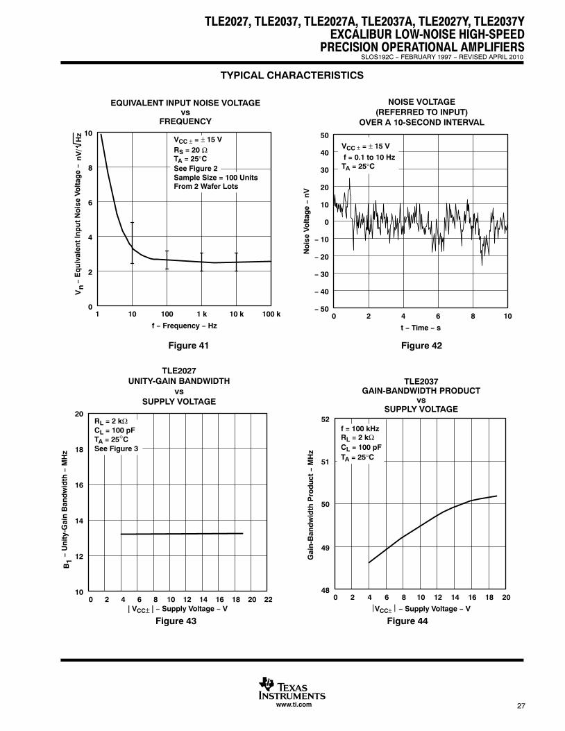
EQUIVALENT INPUT NOISE VOLTAGEvs
FREQUENCY
ÁÁÁÁÁÁÁÁÁÁÁÁÁÁÁÁÁÁÁÁÁÁÁÁÁÁÁÁÁÁÁÁÁÁÁ
VCC ± = ± 15 VRS = 20 ΩTA = 25°CSee Figure 2Sample Size = 100 UnitsFrom 2 Wafer Lots
Vn
ÁÁÁÁÁÁ
nV
/H
z
Figure 41
NOISE VOLTAGE(REFERRED TO INPUT)
OVER A 10-SECOND INTERVAL
0− 50
No
ise
Volt
age −
nV
t − Time − s
10
50
2 4 6 8
− 40
− 30
− 20
− 10
0
10
20
30
40
ÁÁÁÁÁÁÁÁÁÁÁÁÁÁÁÁÁÁÁÁÁÁÁÁ
VCC ± = ± 15 V
f = 0.1 to 10 HzTA = 25°C
Figure 42
Figure 43
20
B1−
Un
ity-
Gai
n B
and
wid
th −
MH
z 18
16
14
12
2018161412108642 22| VCC± | − Supply Voltage − V
100
RL = 2 kΩCL = 100 pFTA = 25°CSee Figure 3
TLE2027UNITY-GAIN BANDWIDTH
vsSUPPLY VOLTAGE
Figure 44
048
⎟ VCC±⎟ − Supply Voltage − V
52
2 4 6 8 10 12 14 16 18 20
49
50
51
ÁÁÁÁÁÁÁÁÁÁÁÁÁÁÁÁÁÁÁÁ
RL = 2 kΩCL = 100 pFTA = 25°C
f = 100 kHz
Gai
n-B
and
wid
th P
rod
uct
− M
Hz
TLE2037GAIN-BANDWIDTH PRODUCT
vsSUPPLY VOLTAGE
TLE2027, TLE2037, TLE2027A, TLE2037A, TLE2027Y, TLE2037YEXCALIBUR LOW-NOISE HIGH-SPEEDPRECISION OPERATIONAL AMPLIFIERS
�
SLOS192C − FEBRUARY 1997 − REVISED APRIL 2010
28 www.ti.com
TYPICAL CHARACTERISTICS
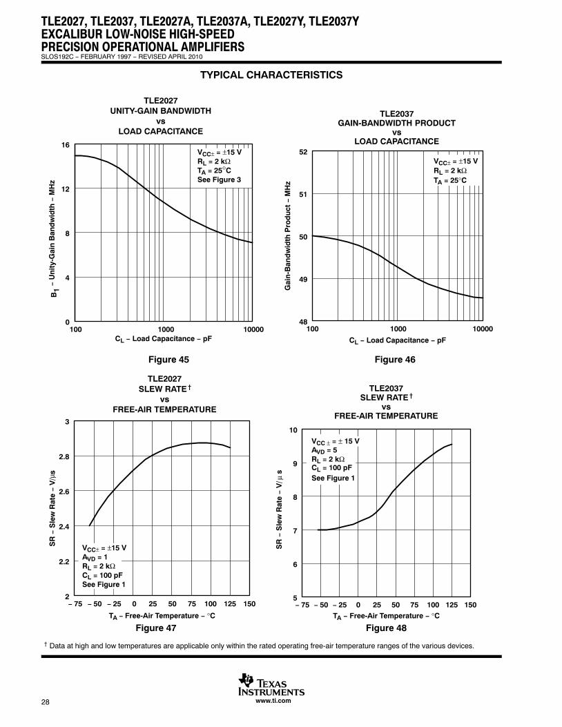
Figure 45
VCC± = ±15 VRL = 2 kΩTA = 25°CSee Figure 3
1000
12
8
4
16
10000CL − Load Capacitance − pF
0100
B1−
Un
ity-
Gai
n B
and
wid
th −
MH
z
TLE2027UNITY-GAIN BANDWIDTH
vsLOAD CAPACITANCE
10048
Gai
n-B
and
wid
th P
rod
uct
− M
Hz
CL − Load Capacitance − pF
10000
52
49
50
51
1000
ÁÁÁÁÁÁÁÁÁÁÁÁÁÁÁÁÁÁ
TA = 25°CRL = 2 kΩVCC± = ±15 V
Figure 46
TLE2037GAIN-BANDWIDTH PRODUCT
vsLOAD CAPACITANCE
Figure 47
ÎÎÎÎÎÎÎÎÎÎÎÎÎÎÎÎÎÎÎÎ
VCC± = ±15 VAVD = 1RL = 2 kΩCL = 100 pFSee Figure 1
2.8
2.6
2.4
2.2
1251007550250− 25− 50
3
150
TA − Free-Air Temperature − °C
SR
− S
lew
Rat
e −
V/
s
2− 75
μ
TLE2027SLEW RATE†
vsFREE-AIR TEMPERATURE
Figure 48
− 755
TA − Free-Air Temperature − °C150
10
− 50 − 25 0 25 50 75 100 125
6
7
8
9
sμ
ÁÁÁÁÁÁÁÁÁÁÁÁÁÁÁÁÁÁÁÁÁÁÁÁÁ
AVD = 5RL = 2 kΩCL = 100 pFSee Figure 1
SR
− S
lew
Rat
e −
V/
ÎÎÎÎÎÎÎÎÎÎÎÎ
VCC ± = ± 15 V
TLE2037SLEW RATE†
vsFREE-AIR TEMPERATURE
† Data at high and low temperatures are applicable only within the rated operating free-air temperature ranges of the various devices.
TLE2027, TLE2037, TLE2027A, TLE2037A, TLE2027Y, TLE2037YEXCALIBUR LOW-NOISE HIGH-SPEED
PRECISION OPERATIONAL AMPLIFIERS
�
SLOS192C − FEBRUARY 1997 − REVISED APRIL 2010
29www.ti.com
TYPICAL CHARACTERISTICS
Figure 49
56°
54°
52°
50°
48°
46°
44°
2018161412108642
58°
22
| VCC± | − Supply Voltage − V
− P
has
e M
arg
in
42°0
ÎÎÎÎÎÎÎÎÎÎÎÎÎÎÎÎÎÎÎÎ
RL = 2 kΩCL = 100 pFTA = 25°CSee Figure 3
ÁÁÁÁ
mφ
TLE2027PHASE MARGIN
vsSUPPLY VOLTAGE
Figure 50
0
m
⎟ VCC±⎟ − Supply Voltage − V
2 4 6 8 10 12 14 16 18 2038°
40°
42°
44°
46°
48°
50°
52°
φ
ÁÁÁÁÁÁÁÁÁÁÁÁÁÁÁÁÁÁÁÁ
TA = 25°CCL = 100 pF
AVD = 5RL = 2 kΩ
− P
has
e M
arg
in
TLE2037PHASE MARGIN
vsSUPPLY VOLTAGE
Figure 51
1000
40°
20°
60°
CL − Load Capacitance − pF
0°100
− P
has
e M
arg
in
ÁÁÁÁ
mφ
TLE2027PHASE MARGIN
vsLOAD CAPACITANCE
ÎÎÎÎÎÎÎÎÎÎÎÎÎÎÎÎÎÎÎÎ
VCC± = ±15 VRL = 2 kΩTA = 25°CSee Figure 3
10°
30°
50°
Figure 52
1000°
CL − Load Capacitance − pF
100001000
10°
20°
30°
40°
50°
60° ÁÁÁÁÁÁÁÁÁÁÁÁÁÁÁ
VCC ± = ± 15 VRL = 2 kΩTA = 25°C
mφ −
Ph
ase
Mar
gin
TLE2037PHASE MARGIN
vsLOAD CAPACITANCE
† Data at high and low temperatures are applicable only within the rated operating free-air temperature ranges of the various devices.
TLE2027, TLE2037, TLE2027A, TLE2037A, TLE2027Y, TLE2037YEXCALIBUR LOW-NOISE HIGH-SPEEDPRECISION OPERATIONAL AMPLIFIERS
�
SLOS192C − FEBRUARY 1997 − REVISED APRIL 2010
30 www.ti.com
TYPICAL CHARACTERISTICS
Figure 53
− P
has
e M
arg
in
ÁÁÁÁ
mφ
60°
55°
50°
45°
40°
1251007550250− 25− 50
65°
150TA − Free-Air Temperature − °C
35°− 75
ÎÎÎÎÎÎÎÎÎÎÎÎÎÎÎ
VCC± = ±15 VRL = 2 kΩTA = 25°CSee Figure 3
TLE2027PHASE MARGIN†
vsFREE-AIR TEMPERATURE
Figure 54
− 7545°
TA − Free-Air Temperature − °C
150− 50 − 25 0 25 50 75 100 125
49°
51°
53°
55°
47°
ÁÁÁÁÁÁÁÁÁÁÁÁÁÁÁÁÁÁÁÁÁÁÁÁ
CL = 100 pFRL = 2 kΩAVD = 5VCC ± = ± 15 V
mφ −
Ph
ase
Mar
gin
TLE2037PHASE MARGIN†
vsFREE-AIR TEMPERATURE
TLE2027, TLE2037, TLE2027A, TLE2037A, TLE2027Y, TLE2037YEXCALIBUR LOW-NOISE HIGH-SPEED
PRECISION OPERATIONAL AMPLIFIERS
�
SLOS192C − FEBRUARY 1997 − REVISED APRIL 2010
31www.ti.com
APPLICATION INFORMATION
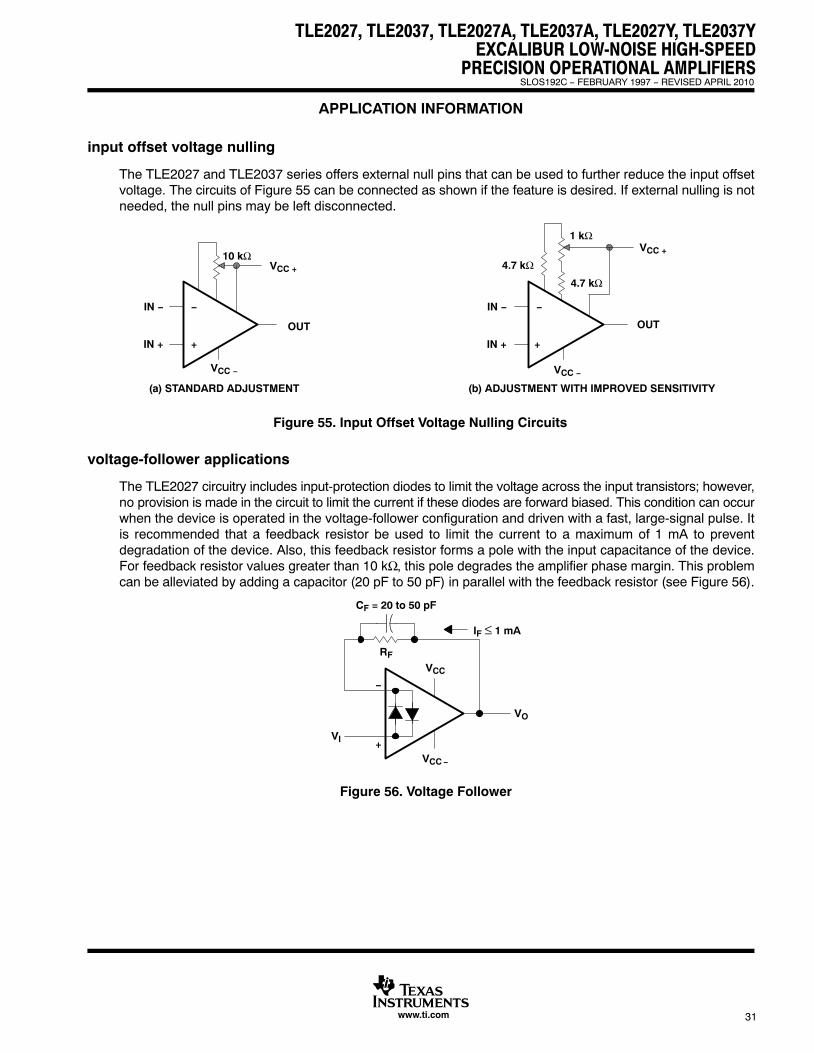
input offset voltage nulling
The TLE2027 and TLE2037 series offers external null pins that can be used to further reduce the input offsetvoltage. The circuits of Figure 55 can be connected as shown if the feature is desired. If external nulling is notneeded, the null pins may be left disconnected.
4.7 kΩ
1 kΩVCC +
OUT
IN −
IN +
VCC −
+
−
4.7 kΩ
−
+
VCC −
OUT
VCC +10 kΩ
IN −
IN +
(a) STANDARD ADJUSTMENT (b) ADJUSTMENT WITH IMPROVED SENSITIVITY
Figure 55. Input Offset Voltage Nulling Circuits
voltage-follower applications
The TLE2027 circuitry includes input-protection diodes to limit the voltage across the input transistors; however,no provision is made in the circuit to limit the current if these diodes are forward biased. This condition can occurwhen the device is operated in the voltage-follower configuration and driven with a fast, large-signal pulse. Itis recommended that a feedback resistor be used to limit the current to a maximum of 1 mA to preventdegradation of the device. Also, this feedback resistor forms a pole with the input capacitance of the device.For feedback resistor values greater than 10 kΩ, this pole degrades the amplifier phase margin. This problemcan be alleviated by adding a capacitor (20 pF to 50 pF) in parallel with the feedback resistor (see Figure 56).
RF
IF ≤ 1 mA
−
+VI
VO
VCC−
VCC
CF = 20 to 50 pF
Figure 56. Voltage Follower
TLE2027, TLE2037, TLE2027A, TLE2037A, TLE2027Y, TLE2037YEXCALIBUR LOW-NOISE HIGH-SPEEDPRECISION OPERATIONAL AMPLIFIERS
�
SLOS192C − FEBRUARY 1997 − REVISED APRIL 2010
32 www.ti.com
APPLICATION INFORMATION
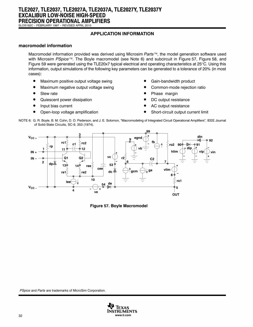
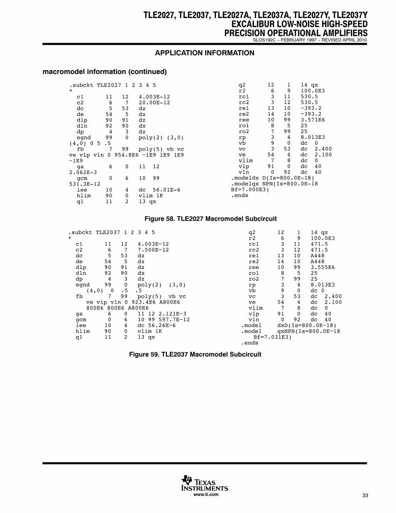
macromodel information
Macromodel information provided was derived using Microsim Parts™, the model generation software usedwith Microsim PSpice™. The Boyle macromodel (see Note 6) and subcircuit in Figure 57, Figure 58, andFigure 59 were generated using the TLE20x7 typical electrical and operating characteristics at 25°C. Using thisinformation, output simulations of the following key parameters can be generated to a tolerance of 20% (in mostcases):
• Maximum positive output voltage swing
• Maximum negative output voltage swing
• Slew rate
• Quiescent power dissipation
• Input bias current
• Open-loop voltage amplification
• Gain-bandwidth product
• Common-mode rejection ratio
• Phase margin
• DC output resistance
• AC output resistance
• Short-circuit output current limit
NOTE 6: G. R. Boyle, B. M. Cohn, D. O. Pederson, and J. E. Solomon, “Macromodeling of Integrated Circuit Operational Amplifiers”, IEEE Journalof Solid-State Circuits, SC-9, 353 (1974).
8
ro2
7
12
VCC +
IN +
IN −
VCC −
1
2 dp
rp11
rc1 c1 rc2
Q2Q1
13 14
3
re1 re2
4
lee
ve− +
5410
reecee
53
vc+
−r2
6
gcm ga
de
dc
vb
9
+
−
egnd
99+
− fb
C2
vlim+
−
ro1
5
OUT
90
hlim+ dip
−
9192
dln
vip vin+
− +
−
Figure 57. Boyle Macromodel
PSpice and Parts are trademarks of MicroSim Corporation.
TLE2027, TLE2037, TLE2027A, TLE2037A, TLE2027Y, TLE2037YEXCALIBUR LOW-NOISE HIGH-SPEED
PRECISION OPERATIONAL AMPLIFIERS
�
SLOS192C − FEBRUARY 1997 − REVISED APRIL 2010
33www.ti.com
APPLICATION INFORMATION
macromodel information (continued)
.subckt TLE2027 1 2 3 4 5*
c1 11 12 4.003E-12c2 6 7 20.00E-12dc 5 53 dzde 54 5 dzdlp 90 91 dzdln 92 90 dxdp 4 3 dzegnd 99 0 poly(2) (3,0)
(4,0) 0 5 .5fb 7 99 poly(5) vb vc
ve vlp vln 0 954.8E6 −1E9 1E9 1E9−1E9
ga 6 0 11 122.062E-3
gcm 0 6 10 99531.3E-12
iee 10 4 dc 56.01E-6hlim 90 0 vlim 1Kq1 11 2 13 qx
Figure 58. TLE2027 Macromodel Subcircuit
q2 12 1 14 qxr2 6 9 100.0E3rc1 3 11 530.5rc2 3 12 530.5re1 13 10 −393.2re2 14 10 −393.2ree 10 99 3.571E6ro1 8 5 25ro2 7 99 25rp 3 4 8.013E3vb 9 0 dc 0vc 3 53 dc 2.400ve 54 4 dc 2.100vlim 7 8 dc 0vlp 91 0 dc 40vln 0 92 dc 40
.modeldx D(Is=800.0E-18)
.modelqx NPN(Is=800.0E-18Bf=7.000E3).ends
.subckt TLE2037 1 2 3 4 5*
c1 11 12 4.003E−12c2 6 7 7.500E−12dc 5 53 dzde 54 5 dzdlp 90 91 dzdln 92 90 dxdp 4 3 dzegnd 99 0 poly(2) (3,0) (4,0) 0 .5 .5fb 7 99 poly(5) vb vc ve vip vln 0 923.4E6 A800E6 800E6 800E6 A800E6ga 6 0 11 12 2.121E−3gcm 0 6 10 99 597.7E−12iee 10 4 dc 56.26E−6hlim 90 0 vlim 1Kq1 11 2 13 qx
Figure 59. TLE2037 Macromodel Subcircuit
q2 12 1 14 qzr2 6 9 100.0E3rc1 3 11 471.5rc2 3 12 471.5re1 13 10 A448re2 14 10 A448ree 10 99 3.555E6ro1 8 5 25ro2 7 99 25rp 3 4 8.013E3vb 9 0 dc 0vc 3 53 dc 2.400ve 54 4 dc 2.100vlim 7 8 dc 0vlp 91 0 dc 40vln 0 92 dc 40
.model dxD(Is=800.0E−18)
.model qxNPN(Is=800.0E−18 Bf=7.031E3)
.ends
TLE2027, TLE2037, TLE2027A, TLE2037A, TLE2027Y, TLE2037YEXCALIBUR LOW-NOISE HIGH-SPEEDPRECISION OPERATIONAL AMPLIFIERS
�
SLOS192C − FEBRUARY 1997 − REVISED APRIL 2010
34 www.ti.com
REVISION HISTORY
Changes from Revision B (October 2006) to Revision C
• Changed values of Vn, VN(PP), and In . . . . . . . . . . . . . . . . . . . . . . . . . . . . . . . . . . . . . . . . . . . . .. . . 11
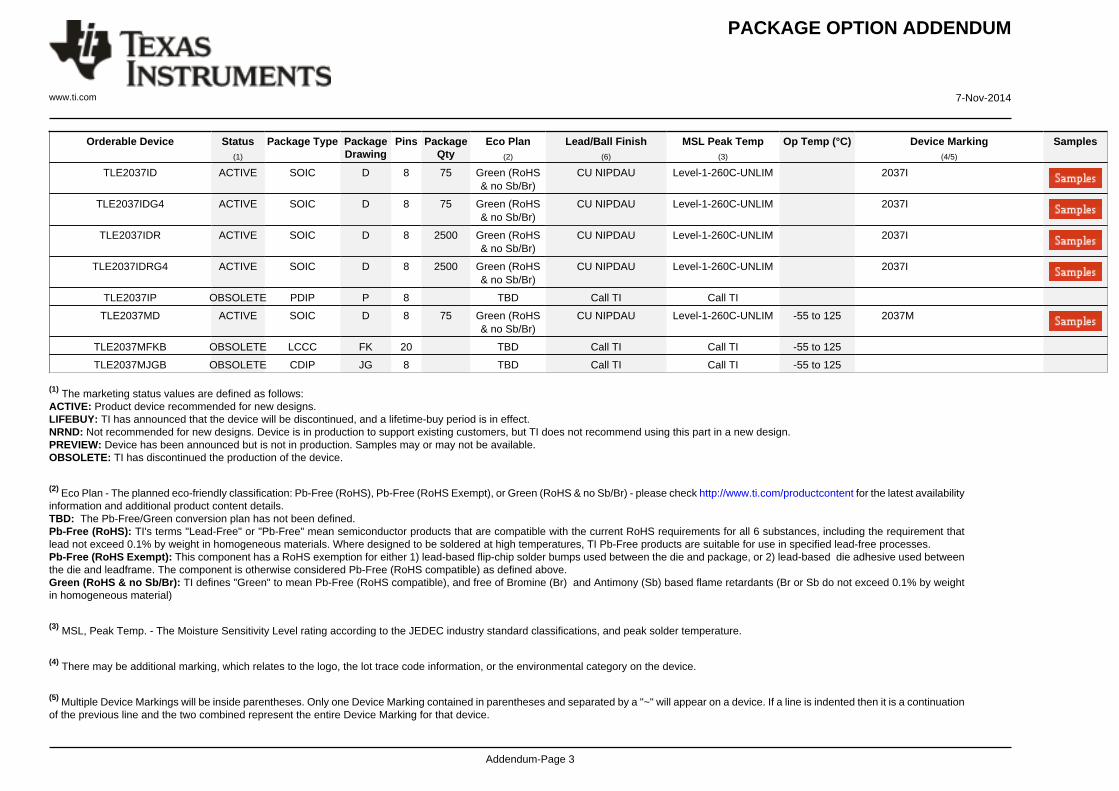
PACKAGE OPTION ADDENDUM
www.ti.com 7-Nov-2014
Addendum-Page 1
PACKAGING INFORMATION
Orderable Device Status(1)
Package Type PackageDrawing
Pins PackageQty
Eco Plan(2)
Lead/Ball Finish(6)
MSL Peak Temp(3)
Op Temp (°C) Device Marking(4/5)
Samples
5962-9089601M2A ACTIVE LCCC FK 20 1 TBD POST-PLATE N / A for Pkg Type -55 to 125 5962-9089601M2ATLE2027MFKB
5962-9089601MPA ACTIVE CDIP JG 8 1 TBD A42 N / A for Pkg Type -55 to 125 9089601MPATLE2027M
5962-9089602MPA OBSOLETE CDIP JG 8 TBD Call TI Call TI -55 to 125
5962-9089603Q2A ACTIVE LCCC FK 20 1 TBD POST-PLATE N / A for Pkg Type -55 to 125 5962-9089603Q2ATLE2027AMFKB
5962-9089603QPA ACTIVE CDIP JG 8 1 TBD A42 N / A for Pkg Type -55 to 125 9089603QPATLE2027AM
TLE2027ACD OBSOLETE SOIC D 8 TBD Call TI Call TI
TLE2027ACP OBSOLETE PDIP P 8 TBD Call TI Call TI
TLE2027AID OBSOLETE SOIC D 8 TBD Call TI Call TI
TLE2027AIP OBSOLETE PDIP P 8 TBD Call TI Call TI
TLE2027AMD ACTIVE SOIC D 8 75 Green (RoHS& no Sb/Br)
CU NIPDAU Level-1-260C-UNLIM -55 to 125 2027AM
TLE2027AMDG4 ACTIVE SOIC D 8 75 Green (RoHS& no Sb/Br)
CU NIPDAU Level-1-260C-UNLIM 2027AM
TLE2027AMFKB ACTIVE LCCC FK 20 1 TBD POST-PLATE N / A for Pkg Type -55 to 125 5962-9089603Q2ATLE2027AMFKB
TLE2027AMJG ACTIVE CDIP JG 8 1 TBD A42 N / A for Pkg Type -55 to 125 TLE2027AMJG
TLE2027AMJGB ACTIVE CDIP JG 8 1 TBD A42 N / A for Pkg Type -55 to 125 9089603QPATLE2027AM
TLE2027CD ACTIVE SOIC D 8 75 Green (RoHS& no Sb/Br)
CU NIPDAU Level-1-260C-UNLIM 2027C
TLE2027CDG4 ACTIVE SOIC D 8 75 Green (RoHS& no Sb/Br)
CU NIPDAU Level-1-260C-UNLIM 2027C
TLE2027CDR ACTIVE SOIC D 8 2500 Green (RoHS& no Sb/Br)
CU NIPDAU Level-1-260C-UNLIM 2027C
TLE2027CDRG4 ACTIVE SOIC D 8 TBD Call TI Call TI
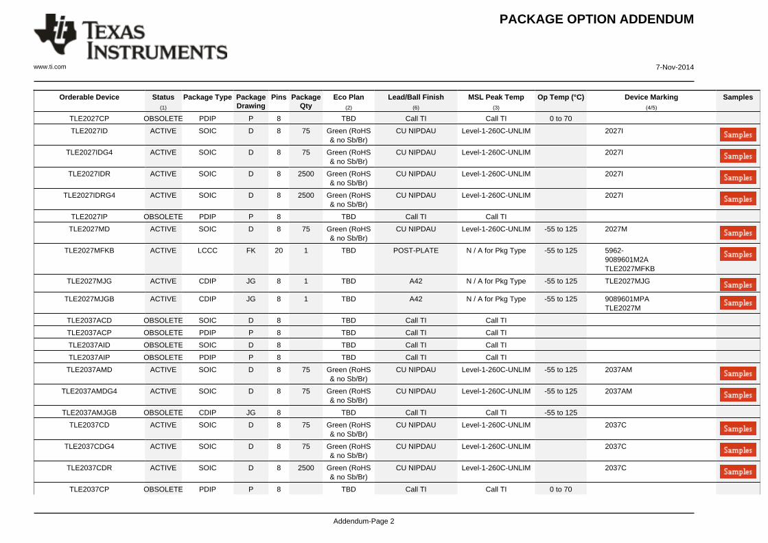
PACKAGE OPTION ADDENDUM
www.ti.com 7-Nov-2014
Addendum-Page 2
Orderable Device Status(1)
Package Type PackageDrawing
Pins PackageQty
Eco Plan(2)
Lead/Ball Finish(6)
MSL Peak Temp(3)
Op Temp (°C) Device Marking(4/5)
Samples
TLE2027CP OBSOLETE PDIP P 8 TBD Call TI Call TI 0 to 70
TLE2027ID ACTIVE SOIC D 8 75 Green (RoHS& no Sb/Br)
CU NIPDAU Level-1-260C-UNLIM 2027I
TLE2027IDG4 ACTIVE SOIC D 8 75 Green (RoHS& no Sb/Br)
CU NIPDAU Level-1-260C-UNLIM 2027I
TLE2027IDR ACTIVE SOIC D 8 2500 Green (RoHS& no Sb/Br)
CU NIPDAU Level-1-260C-UNLIM 2027I
TLE2027IDRG4 ACTIVE SOIC D 8 2500 Green (RoHS& no Sb/Br)
CU NIPDAU Level-1-260C-UNLIM 2027I
TLE2027IP OBSOLETE PDIP P 8 TBD Call TI Call TI
TLE2027MD ACTIVE SOIC D 8 75 Green (RoHS& no Sb/Br)
CU NIPDAU Level-1-260C-UNLIM -55 to 125 2027M
TLE2027MFKB ACTIVE LCCC FK 20 1 TBD POST-PLATE N / A for Pkg Type -55 to 125 5962-9089601M2ATLE2027MFKB
TLE2027MJG ACTIVE CDIP JG 8 1 TBD A42 N / A for Pkg Type -55 to 125 TLE2027MJG
TLE2027MJGB ACTIVE CDIP JG 8 1 TBD A42 N / A for Pkg Type -55 to 125 9089601MPATLE2027M
TLE2037ACD OBSOLETE SOIC D 8 TBD Call TI Call TI
TLE2037ACP OBSOLETE PDIP P 8 TBD Call TI Call TI
TLE2037AID OBSOLETE SOIC D 8 TBD Call TI Call TI
TLE2037AIP OBSOLETE PDIP P 8 TBD Call TI Call TI
TLE2037AMD ACTIVE SOIC D 8 75 Green (RoHS& no Sb/Br)
CU NIPDAU Level-1-260C-UNLIM -55 to 125 2037AM
TLE2037AMDG4 ACTIVE SOIC D 8 75 Green (RoHS& no Sb/Br)
CU NIPDAU Level-1-260C-UNLIM -55 to 125 2037AM
TLE2037AMJGB OBSOLETE CDIP JG 8 TBD Call TI Call TI -55 to 125
TLE2037CD ACTIVE SOIC D 8 75 Green (RoHS& no Sb/Br)
CU NIPDAU Level-1-260C-UNLIM 2037C
TLE2037CDG4 ACTIVE SOIC D 8 75 Green (RoHS& no Sb/Br)
CU NIPDAU Level-1-260C-UNLIM 2037C
TLE2037CDR ACTIVE SOIC D 8 2500 Green (RoHS& no Sb/Br)
CU NIPDAU Level-1-260C-UNLIM 2037C
TLE2037CP OBSOLETE PDIP P 8 TBD Call TI Call TI 0 to 70
PACKAGE OPTION ADDENDUM
www.ti.com 7-Nov-2014
Addendum-Page 3
Orderable Device Status(1)
Package Type PackageDrawing
Pins PackageQty
Eco Plan(2)
Lead/Ball Finish(6)
MSL Peak Temp(3)
Op Temp (°C) Device Marking(4/5)
Samples
TLE2037ID ACTIVE SOIC D 8 75 Green (RoHS& no Sb/Br)
CU NIPDAU Level-1-260C-UNLIM 2037I
TLE2037IDG4 ACTIVE SOIC D 8 75 Green (RoHS& no Sb/Br)
CU NIPDAU Level-1-260C-UNLIM 2037I
TLE2037IDR ACTIVE SOIC D 8 2500 Green (RoHS& no Sb/Br)
CU NIPDAU Level-1-260C-UNLIM 2037I
TLE2037IDRG4 ACTIVE SOIC D 8 2500 Green (RoHS& no Sb/Br)
CU NIPDAU Level-1-260C-UNLIM 2037I
TLE2037IP OBSOLETE PDIP P 8 TBD Call TI Call TI
TLE2037MD ACTIVE SOIC D 8 75 Green (RoHS& no Sb/Br)
CU NIPDAU Level-1-260C-UNLIM -55 to 125 2037M
TLE2037MFKB OBSOLETE LCCC FK 20 TBD Call TI Call TI -55 to 125
TLE2037MJGB OBSOLETE CDIP JG 8 TBD Call TI Call TI -55 to 125 (1) The marketing status values are defined as follows:ACTIVE: Product device recommended for new designs.LIFEBUY: TI has announced that the device will be discontinued, and a lifetime-buy period is in effect.NRND: Not recommended for new designs. Device is in production to support existing customers, but TI does not recommend using this part in a new design.PREVIEW: Device has been announced but is not in production. Samples may or may not be available.OBSOLETE: TI has discontinued the production of the device.
(2) Eco Plan - The planned eco-friendly classification: Pb-Free (RoHS), Pb-Free (RoHS Exempt), or Green (RoHS & no Sb/Br) - please check http://www.ti.com/productcontent for the latest availabilityinformation and additional product content details.TBD: The Pb-Free/Green conversion plan has not been defined.Pb-Free (RoHS): TI's terms "Lead-Free" or "Pb-Free" mean semiconductor products that are compatible with the current RoHS requirements for all 6 substances, including the requirement thatlead not exceed 0.1% by weight in homogeneous materials. Where designed to be soldered at high temperatures, TI Pb-Free products are suitable for use in specified lead-free processes.Pb-Free (RoHS Exempt): This component has a RoHS exemption for either 1) lead-based flip-chip solder bumps used between the die and package, or 2) lead-based die adhesive used betweenthe die and leadframe. The component is otherwise considered Pb-Free (RoHS compatible) as defined above.Green (RoHS & no Sb/Br): TI defines "Green" to mean Pb-Free (RoHS compatible), and free of Bromine (Br) and Antimony (Sb) based flame retardants (Br or Sb do not exceed 0.1% by weightin homogeneous material)
(3) MSL, Peak Temp. - The Moisture Sensitivity Level rating according to the JEDEC industry standard classifications, and peak solder temperature.
(4) There may be additional marking, which relates to the logo, the lot trace code information, or the environmental category on the device.
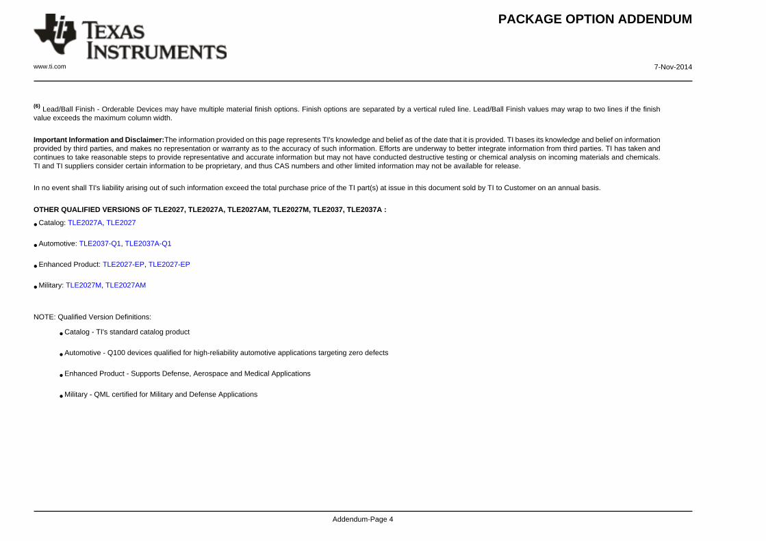
(5) Multiple Device Markings will be inside parentheses. Only one Device Marking contained in parentheses and separated by a "~" will appear on a device. If a line is indented then it is a continuationof the previous line and the two combined represent the entire Device Marking for that device.
PACKAGE OPTION ADDENDUM
www.ti.com 7-Nov-2014
Addendum-Page 4
(6) Lead/Ball Finish - Orderable Devices may have multiple material finish options. Finish options are separated by a vertical ruled line. Lead/Ball Finish values may wrap to two lines if the finishvalue exceeds the maximum column width.
Important Information and Disclaimer:The information provided on this page represents TI's knowledge and belief as of the date that it is provided. TI bases its knowledge and belief on informationprovided by third parties, and makes no representation or warranty as to the accuracy of such information. Efforts are underway to better integrate information from third parties. TI has taken andcontinues to take reasonable steps to provide representative and accurate information but may not have conducted destructive testing or chemical analysis on incoming materials and chemicals.TI and TI suppliers consider certain information to be proprietary, and thus CAS numbers and other limited information may not be available for release.
In no event shall TI's liability arising out of such information exceed the total purchase price of the TI part(s) at issue in this document sold by TI to Customer on an annual basis.
OTHER QUALIFIED VERSIONS OF TLE2027, TLE2027A, TLE2027AM, TLE2027M, TLE2037, TLE2037A :
• Catalog: TLE2027A, TLE2027
• Automotive: TLE2037-Q1, TLE2037A-Q1
• Enhanced Product: TLE2027-EP, TLE2027-EP
• Military: TLE2027M, TLE2027AM
NOTE: Qualified Version Definitions:
• Catalog - TI's standard catalog product
• Automotive - Q100 devices qualified for high-reliability automotive applications targeting zero defects
• Enhanced Product - Supports Defense, Aerospace and Medical Applications
• Military - QML certified for Military and Defense Applications
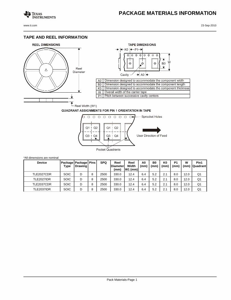
TAPE AND REEL INFORMATION
*All dimensions are nominal
Device PackageType
PackageDrawing
Pins SPQ ReelDiameter
(mm)
ReelWidth
W1 (mm)
A0(mm)
B0(mm)
K0(mm)
P1(mm)
W(mm)
Pin1Quadrant
TLE2027CDR SOIC D 8 2500 330.0 12.4 6.4 5.2 2.1 8.0 12.0 Q1
TLE2027IDR SOIC D 8 2500 330.0 12.4 6.4 5.2 2.1 8.0 12.0 Q1
TLE2037CDR SOIC D 8 2500 330.0 12.4 6.4 5.2 2.1 8.0 12.0 Q1
TLE2037IDR SOIC D 8 2500 330.0 12.4 6.4 5.2 2.1 8.0 12.0 Q1
PACKAGE MATERIALS INFORMATION
www.ti.com 23-Sep-2010
Pack Materials-Page 1
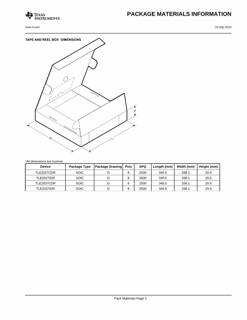
*All dimensions are nominal
Device Package Type Package Drawing Pins SPQ Length (mm) Width (mm) Height (mm)
TLE2027CDR SOIC D 8 2500 340.5 338.1 20.6
TLE2027IDR SOIC D 8 2500 340.5 338.1 20.6
TLE2037CDR SOIC D 8 2500 340.5 338.1 20.6
TLE2037IDR SOIC D 8 2500 340.5 338.1 20.6
PACKAGE MATERIALS INFORMATION
www.ti.com 23-Sep-2010
Pack Materials-Page 2
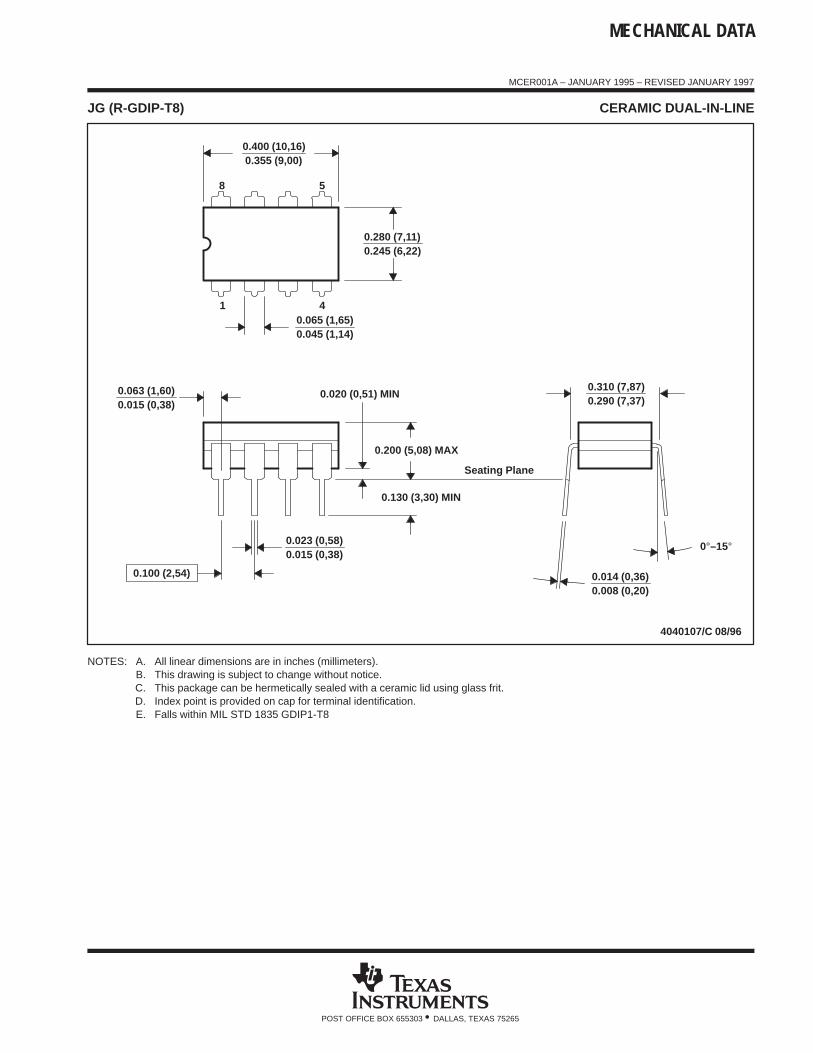
MECHANICAL DATA
MCER001A – JANUARY 1995 – REVISED JANUARY 1997
POST OFFICE BOX 655303 • DALLAS, TEXAS 75265
JG (R-GDIP-T8) CERAMIC DUAL-IN-LINE
0.310 (7,87)0.290 (7,37)
0.014 (0,36)0.008 (0,20)
Seating Plane
4040107/C 08/96
5
40.065 (1,65)0.045 (1,14)
8
1
0.020 (0,51) MIN
0.400 (10,16)0.355 (9,00)
0.015 (0,38)0.023 (0,58)
0.063 (1,60)0.015 (0,38)
0.200 (5,08) MAX
0.130 (3,30) MIN
0.245 (6,22)0.280 (7,11)
0.100 (2,54)
0°–15°
NOTES: A. All linear dimensions are in inches (millimeters).B. This drawing is subject to change without notice.C. This package can be hermetically sealed with a ceramic lid using glass frit.D. Index point is provided on cap for terminal identification.E. Falls within MIL STD 1835 GDIP1-T8
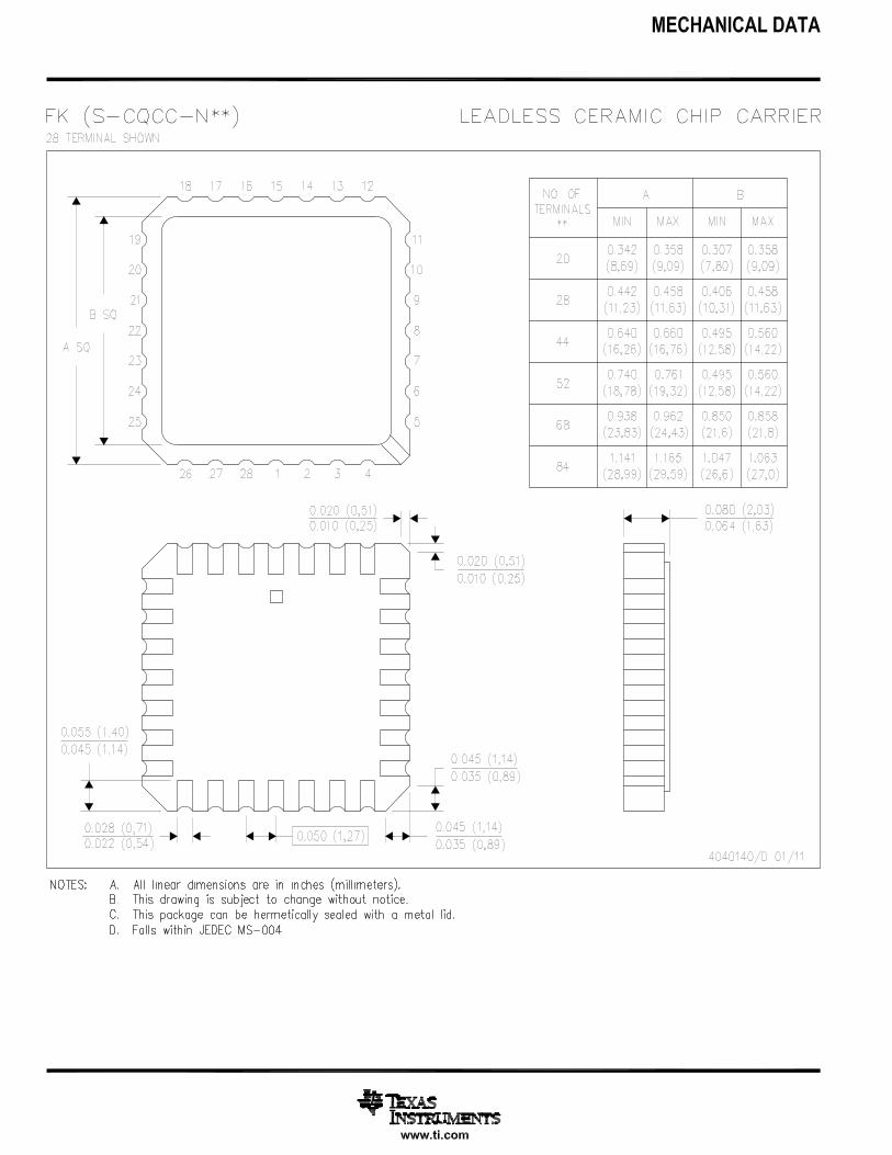
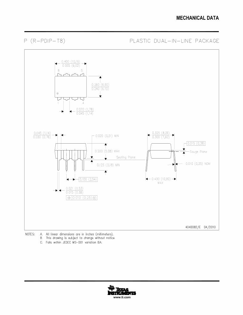
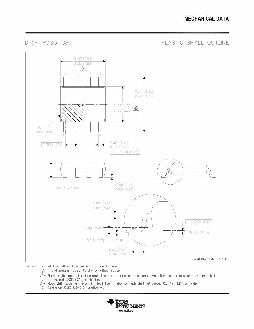
IMPORTANT NOTICETexas Instruments Incorporated and its subsidiaries (TI) reserve the right to make corrections, enhancements, improvements and otherchanges to its semiconductor products and services per JESD46, latest issue, and to discontinue any product or service per JESD48, latestissue. Buyers should obtain the latest relevant information before placing orders and should verify that such information is current andcomplete. All semiconductor products (also referred to herein as “components”) are sold subject to TI’s terms and conditions of salesupplied at the time of order acknowledgment.TI warrants performance of its components to the specifications applicable at the time of sale, in accordance with the warranty in TI’s termsand conditions of sale of semiconductor products. Testing and other quality control techniques are used to the extent TI deems necessaryto support this warranty. Except where mandated by applicable law, testing of all parameters of each component is not necessarilyperformed.TI assumes no liability for applications assistance or the design of Buyers’ products. Buyers are responsible for their products andapplications using TI components. To minimize the risks associated with Buyers’ products and applications, Buyers should provideadequate design and operating safeguards.TI does not warrant or represent that any license, either express or implied, is granted under any patent right, copyright, mask work right, orother intellectual property right relating to any combination, machine, or process in which TI components or services are used. Informationpublished by TI regarding third-party products or services does not constitute a license to use such products or services or a warranty orendorsement thereof. Use of such information may require a license from a third party under the patents or other intellectual property of thethird party, or a license from TI under the patents or other intellectual property of TI.Reproduction of significant portions of TI information in TI data books or data sheets is permissible only if reproduction is without alterationand is accompanied by all associated warranties, conditions, limitations, and notices. TI is not responsible or liable for such altereddocumentation. Information of third parties may be subject to additional restrictions.Resale of TI components or services with statements different from or beyond the parameters stated by TI for that component or servicevoids all express and any implied warranties for the associated TI component or service and is an unfair and deceptive business practice.TI is not responsible or liable for any such statements.Buyer acknowledges and agrees that it is solely responsible for compliance with all legal, regulatory and safety-related requirementsconcerning its products, and any use of TI components in its applications, notwithstanding any applications-related information or supportthat may be provided by TI. Buyer represents and agrees that it has all the necessary expertise to create and implement safeguards whichanticipate dangerous consequences of failures, monitor failures and their consequences, lessen the likelihood of failures that might causeharm and take appropriate remedial actions. Buyer will fully indemnify TI and its representatives against any damages arising out of the useof any TI components in safety-critical applications.In some cases, TI components may be promoted specifically to facilitate safety-related applications. With such components, TI’s goal is tohelp enable customers to design and create their own end-product solutions that meet applicable functional safety standards andrequirements. Nonetheless, such components are subject to these terms.No TI components are authorized for use in FDA Class III (or similar life-critical medical equipment) unless authorized officers of the partieshave executed a special agreement specifically governing such use.Only those TI components which TI has specifically designated as military grade or “enhanced plastic” are designed and intended for use inmilitary/aerospace applications or environments. Buyer acknowledges and agrees that any military or aerospace use of TI componentswhich have not been so designated is solely at the Buyer's risk, and that Buyer is solely responsible for compliance with all legal andregulatory requirements in connection with such use.TI has specifically designated certain components as meeting ISO/TS16949 requirements, mainly for automotive use. In any case of use ofnon-designated products, TI will not be responsible for any failure to meet ISO/TS16949.Products ApplicationsAudio www.ti.com/audio Automotive and Transportation www.ti.com/automotiveAmplifiers amplifier.ti.com Communications and Telecom www.ti.com/communicationsData Converters dataconverter.ti.com Computers and Peripherals www.ti.com/computersDLP® Products www.dlp.com Consumer Electronics www.ti.com/consumer-appsDSP dsp.ti.com Energy and Lighting www.ti.com/energyClocks and Timers www.ti.com/clocks Industrial www.ti.com/industrialInterface interface.ti.com Medical www.ti.com/medicalLogic logic.ti.com Security www.ti.com/securityPower Mgmt power.ti.com Space, Avionics and Defense www.ti.com/space-avionics-defenseMicrocontrollers microcontroller.ti.com Video and Imaging www.ti.com/videoRFID www.ti-rfid.comOMAP Applications Processors www.ti.com/omap TI E2E Community e2e.ti.comWireless Connectivity www.ti.com/wirelessconnectivity
Mailing Address: Texas Instruments, Post Office Box 655303, Dallas, Texas 75265Copyright © 2014, Texas Instruments Incorporated

![CD4541B (Rev. E) · 2017. 5. 30. · Title: CD4541B (Rev. E) Author: Texas Instruments, Incorporated [SCHS085,E ] Subject: Data Sheet Keywords: SCHS085,SCHS085E,SCHS085 Created Date:](https://static.fdocument.org/doc/165x107/60d4c35990a1b102c8742d51/cd4541b-rev-e-2017-5-30-title-cd4541b-rev-e-author-texas-instruments.jpg)