Evolution, substrate specificity and subfamily classification of
. Contact: [email protected]. Andideh 2003 MIT
1
Evaluation and Evolution of Low κInter-Layer Dielectric (ILD) Material
and Integration Schemes
Dr. Eb AndidehIntel Corporation
Logic Technology Development
.E. Andideh 2003 MIT
2
• I am neither a Chemical Engineer nor a Material Scientist
– I am an Electrical Engineer with expertise in microfabrication process development
Disclaimer
.E. Andideh 2003 MIT
3
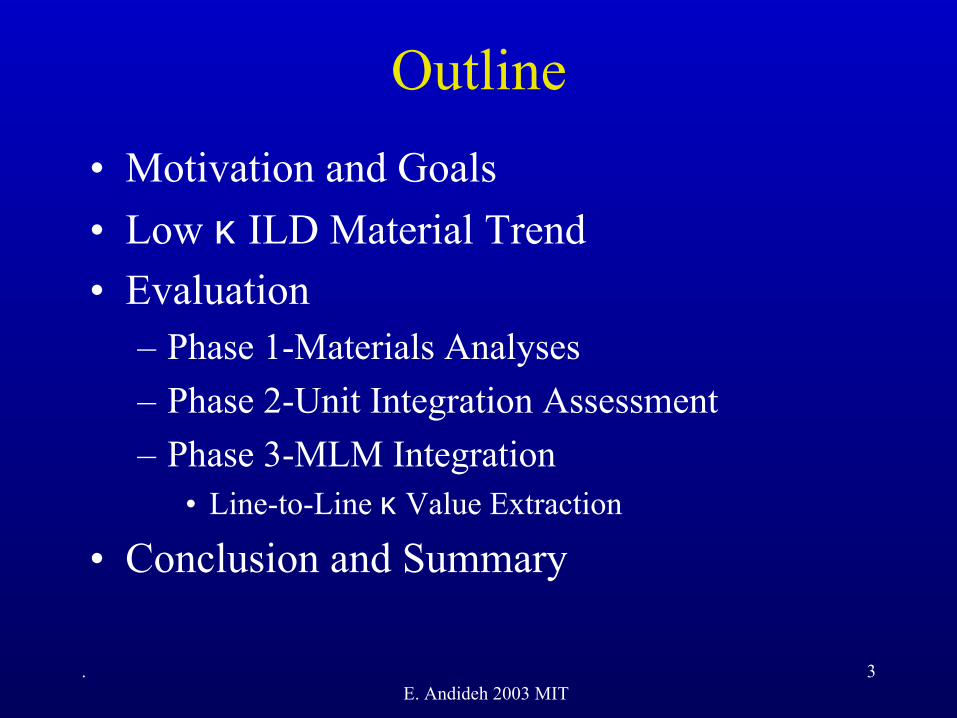
Outline• Motivation and Goals• Low κ ILD Material Trend• Evaluation
– Phase 1-Materials Analyses– Phase 2-Unit Integration Assessment– Phase 3-MLM Integration
• Line-to-Line κ Value Extraction
• Conclusion and Summary
.E. Andideh 2003 MIT
4
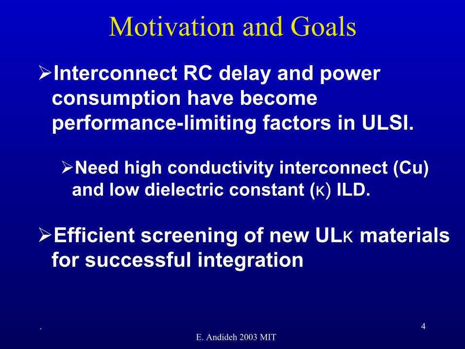
Motivation and GoalsInterconnect RC delay and power consumption have become performance-limiting factors in ULSI.
Need high conductivity interconnect (Cu) and low dielectric constant (κ) ILD.
Efficient screening of new ULκ materials for successful integration
.E. Andideh 2003 MIT
5
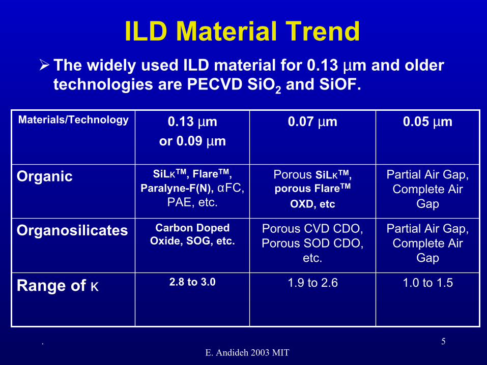
ILD Material Trend
1.0 to 1.51.9 to 2.62.8 to 3.0Range of κ
Partial Air Gap, Complete Air
Gap
Porous CVD CDO, Porous SOD CDO,
etc.
Carbon Doped Oxide, SOG, etc.
Organosilicates
Partial Air Gap, Complete Air
Gap
Porous SiLκTM, porous FlareTM
OXD, etc
SiLκTM, FlareTM, Paralyne-F(N), αFC,
PAE, etc.
Organic
0.05 µm0.07 µm0.13 µmor 0.09 µm
Materials/Technology
The widely used ILD material for 0.13 µm and older technologies are PECVD SiO2 and SiOF.
.E. Andideh 2003 MIT
6
Decreasing the Dielectric ConstantLowering the material density
Add Porosity (air) or lighter elementsκ decreases due to κair~1Thermal-Mechanical properties degradePore size and pore connectivity is a major integration concern
Lowering the polarizability of bondsReduce number of Si-O bondsInclude Si-F or Si-C bonds in filmOrganic materials such as Teflon.Outgassing, adhesion and other TM properties degrade.
.E. Andideh 2003 MIT
7
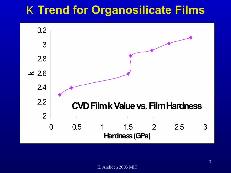
κ Trend for Organosilicate Films
CVD Film k Value vs. Film Hardness2
2.2
2.4
2.6
2.8
3
3.2
0 0.5 1 1.5 2 2.5 3Hardness (GPa)
k
.E. Andideh 2003 MIT
8
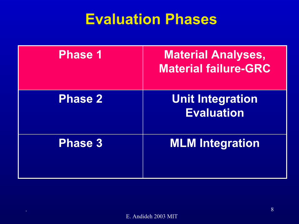
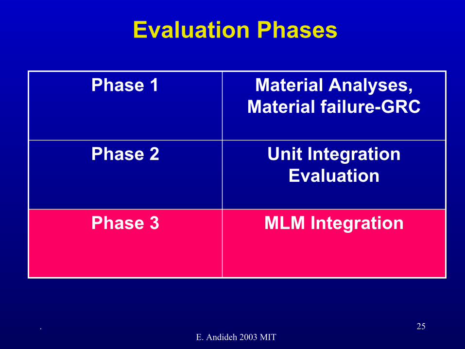
Evaluation Phases
MLM IntegrationPhase 3
Unit Integration Evaluation
Phase 2
Material Analyses, Material failure-GRC
Phase 1
.E. Andideh 2003 MIT
9
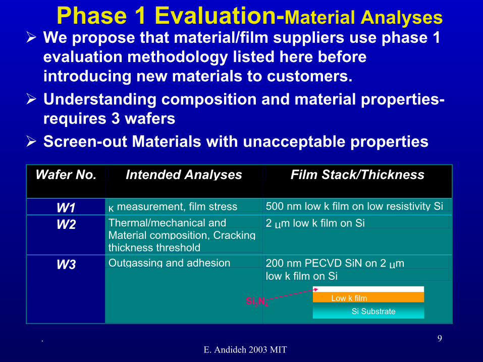
Phase 1 Evaluation-Material AnalysesWe propose that material/film suppliers use phase 1 evaluation methodology listed here before introducing new materials to customers.Understanding composition and material properties-requires 3 wafersScreen-out Materials with unacceptable properties
Wafer No. Intended Analyses Film Stack/Thickness
W1 κ measurement, film stress 500 nm low k film on low resistivity Si
W2 Thermal/mechanical and Material composition, Cracking thickness threshold
2 µm low k film on Si
W3 Outgassing and adhesion 200 nm PECVD SiN on 2 µm low k film on Si
Si SubstrateLow k filmSi3N4
.E. Andideh 2003 MIT
10
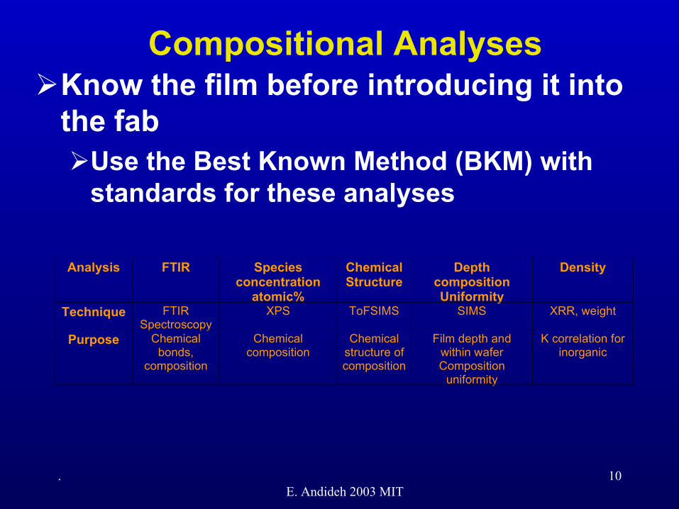
Compositional AnalysesKnow the film before introducing it into the fab
Use the Best Known Method (BKM) with standards for these analyses
Analysis FTIR Species concentration
atomic%
Chemical Structure
Depth composition Uniformity
Density
Technique FTIR Spectroscopy
XPS ToFSIMS SIMS XRR, weight
Purpose Chemical bonds,
composition
Chemical composition
Chemical structure of composition
Film depth and within wafer Composition
uniformity
K correlation for inorganic
.E. Andideh 2003 MIT
11
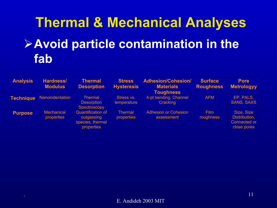
Thermal & Mechanical AnalysesAvoid particle contamination in the fab
Analysis Hardness/ Modulus
Thermal Desorption
Stress Hysteresis
Adhesion/Cohesion/Materials
Toughness
Surface Roughness
Pore Metrologyy
Technique Nanoindentation Thermal Desorption
Spectroscopy
Stress vs. temperature
4-pt bending, Channel Cracking
AFM EP, PALS, SANS, SAXS
Purpose Mechanical properties
Quantification of outgassing
species, thermal properties
Thermal properties
Adhesion or Cohesion assessment
Film roughness
Size, Size Distribution,
Connected or close pores
.E. Andideh 2003 MIT
12
Phase 1 Analyses-The κ
Is κ value acceptable for the current generation of technology?Is there a practical roadmap to improve κ?
κ extendibility for the next generation
.E. Andideh 2003 MIT
13
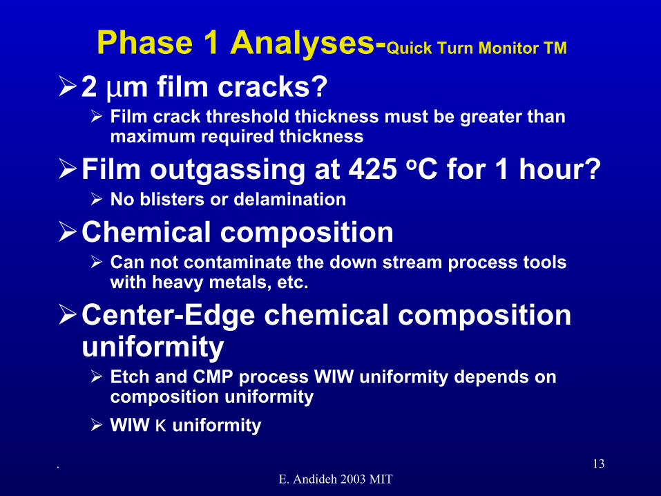
Phase 1 Analyses-Quick Turn Monitor TM
2 µm film cracks?Film crack threshold thickness must be greater than maximum required thickness
Film outgassing at 425 oC for 1 hour?No blisters or delamination
Chemical compositionCan not contaminate the down stream process tools with heavy metals, etc.
Center-Edge chemical composition uniformity
Etch and CMP process WIW uniformity depends on composition uniformityWIW κ uniformity
.E. Andideh 2003 MIT
14
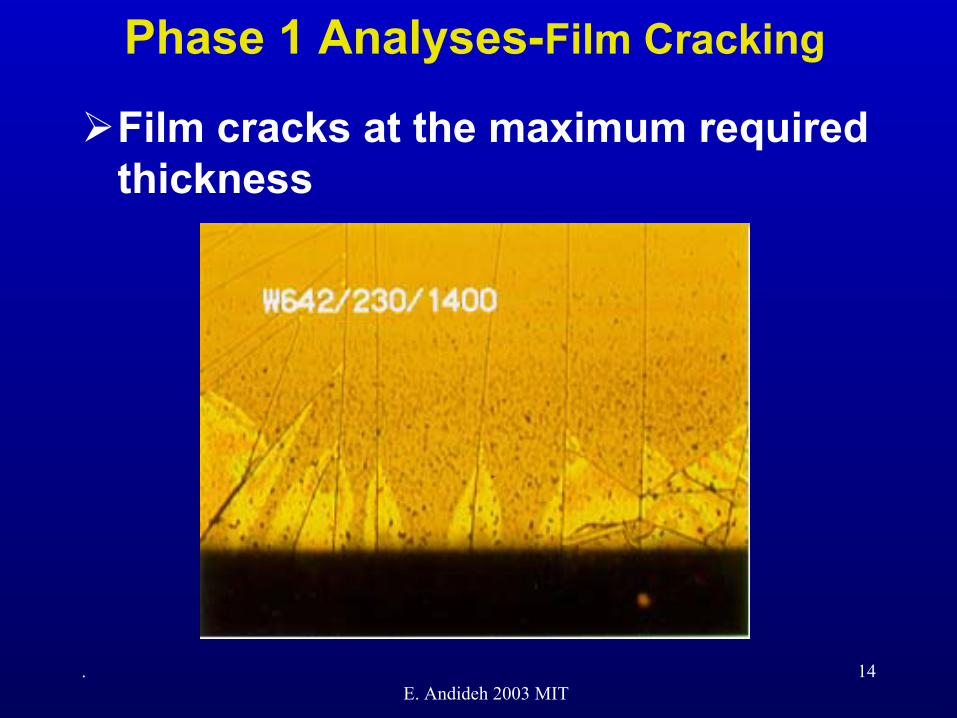
Phase 1 Analyses-Film Cracking
Film cracks at the maximum required thickness
.E. Andideh 2003 MIT
15
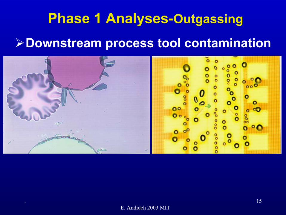
Phase 1 Analyses-Outgassing
Downstream process tool contamination
.E. Andideh 2003 MIT
16
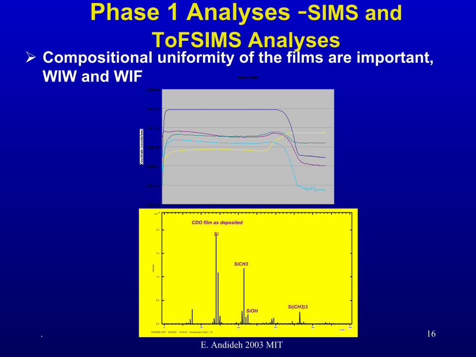
Phase 1 Analyses -SIMS and ToFSIMS Analyses
Wafer #863
1.00E+02
1.00E+03
1.00E+04
1.00E+05
1.00E+06
1.00E+07
1.00E+08
0 20 40 60 80 100 120 140 160
Depth (nm)
mass0 20 40 60 80 100
x10 6
0.0
0.5
1.0
1.5
2.0
inte
nsity
001634B1.DAT 06/20/00 13:40:48 Compression Factor : 23
Si
SiCH3
SiOH
CDO film as deposited
Si(CH3)3
Compositional uniformity of the films are important, WIW and WIF
.E. Andideh 2003 MIT
17
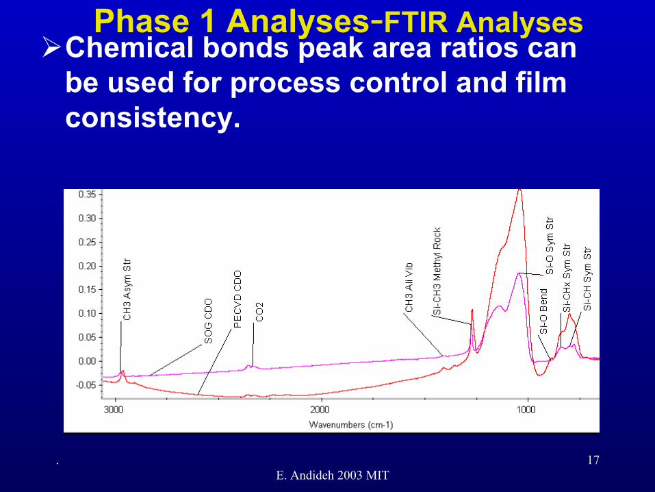
Phase 1 Analyses-FTIR AnalysesChemical bonds peak area ratios can be used for process control and film consistency.
.E. Andideh 2003 MIT
18
Evaluation Phases
MLM IntegrationPhase 3
Unit Module Integration Evaluation
Phase 2
Material Analyses, Material failure-GRC
Phase 1
.E. Andideh 2003 MIT
19
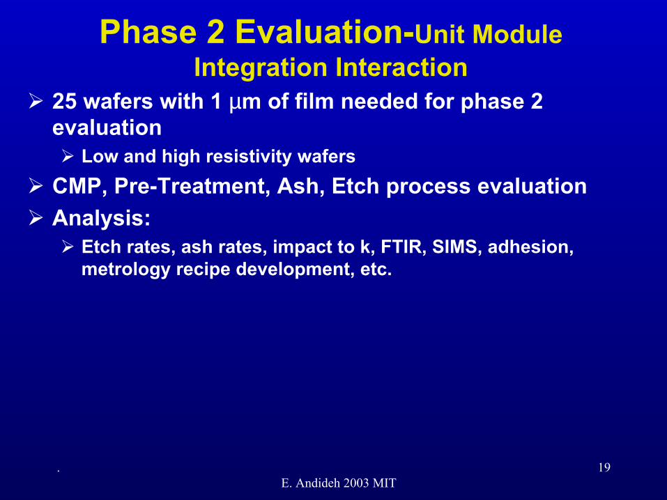
Phase 2 Evaluation-Unit Module Integration Interaction
25 wafers with 1 µm of film needed for phase 2 evaluation
Low and high resistivity wafersCMP, Pre-Treatment, Ash, Etch process evaluationAnalysis:
Etch rates, ash rates, impact to k, FTIR, SIMS, adhesion, metrology recipe development, etc.
.E. Andideh 2003 MIT
20
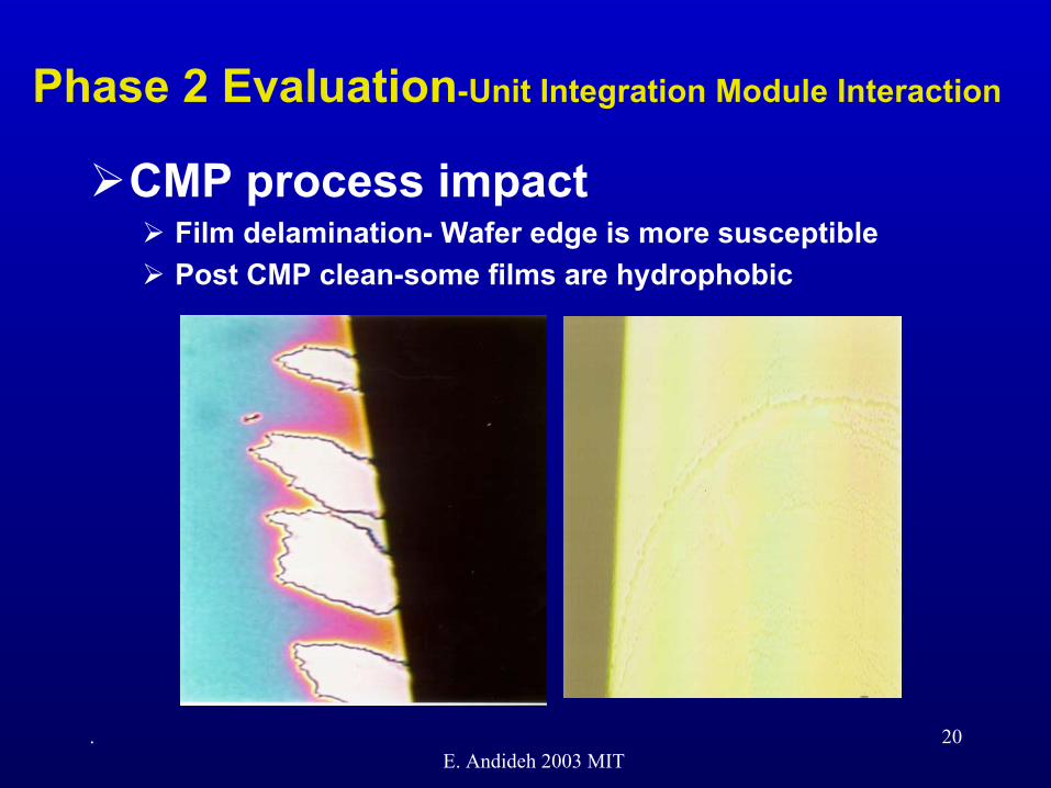
Phase 2 Evaluation-Unit Integration Module Interaction
CMP process impactFilm delamination- Wafer edge is more susceptiblePost CMP clean-some films are hydrophobic
.E. Andideh 2003 MIT
21
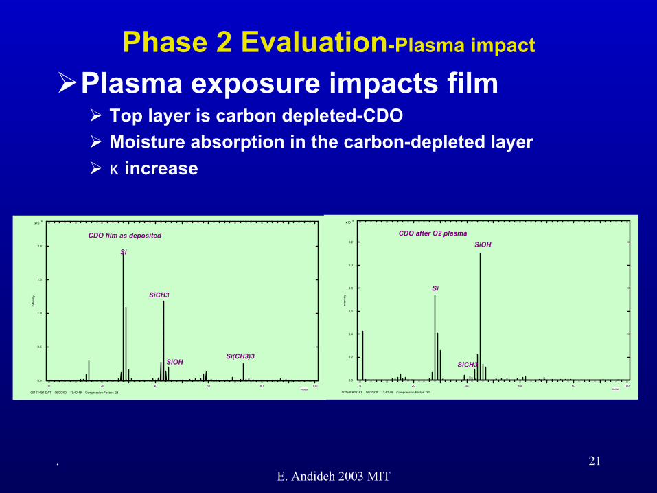
Phase 2 Evaluation-Plasma impact
Plasma exposure impacts filmTop layer is carbon depleted-CDOMoisture absorption in the carbon-depleted layerκ increase
mass0 20 40 60 80 100
x10 6
0.0
0.5
1.0
1.5
2.0
inte
nsity
001634B1.DAT 06/20/00 13:40:48 Compression Factor : 23
Si
SiCH3
SiOH
CDO film as deposited
Si(CH3)3
mass0 20 40 60 80 100
x10 6
0.0
0.2
0.4
0.6
0.8
1.0
1.2
inte
nsity
002548A2.DAT 06/20/00 13:47:49 Compression Factor : 22
Si
SiOH
SiCH3
CDO after O2 plasma
.E. Andideh 2003 MIT
22
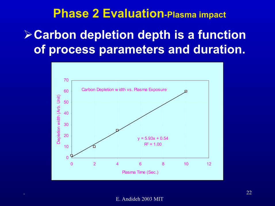
Phase 2 Evaluation-Plasma impact
Carbon Depletion w idth vs. Plasma Exposure
y = 5.93x + 0.54R2 = 1.00
0
10
20
30
40
50
60
70
0 2 4 6 8 10 12
Plasma Time (Sec.)
Dep
letio
n w
idth
(Arb
. Uni
t)
Carbon depletion depth is a function of process parameters and duration.
.E. Andideh 2003 MIT
23
Phase 2 Evaluation-κ MeasurementAccurate k measurement is essential for material selection
Mercury probe measured κ is only a relative value. More accurate measurement is required.CV dots deposited by shadow mask produces uncertain electrode area.A simple subtractive metal process with multiple size square dots produces the most accurate electrode area.Use of low resistivity wafer is recommended to avoid substrate damage by a plasma deposited film and to avoid substrate depletion capacitor complexity.Film thickness must be measured in close vicinity of the measured dots.
New materials may require accurate SEM/TEM thickness measurement.
.E. Andideh 2003 MIT
24
Adhesion of the new materials to hardmask, etch stop, and Cu diffusion barrier must be quantified with 4-pt bend.
Plasma, thermal or wet clean (Pretreatment) is required in most cases to improve adhesion to new materials.
Impact of pre-treatments on κ must be investigated.Avoidance of κ increase or means to restore the κvalue is required.
Phase 2 Evaluation-Adhesion
.E. Andideh 2003 MIT
25
Evaluation Phases
MLM IntegrationPhase 3
Unit Integration Evaluation
Phase 2
Material Analyses, Material failure-GRC
Phase 1
.E. Andideh 2003 MIT
26
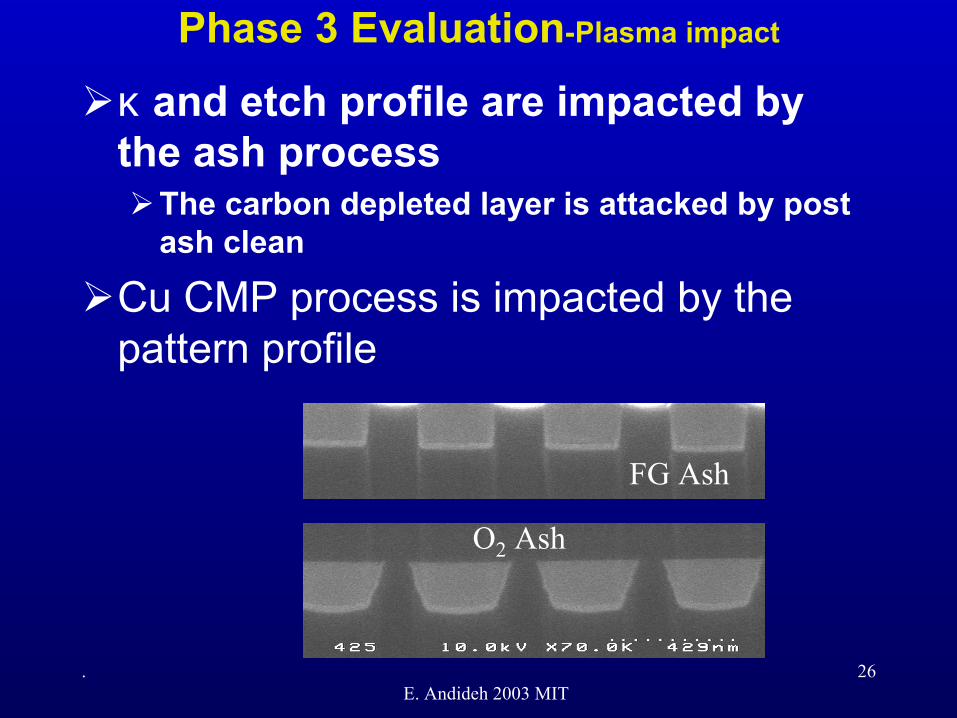
Phase 3 Evaluation-Plasma impact
κ and etch profile are impacted by the ash process
The carbon depleted layer is attacked by post ash clean
Cu CMP process is impacted by the pattern profile
FG Ash
O2 Ash
.E. Andideh 2003 MIT
27
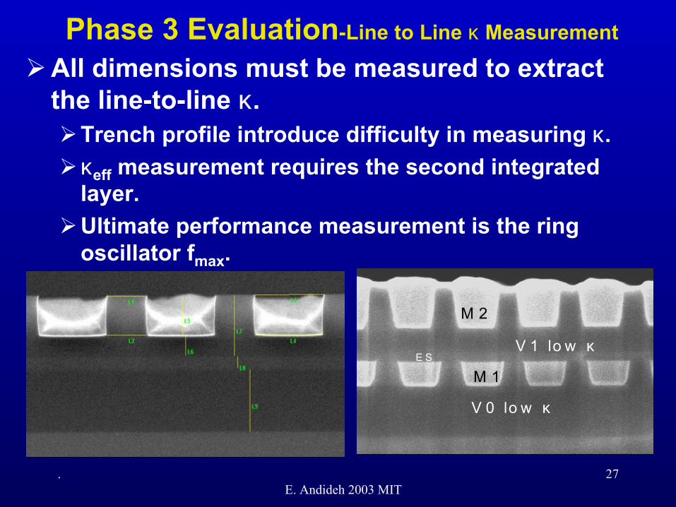
All dimensions must be measured to extract the line-to-line κ.
Trench profile introduce difficulty in measuring κ.κeff measurement requires the second integrated layer.Ultimate performance measurement is the ring oscillator fmax.
Phase 3 Evaluation-Line to Line κ Measurement
M 1
M 2
V 1 lo w κ
V 0 lo w κ
E S
M 1
M 2
V 1 lo w κ
V 0 lo w κ
M 1
M 2
V 1 lo w κ
V 0 lo w κ
E S
.E. Andideh 2003 MIT
28
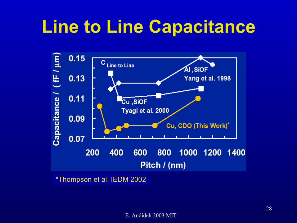
Line to Line Capacitance
*Thompson et al. IEDM 2002
*
.E. Andideh 2003 MIT
29
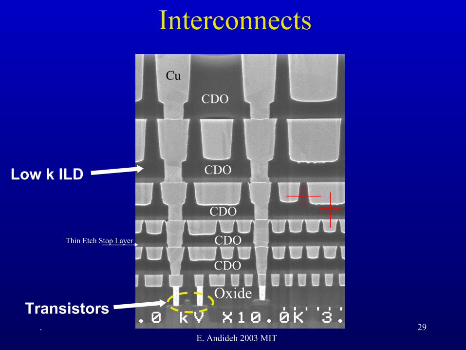
Interconnects
Thin Etch Stop Layer
CDO
CDO
Oxide
CDO
CDO
CDO
Cu
Transistors
Low k ILD
.E. Andideh 2003 MIT
30
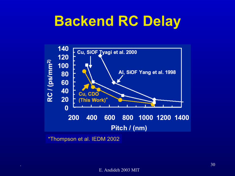
Backend RC Delay
*Thompson et al. IEDM 2002
*
.E. Andideh 2003 MIT
31
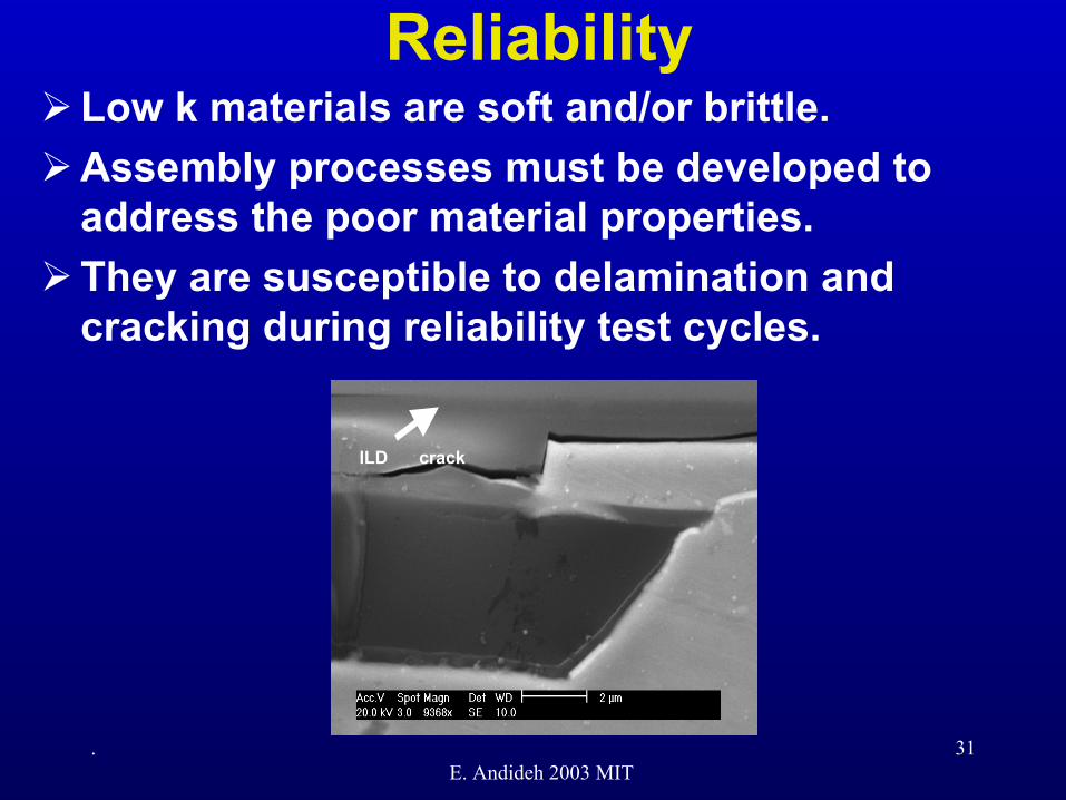
ILD crack
ReliabilityLow k materials are soft and/or brittle.Assembly processes must be developed to address the poor material properties.They are susceptible to delamination and cracking during reliability test cycles.
.E. Andideh 2003 MIT
32
ConclusionsInterconnect engineers face many challenges in evaluating and integrating new materials.
It is important to screen out new materials and focus resources on minimum number of potential candidates.
A methodology has been outlined to evaluate the new material efficiently and effectively.
We have successfully integrated CVD CDO low κILD film in 90 nm technology.
Use of CVD CDO low k ILD can reduce LtL capacitance >20% compared to SiOF.
.E. Andideh 2003 MIT
33
Acknowledgements
. Author wish to thank Mark Bohr, Chi-Hwa Tsang, Chia-Hong Jan, Ajay Jain, Loren Chow, Huey-Chiang Liou, Mansour Moinpour, Jessica Xu, Jun He, Ying Zhou and Markus Kuhn for their technical advice and support.
.E. Andideh 2003 MIT
34
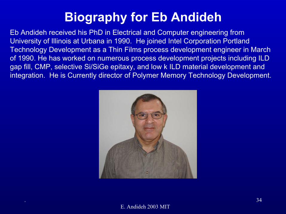
Biography for Eb AndidehEb Andideh received his PhD in Electrical and Computer engineering from University of Illinois at Urbana in 1990. He joined Intel Corporation Portland Technology Development as a Thin Films process development engineer in March of 1990. He has worked on numerous process development projects including ILD gap fill, CMP, selective Si/SiGe epitaxy, and low k ILD material development and integration. He is Currently director of Polymer Memory Technology Development.