EUV Lithography - eng.kuleuven.be · 2D multi patterning LE = Litho –Etch Critical overlay =...
26
EUV Lithography Coming to your local IC manufacturer! Soon TM Arenberg Youngster Seminar – May 16, 2018 Vu Luong, PhD STUDENT
Transcript of EUV Lithography - eng.kuleuven.be · 2D multi patterning LE = Litho –Etch Critical overlay =...
EUV LithographyComing to your local IC manufacturer! SoonTM
Arenberg Youngster Seminar – May 16, 2018
Vu Luong, PhD STUDENT
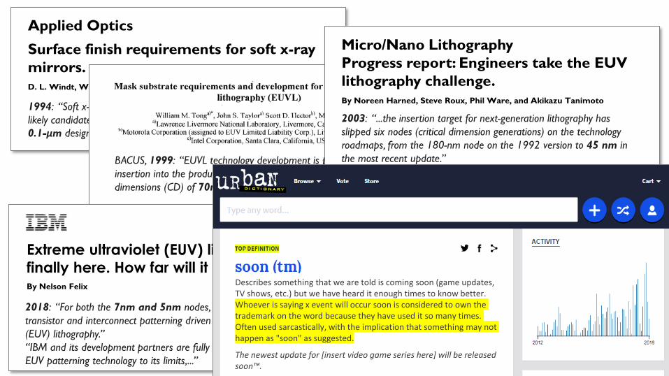
1994: “Soft x-ray projection lithography (SXPL) is considered to be a
likely candidate for the mass production of integrated circuits having
0.1-μm design rules”
Applied Optics
Surface finish requirements for soft x-ray
mirrors.
D. L. Windt, W. K. Waskiewicz, and J. E. Griffith
BACUS, 1999: “EUVL technology development is progressing toward
insertion into the production of integrated circuits with critical
dimensions (CD) of 70nm. ”
2003: “...the insertion target for next-generation lithography has
slipped six nodes (critical dimension generations) on the technology
roadmaps, from the 180-nm node on the 1992 version to 45 nm in
the most recent update.”
Micro/Nano Lithography
Progress report: Engineers take the EUV
lithography challenge.
By Noreen Harned, Steve Roux, Phil Ware, and Akikazu Tanimoto
2014: “It’s the worst kept secret in the industry, but extreme
ultraviolet (EUV) lithography will likely miss the 10nm node.”
What If EUV Fails?By Mark Lapedus
2018: “For both the 7nm and 5nm nodes, IBM... relied heavily on
transistor and interconnect patterning driven by Extreme Ultraviolet
(EUV) lithography.”
“IBM and its development partners are fully committed to extending
EUV patterning technology to its limits,...”
Extreme ultraviolet (EUV) lithography is
finally here. How far will it go?By Nelson Felix
Describes something that we are told is coming soon (game updates, TV shows, etc.) but we have heard it enough times to know better. Whoever is saying x event will occur soon is considered to own the trademark on the word because they have used it so many times. Often used sarcastically, with the implication that something may not happen as "soon" as suggested.
The newest update for [insert video game series here] will be released soon™.
PUBLIC
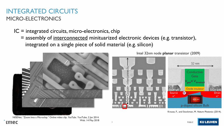
INTEGRATED CIRCUITS
IC = integrated circuits, micro-electronics, chip
= assembly of interconnected minituarized electronic devices (e.g. transistor),
integrated on a single piece of solid material (e.g. silicon)
3
MICRO-ELECTRONICS
NISENet. “Zoom Into a Microchip.” Online video clip. YouTube. YouTube, 2 Jan 2014.
Web. 14 May 2018
Krausz, F., and Stockman, M. Nature Photonics (2014).
Intel 32nm node planar transistor (2009)
Conductive
Gate
Oxide insulator
Source
n+
p-doped silicon Bulk
e- Drain
n+
Vgate< VthresholdVgate> Vthreshold
PUBLIC
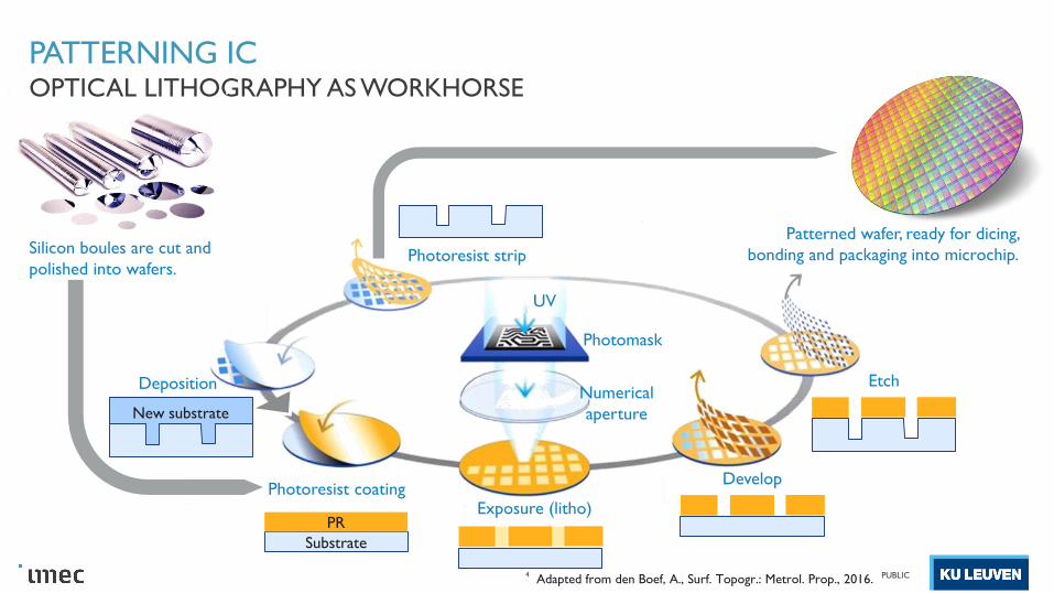
Develop
PATTERNING IC
4
OPTICAL LITHOGRAPHY AS WORKHORSE
Silicon boules are cut and
polished into wafers.
UV
Photomask
Numerical
aperture
Exposure (litho)
Etch
Photoresist strip
Photoresist coating
Substrate
PR
Patterned wafer, ready for dicing,
bonding and packaging into microchip.
Deposition
New substrate
Adapted from den Boef, A., Surf. Topogr.: Metrol. Prop., 2016.
PUBLIC
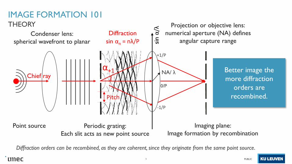
IMAGE FORMATION 101
5
THEORY
Point source Periodic grating:
Each slit acts as new point source
Condenser lens:
spherical wavefront to planar
Diffraction
Pitch
sin αn = nλ/P
α+1
Projection or objective lens:
numerical aperture (NA) defines
angular capture range
Imaging plane:
Image formation by recombination
+1st order
0th order
-1st order
sin α
/λ
+1/P
0/P
-1/P
NA/ λChief ray
Better image the
more diffraction
orders are
recombined.
Diffraction orders can be recombined, as they are coherent, since they originate from the same point source.
PUBLIC
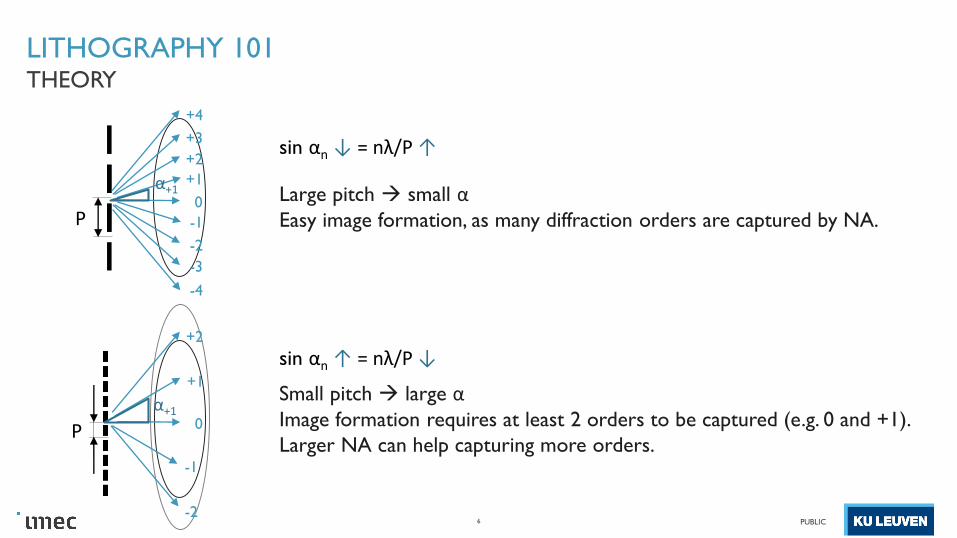
LITHOGRAPHY 101
6
THEORY
Large pitch small αEasy image formation, as many diffraction orders are captured by NA.
sin αn ↓ = nλ/P ↑
P
P
+4
+3
+2
+1
0
-1
-2
-3
-4
α+1
+2
+1
0
-1
-2
α+1Small pitch large αImage formation requires at least 2 orders to be captured (e.g. 0 and +1).
Larger NA can help capturing more orders.
sin αn ↑ = nλ/P ↓
PUBLIC
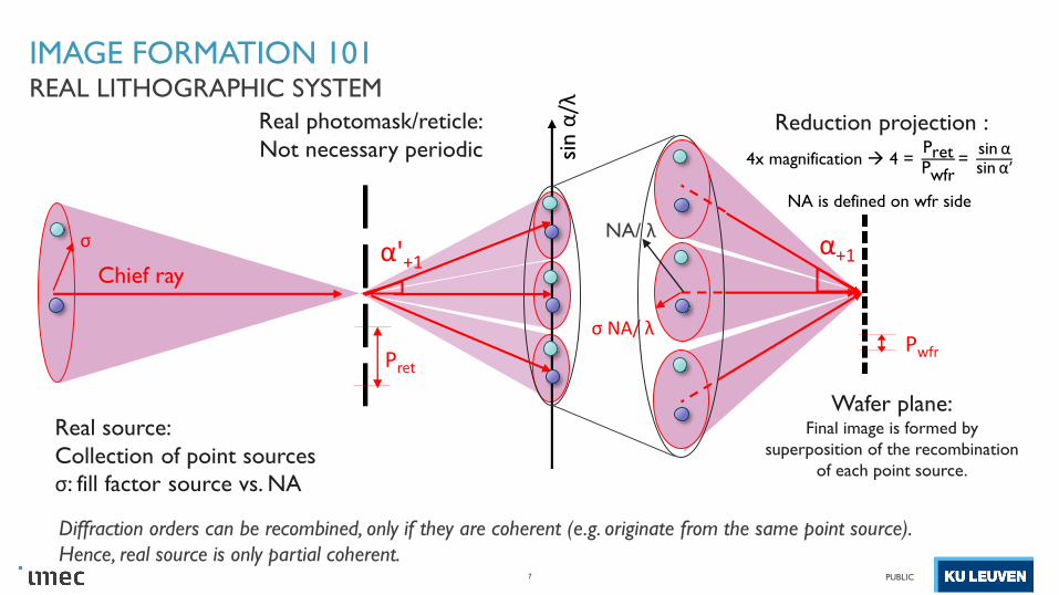
IMAGE FORMATION 101
7
REAL LITHOGRAPHIC SYSTEM
Real source:
Collection of point sources
σ: fill factor source vs. NA
Chief ray
Diffraction orders can be recombined, only if they are coherent (e.g. originate from the same point source).
Hence, real source is only partial coherent.
σ
Real photomask/reticle:
Not necessary periodic
Pret
α'+1
sin α
/λ
σ NA/ λ
α+1
Pwfr
Reduction projection :
4x magnification 4 =PretPwfr
=sin αsin α′
NA is defined on wfr side
NA/ λ
Wafer plane:Final image is formed by
superposition of the recombination
of each point source.
PUBLIC
IMAGE FORMATION 101
8
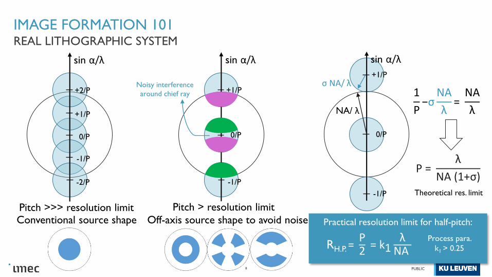
REAL LITHOGRAPHIC SYSTEM
sin α/λ
+2/P
+1/P
0/P
-1/P
-2/P
Pitch >>> resolution limitConventional source shape
sin α/λ
+1/P
-1/P
0/P
Pitch > resolution limit
Off-axis source shape to avoid noise
Noisy interference
around chief ray
Practical resolution limit for half-pitch:
RH.P. =P2 = k1
λNA
sin α/λ
+1/P
-1/P
0/P
σ NA/ λ
NA/ λ
1
P−σ
NA
λ=NA
λ
P =λ
NA (1+σ)Theoretical res. limit
Process para.
k1 > 0.25
9
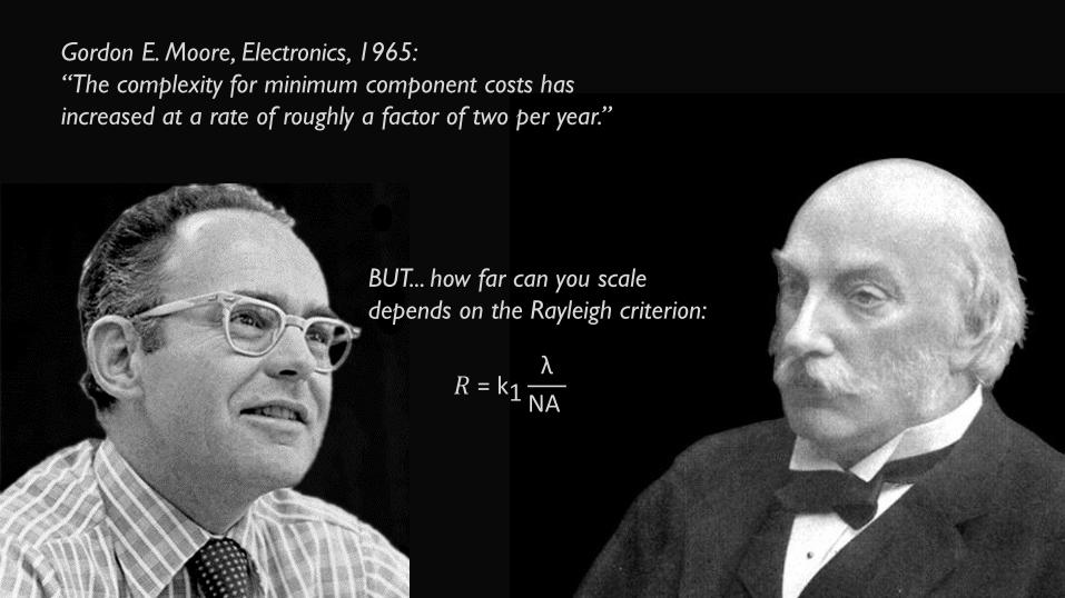
Gordon E. Moore, Electronics, 1965:
“The complexity for minimum component costs has
increased at a rate of roughly a factor of two per year.”
BUT... how far can you scale
depends on the Rayleigh criterion:
𝑅 = k1λ
NA
PUBLIC
TECHNOLOGY NODE
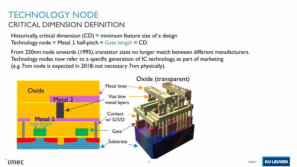
Historically, critical dimension (CD) = minimum feature size of a design
Technology node = Metal 1 half-pitch = Gate length = CD
From 250nm node onwards (1995), transistor sizes no longer match between different manufacturers.
Technology nodes now refer to a specific generation of IC technology, as part of marketing
(e.g. 7nm node is expected in 2018; not necessary 7nm physically).
CRITICAL DIMENSION DEFINITION
10
Gate
Contact
w/ G/S/D
Metal lines
Substrate
Vias btw
metal layers
Oxide
Oxide (transparent)
Metal 2
Metal 1Gate length
PUBLIC
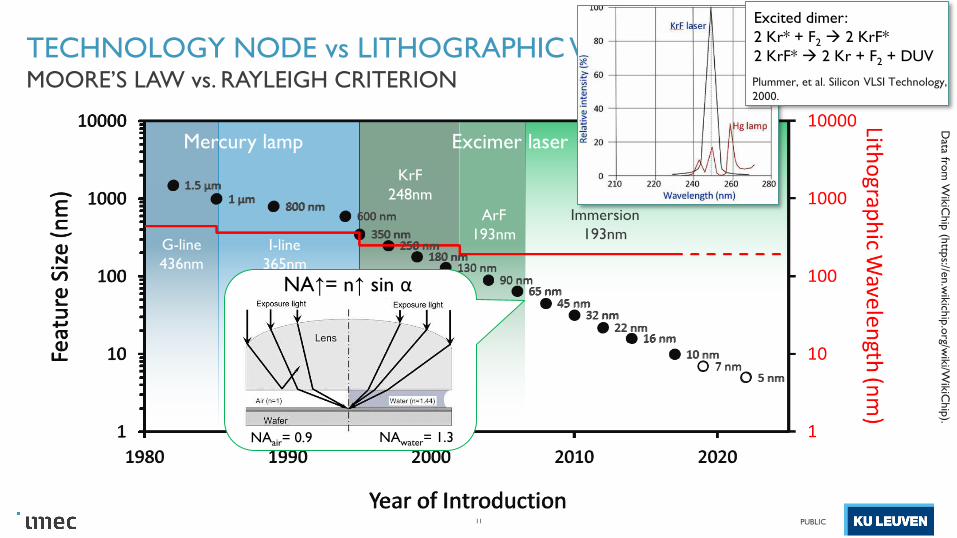
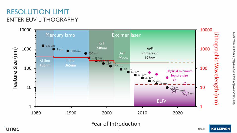
G-line
436nm
Mercury lamp
I-line
365nm
Excimer laser
KrF
248nm
ArF
193nm
Immersion
193nm
Data fro
m W
ikiC
hip
(http
s://en.w
ikich
ip.o
rg/wik
i/Wik
iChip
).
TECHNOLOGY NODE vs LITHOGRAPHIC WAVELENGTH
11
MOORE’S LAW vs. RAYLEIGH CRITERION
Excited dimer:
2 Kr* + F2 2 KrF*
2 KrF* 2 Kr + F2 + DUV
Plummer, et al. Silicon VLSI Technology,
2000.
NAwater= 1.3 NAair= 0.9
NA↑= n↑ sin α
PUBLIC
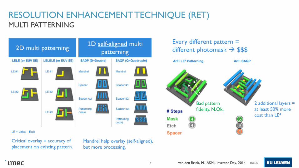
RESOLUTION ENHANCEMENT TECHNIQUE (RET)
12
MULTI PATTERNING
van den Brink, M., ASML Investor Day, 2014.
2D multi patterning
LE = Litho – Etch
Critical overlay = accuracy of
placement on existing pattern.
1D self-aligned multi
patterning
Every different pattern =
different photomask $$$
Bad pattern
fidelity. N.Ok.
2 additional layers =
at least 50% more
cost than LE4
Mandrel help overlay (self-aligned),
but more processing.
PUBLIC
EUV
13
G-line
436nm
Mercury lamp
I-line
365nm
Excimer laser
KrF
248nm
ArF
193nm
Immersion
193nm
RESOLUTION LIMITENTER EUV LITHOGRAPHY
Data fro
m W
ikiC
hip
(http
s://en.w
ikich
ip.o
rg/wik
i/Wik
iChip
).
Physical minimum
feature size
ArFi
PUBLIC
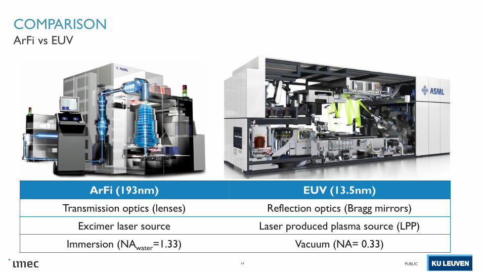
COMPARISON
14
ArFi vs EUV
ArFi (193nm) EUV (13.5nm)
Transmission optics (lenses) Reflection optics (Bragg mirrors)
Excimer laser source Laser produced plasma source (LPP)
Immersion (NAwater=1.33) Vacuum (NA= 0.33)
PUBLIC
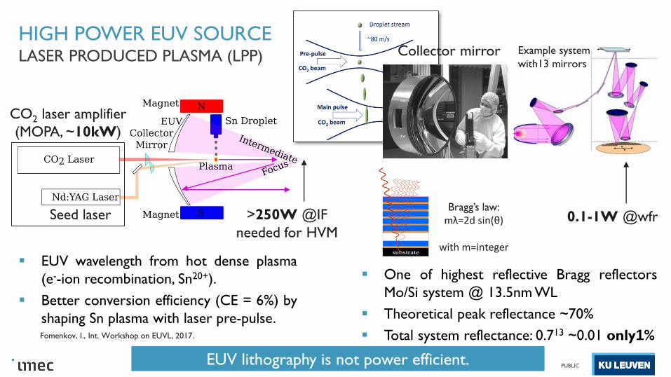
HIGH POWER EUV SOURCE
15
LASER PRODUCED PLASMA (LPP)
▪ EUV wavelength from hot dense plasma
(e--ion recombination, Sn20+).
▪ Better conversion efficiency (CE = 6%) by
shaping Sn plasma with laser pre-pulse.
CO2 laser amplifier
(MOPA, ~10kW)
Seed laser >250W @IF
needed for HVM
EUV lithography is not power efficient.
Bragg’s law:
mλ=2d sin(θ)
with m=integer
▪ One of highest reflective Bragg reflectors
Mo/Si system @ 13.5nm WL
▪ Theoretical peak reflectance ~70%
▪ Total system reflectance: 0.713 ~0.01 only1%
Collector mirror Example system
with13 mirrors
0.1-1W @wfr
Fomenkov, I., Int. Workshop on EUVL, 2017.
PUBLIC
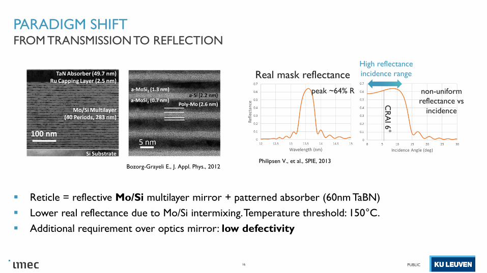
Real mask reflectance
Philipsen V., et al., SPIE, 2013
peak ~64% R non-uniform
reflectance vs
incidence
CR
AI 6
°
PARADIGM SHIFT
▪ Reticle = reflective Mo/Si multilayer mirror + patterned absorber (60nm TaBN)
▪ Lower real reflectance due to Mo/Si intermixing. Temperature threshold: 150°C.
▪ Additional requirement over optics mirror: low defectivity
16
FROM TRANSMISSION TO REFLECTION
Bozorg-Grayeli E., J. Appl. Phys., 2012
High reflectance
incidence range
PUBLIC
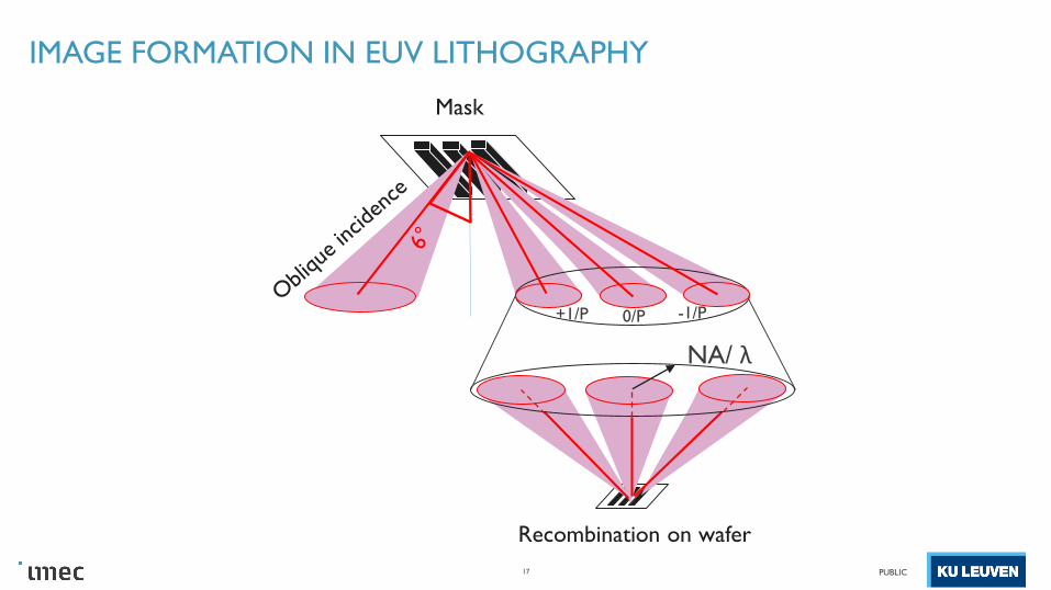
Mask
IMAGE FORMATION IN EUV LITHOGRAPHY
17
Recombination on wafer
NA/ λ
+1/P 0/P -1/P
PUBLIC
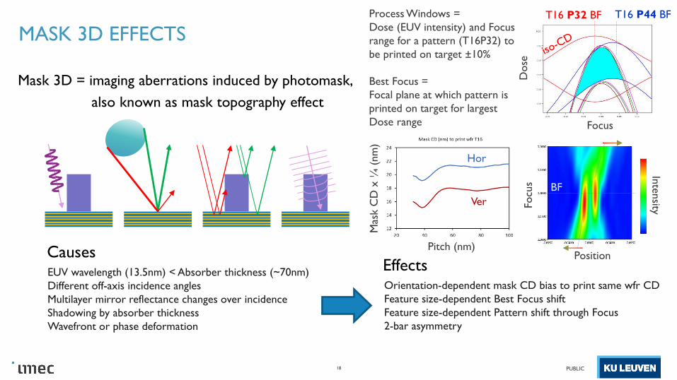
MASK 3D EFFECTS
Mask 3D = imaging aberrations induced by photomask,
also known as mask topography effect
18
EUV wavelength (13.5nm) < Absorber thickness (~70nm)
Different off-axis incidence angles
Multilayer mirror reflectance changes over incidence
Shadowing by absorber thickness
Wavefront or phase deformation
CausesEffectsOrientation-dependent mask CD bias to print same wfr CD
Feature size-dependent Best Focus shift
Feature size-dependent Pattern shift through Focus
2-bar asymmetry
Focus
Dose
T16 P32 BF T16 P44 BF
Hor
Ver
Mas
k C
D x
¼ (
nm
)
Pitch (nm)
Process Windows =
Dose (EUV intensity) and Focus
range for a pattern (T16P32) to
be printed on target ±10%
Best Focus =
Focal plane at which pattern is
printed on target for largest
Dose range
Focu
s
Position
Inte
nsity
BF
PUBLIC
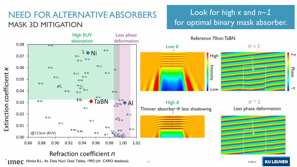
NEED FOR ALTERNATIVE ABSORBERS
19
MASK 3D MITIGATION
High EUV
absorption
Less phase
deformation
High κThinner absorber less shadowing
n ~ 1Less phase deformation
High
Low In
tensity
Low κ n < 1
+π
-π
Reference 70nm TaBN
Phase
Look for high κ and n~1
for optimal binary mask absorber.
@13.5nm (EUV)
Henke B.L., At. Data Nucl. Data Tables, 1993 (cfr. CXRO database).
PUBLIC
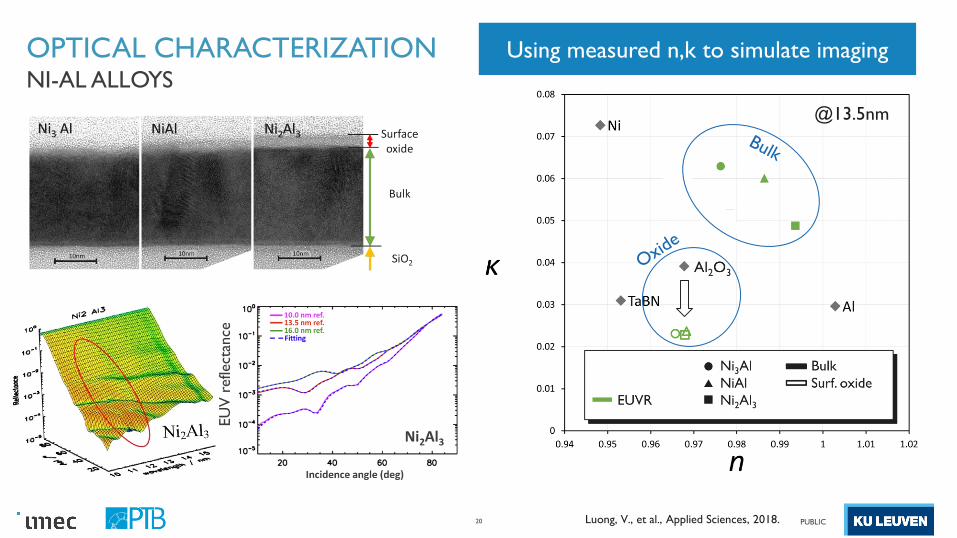
OPTICAL CHARACTERIZATIONNI-AL ALLOYS
EU
V r
eflect
ance
20 Luong, V., et al., Applied Sciences, 2018.
@13.5nm
Using measured n,k to simulate imaging
PUBLIC
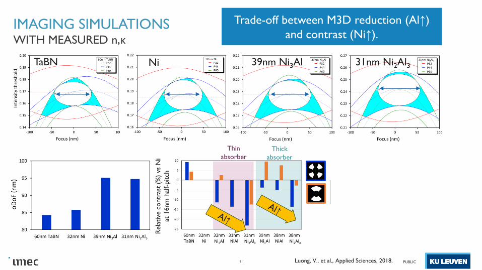
IMAGING SIMULATIONS
21
WITH MEASURED n,κ
TaBN Ni 39nm Ni3Al 31nm Ni2Al3
Trade-off between M3D reduction (Al↑)
and contrast (Ni↑).
Rela
tive
co
ntr
ast
(%)
vs N
i
at 1
6nm
hal
f-pitch
Thin
absorberThick
absorber
Luong, V., et al., Applied Sciences, 2018.
PUBLIC
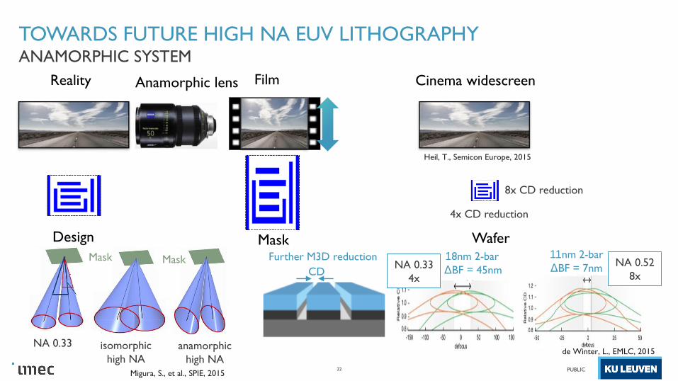
TOWARDS FUTURE HIGH NA EUV LITHOGRAPHY
22
ANAMORPHIC SYSTEM
Reality Film Cinema widescreenNormal lensAnamorphic lens
Design Mask Wafer
4x CD reduction
8x CD reduction
NA 0.33 isomorphic
high NA
anamorphic
high NA
Migura, S., et al., SPIE, 2015
NA 0.33
4x
NA 0.52
8xCD
18nm 2-bar 11nm 2-barFurther M3D reduction
ΔBF = 45nm ΔBF = 7nm
de Winter, L., EMLC, 2015
Heil, T., Semicon Europe, 2015
Mask Mask
PUBLIC
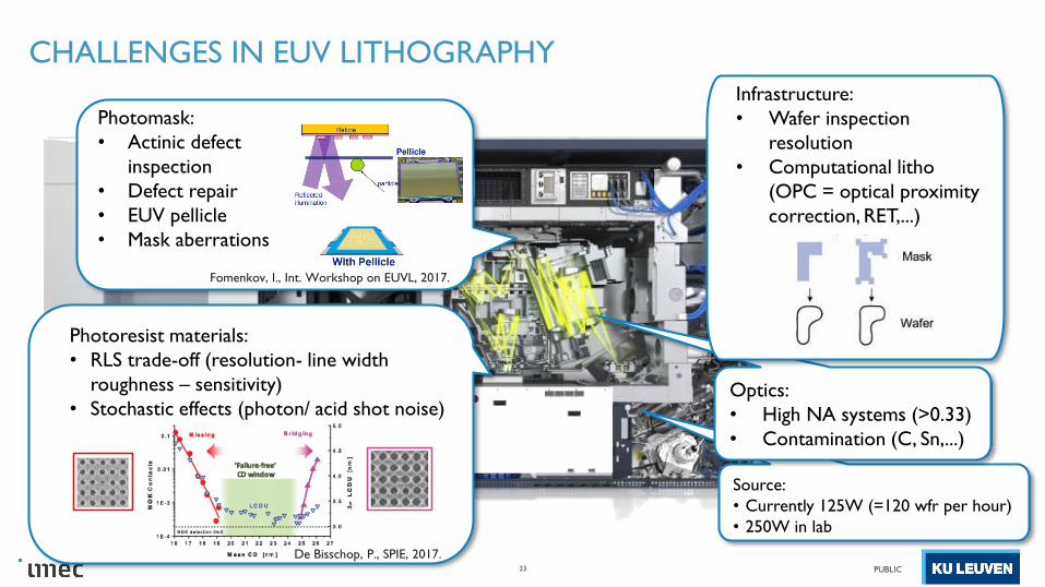
CHALLENGES IN EUV LITHOGRAPHY
23
Source:
• Currently 125W (=120 wfr per hour)
• 250W in lab
Optics:
• High NA systems (>0.33)
• Contamination (C, Sn,...)
Photoresist materials:
• RLS trade-off (resolution- line width
roughness – sensitivity)
• Stochastic effects (photon/ acid shot noise)
De Bisschop, P., SPIE, 2017.
Photomask:
• Actinic defect
inspection
• Defect repair
• EUV pellicle
• Mask aberrations
Fomenkov, I., Int. Workshop on EUVL, 2017.
Infrastructure:
• Wafer inspection
resolution
• Computational litho
(OPC = optical proximity
correction, RET,...)
PUBLIC
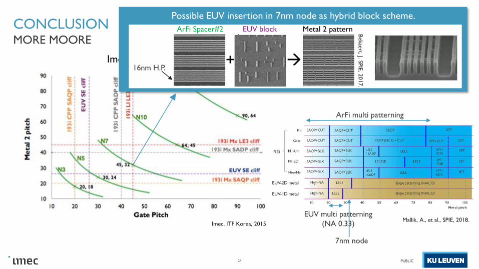
Imec logic roadmap
CONCLUSION
24
MORE MOORE
Imec, ITF Korea, 2015
ArFi multi patterning
7nm node
EUV multi patterning
(NA 0.33)Mallik, A., et al., SPIE, 2018.
Possible EUV insertion in 7nm node as hybrid block scheme.
Bekae
rt, J. SPIE
, 2017.
ArFi Spacer#2 EUV block Metal 2 pattern
+ 16nm H.P.
PUBLIC
Scaling enabled by EUV (NA 0.33)
and new design
Scaling enabled by high NA EUV
and new systems
w/o EUV (NA 0.33)
w/o high NA EUV
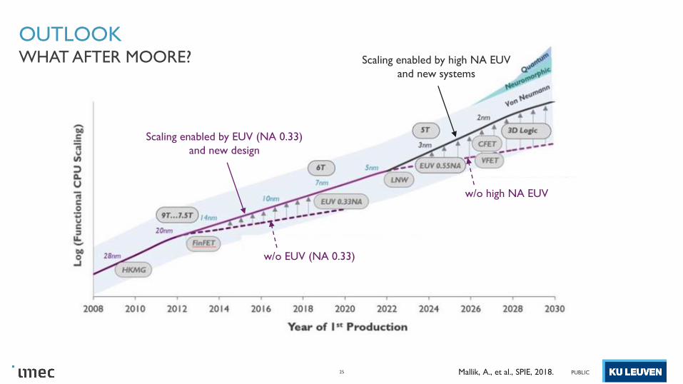
OUTLOOK
25
WHAT AFTER MOORE?
Mallik, A., et al., SPIE, 2018.

PUBLIC26
Thanks for your attention!