Electronic properties of graphene - I
38
Electronic properties of graphene - I Vladimir Falko helped by V.Cheianov, E.McCann K.Kechedzhi, D.Abergel T.Ando, B.Altshuler, I.Aleiner
Transcript of Electronic properties of graphene - I
Electronic properties of graphene - I
Vladimir Falko
helped byV.Cheianov, E.McCannK.Kechedzhi, D.Abergel
T.Ando, B.Altshuler, I.Aleiner
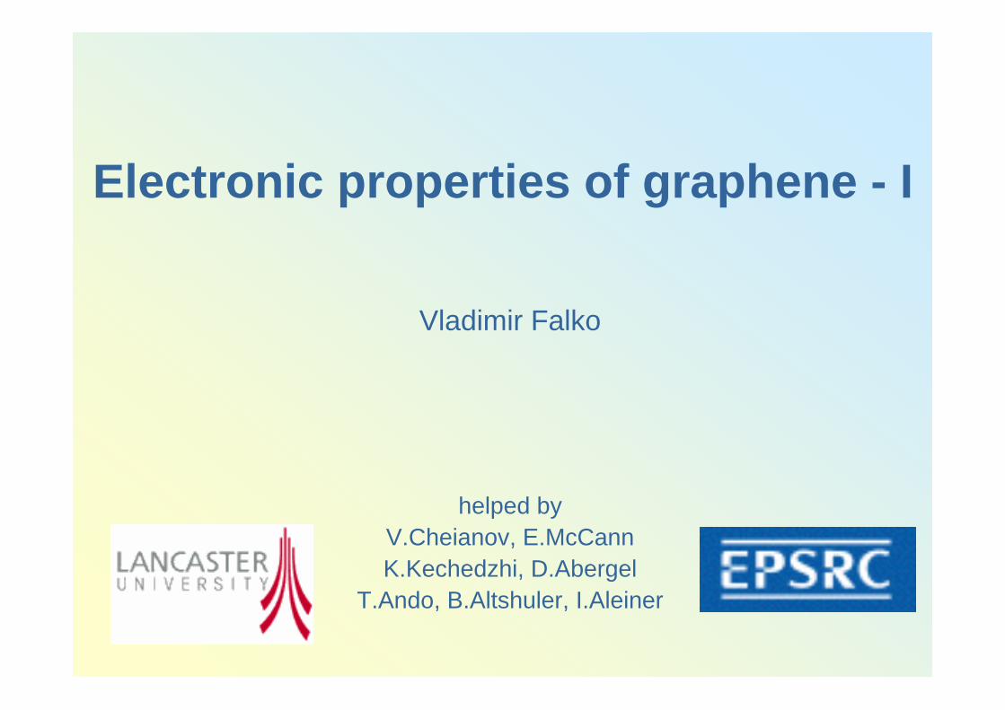
Ultra-thin graphitic films: from flakes to micro-devices
for references, see the review articleGeim and Novoselov - Nature Mat. 6, 183 (2007)
Novoselov et al -Science 306, 666 (2004)
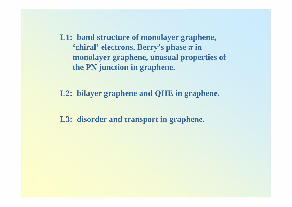
L1: band structure of monolayer graphene, ‘chiral’ electrons, Berry’s phase π in monolayer graphene, unusual properties of the PN junction in graphene.
L2: bilayer graphene and QHE in graphene.
L3: disorder and transport in graphene.
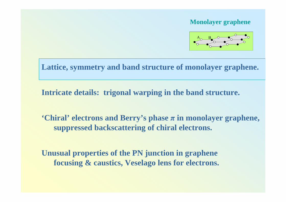
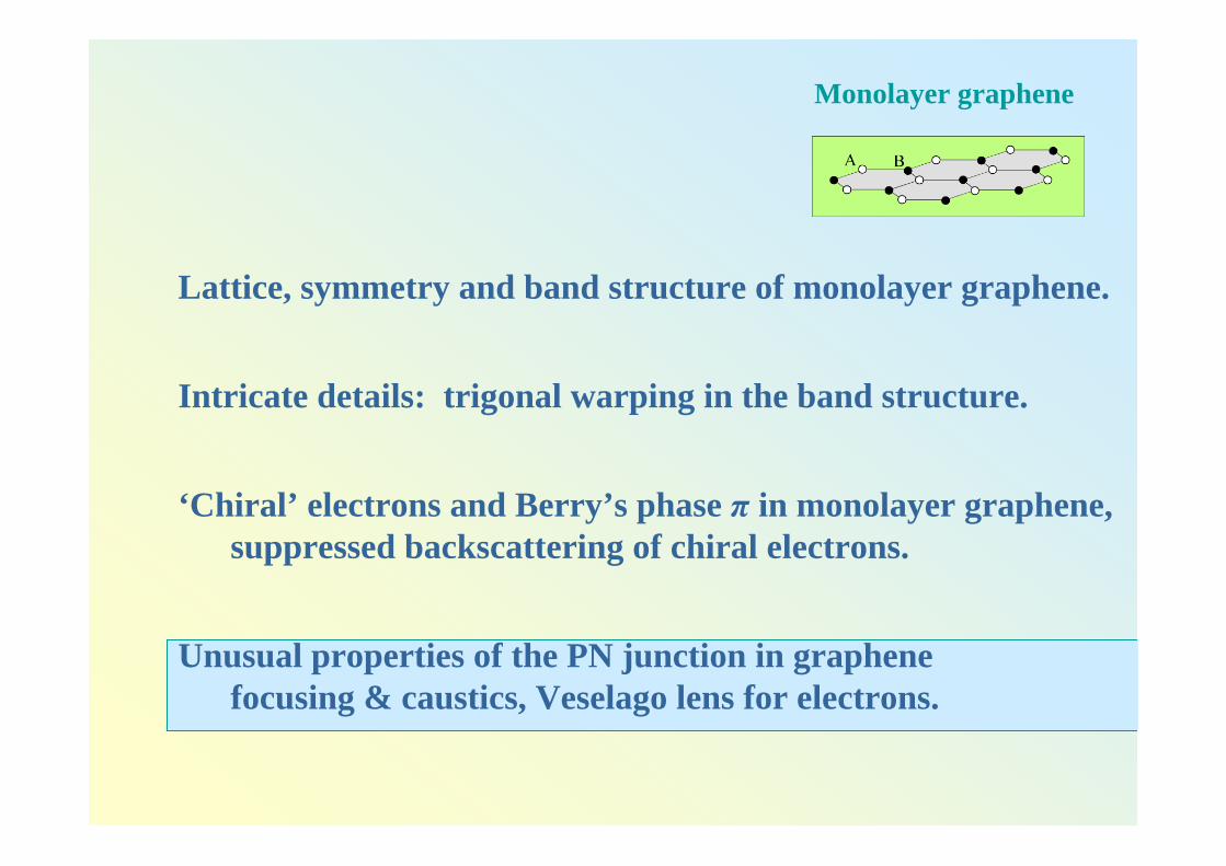
Monolayer graphene
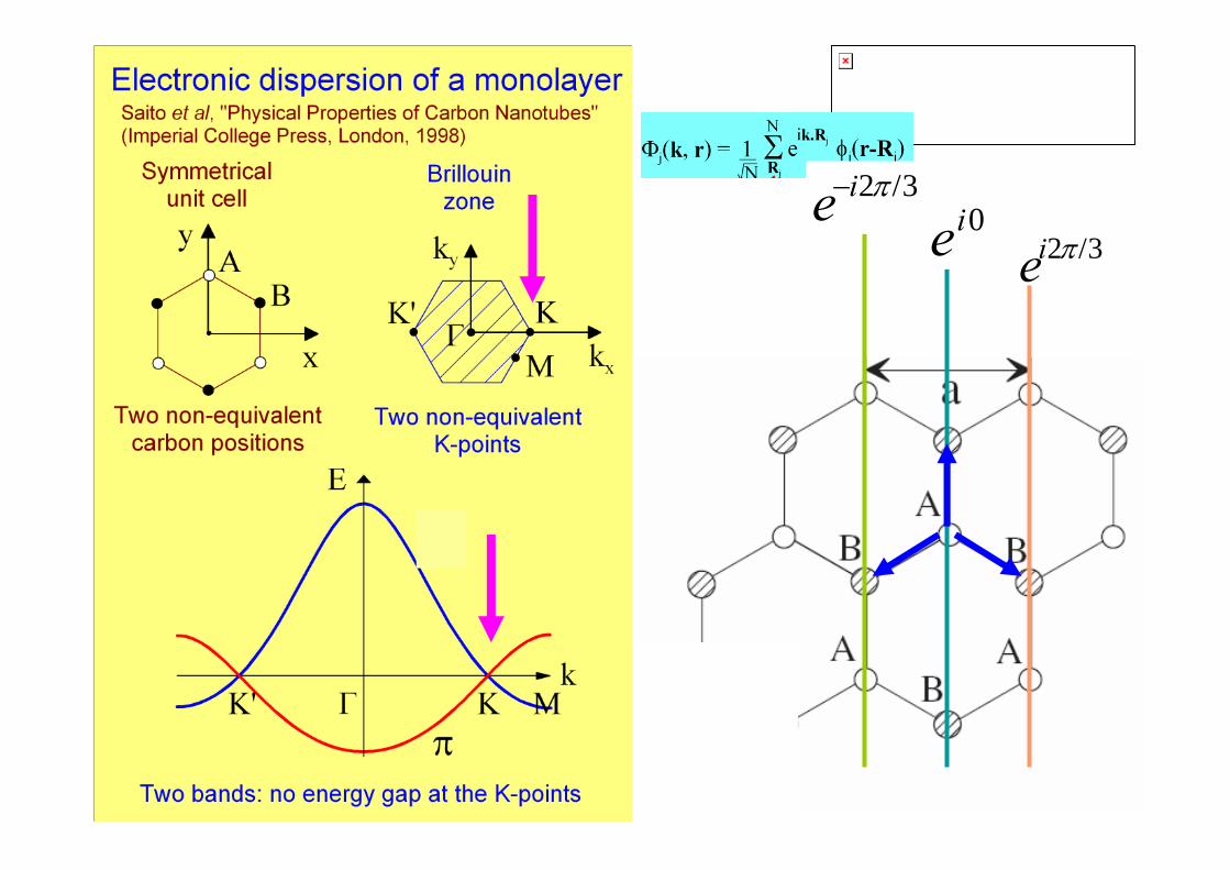
Lattice, symmetry and band structure of monolayer graphene.
Intricate details: trigonal warping in the band structure.
‘Chiral’ electrons and Berry’s phase π in monolayer graphene, suppressed backscattering of chiral electrons.
Unusual properties of the PN junction in graphene focusing & caustics, Veselago lens for electrons.
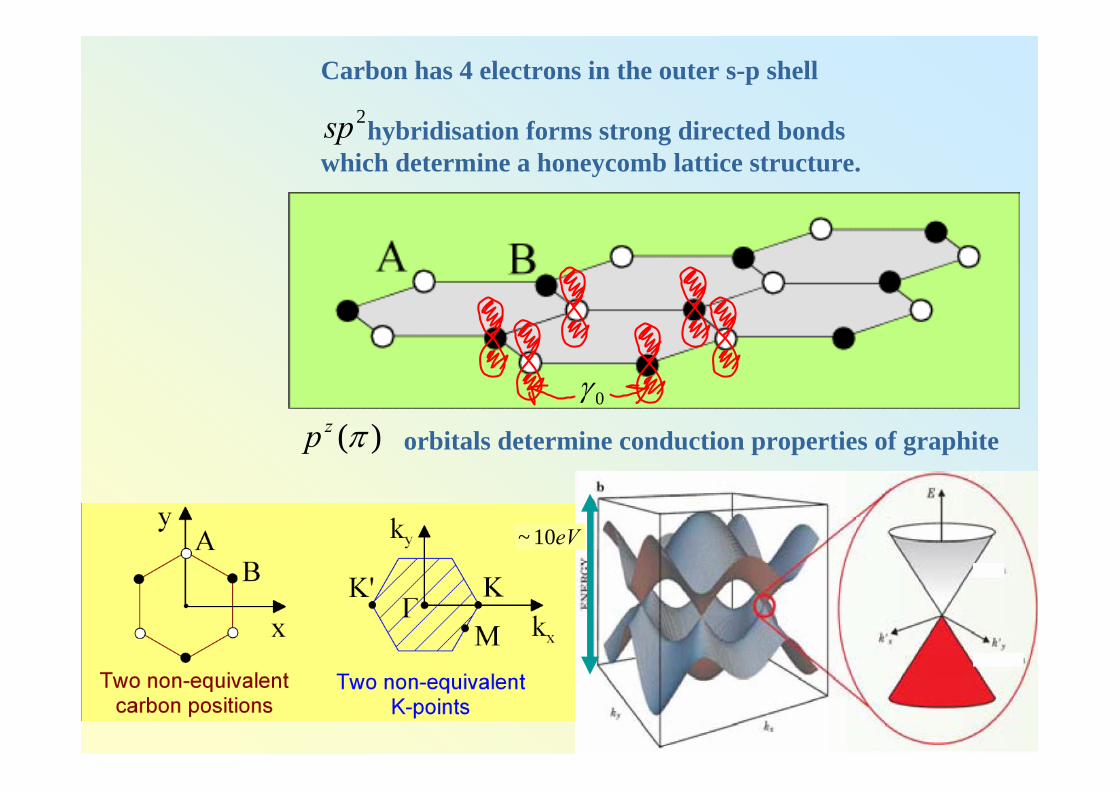
σ - bonds
hybridisation forms strong directed bonds which determine a honeycomb lattice structure.
2sp
C
Carbon has 4 electrons in the outer s-p shell
)(πzp orbitals determine conduction properties of graphite
0γ
eV10~
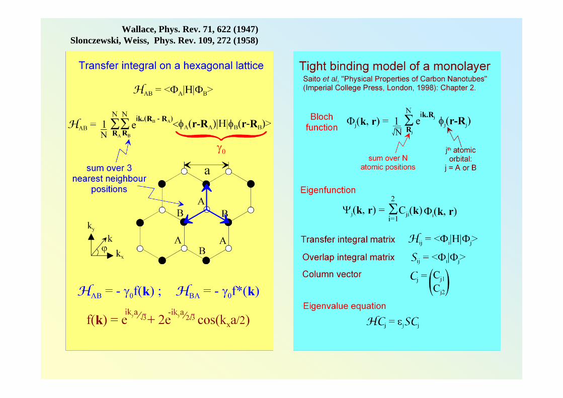
Wallace, Phys. Rev. 71, 622 (1947)Slonczewski, Weiss, Phys. Rev. 109, 272 (1958)
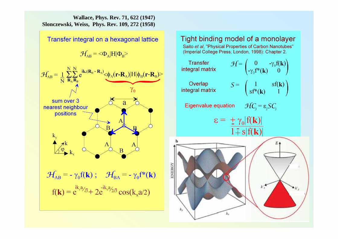
Wallace, Phys. Rev. 71, 622 (1947)Slonczewski, Weiss, Phys. Rev. 109, 272 (1958)
0ie 3/2πiepr
3/2πie−
0ie 3/2πie
3/2πie−
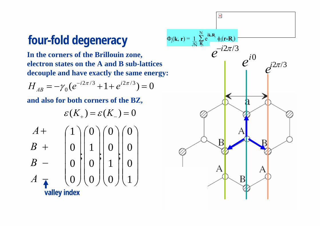
0)()( == −+ KK εε
⎟⎟⎟⎟⎟
⎠
⎞
⎜⎜⎜⎜⎜
⎝
⎛
⎟⎟⎟⎟⎟
⎠
⎞
⎜⎜⎜⎜⎜
⎝
⎛
⎟⎟⎟⎟⎟
⎠
⎞
⎜⎜⎜⎜⎜
⎝
⎛
⎟⎟⎟⎟⎟
⎠
⎞
⎜⎜⎜⎜⎜
⎝
⎛
−−++
1000
;
0100
;
0010
;
0001
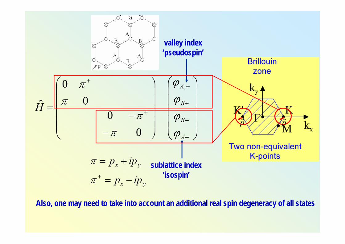
ABBA
valley index
In the corners of the Brillouin zone, electron states on the A and B sub-lattices decouple and have exactly the same energy:
and also for both corners of the BZ,
0)1( 3/23/20 =++−= − ππγ ii
AB eeH
four-fold degeneracy
⎟⎟⎟⎟⎟
⎠
⎞
⎜⎜⎜⎜⎜
⎝
⎛
⎟⎟⎟⎟⎟
⎠
⎞
⎜⎜⎜⎜⎜
⎝
⎛
⎟⎟⎟⎟⎟
⎠
⎞
⎜⎜⎜⎜⎜
⎝
⎛
⎟⎟⎟⎟⎟
⎠
⎞
⎜⎜⎜⎜⎜
⎝
⎛
−−++
1000
;
0100
;
0010
;
0001
ABBA
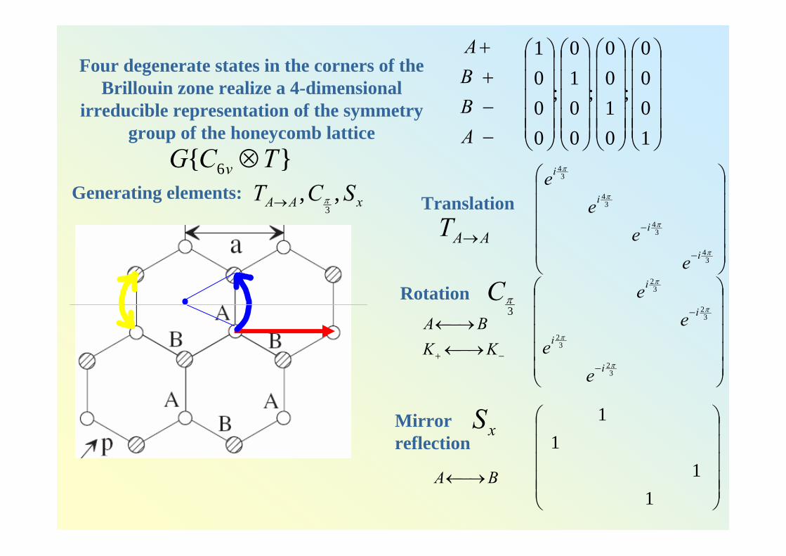
Four degenerate states in the corners of the Brillouin zone realize a 4-dimensional
irreducible representation of the symmetry group of the honeycomb lattice
Translation
AAT →⎟⎟⎟⎟⎟
⎠
⎞
⎜⎜⎜⎜⎜
⎝
⎛
−
−
34
34
34
34
π
π
π
π
i
i
i
i
ee
ee
Generating elements: xAA SCT ,,3π→
3πCRotation
⎟⎟⎟⎟⎟
⎠
⎞
⎜⎜⎜⎜⎜
⎝
⎛
−
−
32
32
32
32
π
π
π
π
i
i
i
i
ee
ee
−+ ⎯→←⎯→←
KKBA
Mirror reflection
xS
⎟⎟⎟⎟⎟
⎠
⎞
⎜⎜⎜⎜⎜
⎝
⎛
11
11
BA ⎯→←
}{ 6 TCG v ⊗
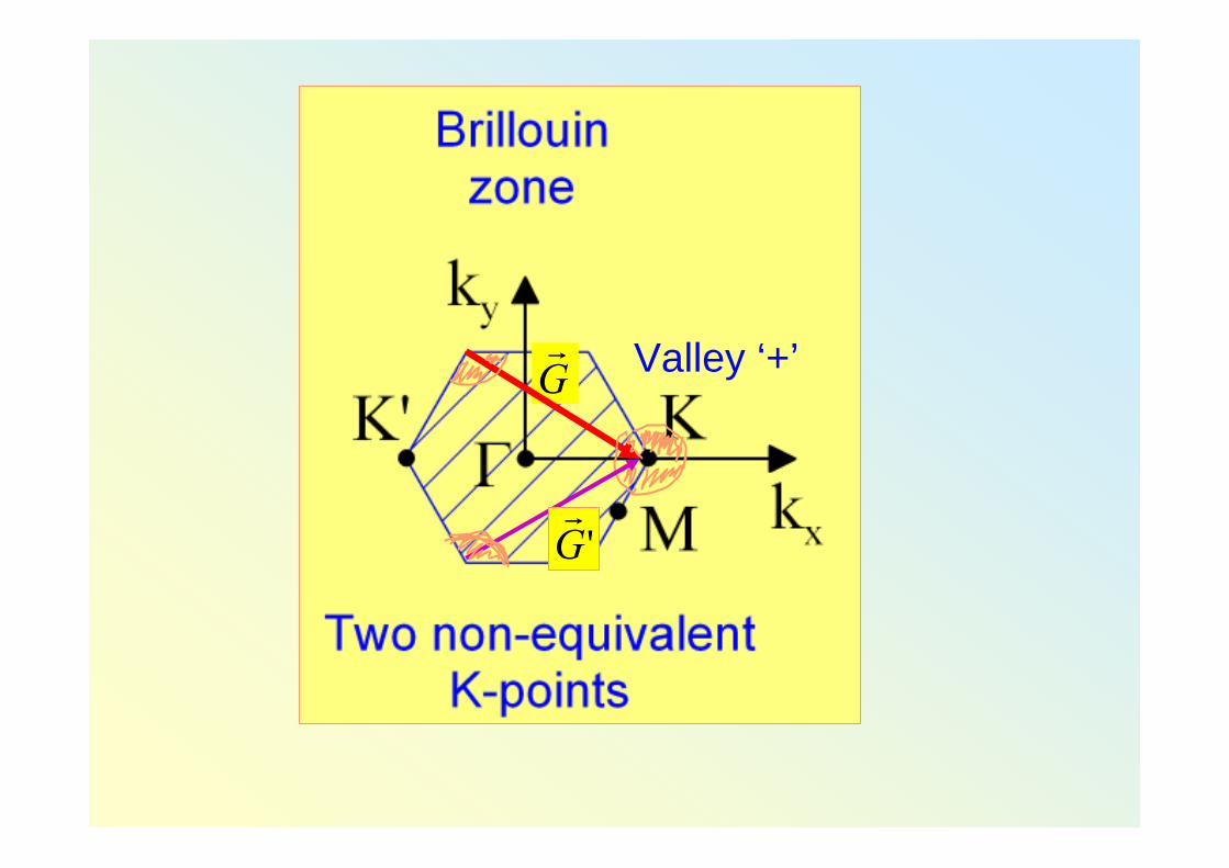
Gr
'Gr
Valley ‘+’
pr
(valleys)
pK rr++pK rr
+−
⎥⎦⎤
⎢⎣⎡ ++−=
−+−−
+
)()(0,
32232
332232 y
ax
ay
ay
ax
a ppiipippiiKAB eeeeeH
ππ
γ
sec8
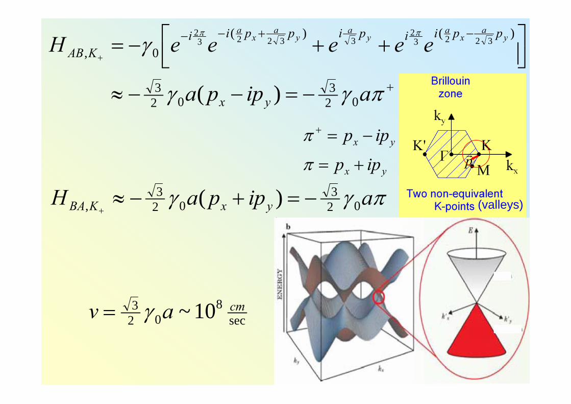
023 10~ cmav γ=
πγγ aippaH yxKBA 023
023
, )( −=+−≈+
+−=−−≈ πγγ aippa yx 023
023 )(
yx
yx
ipp
ipp
+=
−=+
π
π
⎟⎟⎟⎟⎟
⎠
⎞
⎜⎜⎜⎜⎜
⎝
⎛
⎟⎟⎟⎟⎟
⎠
⎞
⎜⎜⎜⎜⎜
⎝
⎛
−−
=
−
−
+
+
+
+
A
B
B
A
H
ϕϕϕϕ
ππ
ππ ,
00
00
ˆ
valley index‘pseudospin’
sublattice index‘isospin’
yx
yx
ipp
ipp
−=
+=+π
π
Also, one may need to take into account an additional real spin degeneracy of all states
prpr
π+π
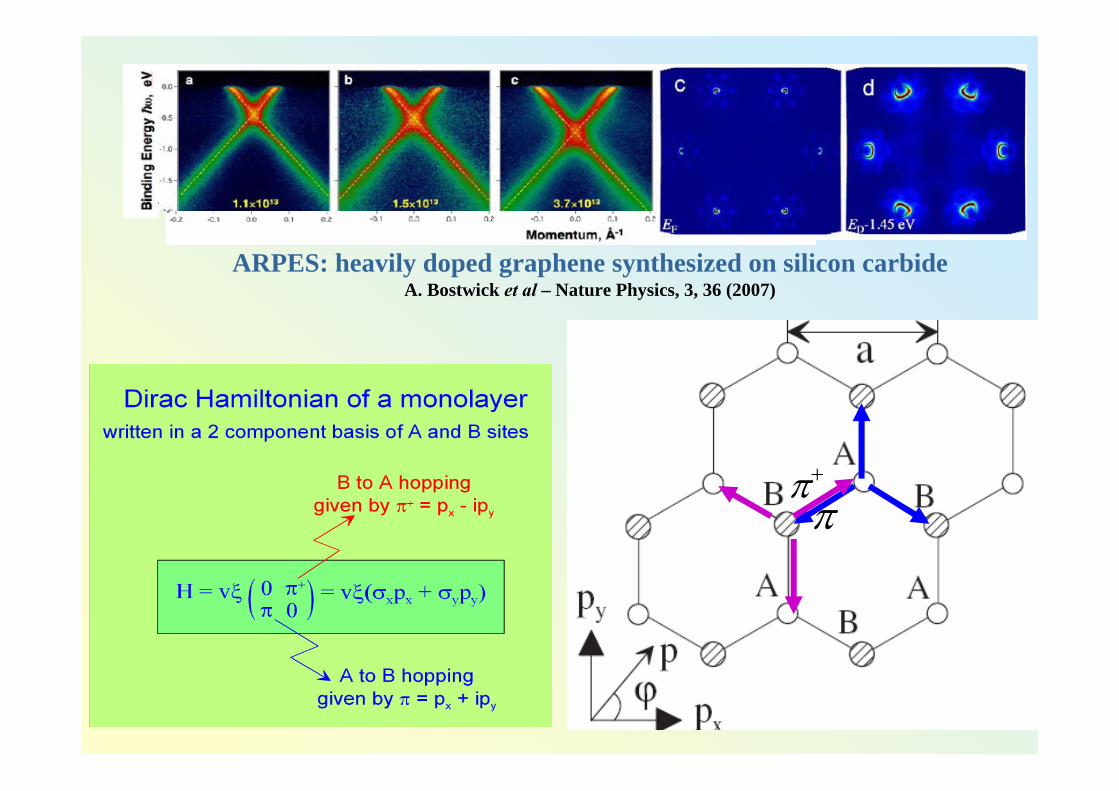
ARPES: heavily doped graphene synthesized on silicon carbideA. Bostwick et al – Nature Physics, 3, 36 (2007)
Monolayer graphene
Lattice, symmetry and band structure of monolayer graphene.
Intricate details: trigonal warping in the band structure.
‘Chiral’ electrons and Berry’s phase π in monolayer graphene, suppressed backscattering of chiral electrons.
Unusual properties of the PN junction in graphene focusing & caustics, Veselago lens for electrons.
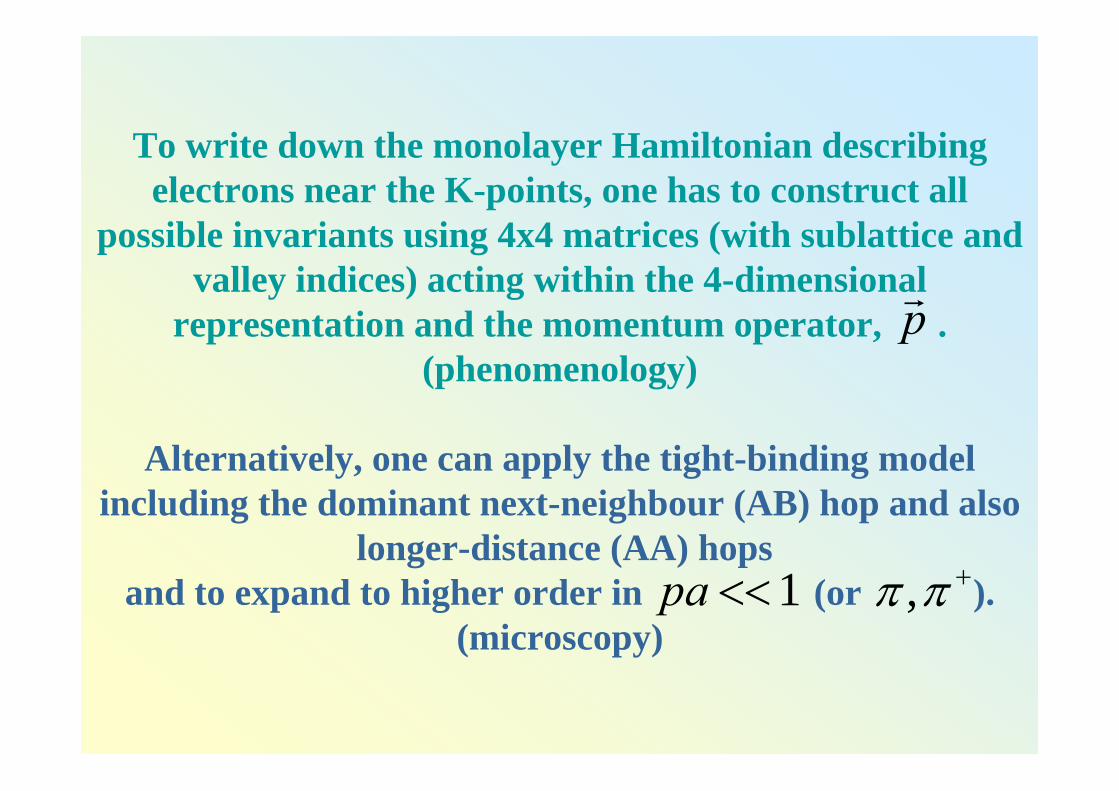
To write down the monolayer Hamiltonian describing electrons near the K-points, one has to construct all
possible invariants using 4x4 matrices (with sublattice and valley indices) acting within the 4-dimensional
representation and the momentum operator, . (phenomenology)
Alternatively, one can apply the tight-binding model including the dominant next-neighbour (AB) hop and also
longer-distance (AA) hops and to expand to higher order in (or ).
(microscopy)
pr
1<<pa +ππ ,
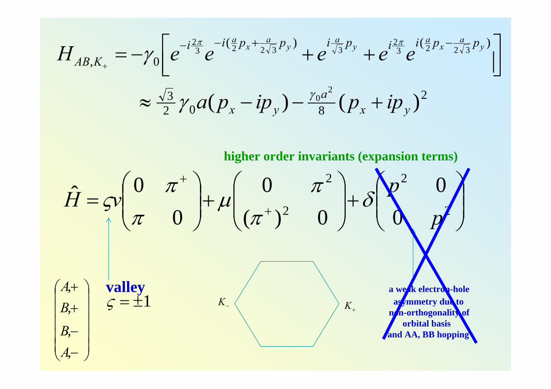
higher order invariants (expansion terms)
valley a weak electron-hole asymmetry due to
non-orthogonality oforbital basis
and AA, BB hopping⎟⎟⎟⎟⎟
⎠
⎞
⎜⎜⎜⎜⎜
⎝
⎛
−−
++
,,,,
ABBA
⎟⎟⎠
⎞⎜⎜⎝
⎛+⎟⎟⎠
⎞⎜⎜⎝
⎛+⎟⎟⎠
⎞⎜⎜⎝
⎛=
+
+
2
2
2
2
00
0)(0
00ˆ
pp
vH δπ
πμ
ππ
ς
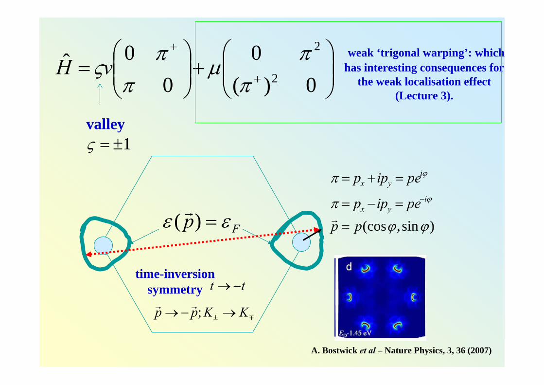
1±=ς+K−K
⎥⎦⎤
⎢⎣⎡ ++−=
−+−−
+
)()(0,
32232
332232 y
ax
ay
ay
ax
a ppiipippiiKAB eeeeeH
ππ
γ
2802
3 )()(2
0yx
ayx ippippa +−−≈ γγ
valley
⎟⎟⎠
⎞⎜⎜⎝
⎛+⎟⎟⎠
⎞⎜⎜⎝
⎛=
+
+
0)(0
00ˆ
2
2
ππ
μπ
πςvH
1±=ς
Fp εε =)( rϕ
ϕ
π
πi
yx
iyx
peipp
peipp−=−=
=+=
)sin,(cos ϕϕpp =r
A. Bostwick et al – Nature Physics, 3, 36 (2007)
weak ‘trigonal warping’: which has interesting consequences for
the weak localisation effect (Lecture 3).
m
rr KKpp
tt
→−→
−→
±;
time-inversionsymmetry
Monolayer graphene
Lattice, symmetry and band structure of monolayer graphene.
Intricate details: trigonal warping in the band structure.
‘Chiral’ electrons and Berry’s phase π in monolayer graphene, suppressed backscattering of chiral electrons.
Unusual properties of the PN junction in graphene focusing & caustics, Veselago lens for electrons.
Monolayer
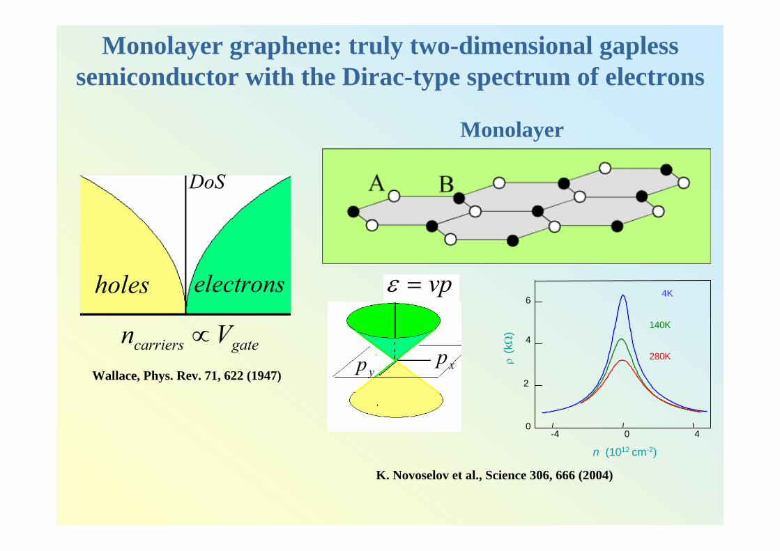
Monolayer graphene: truly two-dimensional gapless semiconductor with the Dirac-type spectrum of electrons
DoS
gatecarriers Vn ∝
holes electrons vp=|| ε
xpyp2
4
0
ρ(kΩ
)
6
4-4 0
n (1012 cm-2)
280K
4K
140K
K. Novoselov et al., Science 306, 666 (2004)
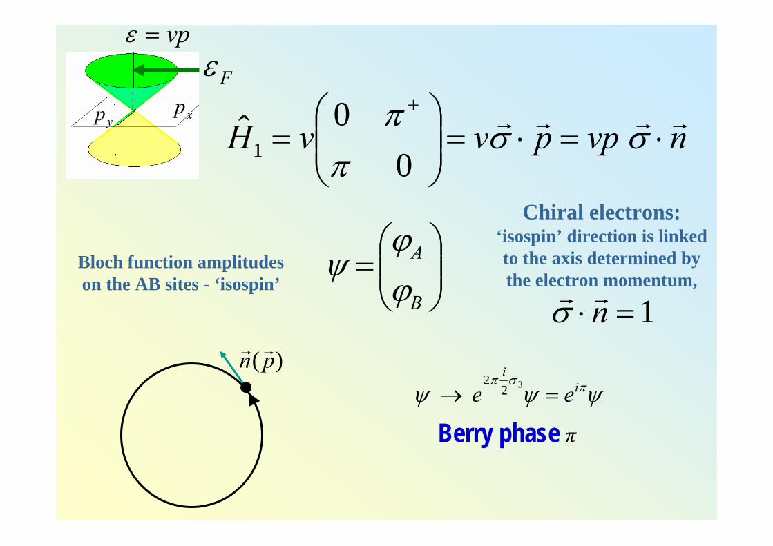
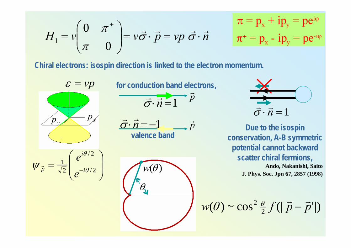
vp=ε
xpypWallace, Phys. Rev. 71, 622 (1947)
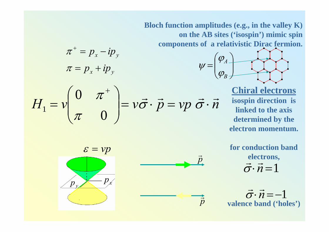
nvppvvH rrrr⋅=⋅=⎟⎟
⎠
⎞⎜⎜⎝
⎛=
+
σσπ
π0
01
Bloch function amplitudes (e.g., in the valley K) on the AB sites (‘isospin’) mimic spin
components of a relativistic Dirac fermion.
⎟⎟⎠
⎞⎜⎜⎝
⎛=
B
A
ϕϕ
ψ
vp=ε
xpyp
Chiral electronsisospin direction is linked to the axis
determined by the electron momentum.
for conduction band electrons,
valence band (‘holes’)
1=⋅nrrσ
1−=⋅nrrσ
pr
pr
yx
yx
ipp
ipp
+=
−=+
π
π
nvppvvH rrrr⋅=⋅=⎟⎟
⎠
⎞⎜⎜⎝
⎛=
+
σσπ
π0
0ˆ1
)( pn rr
Berry phase πψψψ πσπ i
i
ee =→32
2
Chiral electrons:‘isospin’ direction is linked to the axis determined by the electron momentum,
Bloch function amplitudes on the AB sites - ‘isospin’ ⎟⎟
⎠
⎞⎜⎜⎝
⎛=
B
A
ϕϕ
ψ1=⋅nrrσ
vp=ε
xpyp
Fε
nvppvvH rrrr⋅=⋅=⎟⎟
⎠
⎞⎜⎜⎝
⎛=
+
σσπ
π0
01
vp=ε
xpyp
Chiral electrons: isospin direction is linked to the electron momentum.
for conduction band electrons,
valence band
1=⋅nrrσ
1−=⋅nrrσ
pr
pr Due to the isospinconservation, A-B symmetric
potential cannot backward scatter chiral fermions,
Ando, Nakanishi, Saito J. Phys. Soc. Jpn 67, 2857 (1998)
1=⋅nrrσ
|)'(|cos~)( 22 ppfw rr
−θθ
θ
)(θw⎟⎟⎠
⎞⎜⎜⎝
⎛=
− 2/
2/
21
θ
θ
ψ i
i
p ee
r
Monolayer graphene
Lattice, symmetry and band structure of monolayer graphene.
Intricate details: trigonal warping in the band structure.
‘Chiral’ electrons and Berry’s phase π in monolayer graphene, suppressed backscattering of chiral electrons.
Unusual properties of the PN junction in graphene focusing & caustics, Veselago lens for electrons.
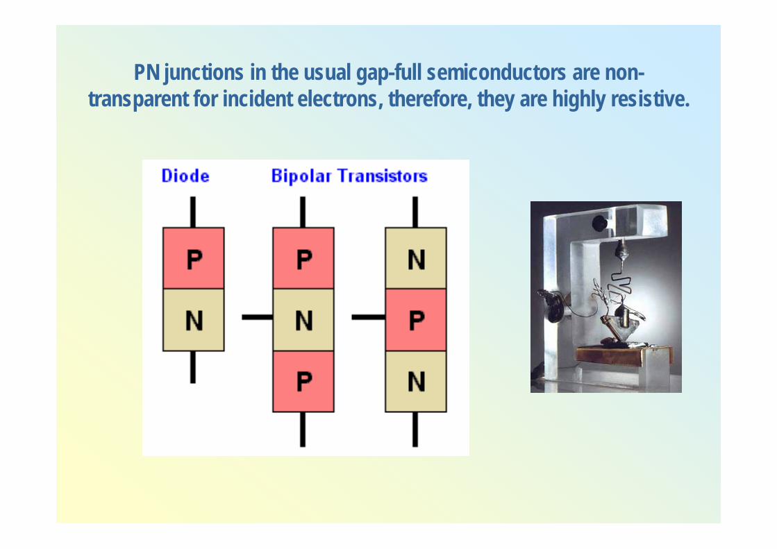
PN junctions in the usual gap-full semiconductors are non-transparent for incident electrons, therefore, they are highly resistive.
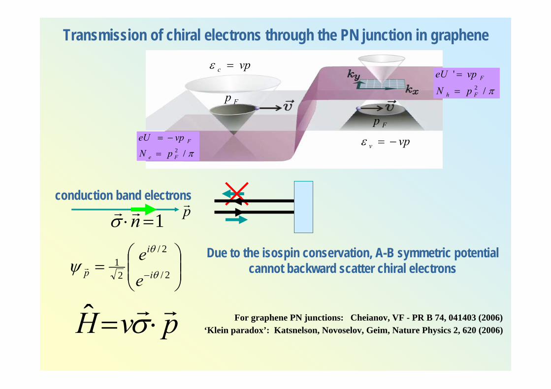
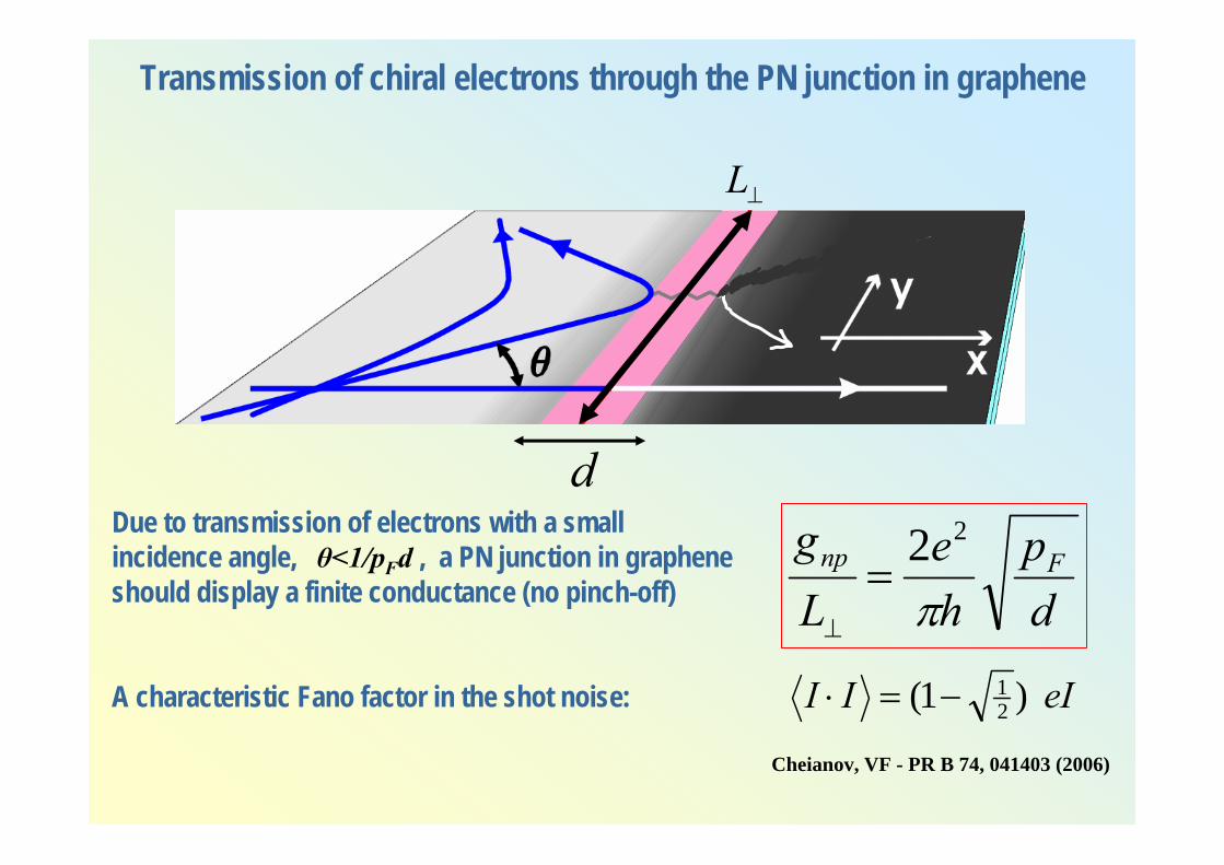
Transmission of chiral electrons through the PN junction in graphene
vpc =ε
vpv −=εFp
Fp
π/2Fe
F
pN
vpeU
=
−=
π/
'2Fh
F
pN
vpeU
=
=
conduction band electrons
1=⋅nrrσ pr
Due to the isospin conservation, A-B symmetric potential cannot backward scatter chiral electrons
For graphene PN junctions: Cheianov, VF - PR B 74, 041403 (2006)‘Klein paradox’: Katsnelson, Novoselov, Geim, Nature Physics 2, 620 (2006)
⎟⎟⎠
⎞⎜⎜⎝
⎛=
− 2/
2/
21
θ
θ
ψ i
i
p ee
r
pvH rr⋅= σˆ
Transmission of chiral electrons through the PN junction in graphene
0=U
⎟⎟⎠
⎞⎜⎜⎝
⎛=
− 2/
2/
21
θ
θ
ψi
i
p ee
r
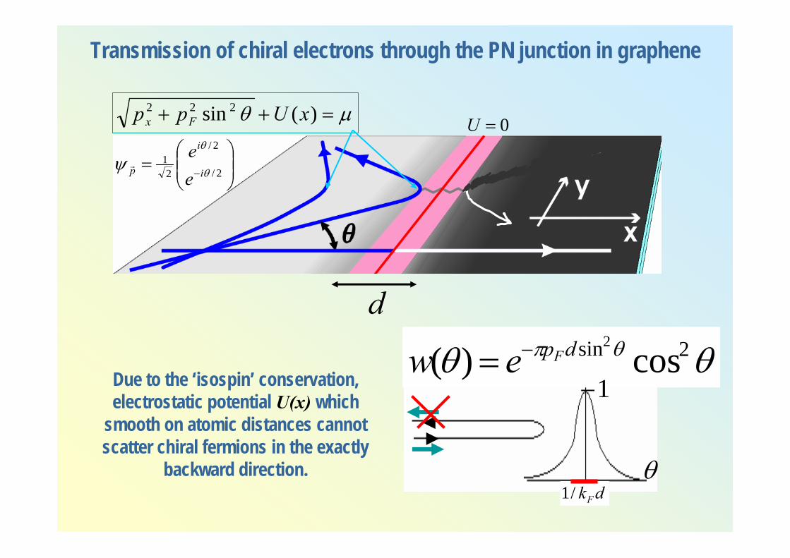
Due to the ‘isospin’ conservation, electrostatic potential U(x) which
smooth on atomic distances cannot scatter chiral fermions in the exactly
backward direction.
θθ θπ 2sin cos)(2dpFew −=
θ
1−
μθ =++ )(sin 222 xUpp Fx
dkF/1
d
dp
he
Lg Fnp
π
22=
⊥
eIII )1( 21−=⋅
Due to transmission of electrons with a small incidence angle, θ<1/pFd , a PN junction in graphene should display a finite conductance (no pinch-off)
A characteristic Fano factor in the shot noise:
Cheianov, VF - PR B 74, 041403 (2006)
Transmission of chiral electrons through the PN junction in graphene
⊥L
d
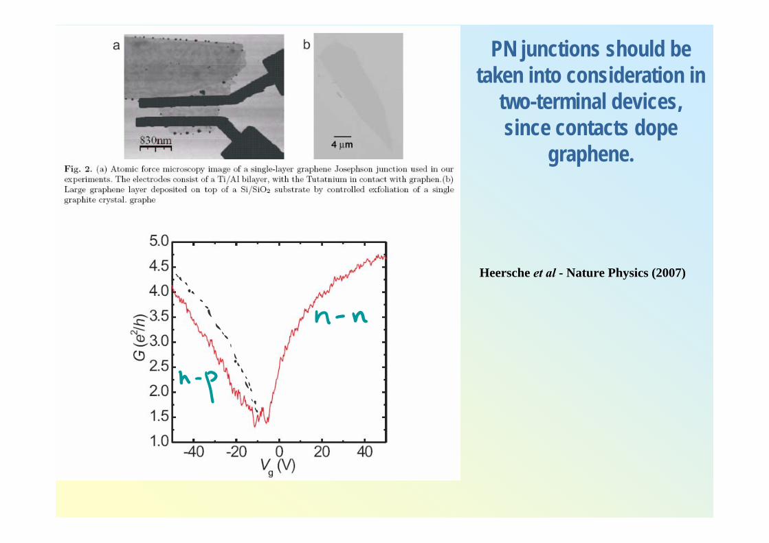
Heersche et al - Nature Physics (2007)
PN junctions should be taken into consideration in
two-terminal devices, since contacts dope
graphene.
ppv
pv
vppcr
rr
r
=∂∂
=
=ε
ε )(
ppv
pv
vppvr
rr
r
−=∂∂
=
−=ε
ε )(
vp
Fermi momentum
cp
Fermi momentum
π/2ce
c
pN
vpeU
=
−=
π/
'2vh
v
pN
vpeU
=
=
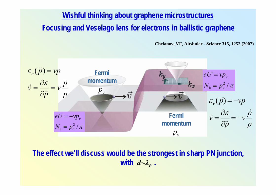
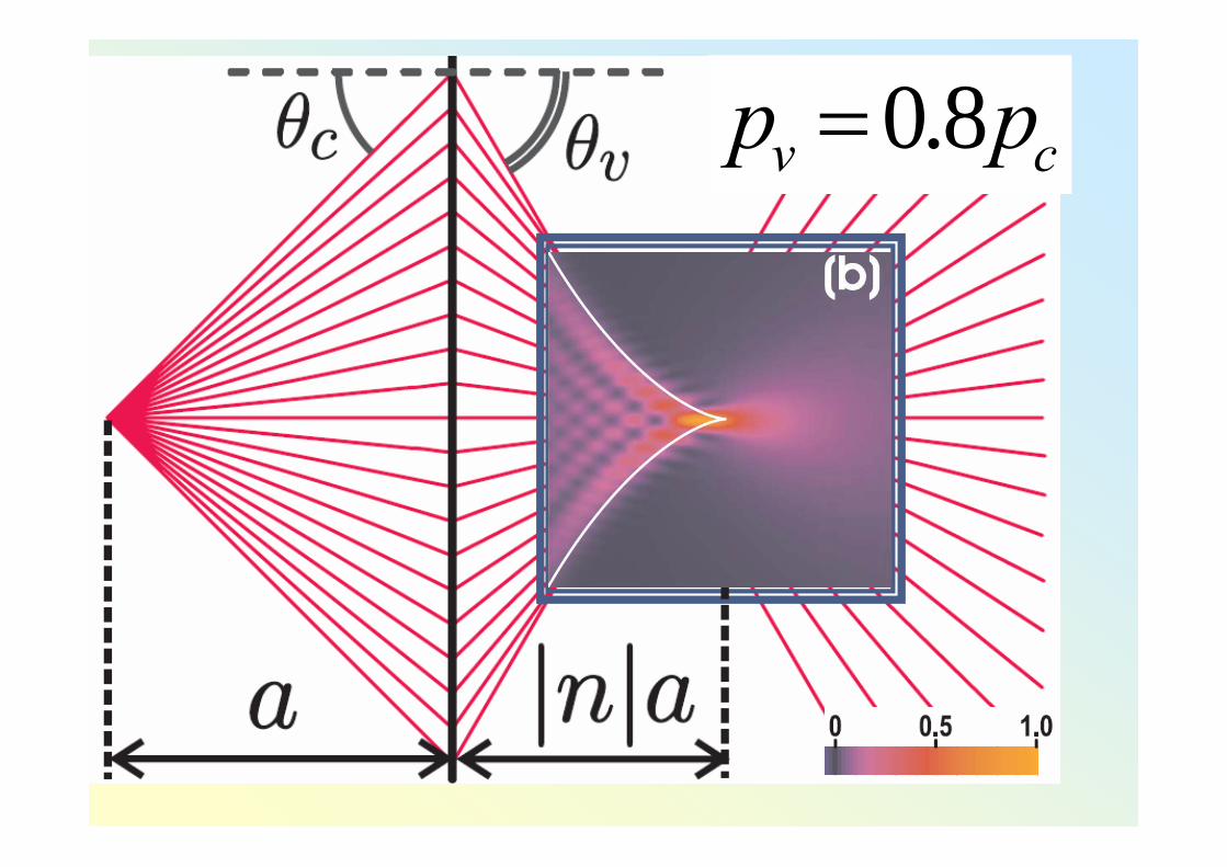
Wishful thinking about graphene microstructuresFocusing and Veselago lens for electrons in ballistic graphene
Cheianov, VF, Altshuler - Science 315, 1252 (2007)
The effect we’ll discuss would be the strongest in sharp PN junction, with d~λF .
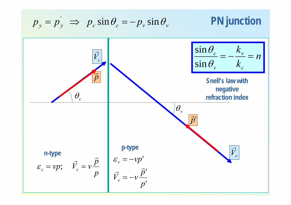
ppvVvp cc
rr== ;ε
pr
cθ
cVr
n-type
vvccyy pppp θθ sinsin' −=⇒=
nkk
c
v
v
c =−=θθ
sinsin
Snell’s law with negative
refraction index
''
'
ppvV
vp
v
vrr
−=
−=ε
'prvθ
vVrp-type
PN junction
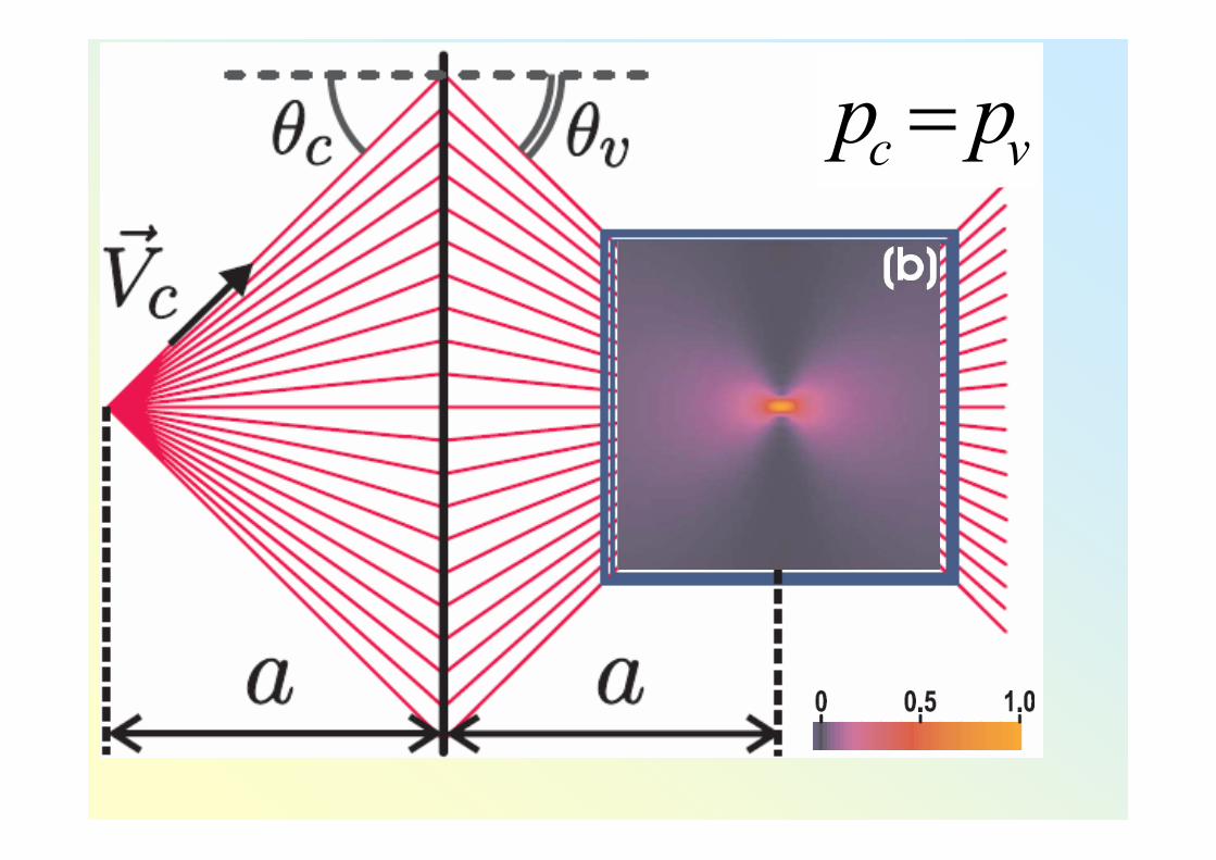
vc pp =
cv pp 8.0=
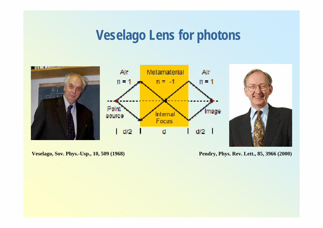
Veselago Lens for photons
Veselago, Sov. Phys.-Usp., 10, 509 (1968) Pendry, Phys. Rev. Lett., 85, 3966 (2000)
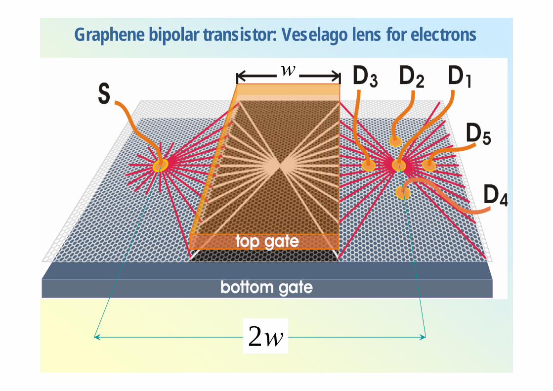
Graphene bipolar transistor: Veselago lens for electrons
w2
w
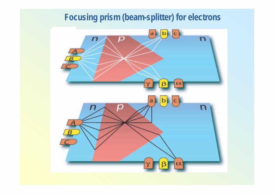
Focusing prism (beam-splitter) for electrons
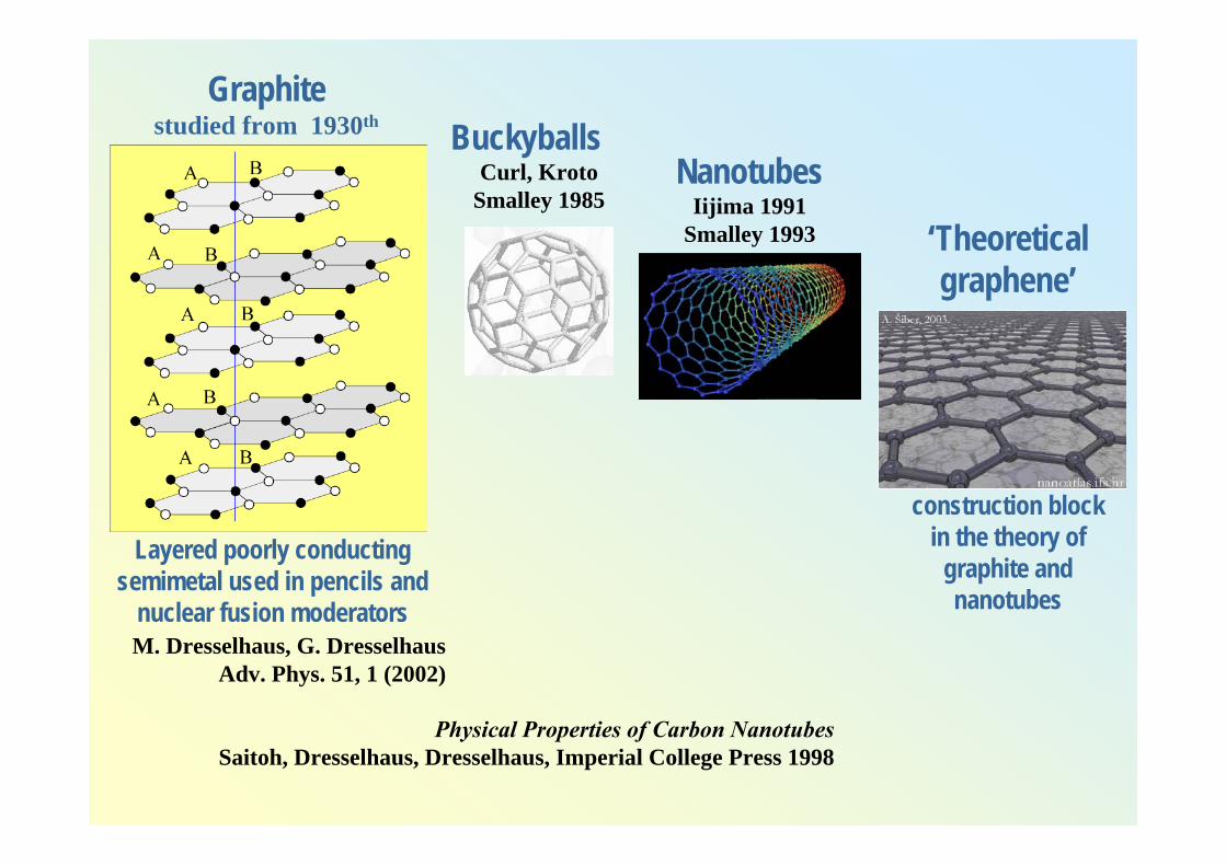
Layered poorly conducting semimetal used in pencils and
nuclear fusion moderatorsM. Dresselhaus, G. Dresselhaus
Adv. Phys. 51, 1 (2002)
Graphitestudied from 1930th
‘Theoretical graphene’
construction block in the theory of
graphite and nanotubes
Physical Properties of Carbon NanotubesSaitoh, Dresselhaus, Dresselhaus, Imperial College Press 1998
BuckyballsCurl, Kroto
Smalley 1985Nanotubes
Iijima 1991Smalley 1993
![Strain Effect on Electronic Structure and Work Function in ... › 0045 › 168f0eb4bb6...for structural and magnetic properties. Mosey et al. [23] obtained better overall agreement](https://static.fdocument.org/doc/165x107/5f226267f839ad1a5f39a142/strain-effect-on-electronic-structure-and-work-function-in-a-0045-a-168f0eb4bb6.jpg)