Electron Transport in Molecules, Nanotubes and...
34
Electron Transport in Molecules, Nanotubes and Graphene Philip Kim Department of Physics Columbia University
Transcript of Electron Transport in Molecules, Nanotubes and...
Electron Transport in Molecules, Nanotubes and Graphene
Philip Kim
Department of PhysicsColumbia University
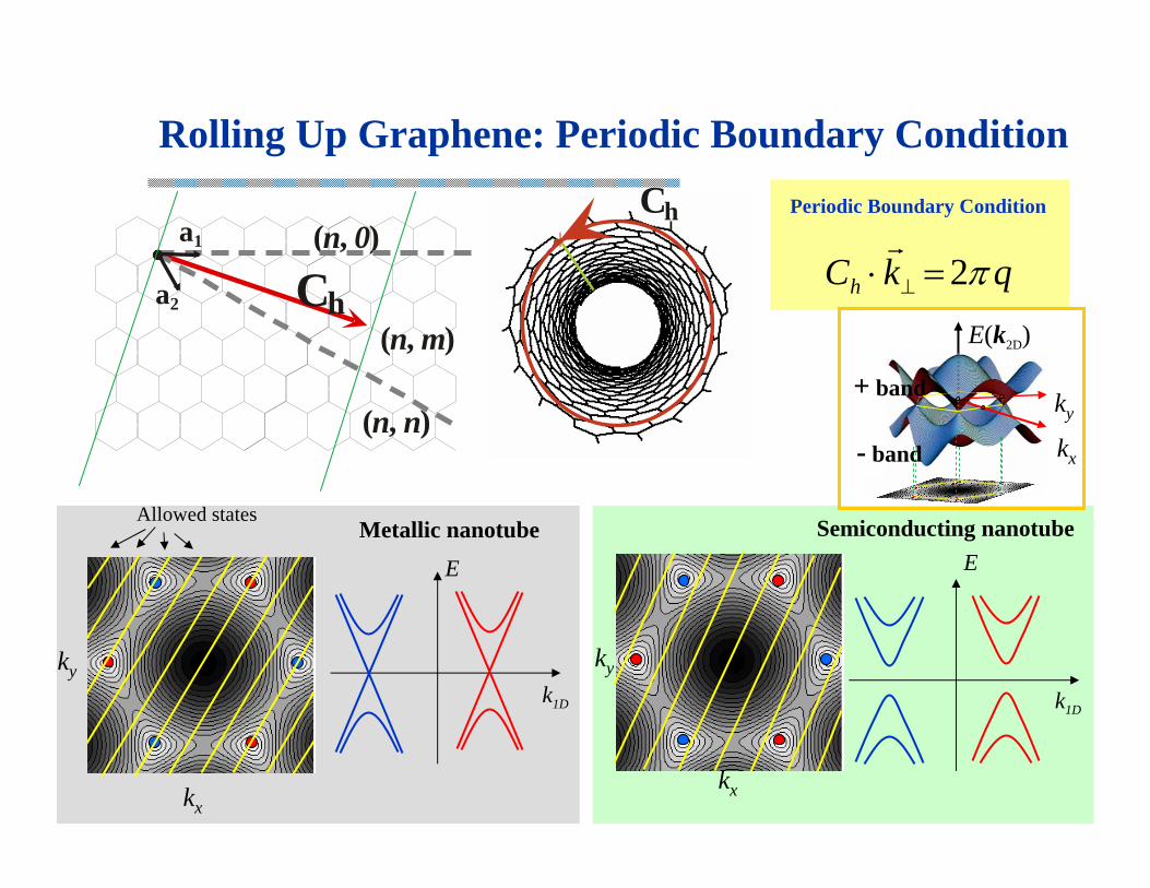
ky
kx
Rolling Up Graphene: Periodic Boundary Condition
(n, 0)
(n, n)
Ch(n, m)
a1
a2
Ch Periodic Boundary Condition
qkCh π2=⋅ ⊥
r
kx
ky
Allowed statesMetallic nanotube
E
k1D
E
k1D
Semiconducting nanotube
x
E(k2D)
kx
ky+ band
- band
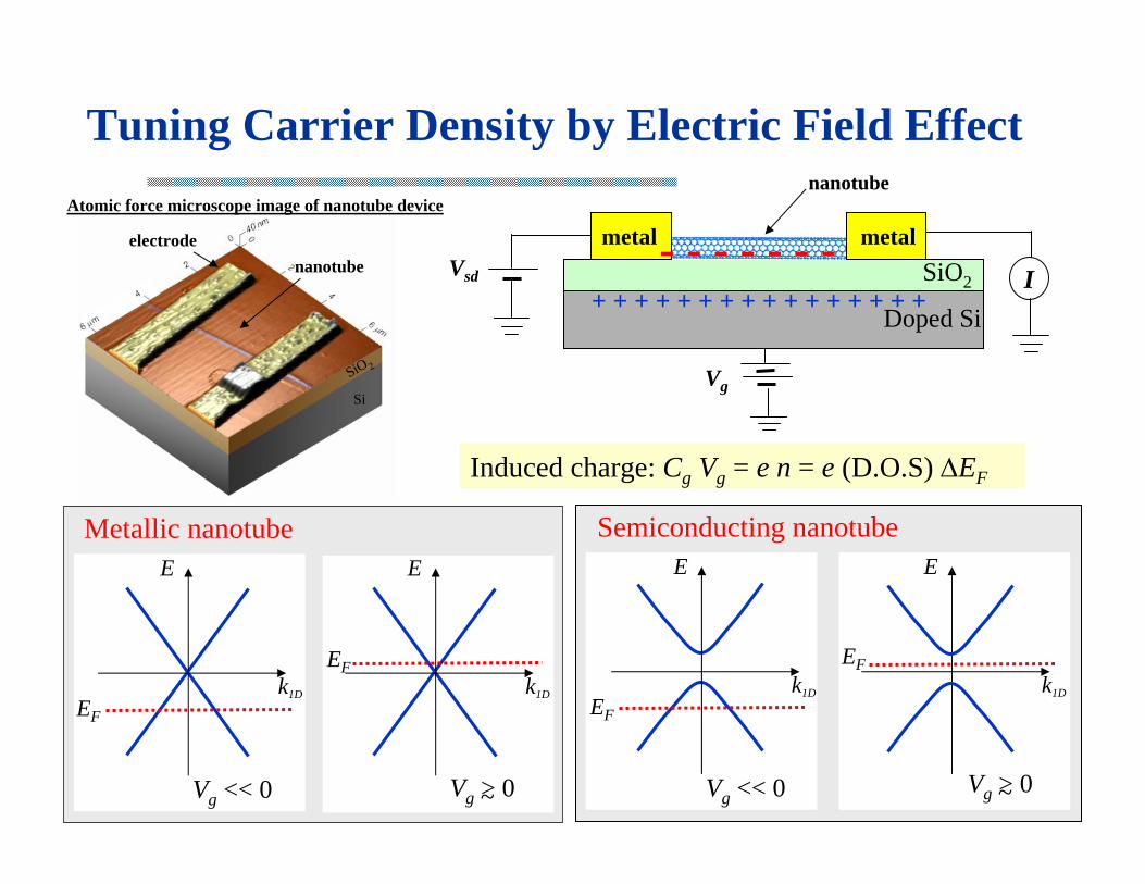
Tuning Carrier Density by Electric Field Effect
Vg
Vsd IDoped Si
SiO2
metalmetal
nanotube
+ + + + + + + + + + + + + + + +
- - - - - - -
Induced charge: Cg Vg = e n = e (D.O.S) ∆EF
E
k1DEF
E
k1D
EF
Vg << 0
Metallic nanotube
Vg > 0~
E
k1DEF
E
k1D
EF
Vg << 0
Semiconducting nanotube
Vg > 0~
Atomic force microscope image of nanotube device
nanotubeelectrode
SiO 2
Si
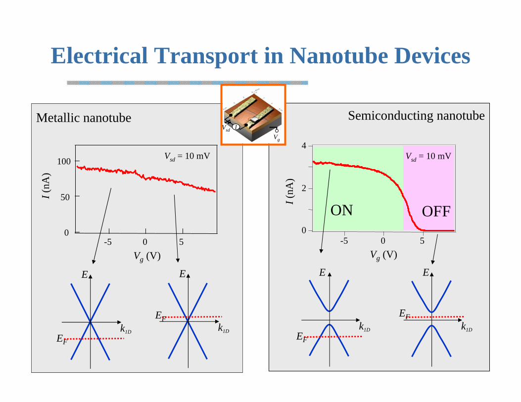
OFFON
Electrical Transport in Nanotube Devices
E
k1DEF
E
k1D
EF
100
50
050-5
Vsd = 10 mV
Vg (V)
I(nA
)
E
k1DEF
Metallic nanotube
E
k1D
EF
Vg (V)
4
2
0-5 0 5
I(nA
)
Vsd = 10 mV
Semiconducting nanotubeIVsd
Vg
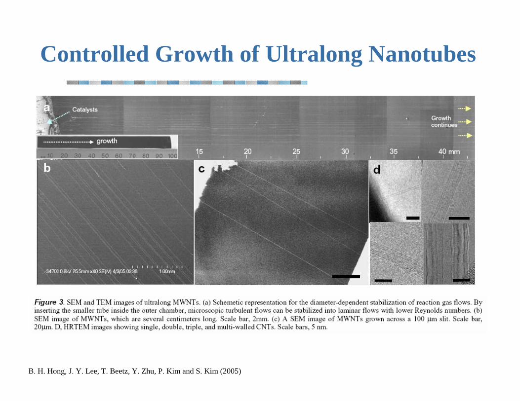
Controlled Growth of Ultralong Nanotubes
B. H. Hong, J. Y. Lee, T. Beetz, Y. Zhu, P. Kim and S. Kim (2005)
(Avouris, IBM)
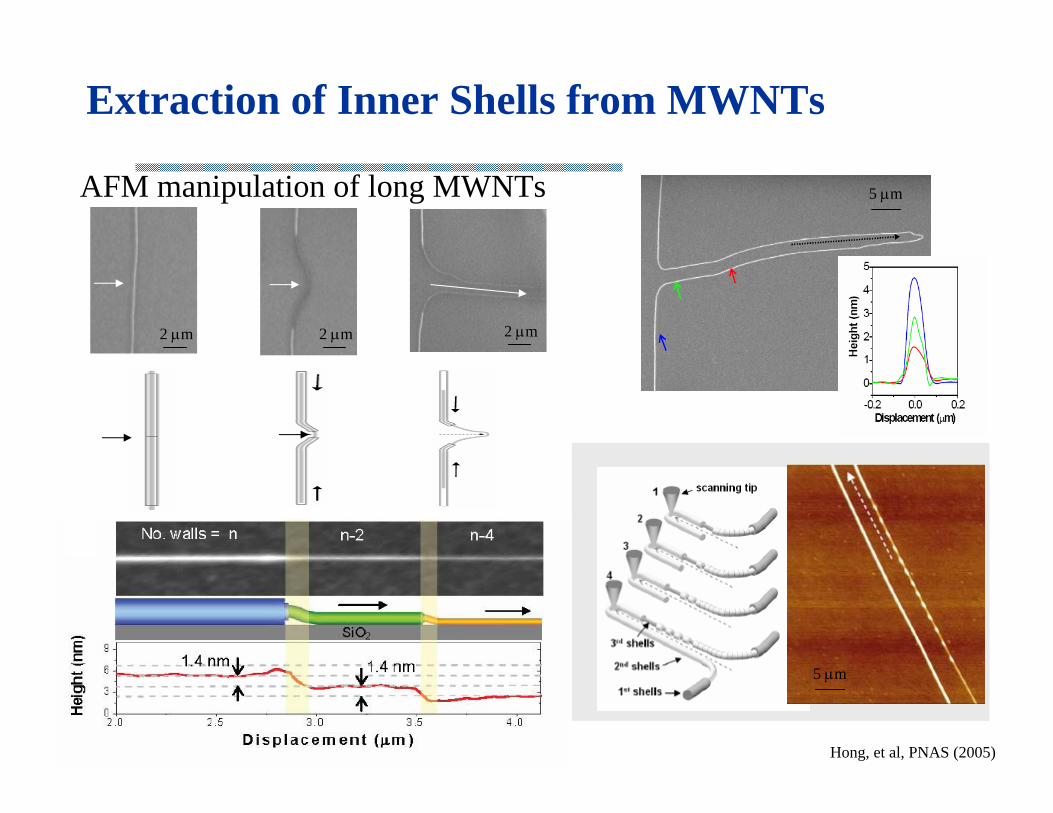
Extraction of Inner Shells from MWNTs
Hong, et al, PNAS (2005)
AFM manipulation of long MWNTs
2 µm
5 µm
2 µm 2 µm
5 µm
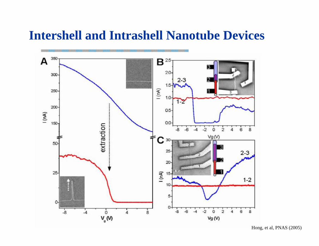
Intershell and Intrashell Nanotube Devices
Hong, et al, PNAS (2005)
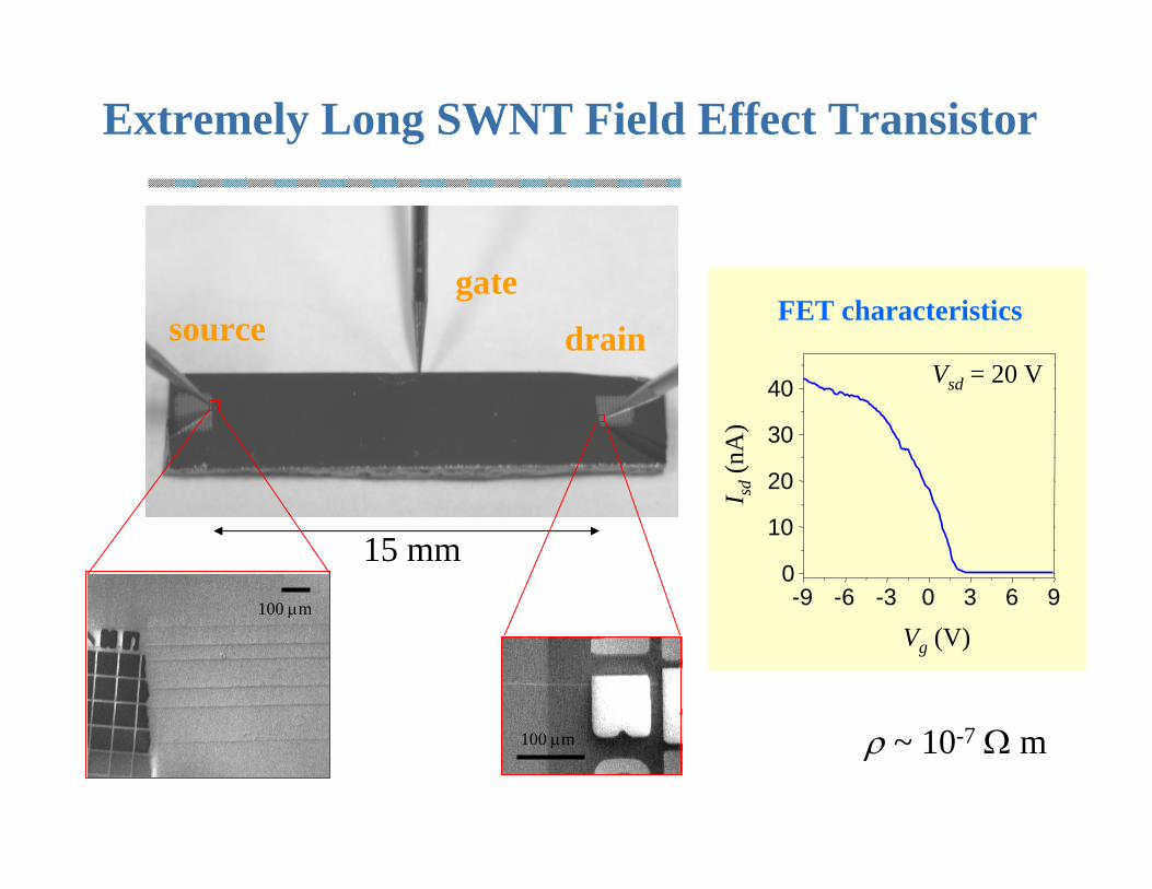
15 mm
Extremely Long SWNT Field Effect Transistor
gatesource drain
100 µm
100 µm
FET characteristics
-9 -6 -3 0 3 6 90
10
20
30
40
Vg (V)
I sd(n
A)
Vsd = 20 V
ρ ~ 10-7 Ω m
400
200
0
6040200
Length (µm)
Res
ista
nce
(kΩ
)
T = 250 K
ρ = 8 kΩ/µm
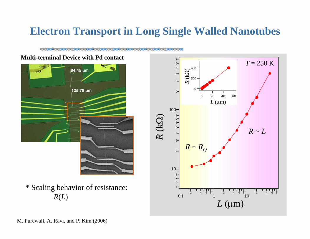
Electron Transport in Long Single Walled Nanotubes
Multi-terminal Device with Pd contact
M. Purewall, A. Ravi, and P. Kim (2006)
* Scaling behavior of resistance:R(L)
5678
10
2
3
4
5678
100
2
3
4
567
0.12 4 6 8
12 4 6 8
102 4 6 8
L (µm)
R(kΩ
)
T = 250 K400
200
0
6040200
R(kΩ
)
L (µm)
R ~ RQ
R ~ L
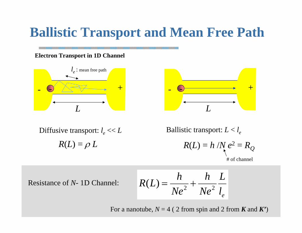
- +-
L
Ballistic Transport and Mean Free PathElectron Transport in 1D Channel
le : mean free path
R(L) = ρ LDiffusive transport: le << L
- +-
L
Ballistic transport: L < le
Resistance of N- 1D Channel:
For a nanotube, N = 4 ( 2 from spin and 2 from K and K’)
elL
Neh
NehLR 22)( +=
R(L) = h /N e2 = RQ
# of channel
5
6789
10
2
3
4
5
6789
100
2
3
4
5
67
2 3 4 5 61
2 3 4 5 610
2 3 4 5 6100
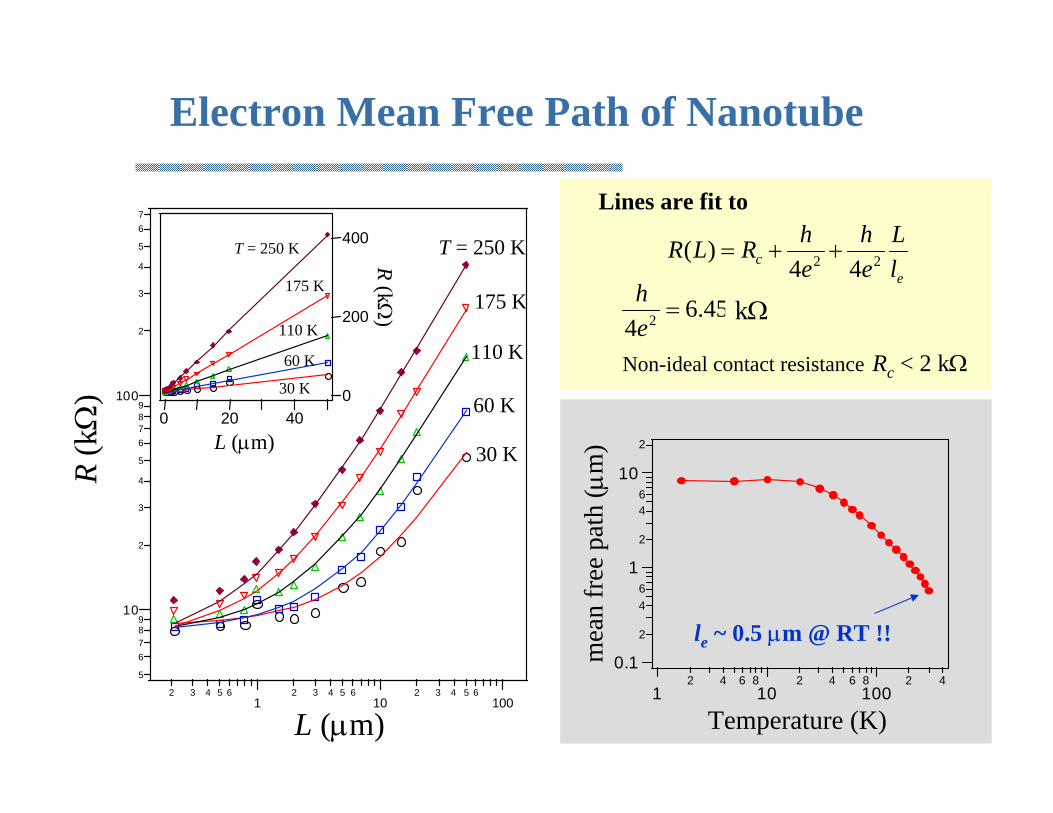
Electron Mean Free Path of Nanotube
L (µm)
R(kΩ
)
T = 250 K
175 K
110 K
60 K
30 K
400
200
040200
L (µm)
R(kΩ
)
T = 250 K
175 K
110 K
60 K
30 K
ec l
Leh
ehRLR 22 44
)( ++=
Lines are fit to
45.64 2 =eh
kΩ
Non-ideal contact resistance Rc < 2 kΩ
Temperature (K)
mea
n fr
ee p
ath
(µm
)
0.1
2
46
1
2
46
10
2
12 4 6 8
102 4 6 8
1002 4
le ~ 0.5 µm @ RT !!
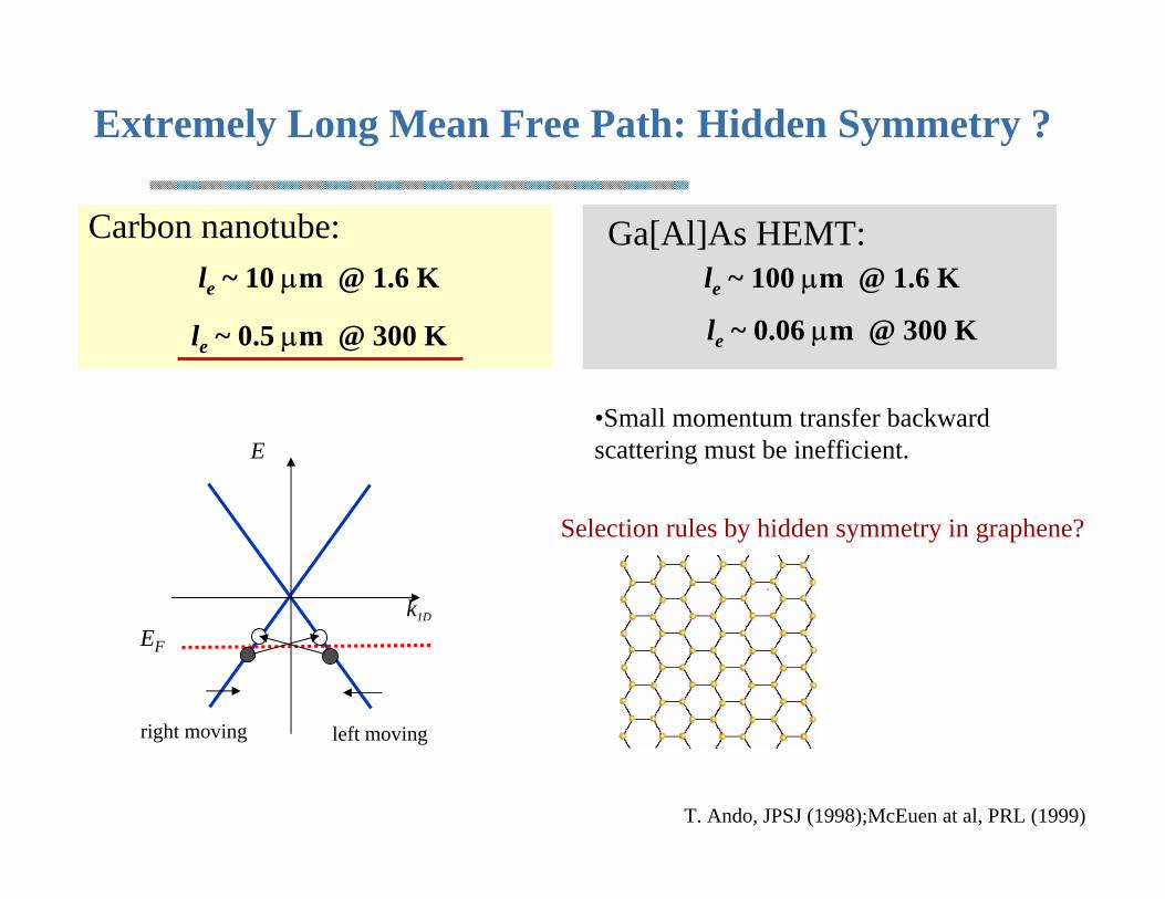
Extremely Long Mean Free Path: Hidden Symmetry ?
le ~ 0.5 µm @ 300 K
le ~ 10 µm @ 1.6 K
Carbon nanotube: Ga[Al]As HEMT:le ~ 100 µm @ 1.6 K
le ~ 0.06 µm @ 300 K
E
k1D
EF
right moving left moving
•Small momentum transfer backward scattering must be inefficient.
Selection rules by hidden symmetry in graphene?
T. Ando, JPSJ (1998);McEuen at al, PRL (1999)
Electric Field Effect in Mesoscopic Graphite
Simple Yet Efficient Mechanical Extraction
Using Scotch Tape is Essential!!
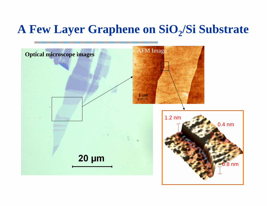
1 µm
AFM Image
A Few Layer Graphene on SiO2/Si Substrate
0.8 nm
0.4 nm1.2 nm
Optical microscope images
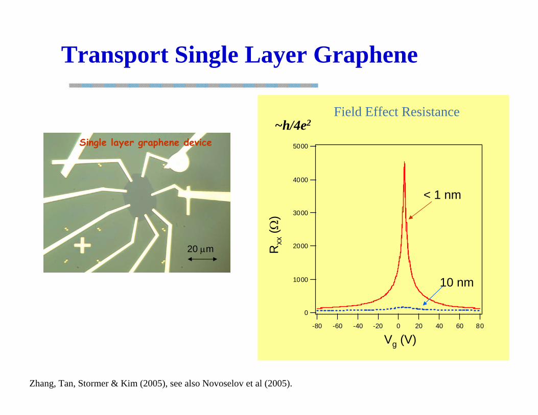
Transport Single Layer Graphene
Cleaved graphite crystallite
20 µm
Single layer graphene device 5000
4000
3000
2000
1000
0
-80 -60 -40 -20 0 20 40 60 80
Vg (V)
Rxx
(Ω)
< 1 nm
10 nm
Field Effect Resistance~h/4e2
Zhang, Tan, Stormer & Kim (2005), see also Novoselov et al (2005).
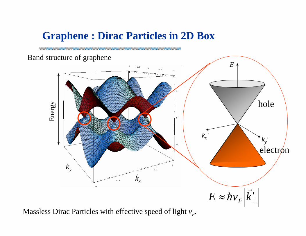
Graphene : Dirac Particles in 2D Box
Band structure of graphene
kx
ky
Ener
gy
kx' ky'
E
⊥′≈ kvE F
rh
Massless Dirac Particles with effective speed of light vF.
hole
electron
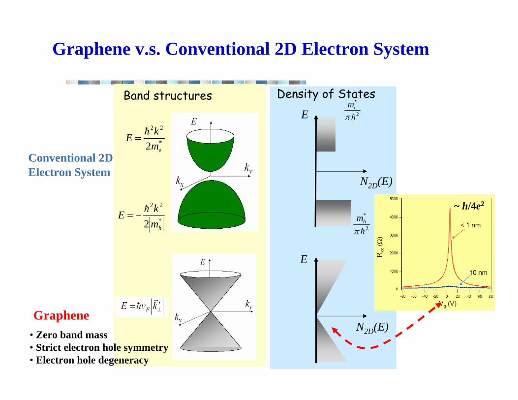
Graphene v.s. Conventional 2D Electron System
Conventional 2D Electron System
Graphene
E
N2D(E)
*
22
2 emkE h
=
*
22
2 hmkE h
−=
N2D(E)
E 2
*
hπem
2
*
hπhm
Band structures Density of States
• Zero band mass• Strict electron hole symmetry• Electron hole degeneracy
~ h/4e2
DOS
E
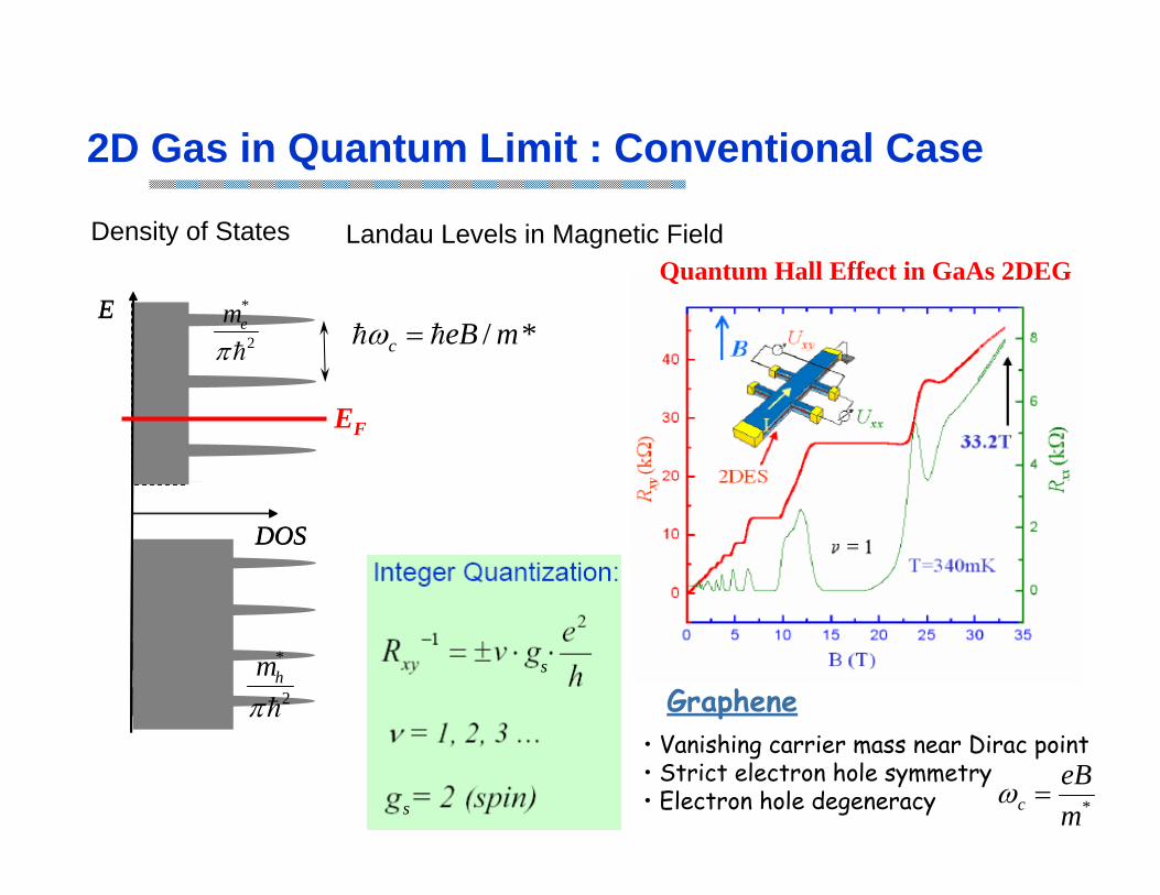
2D Gas in Quantum Limit : Conventional Case
DOS
E2
*
hπem
2
*
hπhm
Density of States
*/ meBc hh =ω
Landau Levels in Magnetic FieldQuantum Hall Effect in GaAs 2DEG
s
s
EF
Graphene• Vanishing carrier mass near Dirac point• Strict electron hole symmetry• Electron hole degeneracy *m
eBc =ω
15
10
5
086420
6
4
2
0
Hal
l Res
ista
nce
(kΩ
)
Magnetoresistance (kΩ
)B (T)
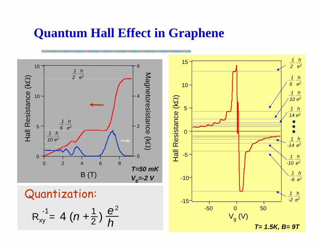
Quantum Hall Effect in Graphene
____ he2
12
____ he2
16
____ he2
110
T=50 mK
____ he2
12
-15
-10
-5
0
5
10
15
-50 0 50Vg (V)
Hal
l Res
ista
nce
(kΩ
)
T= 1.5K, B= 9T
____ he2
16
____ he2
110
____ he2
114
h1 ____e2-14
e2____ h1
-10
____ he2
1-6
____ he2
1-2
Quantization:
4 (n + )Rxy =-1 ___ e
h2
21
Vg=-2 V
EF
σxy
Ene
rgy
gse2/h
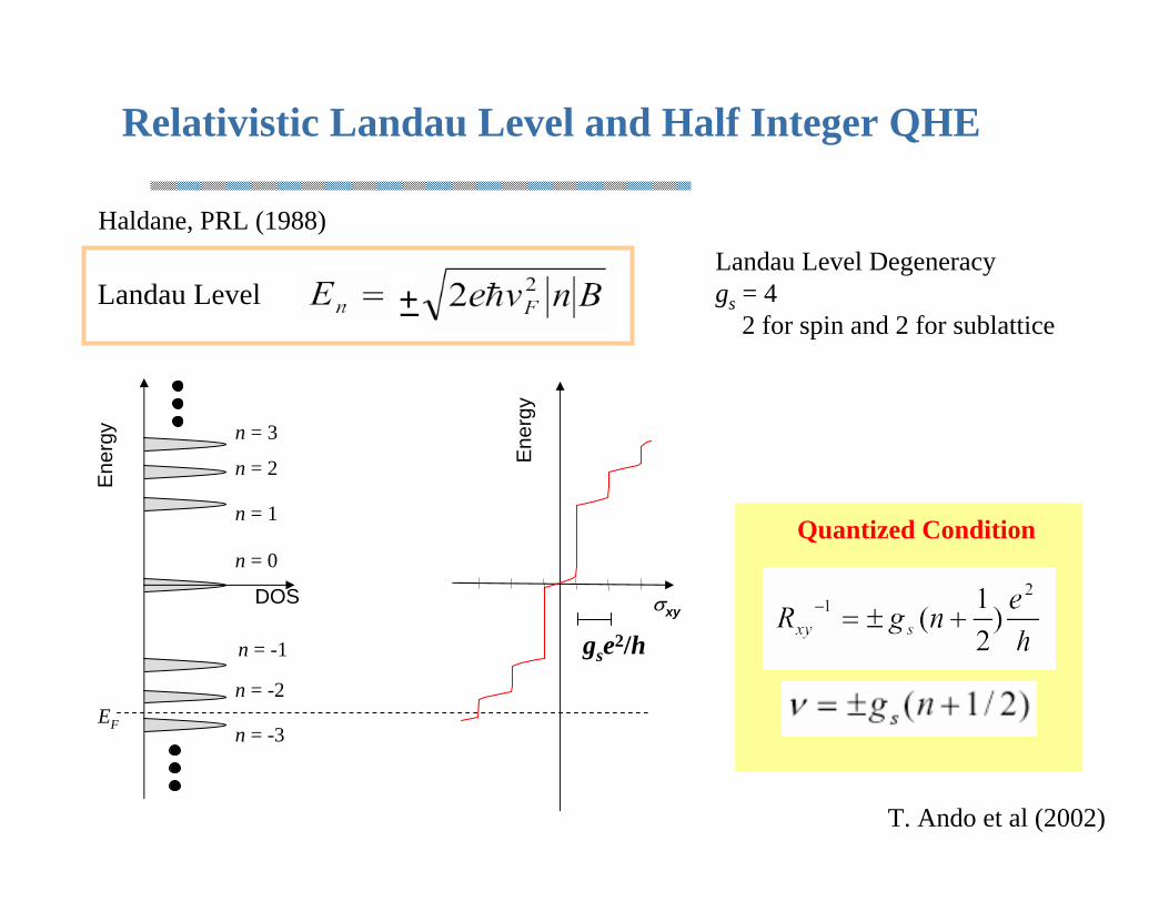
Relativistic Landau Level and Half Integer QHE
Landau Level +_Landau Level Degeneracygs = 4
2 for spin and 2 for sublattice
Quantized Condition
Haldane, PRL (1988)
T. Ando et al (2002)
n = 1
n = 2
n = 3
n = -3
n = 0
n = -1
n = -2
DOS
Ene
rgy
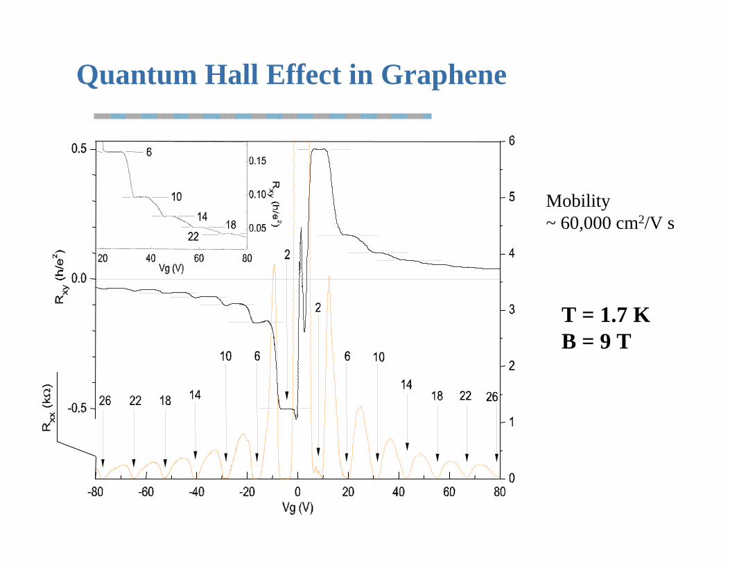
Quantum Hall Effect in Graphene
T = 1.7 KB = 9 T
Mobility ~ 60,000 cm2/V s
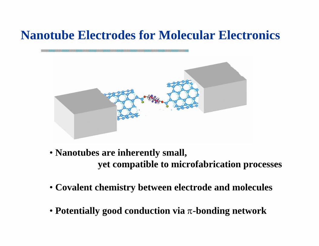
Nanotube Electrodes for Molecular Electronics
• Nanotubes are inherently small, yet compatible to microfabrication processes
• Covalent chemistry between electrode and molecules
• Potentially good conduction via π-bonding network
Nanotube device
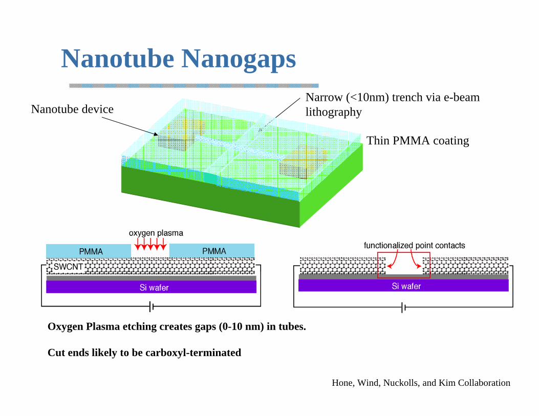
Nanotube Nanogaps
Thin PMMA coating
Narrow (<10nm) trench via e-beam lithography
Oxygen Plasma etching creates gaps (0-10 nm) in tubes.
Cut ends likely to be carboxyl-terminated
Hone, Wind, Nuckolls, and Kim Collaboration
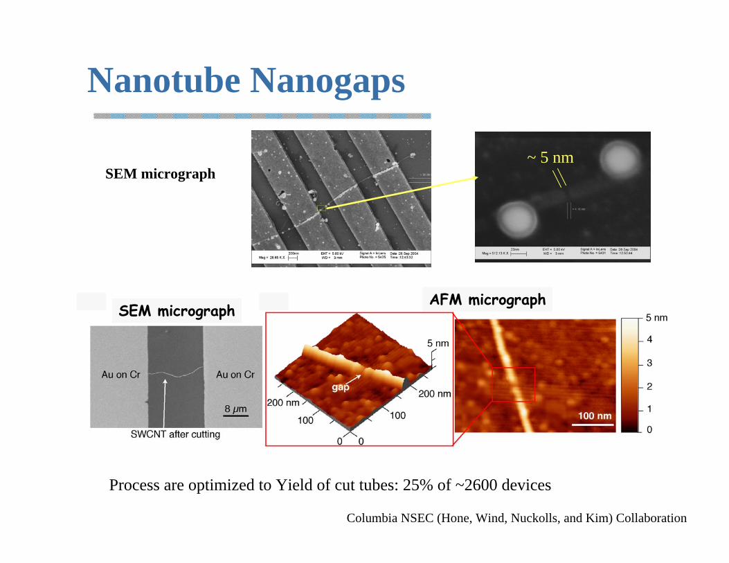
Process are optimized to Yield of cut tubes: 25% of ~2600 devices
AFM micrographSEM micrograph
Nanotube Nanogaps
~ 5 nmSEM micrograph
Columbia NSEC (Hone, Wind, Nuckolls, and Kim) Collaboration
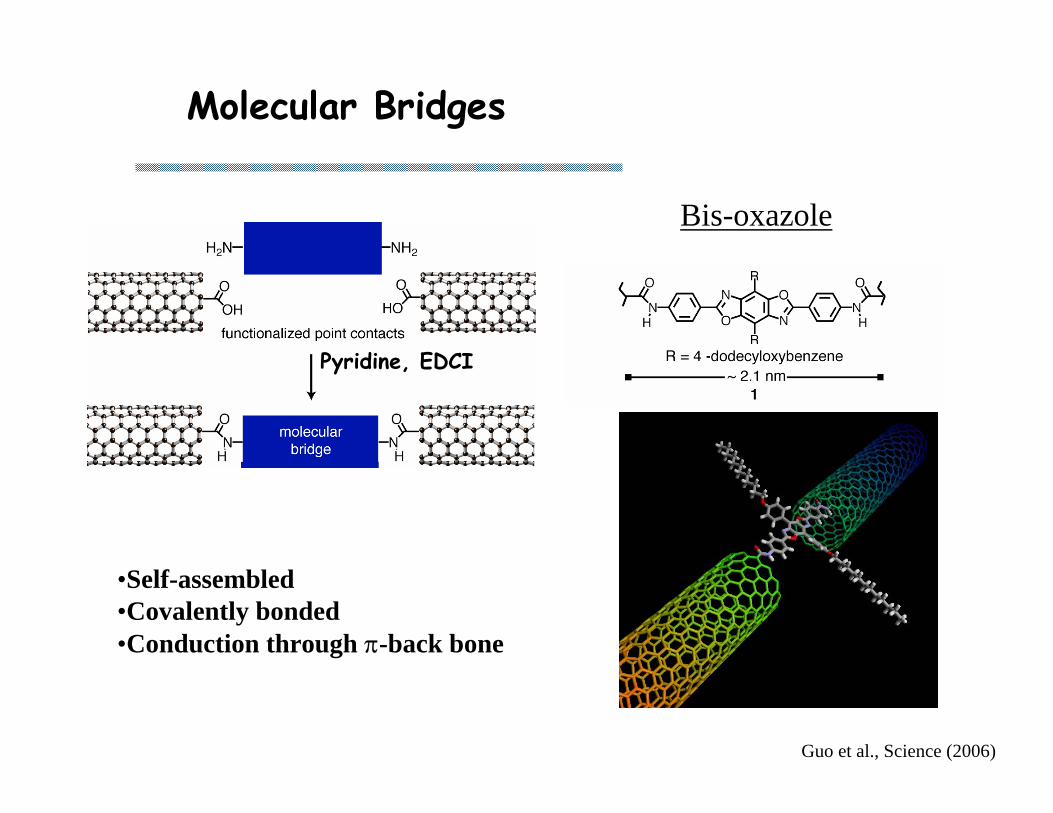
Molecular Bridges
Pyridine, EDCI
•Self-assembled•Covalently bonded•Conduction through π-back bone
Bis-oxazole
Guo et al., Science (2006)
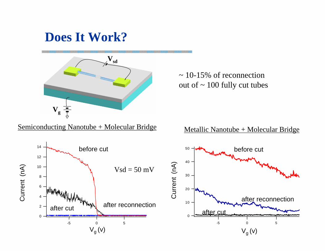
Does It Work?
50
40
30
20
10
0
-5 0 5
Vg (v)
Cur
rent
(nA
)
before cut
after cut
after reconnection
Metallic Nanotube + Molecular Bridge
Vsd
~ 10-15% of reconnectionout of ~ 100 fully cut tubes
after reconnection
Semiconducting Nanotube + Molecular Bridge
after cut
Vg (v)
Cur
rent
(nA
)
before cut
Vsd = 50 mV
14
12
10
8
6
4
2
0
-5 0 5
Vg
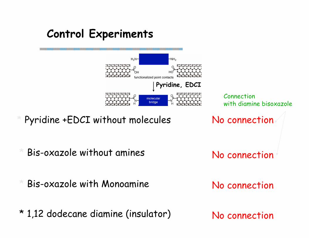
* Pyridine +EDCI without molecules No connection
* Bis-oxazole without amines No connection
* Bis-oxazole with Monoamine No connection
* 1,12 dodecane diamine (insulator) No connection
Connection with diamine bisoxazole
Control Experiments
Pyridine, EDCI
Pyridine, EDCI
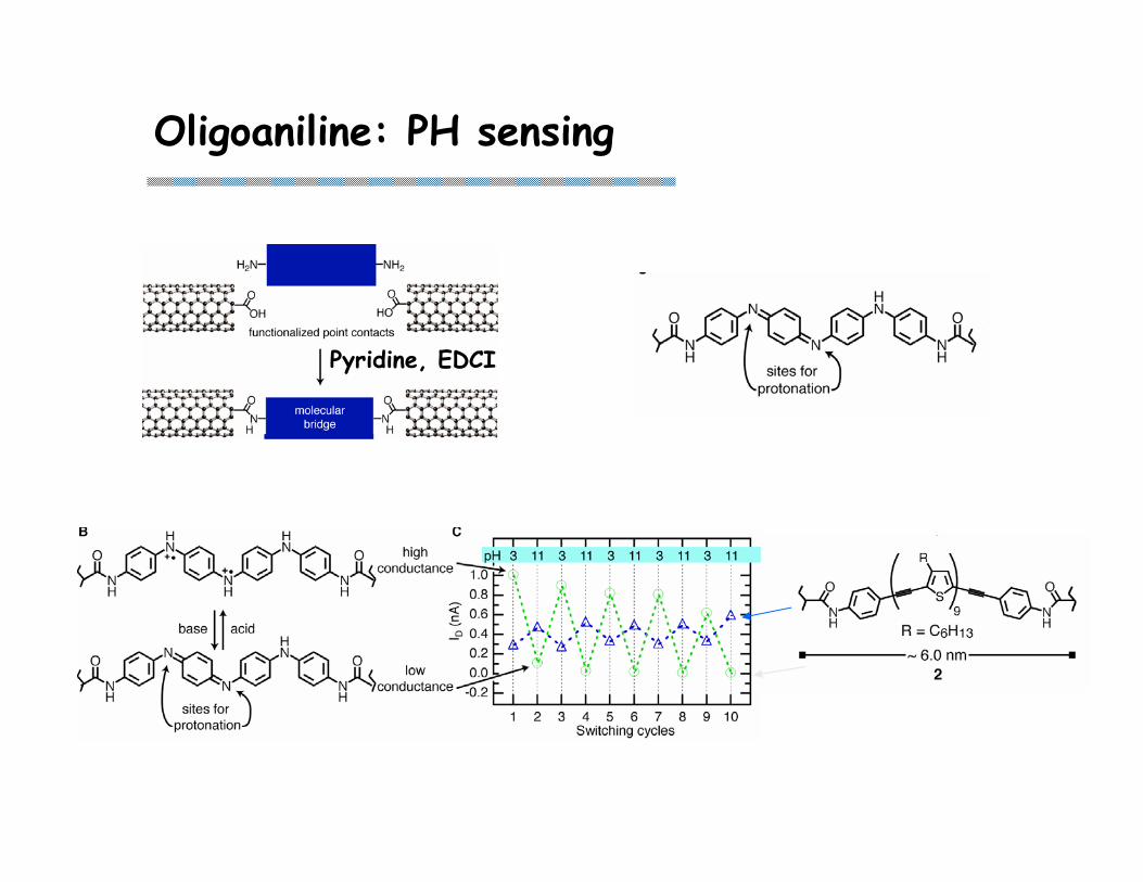
Oligoaniline: PH sensing
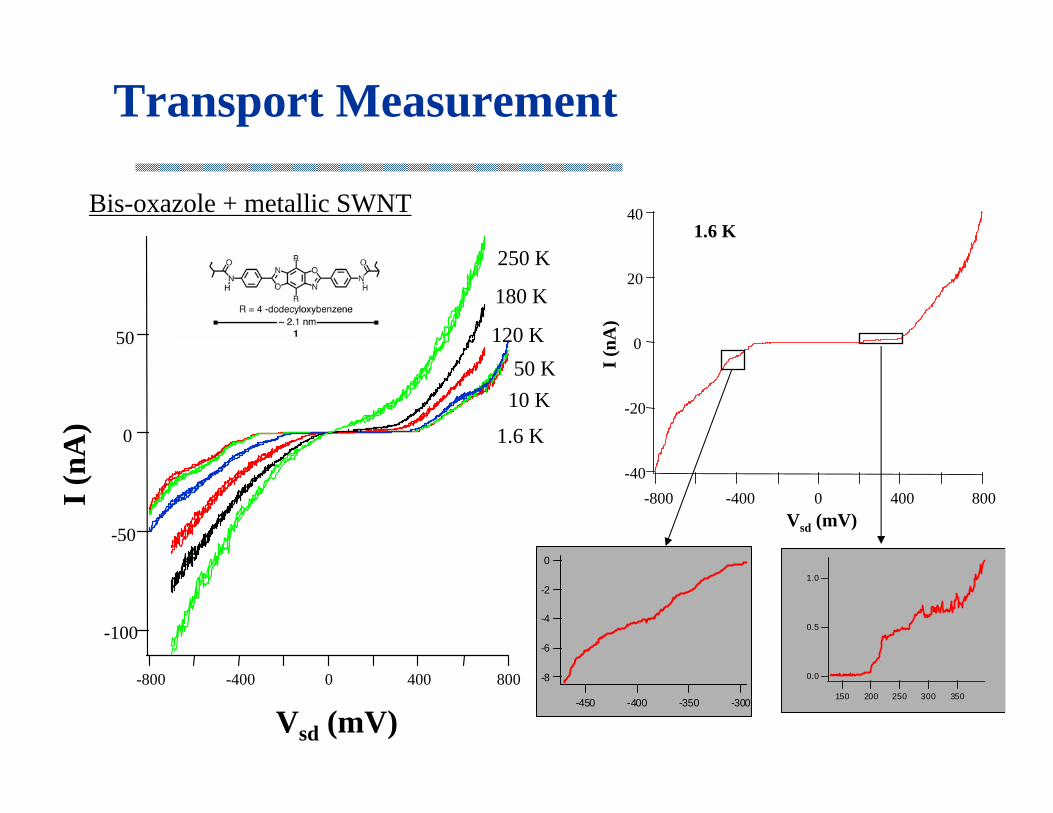
Transport Measurement
-100
-50
0
50
-800 -400 0 400 800
250 K
180 K
120 K50 K
10 K
1.6 K
Vsd (mV)
I (nA
)
Bis-oxazole + metallic SWNT
I (nA
)
40
20
0
-20
-40-800 -400 0 400 800
Vsd (mV)
1.6 K
-8
-6
-4
-2
0
-450 -400 -350 -300
1.0
0.5
0.0
350300250200150
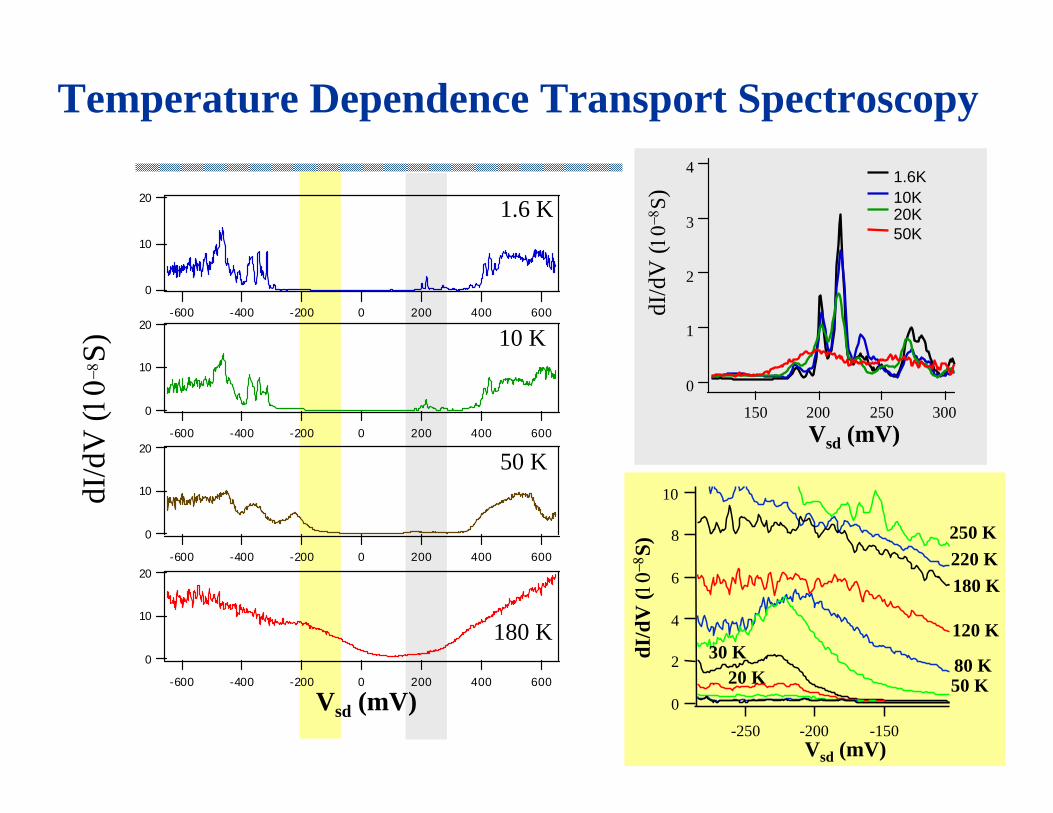
Temperature Dependence Transport Spectroscopy
20
10
0
-600 -400 -200 0 200 400 60020
10
0
-600 -400 -200 0 200 400 60020
10
0
-600 -400 -200 0 200 400 60020
10
0
-600 -400 -200 0 200 400 600
1.6 K
10 K
50 K
180 K
Vsd (mV)
dI/d
V(10−
8 S)
4
3
2
1
0
300250200150
1.6K10K20K50K
Vsd (mV)
dI/d
V(10−
8 S)
10
8
6
4
2
0
-250 -200 -150Vsd (mV)
dI/d
V(10−
8 S)
30 K
50 K80 K
120 K
180 K220 K250 K
20 K
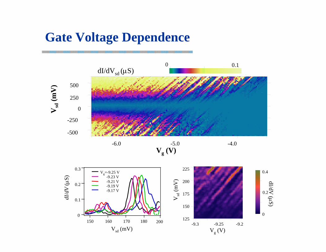
Gate Voltage Dependence
Vg (V)
Vsd
(mV
)
150
175
200
225
125-9.3 -9.25 -9.2
0
0.2
0.4
dI/dV(µS)
0.3
0.2
0.1
0180170160150
Vg=-9.25 V-9.23 V-9.21 V-9.19 V-9.17 V
Vsd (mV)
dI/d
V(µ
S)
200
-5.0-6.0 -4.0
-500
-250
250
500
0
Vg (V)
Vsd
(mV
)
dI/dVsd (µS)0 0.1
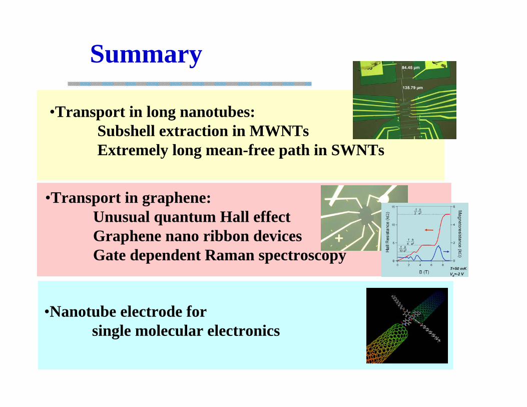
Summary
•Nanotube electrode for single molecular electronics
•Transport in graphene:Unusual quantum Hall effectGraphene nano ribbon devicesGate dependent Raman spectroscopy
•Transport in long nanotubes:Subshell extraction in MWNTsExtremely long mean-free path in SWNTs
AcknowledgementSpecial Thanks to: Yuanbo ZhangMeninder PurewalByung Hee HongJosh SmallMelinda HanBarbaros Oezyilmaz
Kim Group 2004 Summer Central Park
Funding:
Collaboration: Stormer, Pinczuk, Heinz, Nuckolls, Brus, Flynne, Hone,
![Fullerene Derivatives (CN-[OH]β) and Carbon Nanotubes ...](https://static.fdocument.org/doc/165x107/627f787abc5d8f553f2a99ec/fullerene-derivatives-cn-oh-and-carbon-nanotubes-.jpg)