Electron Beam Lithography - University of Texas at Austin
17
Electron Beam Lithography Adam Ramm
Transcript of Electron Beam Lithography - University of Texas at Austin

Electron Beam Lithography
Adam Ramm

Why use electrons?
Negligible diffraction limitations:
𝑅 = 𝑘𝜆
𝑁𝐴
With current optical technology, this equates to about 45nm resolution.
For an electron, wavelength is calculated from its momentum:
𝜆 =ℎ
𝑝=
ℎ
2 ∗ 𝑚𝑒 ∗ 𝑒 ∗ 𝑉𝑎
An accelerating voltage of 1V has λ = 1.2 nm, and 1000V has λ = 0.03 nm.

Generating an electron beam:
Electrode gun:
http://www.didaktik.physik.uni-muenchen.de/elektronenbahnen/en/kanone/klassisch/Aufbau.php

Guiding electrons to the resist:
Can use magnetic or electric fields for lenses
Pimpin, Alongkorn & Srituravanich, Werayut. (2012). Review on Micro- and Nanolithography Techniques and Their Applications. Engineering Journal. 16. 37-56. 10.4186/ej.2012.16.1.37.

Are electrons the answer? Not yet...
Resolution limits from electron scattering:
• Forward scattering (in resist)
• Backscattering (from substrate)
https://slideplayer.com/slide/6000514/
• Resolution now ~25 nm lines and spaces

Proximity Effects
The proximity of closely packed shapes affects the amount of exposure each one sees.
When the densely packed areas are properly exposed, the edges and thin lines are under-exposed.
Varying the electron dose at each location helps alleviate this problem, but makes the process much more complicated.

Proximity Correction
Adjusting the electron exposure based on the pattern location can reduce proximity effects.
The Point Spread Function (PSF) determines the Gaussian shape of the actual resist exposure given the electron beam’s point-like areal coverage.
For electron beams, proximity correction can be done in two ways:• Adjusting the electron dose at locations that require more/less electrons for
proper exposure.• Adjusting pattern dimensions using methods similar to Optical Proximity
Correction methods (write a shape that is different than target shape).

Proximity Correction
Adjusting the electron exposure based on the pattern location can reduce proximity effects.
Vary dose at edges and thin lines
https://ebeam.mff.uw.edu/ebeamweb/doc/patternprep/patternprep/proximity_main.html
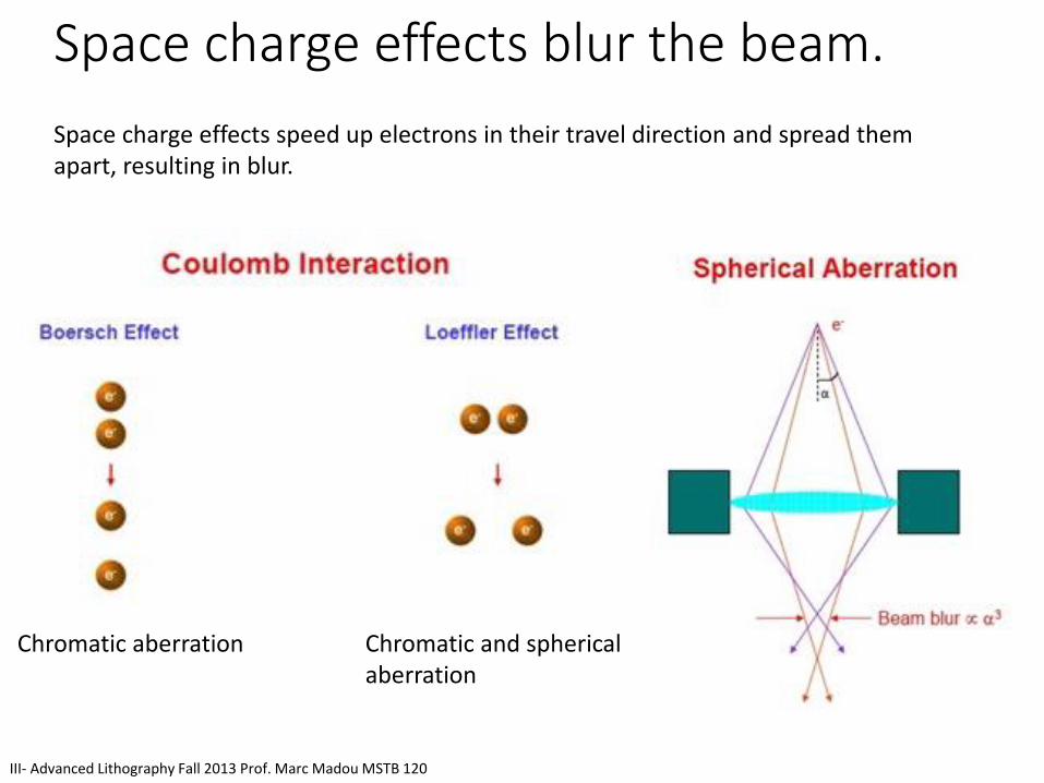
Space charge effects blur the beam.
III- Advanced Lithography Fall 2013 Prof. Marc Madou MSTB 120
Space charge effects speed up electrons in their travel direction and spread them apart, resulting in blur.
Chromatic aberration Chromatic and spherical aberration

Current single beam writing speed is not enough
The minimum time to expose a given area for a given dose:
D * A = T * I
Where:
• D = dose at resist
• A = exposed area
• T = exposure time
• I = beam current
Example:
For 1 cm^2 area, 10^-3 C/cm^2 dose, and 10 nA current, writing time is 10^6
seconds. For a 300mm wafer (700 cm^2), write time, not including stage
movement and beam blanking time, would be > 22 years.
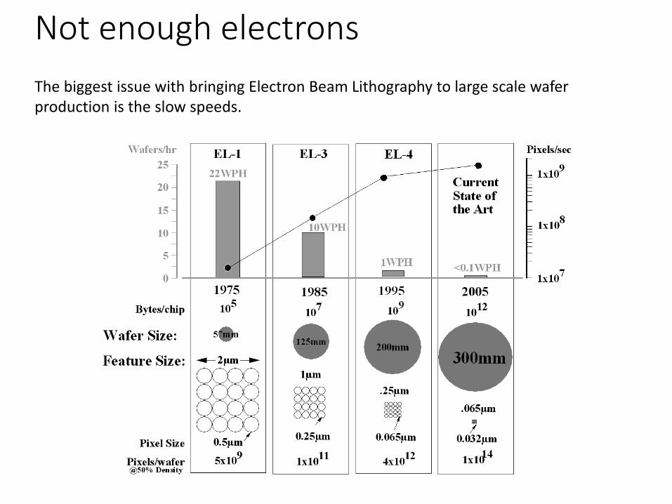
Not enough electrons
The biggest issue with bringing Electron Beam Lithography to large scale wafer production is the slow speeds.

MEBES IV – Bell Labs
Specs:• Write 1X and 5X reticles• target device was 64-Mbit DRAM• 125 x 125 mm writing area• Spot size: 80-400 nm• Position accuracy: 80 nm• Feature size: 250 nm
MEBES employed raster scanning writing:• Chip is divided into stripes• The stage moves in the x-direction while
the beam scans in the y-direction• Used 4-pass writing strategy.
Developed in the 90’s to meet maskmaking requirements of the time.

SCALPEL - Bell Labs
III- Advanced Lithography Fall 2013 Prof. Marc Madou MSTB 120
Specs:• 100 keV electrons• Very little of the total energy reaches the resist.• 4:1 demagnification of the mask.• 70 nm feature sizes possible.• Step and scan method for both the wafer and mask.• ~45 wafers/hour throughput (200mm).
Employed scattering contrast to get images to the wafer:• Mask is low atomic number membrane patterned
with high atomic number material.• Most electrons (high energy) pass through the
mask.• Contrast is generated from the difference in
scattering characteristics in the two mask materials.• Highly scattered electrons are blocked by an
aperture.

REBL - KLA-Tencor
Specs:• 50X demagnification.• 60 nm feature sizes possible.• Electron optics are static system.• 20 Tbps data transfer to DPG required.• ~10 wafers/hour throughput.
• DPG controls ~1 million parallel beams.• Uses reflection instead of transmission.• Rotary stage allows for multiple wafer
processing.• Grey-tone exposure to supply non-binary
doses to resist.
Employed reflective electron optics with a Digital Pattern Generator (DPG):
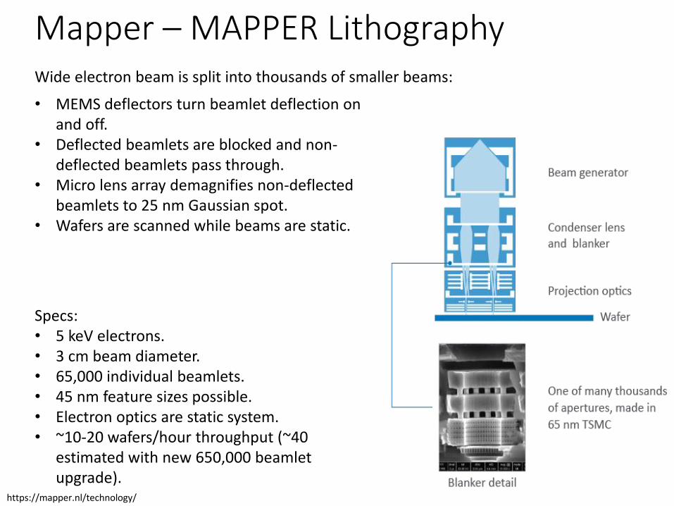
Mapper – MAPPER Lithography
Specs:• 5 keV electrons.• 3 cm beam diameter.• 65,000 individual beamlets.• 45 nm feature sizes possible.• Electron optics are static system.• ~10-20 wafers/hour throughput (~40
estimated with new 650,000 beamletupgrade).
• MEMS deflectors turn beamlet deflection on and off.
• Deflected beamlets are blocked and non-deflected beamlets pass through.
• Micro lens array demagnifies non-deflected beamlets to 25 nm Gaussian spot.
• Wafers are scanned while beams are static.
Wide electron beam is split into thousands of smaller beams:
https://mapper.nl/technology/

IMS – IMS Nanofabrication
Specs:• 5 keV electrons.• 200x demagnification.• 262,000 individual beamlets.• 30 nm feature sizes possible.• Electron optics are static system.• <10 hr mask writing time (current masks can
take 30+ hrs to write).
• Employs programmable aperature plate system.
• Demagnification of beams with magnetic lenses to 20 nm beam spot size
• Wafers are scanned while beams are static.• Throughput is independent of pattern
complexity.
High-throughput multi-beam mask writing:
https://www.ims.co.at/wp-content/uploads/2016-10-17_BACUS-2016_IMS_MBMW-101_998505.pdf

Conclusion
• Electrons beat the diffraction limit associated with optical lithography.
• Electrons can be guided and focused, similarly to photons, by using magnetic or electrostatic lenses.
• Electron scattering is the main limitation of writing small features.
• Proximity correction can help limit scattering effects, but can not get anywhere near the de Broglie limit of electrons.
• Electron throughput severely limits using E-beam technology for large scale production.
• Large area beams and multi-beam systems are the current approach to solving the throughput problem.