Effects of γ-ray radiation on two-dimensional molybdenum disulfide...
5
Effects of c-ray radiation on two-dimensional molybdenum disulfide (MoS 2 ) nanomechanical resonators Jaesung Lee, 1,a) Matthew J. Krupcale, 1,2,a) and Philip X.-L. Feng 1,b) 1 Department of Electrical Engineering and Computer Science, Case School of Engineering, Case Western Reserve University, 10900 Euclid Avenue, Cleveland, Ohio 44106, USA 2 Department of Physics, College of Arts and Sciences, Case Western Reserve University, 10900 Euclid Avenue, Cleveland, Ohio 44106, USA (Received 1 November 2015; accepted 26 December 2015; published online 13 January 2016) We report on experimental investigation and analysis of c-ray radiation effects on two-dimensional molybdenum disulfide (MoS 2 ) drumhead nanomechanical resonators vibrating at megahertz fre- quencies. Given calibrated dosages of c-ray radiation of 5000 photons with energy at 662 keV, upon exposure over 24 or 12 h, all the MoS 2 resonators exhibit 0.5–2.1% resonance frequency upshifts due to the ionizing c-ray induced charges and their interactions. The devices show c-ray photon responsivity of 30–82 Hz/photon, with an intrinsic c-ray sensitivity (limit of detection) estimated to approach 0.02–0.05 photon. After exposure expires, resonance frequencies return to an ordinary tendency where the frequency variations are dominated by long-term drift. These c-ray radiation induced frequency shifts are distinctive from those due to pressure variation or surface adsorption mechanisms. The measurements and analyses show that MoS 2 resonators are robust yet sensitive to very low dosage c-ray, demonstrating a potential for ultrasensitive detection and early alarm of radiation in the very low dosage regime. V C 2016 AIP Publishing LLC. [http://dx.doi.org/10.1063/1.4939685] Radiations such as energetic subatomic particles or pho- tons generated from nuclear reactions 1 have been exploited in a wide range of applications, from basic science (e.g., observ- ing c-ray bursts for studying cosmology 2 ) to industry (e.g., electricity generation in nuclear plants) and nuclear medicine (e.g., imaging). 3 Meanwhile, with sufficient energy, such radi- ations may damage matters by breaking atomic bonds, ioniz- ing atoms, or causing harmful biomolecular effects in living tissues. 3 To safely utilize radiations, it is desirable not only to develop various robust detectors capable of operating in harsh environments with high levels of radiations such as in nuclear reactors, but also to explore highly responsive and sensitive materials and devices for very early alarm of low dosage radi- ations or leakage. In all these scenarios, detection of ionizing radiations is of great importance for identifying, quantifying, and monitoring radiation sources and activities. Historically gas-filled chambers have been the earliest for detecting ionizing radiations via the gas ionization. Since 1940s, scintillation crystals combined with photomultiplier tubes (PMT) have prevailed as the mainstream solutions in many applications to date. Later semiconductor junction devices have been extensively studied for compact pixel and array detectors. 4,5 Among the various possible semiconduc- tor device platforms and detection mechanisms for ionizing radiations, resonant micro/nanoelectromechanical systems (MEMS/NEMS) offer excellent promises and sustainable improvement with device scaling. 6,7 In particular, because NEMS resonances are exceptionally responsive to variations in their modal masses and stiffnesses, considerable interests and efforts have been stimulated in exploiting nanoresonators for ultrasensitive detection of physical quan- tities such as mass and force, attaining yocto-gram (10 24 g) 8 and zepto-newton (10 21 N) 7 sensitivities. Responses of nanoresonators to radiations such as c-ray particles, however, have not yet been reported. Atomic layer crystals, such as graphene and molybdenum disulfide (MoS 2 ), have emerged as advanced materials for 2D electronic, 9,10 mechanical, 11–15 and optical 16 devices. Responses of graphene transistors to radiations have been recently investi- gated. 17–19 In contrast to graphene as a semimetal, 20 MoS 2 is a semiconductor with bandgaps (BGs) near 1.3–1.9 eV, depend- ing on its number of layers 21 and comparable with BGs of con- ventional semiconductor radiation detectors. Moreover, MoS 2 possesses higher interaction probability (Eq. (1)) with c-ray radiation than graphene does (given the same number of layers, down to monolayer limit), owing to its larger thickness per unit layer, and higher mass density (see Fig. 1(c)). In this work, we explore effects of c-ray radiation on multilayer MoS 2 nanoresonators (Figs. 1(a) and 1(b)). We perform c-ray irradiation using a 1mCi 137 Cs source and monitor resonance responses of MoS 2 nanoresonators to demonstrate the c-ray radiation effects. We observe reso- nance upshifts in all devices upon irradiation, caused by ion- izing c-ray induced charging and charge-induced tensioning. Quantitative calculations with radiation dosage show that the MoS 2 nanoresonators exhibit promise for sub-single c-ray photon sensitivity. MoS 2 drumhead nanoresonators are fabricated by me- chanical exfoliation onto lithographically patterned 290 nm- SiO 2 -on-Si substrate with circular microtrenches, 13 with diameters d 5–6 lm and thicknesses from few-layer to thin film of t 30–80 nm. After exfoliation, MoS 2 resonators are annealed at 300 C for 3 h in vacuum to remove surface a) J. Lee and M. J. Krupcale contributed equally to this work. b) Author to whom correspondence should be addressed. Electronic mail: [email protected] 0003-6951/2016/108(2)/023106/5/$30.00 V C 2016 AIP Publishing LLC 108, 023106-1 APPLIED PHYSICS LETTERS 108, 023106 (2016) This article is copyrighted as indicated in the article. Reuse of AIP content is subject to the terms at: http://scitation.aip.org/termsconditions. Downloaded to IP: 129.22.156.125 On: Wed, 13 Jan 2016 14:36:02
Transcript of Effects of γ-ray radiation on two-dimensional molybdenum disulfide...
Effects of c-ray radiation on two-dimensional molybdenum disulfide (MoS2)nanomechanical resonators
Jaesung Lee,1,a) Matthew J. Krupcale,1,2,a) and Philip X.-L. Feng1,b)
1Department of Electrical Engineering and Computer Science, Case School of Engineering,Case Western Reserve University, 10900 Euclid Avenue, Cleveland, Ohio 44106, USA2Department of Physics, College of Arts and Sciences, Case Western Reserve University,10900 Euclid Avenue, Cleveland, Ohio 44106, USA
(Received 1 November 2015; accepted 26 December 2015; published online 13 January 2016)
We report on experimental investigation and analysis of c-ray radiation effects on two-dimensional
molybdenum disulfide (MoS2) drumhead nanomechanical resonators vibrating at megahertz fre-
quencies. Given calibrated dosages of c-ray radiation of �5000 photons with energy at 662 keV,
upon exposure over 24 or 12 h, all the MoS2 resonators exhibit �0.5–2.1% resonance frequency
upshifts due to the ionizing c-ray induced charges and their interactions. The devices show c-ray
photon responsivity of �30–82 Hz/photon, with an intrinsic c-ray sensitivity (limit of detection)
estimated to approach �0.02–0.05 photon. After exposure expires, resonance frequencies return to
an ordinary tendency where the frequency variations are dominated by long-term drift. These c-ray
radiation induced frequency shifts are distinctive from those due to pressure variation or surface
adsorption mechanisms. The measurements and analyses show that MoS2 resonators are robust yet
sensitive to very low dosage c-ray, demonstrating a potential for ultrasensitive detection and early
alarm of radiation in the very low dosage regime. VC 2016 AIP Publishing LLC.
[http://dx.doi.org/10.1063/1.4939685]
Radiations such as energetic subatomic particles or pho-
tons generated from nuclear reactions1 have been exploited in
a wide range of applications, from basic science (e.g., observ-
ing c-ray bursts for studying cosmology2) to industry (e.g.,
electricity generation in nuclear plants) and nuclear medicine
(e.g., imaging).3 Meanwhile, with sufficient energy, such radi-
ations may damage matters by breaking atomic bonds, ioniz-
ing atoms, or causing harmful biomolecular effects in living
tissues.3 To safely utilize radiations, it is desirable not only to
develop various robust detectors capable of operating in harsh
environments with high levels of radiations such as in nuclear
reactors, but also to explore highly responsive and sensitive
materials and devices for very early alarm of low dosage radi-
ations or leakage. In all these scenarios, detection of ionizing
radiations is of great importance for identifying, quantifying,
and monitoring radiation sources and activities.
Historically gas-filled chambers have been the earliest
for detecting ionizing radiations via the gas ionization. Since
1940s, scintillation crystals combined with photomultiplier
tubes (PMT) have prevailed as the mainstream solutions in
many applications to date. Later semiconductor junction
devices have been extensively studied for compact pixel and
array detectors.4,5 Among the various possible semiconduc-
tor device platforms and detection mechanisms for ionizing
radiations, resonant micro/nanoelectromechanical systems
(MEMS/NEMS) offer excellent promises and sustainable
improvement with device scaling.6,7 In particular, because
NEMS resonances are exceptionally responsive to variations
in their modal masses and stiffnesses, considerable interests
and efforts have been stimulated in exploiting
nanoresonators for ultrasensitive detection of physical quan-
tities such as mass and force, attaining yocto-gram (10�24 g)8
and zepto-newton (10�21 N)7 sensitivities. Responses of
nanoresonators to radiations such as c-ray particles, however,
have not yet been reported.
Atomic layer crystals, such as graphene and molybdenum
disulfide (MoS2), have emerged as advanced materials for 2D
electronic,9,10 mechanical,11–15 and optical16 devices. Responses
of graphene transistors to radiations have been recently investi-
gated.17–19 In contrast to graphene as a semimetal,20 MoS2 is a
semiconductor with bandgaps (BGs) near 1.3–1.9 eV, depend-
ing on its number of layers21 and comparable with BGs of con-
ventional semiconductor radiation detectors. Moreover, MoS2
possesses higher interaction probability (Eq. (1)) with c-ray
radiation than graphene does (given the same number of layers,
down to monolayer limit), owing to its larger thickness per
unit layer, and higher mass density (see Fig. 1(c)).
In this work, we explore effects of c-ray radiation on
multilayer MoS2 nanoresonators (Figs. 1(a) and 1(b)). We
perform c-ray irradiation using a 1mCi 137Cs source and
monitor resonance responses of MoS2 nanoresonators to
demonstrate the c-ray radiation effects. We observe reso-
nance upshifts in all devices upon irradiation, caused by ion-
izing c-ray induced charging and charge-induced tensioning.
Quantitative calculations with radiation dosage show that the
MoS2 nanoresonators exhibit promise for sub-single c-ray
photon sensitivity.
MoS2 drumhead nanoresonators are fabricated by me-
chanical exfoliation onto lithographically patterned 290 nm-
SiO2-on-Si substrate with circular microtrenches,13 with
diameters d� 5–6 lm and thicknesses from few-layer to thin
film of t� 30–80 nm. After exfoliation, MoS2 resonators are
annealed at 300 �C for 3 h in vacuum to remove surface
a)J. Lee and M. J. Krupcale contributed equally to this work.b)Author to whom correspondence should be addressed. Electronic mail:
0003-6951/2016/108(2)/023106/5/$30.00 VC 2016 AIP Publishing LLC108, 023106-1
APPLIED PHYSICS LETTERS 108, 023106 (2016)
This article is copyrighted as indicated in the article. Reuse of AIP content is subject to the terms at: http://scitation.aip.org/termsconditions. Downloaded to IP:
129.22.156.125 On: Wed, 13 Jan 2016 14:36:02
adsorbates and restore the devices, and devices are promptly
transferred into a vacuum chamber after annealing. Among fab-
ricated resonators, we employ three completely sealed MoS2
diaphragms and two partially covered drumheads with holes,
which allow air flow in cavity.15 All measurements, including
c-ray exposure and resonance, are performed in moderate vac-
uum (�20 mTorr) to eliminate measureable air damping.
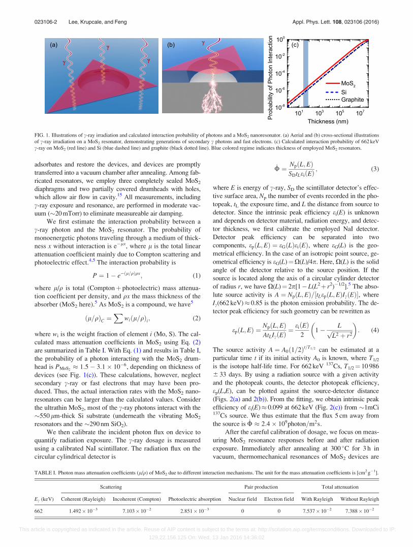
We first estimate the interaction probability between a
c-ray photon and the MoS2 resonator. The probability of
monoenergetic photons traveling through a medium of thick-
ness x without interaction is e�lx, where l is the total linear
attenuation coefficient mainly due to Compton scattering and
photoelectric effect.4,5 The interaction probability is
P ¼ 1� e�ðl=qÞqx; (1)
where l/q is total (Comptonþ photoelectric) mass attenua-
tion coefficient per density, and qx the mass thickness of the
absorber (MoS2 here).5 As MoS2 is a compound, we have5
ðl=qÞC ¼X
wiðl=qÞi; (2)
where wi is the weight fraction of element i (Mo, S). The cal-
culated mass attenuation coefficients in MoS2 using Eq. (2)
are summarized in Table I. With Eq. (1) and results in Table I,
the probability of a photon interacting with the MoS2 drum-
head is PMoS2� 1:5� 3:1� 10�6, depending on thickness of
devices (see Fig. 1(c)). These calculations, however, neglect
secondary c-ray or fast electrons that may have been pro-
duced. Thus, the actual interaction rates with the MoS2 nano-
resonators can be larger than the calculated values. Consider
the ultrathin MoS2, most of the c-ray photons interact with the
�550 lm-thick Si substrate (underneath the vibrating MoS2
resonators and the �290 nm SiO2).
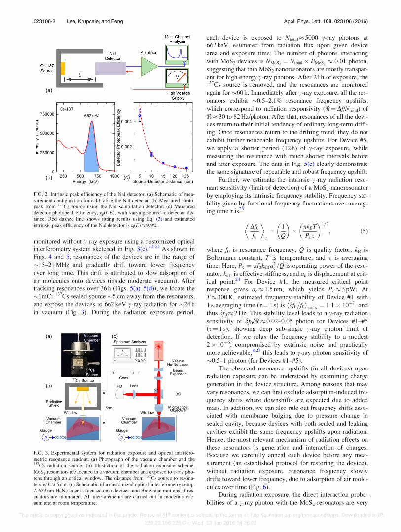
We then calibrate the incident photon flux on device to
quantify radiation exposure. The c-ray dosage is measured
using a calibrated NaI scintillator. The radiation flux on the
circular cylindrical detector is
_U ¼ Np L;Eð ÞSDtLei Eð Þ ; (3)
where E is energy of c-ray, SD the scintillator detector’s effec-
tive surface area, Np the number of events recorded in the pho-
topeak, tL the exposure time, and L the distance from source to
detector. Since the intrinsic peak efficiency ei(E) is unknown
and depends on detector material, radiation energy, and detec-
tor thickness, we first calibrate the employed NaI detector.
Detector peak efficiency can be separated into two
components, epðL;EÞ ¼ eGðLÞeiðEÞ, where eG(L) is the geo-
metrical efficiency. In the case of an isotropic point source, ge-
ometrical efficiency is eG(L)¼X(L)/4p. Here, X(L) is the solid
angle of the detector relative to the source position. If the
source is located along the axis of a circular cylinder detector
of radius r, we have X(L)¼ 2p[1�L(L2þ r2)�1/2].5 The abso-
lute source activity is A ¼ NpðL;EÞ=½tLepðL;EÞIcðEÞ�, where
Ic(662 keV)� 0.85 is the photon emission probability. The de-
tector peak efficiency for such geometry can be rewritten as
ep L;Eð Þ ¼ Np L;Eð ÞAtLIc Eð Þ ¼
ei Eð Þ2
1� LffiffiffiffiffiffiffiffiffiffiffiffiffiffiffiL2 þ r2p
� �: (4)
The source activity A ¼ A0ð1=2Þt=T1=2 can be estimated at a
particular time t if its initial activity A0 is known, where T1/2
is the isotope half-life time. For 662 keV 137Cs, T1/2¼ 10 986
6 33 days. By using a radiation source with a given activity
and the photopeak counts, the detector photopeak efficiency,
ep(L,E), can be plotted against the source-detector distance
(Figs. 2(a) and 2(b)). From the fitting, we obtain intrinsic peak
efficiency of ei(E)� 0.099 at 662 keV (Fig. 2(c)) from �1mCi137Cs source. We thus estimate that the flux 5 cm away from
the source is _U � 2:4� 109photon=m2s.
After the careful calibration of dosage, we focus on meas-
uring MoS2 resonance responses before and after radiation
exposure. Immediately after annealing at 300 �C for 3 h in
vacuum, thermomechanical resonances of MoS2 devices are
TABLE I. Photon mass attenuation coefficients (l/q) of MoS2 due to different interaction mechanisms. The unit for the mass attenuation coefficients is [cm2 g�1].
Ec (keV)
Scattering
Photoelectric absorption
Pair production Total attenuation
Coherent (Rayleigh) Incoherent (Compton) Nuclear field Electron field With Rayleigh Without Rayleigh
662 1.492� 10�3 7.103� 10�2 2.851� 10�3 0 0 7.537� 10�2 7.388� 10�2
FIG. 1. Illustrations of c-ray irradiation and calculated interaction probability of photons and a MoS2 nanoresonator. (a) Aerial and (b) cross-sectional illustrations
of c-ray irradiation on a MoS2 resonator, demonstrating generations of secondary c photons and fast electrons. (c) Calculated interaction probability of 662 keV
c-ray on MoS2 (red line) and Si (blue dashed line) and graphite (black dotted line). Blue colored regime indicates thickness of employed MoS2 resonators.
023106-2 Lee, Krupcale, and Feng Appl. Phys. Lett. 108, 023106 (2016)
This article is copyrighted as indicated in the article. Reuse of AIP content is subject to the terms at: http://scitation.aip.org/termsconditions. Downloaded to IP:
129.22.156.125 On: Wed, 13 Jan 2016 14:36:02
monitored without c-ray exposure using a customized optical
interferometry system sketched in Fig. 3(c).12,22 As shown in
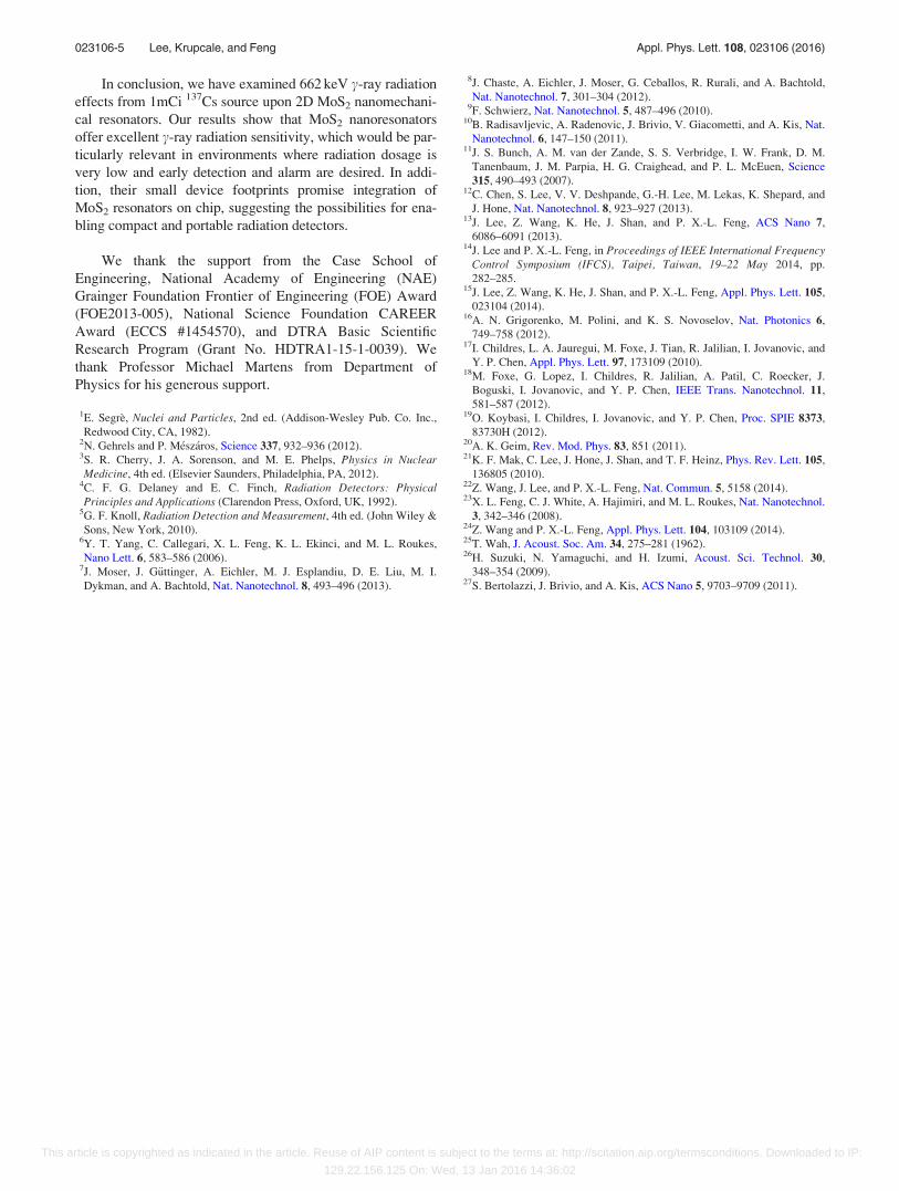
Figs. 4 and 5, resonances of the devices are in the range of
�15–21 MHz and gradually drift toward lower frequency
over long time. This drift is attributed to slow adsorption of
air molecules onto devices (inside moderate vacuum). After
tracking resonances over 36 h (Figs. 5(a)–5(d)), we locate the
�1mCi 137Cs sealed source �5 cm away from the resonators,
and expose the devices to 662 keV c-ray radiation for �24 h
in vacuum (Fig. 3). During the radiation exposure period,
each device is exposed to Ntotal� 5000 c-ray photons at
662 keV, estimated from radiation flux upon given device
area and exposure time. The number of photons interacting
with MoS2 devices is NMoS2¼ Ntotal � PMoS2
� 0:01 photon,
suggesting that thin MoS2 nanoresonators are mostly transpar-
ent for high energy c-ray photons. After 24 h of exposure, the137Cs source is removed, and the resonances are monitored
again for �60 h. Immediately after c-ray exposure, all the res-
onators exhibit �0.5–2.1% resonance frequency upshifts,
which correspond to radiation responsivity (<¼Df/Ntotal) of
<� 30 to 82 Hz/photon. After that, resonances of all the devi-
ces return to their initial tendency of ordinary long-term drift-
ing. Once resonances return to the drifting trend, they do not
exhibit further noticeable frequency upshifts. For Device #5,
we apply a shorter period (12 h) of c-ray exposure, while
measuring the resonance with much shorter intervals before
and after exposure. The data in Fig. 5(e) clearly demonstrate
the same signature of repeatable and robust frequency upshift.
Further, we estimate the intrinsic c-ray radiation reso-
nant sensitivity (limit of detection) of a MoS2 nanoresonator
by employing its intrinsic frequency stability. Frequency sta-
bility given by fractional frequency fluctuations over averag-
ing time s is23
�Df0
f0
�s
¼ 1
Q
� �� pkBT
Pcs
� �1=2
; (5)
where f0 is resonance frequency, Q is quality factor, kB is
Boltzmann constant, T is temperature, and s is averaging
time. Here, Pc ¼ pf0keffa2c=Q is operating power of the reso-
nator, keff is effective stiffness, and ac is displacement at crit-
ical point.24 For Device #1, the measured critical point
response gives ac� 1.5 nm, which yields Pc� 3 pW. At
T� 300 K, estimated frequency stability of Device #1 with
1 s averaging time (s¼ 1 s) is hdf0=f0is¼1s ¼ 1:1� 10�7, and
thus df0� 2 Hz. This stability level leads to a c-ray radiation
sensitivity of df0/<� 0.02–0.05 photon for Devices #1–#5
(s¼ 1 s), showing deep sub-single c-ray photon limit of
detection. If we relax the frequency stability to a modest
2� 10�6, compromised by extrinsic noise and practically
more achievable,8,23 this leads to c-ray photon sensitivity of
�0.5–1 photon (for Devices #1–#5).
The observed resonance upshifts (in all devices) upon
radiation exposure can be understood by examining charge
generation in the device structure. Among reasons that may
vary resonances, we can first exclude adsorption-induced fre-
quency shifts where downshifts are expected due to added
mass. In addition, we can also rule out frequency shifts asso-
ciated with membrane bulging due to pressure change in
sealed cavity, because devices with both sealed and leaking
cavities exhibit the same frequency upshifts upon radiation.
Hence, the most relevant mechanism of radiation effects on
these resonators is generation and interaction of charges.
Because we carefully anneal each device before any mea-
surement (an established protocol for restoring the device),
without radiation exposure, resonance frequency slowly
drifts toward lower frequency, due to adsorption of air mole-
cules over time (Fig. 6).
During radiation exposure, the direct interaction proba-
bilities of a c-ray photon with the MoS2 resonators are very
FIG. 3. Experimental system for radiation exposure and optical interfero-
metric resonance readout. (a) Photograph of the vacuum chamber and the137Cs radiation source. (b) Illustration of the radiation exposure scheme.
MoS2 resonators are located in a vacuum chamber and exposed to c-ray pho-
tons through an optical window. The distance from 137Cs source to resona-
tors is L� 5 cm. (c) Schematic of a customized optical interferometry setup.
A 633 nm HeNe laser is focused onto devices, and Brownian motions of res-
onators are monitored. All measurements are carried out in moderate vac-
uum and at room temperature.
FIG. 2. Intrinsic peak efficiency of the NaI detector. (a) Schematic of mea-
surement configuration for calibrating the NaI detector. (b) Measured photo-
peak from 137Cs source using the NaI scintillation detector. (c) Measured
detector photopeak efficiency, ep(L,E), with varying source-to-detector dis-
tance. Red dashed line shows fitting results using Eq. (3) and estimated
intrinsic peak efficiency of the NaI detector is ei(E)� 9.9%.
023106-3 Lee, Krupcale, and Feng Appl. Phys. Lett. 108, 023106 (2016)
This article is copyrighted as indicated in the article. Reuse of AIP content is subject to the terms at: http://scitation.aip.org/termsconditions. Downloaded to IP:
129.22.156.125 On: Wed, 13 Jan 2016 14:36:02
small, PMoS2� 1:5� 3:1� 10�6 (from Eqs. (1) and (2), Fig.
1(c)), because of the very thin devices, thus most c-ray pho-
tons first strike the much thicker SiO2/Si substrate under-
neath the vibrating MoS2, producing secondary c-ray
photons and fast electrons, which interact with the device
structure again and further create larger numbers of c pho-
tons and secondary electrons (SE) (Fig. 6(c)). These cascade
multi-interactions generate trapped charges in the device
structure across the SiO2 layer (Figs. 6(c) and 6(d)) and
cause electrostatic forces between the charged MoS2 drum-
head and the Si substrate, resulting in electrostatic tension
and deflection of the MoS2 drumheads (Fig. 6(d)), and the
resonance frequency upshifts. After exposure expires,
trapped charges are neutralized over time, so that the reso-
nance frequencies return to the initial frequency tendency
(Fig. 6(e)). We note that the quantitative details of the charg-
ing mechanism of c-ray interaction with the device structure
may depend on the work function of the Si substrate. It could
be interesting to alter and engineer the work function of the
substrate by depositing different metals of interest, or form-
ing metal silicides on the Si substrate, and investigate how
the device resonance changes with the work function.
Furthermore, we estimate the tension and deflection
induced in MoS2, based on the measured frequency upshifts.
The resonance frequency of clamped circular drumhead res-
onators in this study can be determined by25,26
f0 ¼1
2pk
d
2
� �16D
qtd4k
d
2
� �2
þ rtd2
4D
" # !1=2
; (6)
where d is the diameter, t the thickness, D¼EYt3/[12(1� �2)]
the bending rigidity, r the tension [N/m2], EY the Young’s
modulus, q the density, and � the Poisson’s ratio of MoS2,
and k is the mode parameter determined numerically.26
Extracted Young’s modulus of MoS2 from the resonances
data is 0.2–0.4 TPa, showing good agreement with the previ-
ously reported values.13,27 For further analysis, we employ
Device #1 which particularly does not consist of structural
defects (e.g., thickness variation or holes) for modeling.
The initial surface tension on MoS2 resonators is �0.1 N/m
(6.84 ppm of strain).13 Upon c-ray exposure, the resonance
frequency of Device #1 shifts from �19.375 MHz to
�19.784 MHz, which yields a tension level of �0.240 N/m
(16.41 ppm of strain), corresponding to �12 nm static dis-
placement at the center of the diaphragm.
FIG. 6. Illustrations of c-ray radiation effects on a MoS2 resonator. (a) Clean
MoS2 resonator right after annealing. (b) Air molecules adsorbing on device
surface. (c) c-ray irradiation onto device, generating secondary c-ray photons
and fast electrons. (d) c-ray irradiation described in (c) produces trapped
charges, which causes electrostatic forces, tension, and deformation of the
MoS2 resonator. (e) Generated trapped charges are neutralized over time af-
ter radiation expires.
FIG. 4. Measured undriven thermomechanical resonances from MoS2 drum-
head resonators. (a)–(d) Measured resonances immediately after annealing
from Device #1 (d� 5.4 lm, t� 31 nm), Device #2 (d� 5.5 lm, t� 51 nm),
Device #3 (d� 5.6 lm, t� 55 nm), and Device #4 (d� 6.1 lm, t� 81 nm),
respectively. Device #4 has a small opening, which acts as a leaking aper-
ture. Red dashed lines show fitting results using a finite-Q harmonic resona-
tor model. Insets show optical images of devices. All scale bars are 5 lm.
FIG. 5. Measured resonance frequencies versus time before and after c-ray
radiation exposure. (a)–(d) Measured frequency evolution from Device #1,
Device #2, Device #3, and Device #4, respectively. Each of the resonators is
exposed for �24 h (light blue region). (e) Data from Device #5 with �12 h
of exposure and much shorter measurement intervals. Insets show optical
images of the individual MoS2 resonators. All scale bars are 3 lm.
023106-4 Lee, Krupcale, and Feng Appl. Phys. Lett. 108, 023106 (2016)
This article is copyrighted as indicated in the article. Reuse of AIP content is subject to the terms at: http://scitation.aip.org/termsconditions. Downloaded to IP:
129.22.156.125 On: Wed, 13 Jan 2016 14:36:02
In conclusion, we have examined 662 keV c-ray radiation
effects from 1mCi 137Cs source upon 2D MoS2 nanomechani-
cal resonators. Our results show that MoS2 nanoresonators
offer excellent c-ray radiation sensitivity, which would be par-
ticularly relevant in environments where radiation dosage is
very low and early detection and alarm are desired. In addi-
tion, their small device footprints promise integration of
MoS2 resonators on chip, suggesting the possibilities for ena-
bling compact and portable radiation detectors.
We thank the support from the Case School of
Engineering, National Academy of Engineering (NAE)
Grainger Foundation Frontier of Engineering (FOE) Award
(FOE2013-005), National Science Foundation CAREER
Award (ECCS #1454570), and DTRA Basic Scientific
Research Program (Grant No. HDTRA1-15-1-0039). We
thank Professor Michael Martens from Department of
Physics for his generous support.
1E. Segre, Nuclei and Particles, 2nd ed. (Addison-Wesley Pub. Co. Inc.,
Redwood City, CA, 1982).2N. Gehrels and P. M�esz�aros, Science 337, 932–936 (2012).3S. R. Cherry, J. A. Sorenson, and M. E. Phelps, Physics in NuclearMedicine, 4th ed. (Elsevier Saunders, Philadelphia, PA, 2012).
4C. F. G. Delaney and E. C. Finch, Radiation Detectors: PhysicalPrinciples and Applications (Clarendon Press, Oxford, UK, 1992).
5G. F. Knoll, Radiation Detection and Measurement, 4th ed. (John Wiley &
Sons, New York, 2010).6Y. T. Yang, C. Callegari, X. L. Feng, K. L. Ekinci, and M. L. Roukes,
Nano Lett. 6, 583–586 (2006).7J. Moser, J. G€uttinger, A. Eichler, M. J. Esplandiu, D. E. Liu, M. I.
Dykman, and A. Bachtold, Nat. Nanotechnol. 8, 493–496 (2013).
8J. Chaste, A. Eichler, J. Moser, G. Ceballos, R. Rurali, and A. Bachtold,
Nat. Nanotechnol. 7, 301–304 (2012).9F. Schwierz, Nat. Nanotechnol. 5, 487–496 (2010).
10B. Radisavljevic, A. Radenovic, J. Brivio, V. Giacometti, and A. Kis, Nat.
Nanotechnol. 6, 147–150 (2011).11J. S. Bunch, A. M. van der Zande, S. S. Verbridge, I. W. Frank, D. M.
Tanenbaum, J. M. Parpia, H. G. Craighead, and P. L. McEuen, Science
315, 490–493 (2007).12C. Chen, S. Lee, V. V. Deshpande, G.-H. Lee, M. Lekas, K. Shepard, and
J. Hone, Nat. Nanotechnol. 8, 923–927 (2013).13J. Lee, Z. Wang, K. He, J. Shan, and P. X.-L. Feng, ACS Nano 7,
6086–6091 (2013).14J. Lee and P. X.-L. Feng, in Proceedings of IEEE International Frequency
Control Symposium (IFCS), Taipei, Taiwan, 19–22 May 2014, pp.
282–285.15J. Lee, Z. Wang, K. He, J. Shan, and P. X.-L. Feng, Appl. Phys. Lett. 105,
023104 (2014).16A. N. Grigorenko, M. Polini, and K. S. Novoselov, Nat. Photonics 6,
749–758 (2012).17I. Childres, L. A. Jauregui, M. Foxe, J. Tian, R. Jalilian, I. Jovanovic, and
Y. P. Chen, Appl. Phys. Lett. 97, 173109 (2010).18M. Foxe, G. Lopez, I. Childres, R. Jalilian, A. Patil, C. Roecker, J.
Boguski, I. Jovanovic, and Y. P. Chen, IEEE Trans. Nanotechnol. 11,
581–587 (2012).19O. Koybasi, I. Childres, I. Jovanovic, and Y. P. Chen, Proc. SPIE 8373,
83730H (2012).20A. K. Geim, Rev. Mod. Phys. 83, 851 (2011).21K. F. Mak, C. Lee, J. Hone, J. Shan, and T. F. Heinz, Phys. Rev. Lett. 105,
136805 (2010).22Z. Wang, J. Lee, and P. X.-L. Feng, Nat. Commun. 5, 5158 (2014).23X. L. Feng, C. J. White, A. Hajimiri, and M. L. Roukes, Nat. Nanotechnol.
3, 342–346 (2008).24Z. Wang and P. X.-L. Feng, Appl. Phys. Lett. 104, 103109 (2014).25T. Wah, J. Acoust. Soc. Am. 34, 275–281 (1962).26H. Suzuki, N. Yamaguchi, and H. Izumi, Acoust. Sci. Technol. 30,
348–354 (2009).27S. Bertolazzi, J. Brivio, and A. Kis, ACS Nano 5, 9703–9709 (2011).
023106-5 Lee, Krupcale, and Feng Appl. Phys. Lett. 108, 023106 (2016)
This article is copyrighted as indicated in the article. Reuse of AIP content is subject to the terms at: http://scitation.aip.org/termsconditions. Downloaded to IP:
129.22.156.125 On: Wed, 13 Jan 2016 14:36:02