L. Hart, James Nathaniel, Mitra L. Taheri, Fan Ren, S. J ...
Effects of fluorine incorporation into β-Ga2O3Jiangcheng Yang, Chaker Fares, F. Ren, Ribhu Sharma, Erin Patrick, Mark E. Law, S. J. Pearton, and AkitoKuramata
Citation: Journal of Applied Physics 123, 165706 (2018); doi: 10.1063/1.5031001View online: https://doi.org/10.1063/1.5031001View Table of Contents: http://aip.scitation.org/toc/jap/123/16Published by the American Institute of Physics
Effects of fluorine incorporation into b-Ga2O3
Jiangcheng Yang,1 Chaker Fares,1 F. Ren,1 Ribhu Sharma,2 Erin Patrick,3 Mark E. Law,3
S. J. Pearton,2 and Akito Kuramata4
1Department of Chemical Engineering, University of Florida, Gainesville, Florida 32611, USA2Department of Materials Science and Engineering, University of Florida, Gainesville, Florida 32611, USA3Department of Electrical Engineering, University of Florida, Gainesville, Florida 32611, USA4Tamura Corporation and Novel Crystal Technology, Inc., Sayama, Saitama 350-1328, Japan
(Received 27 March 2018; accepted 12 April 2018; published online 30 April 2018)
b-Ga2O3 rectifiers fabricated on lightly doped epitaxial layers on bulk substrates were exposed to
CF4 plasmas. This produced a significant decrease in Schottky barrier height relative to unexposed
control diodes (0.68 eV compared to 1.22 eV) and degradation in ideality factor (2.95 versus 1.01
for the control diodes). High levels of F (>1022 cm�3) were detected in the near-surface region by
Secondary Ion Mass Spectrometry. The diffusion of fluorine into the Ga2O3 was thermally acti-
vated with an activation energy of 1.24 eV. Subsequent annealing in the range 350–400 �C brought
recovery of the diode characteristics and an increase in barrier height to a value larger than in the
unexposed control diodes (1.36 eV). Approximately 70% of the initial F was removed from the
Ga2O3 by 400 �C, with the surface outgas rate also being thermally activated with an activation
energy of 1.23 eV. Very good fits to the experimental data were obtained by integrating physics
of the outdiffusion mechanisms into the Florida Object Oriented Process Simulator code and
assuming that the outgas rate from the surface was mediated through fluorine molecule formation.
The fluorine molecule forward reaction rate had an activation energy of 1.24 eV, while the reversal
rate of this reaction had an activation energy of 0.34 eV. The net carrier density in the drift region
of the rectifiers decreased after CF4 exposure and annealing at 400 �C. The data are consistent with
a model in which near-surface plasma-induced damage creates degraded Schottky barrier charac-
teristics, but as the samples are annealed, this damage is removed, leaving the compensation effect
of Si donors by F� ions. The barrier lowering and then enhancement are due to the interplay
between surface defects and the chemical effects of the fluorine. Published by AIP Publishing.https://doi.org/10.1063/1.5031001
INTRODUCTION
The role of fluorine in compound semiconductors has
been of interest since the initial observations of partially
reversible changes in the two dimensional electron gas
(2DEG) concentration (NS) in AlInAs/InGaAs modulation-
doped structures upon thermal annealing at low temperatures
(280 �C).1–4 A number of experiments involving Hall mea-
surements of SiNx-passivated versus capless samples,
together with chemical profiling of impurities in the near-
surface region, established that the recovery of NS was asso-
ciated with the outdiffusion of fluorine atoms from the
Si-doped n-type InAlAs layer.2,3 The thermally activated dif-
fusion of fluorine into the Si-doped AlInAs layer was found
to be the main cause of the reduction in carrier density, and
subsequent annealing could effectively recover the original
NS values.1–4 This effect has been used to control the thresh-
old voltage in both AlInAs and AlGaN/GaN High Electron
Mobility Transistors (HEMTs) through compensating Si
donors with the negatively charged F ions.5–8 The fluorine
can be incorporated during exposure to wet chemical solu-
tions such as HF, by direct implantation of low energy fluo-
rine ions or by immersion in a fluorine-containing plasma.
The fluorine atoms are strongly electronegative and become
negatively charged, effectively raising the potential in the
AlGaN or AlInAs barrier and therefore in the 2DEG channel.
As a result, the HEMT threshold voltage can be shifted to
positive values, and enhancement mode devices can be
fabricated.
Recent results have postulated that similar effects may
occur in Ga2O3 rectifiers, in which larger-than-expected
effective barrier heights of 1.46 eV for Pt (compared to
1.16 eV in reference samples) were obtained for samples
exposed to hydrofluoric acid prior to metal deposition.9 The
results were consistent with F atoms acting as negative ions
and compensating the ionized Si donors in the Ga2O3 to form
neutral complexes, leading to additional surface depletion.9
However, no direct confirmation of the presence of fluorine
was made, nor any details of the thermal stability of the
effect. Since Ga2O3 is attracting significant recent attention
for use in high power electronics and solar blind UV photode-
tectors,10–26 there is a need to more fully understand the
effects of unintentionally incorporated impurities such as
fluorine and hydrogen, both of which may have strong effects
on the doping in the near-surface region.27–29 There are few
effective wet etchants for Ga2O3 and patterning of this mate-
rial is typically done by dry etching methods.30–33 This means
that post-etch residues are usually removed with acid and sol-
vent solutions and that the Ga2O3 surface is additionally
exposed to such solutions during patterning of dielectrics.
In this paper, we show that high concentrations of fluo-
rine are incorporated into the near-surface region of Ga2O3
0021-8979/2018/123(16)/165706/7/$30.00 Published by AIP Publishing.123, 165706-1
JOURNAL OF APPLIED PHYSICS 123, 165706 (2018)
during exposure to CF4 plasmas and that it remains in the
material to temperatures beyond 400 �C. We use Schottky
rectifier structures to elucidate the mechanisms of barrier
lowering and subsequent enhancement during plasma expo-
sure and annealing to remove plasma damage. Our previous
plasma damage work showed barrier lowering for such surfa-
ces, as evidenced by the increased forward and reverse leak-
age in diodes fabricated on those surfaces.32,33 A post-gate
annealing at a gate electrode- compatible temperature of
400 �C proved to be effective in recovering the initial
plasma-induced damage. Once this damage was annealed,
the gate leakage current at reverse bias was decreased by one
to two orders of magnitude. This is also consistent with the
temperatures at which point defect damage in Ga2O3 is
observed to anneal out.34,35 The barrier height was also
increased relative to control samples not exposed to fluorine,
showing that compensation of Si donors by F� ions occurs in
Ga2O3. The dominant mechanisms for the outdiffusion kinet-
ics were extracted from simulations using the Florida Object
Oriented Process Simulator (FLOOPS) code.
EXPERIMENTAL
The starting material consisted of vertical structures of
epitaxial layers (7 lm final thickness) of lightly Si-doped n-
type (5.2� 1016 cm�3) Ga2O3 grown by Hydride Vapor
Phase Epitaxy (HVPE) on nþ bulk, b-phase Sn-doped Ga2O3
single crystal wafers (�650 lm thick) with (001) surface
orientation (Tamura Corporation, Japan). The source gases
used were GaCl and O2 transported by a N2 carrier gas. GaCl
was generated in the upstream region of the reactor by the
reaction between high-purity Ga metal (6N grade) and chlo-
rine (Cl2) gas at 850 �C. GaCl and O2 were separately intro-
duced to the downstream region (growth zone) where the
b-Ga2O3 substrate was placed on a quartz glass susceptor.
The growth zone was heated to a temperature between 800
and 1050 �C under a flow of N2 containing O2 at a partial
pressure of 2.5� 10�3 atm. The b-Ga2O3 layer was subse-
quently grown by supplying GaCl with an input partial pres-
sure of 5.0� 10�4 atm with a fixed input VI/III (2O2/GaCl)
ratio of 10. The total gas flow rate was 1600 sccm throughout
the entire growth process. The substrates were grown by the
edge-defined film-fed method. These substrates had carrier
concentration of 3.6� 1018 cm�3 as obtained from Hall mea-
surements. The dislocation density from etch pit observation
was of the order of 103 cm�2, and the x-ray diffraction full-
width-half maximum was 137 arc sec. The HVPE layers
were treated by chemical mechanical planarization to
remove pits, as described previously and the back surface of
the substrate was also polished to remove sub-surface dam-
age and enhance Ohmic contact formation.
Diodes were fabricated by depositing full area back
Ohmic contacts of Ti/Au (20 nm/80 nm) by E-beam evapora-
tion and annealed in an SSI Solaris 150 rapid thermal anneal-
ing (RTA) system at 550 �C for 30 s under nitrogen ambient.
A 100 nm of SiNx film was deposited onto the sample sur-
face with a plasma enhanced chemical vapor deposition sys-
tem at 300 �C using silane and ammonia. Prior to the film
deposition, the sample surface was treated with ozone for
10 min to remove any carbon contaminations. The SiNx
contact windows were patterned with standard lithography
process and opened with Technics reactive ion etching (RIE)
system with CF4 plasma [150 mTorr (20 Pa), CF4 flow rate
of 30 sccm, and 50 W power]. The sample was then exposed
in CF4 plasma for additional 5 min after the opening of these
SiNx windows. We also made reference samples with no
plasma exposure and samples exposed to Ar plasma under
the same power and time conditions to simulate the effect of
plasma damage, but not chemical effect of fluorine. The front
side Schottky contacts were overlapped 5 lm on the SiNx
window opening and formed by standard lift-off of E-beam
deposited Ni/Au (20 nm/150 nm). The size of these contacts
was 40 lm� 40 lm. The CF4 exposed samples were diced
into pieces and annealed at 350 and 400 �C for 10 min under
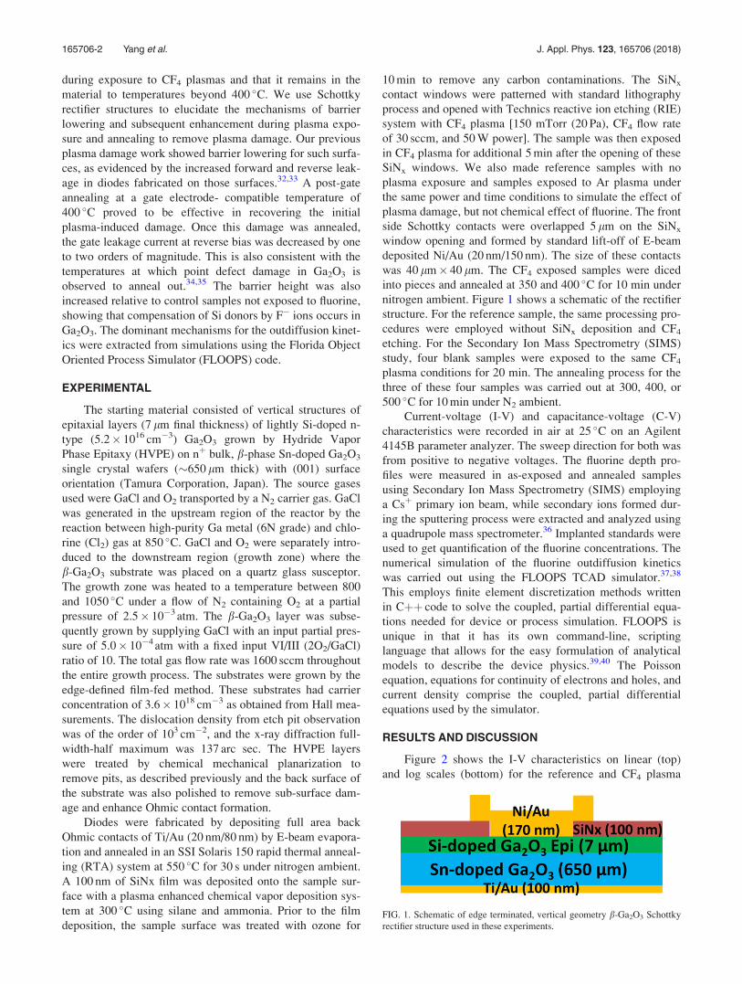
nitrogen ambient. Figure 1 shows a schematic of the rectifier
structure. For the reference sample, the same processing pro-
cedures were employed without SiNx deposition and CF4
etching. For the Secondary Ion Mass Spectrometry (SIMS)
study, four blank samples were exposed to the same CF4
plasma conditions for 20 min. The annealing process for the
three of these four samples was carried out at 300, 400, or
500 �C for 10 min under N2 ambient.
Current-voltage (I-V) and capacitance-voltage (C-V)
characteristics were recorded in air at 25 �C on an Agilent
4145B parameter analyzer. The sweep direction for both was
from positive to negative voltages. The fluorine depth pro-
files were measured in as-exposed and annealed samples
using Secondary Ion Mass Spectrometry (SIMS) employing
a Csþ primary ion beam, while secondary ions formed dur-
ing the sputtering process were extracted and analyzed using
a quadrupole mass spectrometer.36 Implanted standards were
used to get quantification of the fluorine concentrations. The
numerical simulation of the fluorine outdiffusion kinetics
was carried out using the FLOOPS TCAD simulator.37,38
This employs finite element discretization methods written
in Cþþ code to solve the coupled, partial differential equa-
tions needed for device or process simulation. FLOOPS is
unique in that it has its own command-line, scripting
language that allows for the easy formulation of analytical
models to describe the device physics.39,40 The Poisson
equation, equations for continuity of electrons and holes, and
current density comprise the coupled, partial differential
equations used by the simulator.
RESULTS AND DISCUSSION
Figure 2 shows the I-V characteristics on linear (top)
and log scales (bottom) for the reference and CF4 plasma
FIG. 1. Schematic of edge terminated, vertical geometry b-Ga2O3 Schottky
rectifier structure used in these experiments.
165706-2 Yang et al. J. Appl. Phys. 123, 165706 (2018)
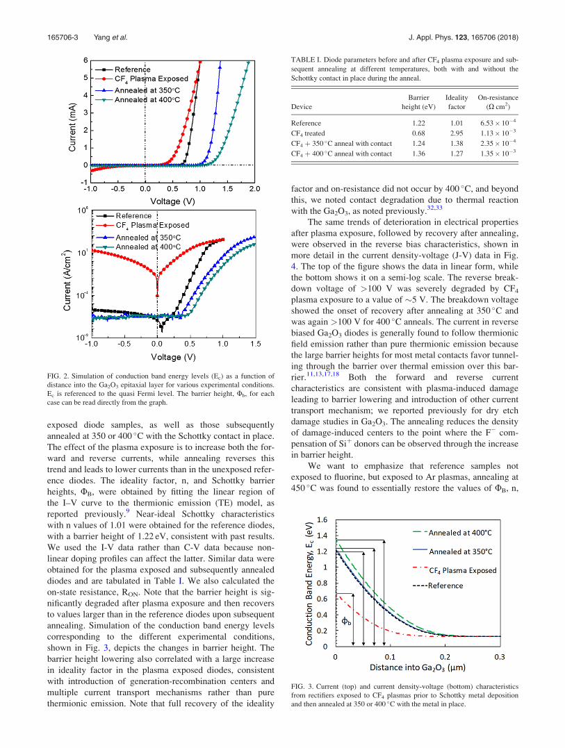
exposed diode samples, as well as those subsequently
annealed at 350 or 400 �C with the Schottky contact in place.
The effect of the plasma exposure is to increase both the for-
ward and reverse currents, while annealing reverses this
trend and leads to lower currents than in the unexposed refer-
ence diodes. The ideality factor, n, and Schottky barrier
heights, UB, were obtained by fitting the linear region of
the I–V curve to the thermionic emission (TE) model, as
reported previously.9 Near-ideal Schottky characteristics
with n values of 1.01 were obtained for the reference diodes,
with a barrier height of 1.22 eV, consistent with past results.
We used the I-V data rather than C-V data because non-
linear doping profiles can affect the latter. Similar data were
obtained for the plasma exposed and subsequently annealed
diodes and are tabulated in Table I. We also calculated the
on-state resistance, RON. Note that the barrier height is sig-
nificantly degraded after plasma exposure and then recovers
to values larger than in the reference diodes upon subsequent
annealing. Simulation of the conduction band energy levels
corresponding to the different experimental conditions,
shown in Fig. 3, depicts the changes in barrier height. The
barrier height lowering also correlated with a large increase
in ideality factor in the plasma exposed diodes, consistent
with introduction of generation-recombination centers and
multiple current transport mechanisms rather than pure
thermionic emission. Note that full recovery of the ideality
factor and on-resistance did not occur by 400 �C, and beyond
this, we noted contact degradation due to thermal reaction
with the Ga2O3, as noted previously.32,33
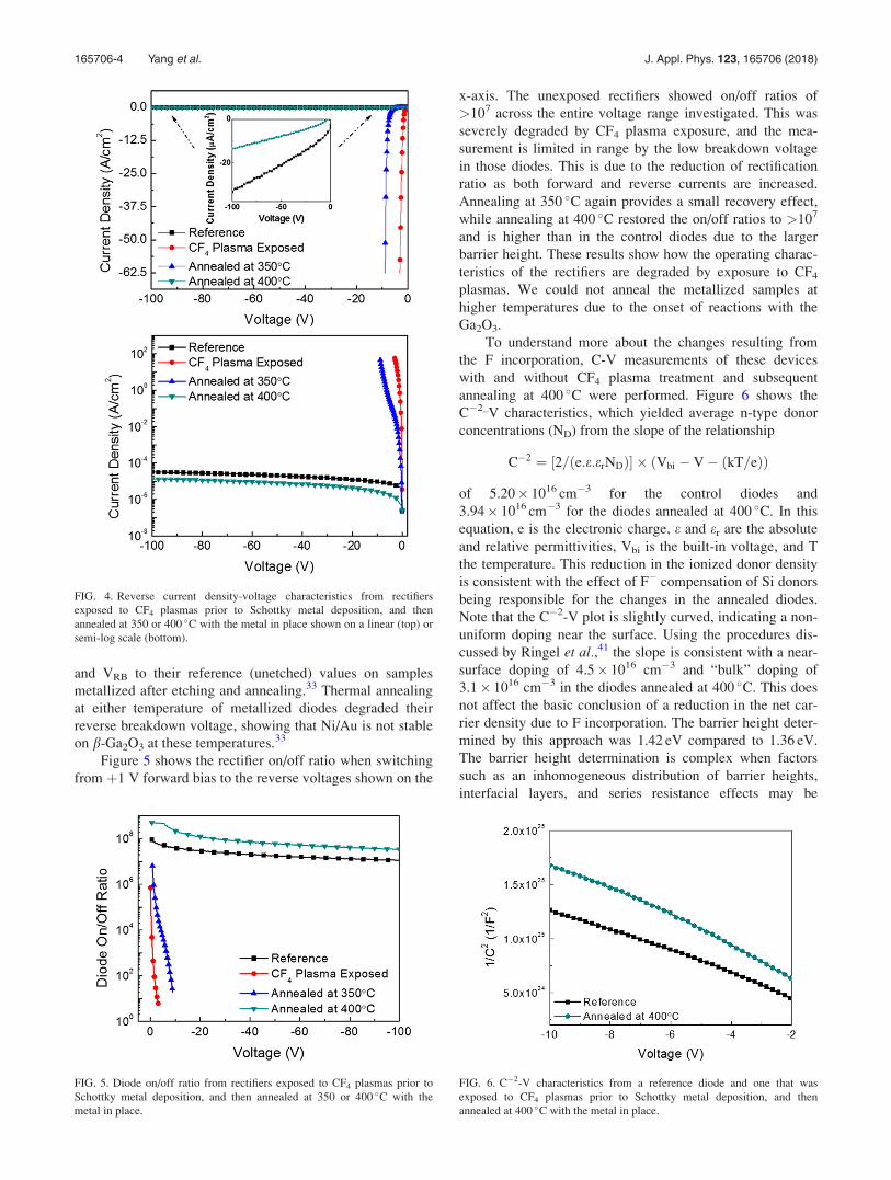
The same trends of deterioration in electrical properties
after plasma exposure, followed by recovery after annealing,
were observed in the reverse bias characteristics, shown in
more detail in the current density-voltage (J-V) data in Fig.
4. The top of the figure shows the data in linear form, while
the bottom shows it on a semi-log scale. The reverse break-
down voltage of >100 V was severely degraded by CF4
plasma exposure to a value of �5 V. The breakdown voltage
showed the onset of recovery after annealing at 350 �C and
was again >100 V for 400 �C anneals. The current in reverse
biased Ga2O3 diodes is generally found to follow thermionic
field emission rather than pure thermionic emission because
the large barrier heights for most metal contacts favor tunnel-
ing through the barrier over thermal emission over this bar-
rier.11,13,17,18 Both the forward and reverse current
characteristics are consistent with plasma-induced damage
leading to barrier lowering and introduction of other current
transport mechanism; we reported previously for dry etch
damage studies in Ga2O3. The annealing reduces the density
of damage-induced centers to the point where the F� com-
pensation of Siþ donors can be observed through the increase
in barrier height.
We want to emphasize that reference samples not
exposed to fluorine, but exposed to Ar plasmas, annealing at
450 �C was found to essentially restore the values of UB, n,
FIG. 2. Simulation of conduction band energy levels (Ec) as a function of
distance into the Ga2O3 epitaxial layer for various experimental conditions.
Ec is referenced to the quasi Fermi level. The barrier height, Ub, for each
case can be read directly from the graph.
TABLE I. Diode parameters before and after CF4 plasma exposure and sub-
sequent annealing at different temperatures, both with and without the
Schottky contact in place during the anneal.
Device
Barrier
height (eV)
Ideality
factor
On-resistance
(X cm2)
Reference 1.22 1.01 6.53� 10�4
CF4 treated 0.68 2.95 1.13� 10�3
CF4 þ 350 �C anneal with contact 1.24 1.38 2.35� 10�4
CF4 þ 400 �C anneal with contact 1.36 1.27 1.35� 10�3
FIG. 3. Current (top) and current density-voltage (bottom) characteristics
from rectifiers exposed to CF4 plasmas prior to Schottky metal deposition
and then annealed at 350 or 400 �C with the metal in place.
165706-3 Yang et al. J. Appl. Phys. 123, 165706 (2018)
and VRB to their reference (unetched) values on samples
metallized after etching and annealing.33 Thermal annealing
at either temperature of metallized diodes degraded their
reverse breakdown voltage, showing that Ni/Au is not stable
on b-Ga2O3 at these temperatures.33
Figure 5 shows the rectifier on/off ratio when switching
from þ1 V forward bias to the reverse voltages shown on the
x-axis. The unexposed rectifiers showed on/off ratios of
>107 across the entire voltage range investigated. This was
severely degraded by CF4 plasma exposure, and the mea-
surement is limited in range by the low breakdown voltage
in those diodes. This is due to the reduction of rectification
ratio as both forward and reverse currents are increased.
Annealing at 350 �C again provides a small recovery effect,
while annealing at 400 �C restored the on/off ratios to >107
and is higher than in the control diodes due to the larger
barrier height. These results show how the operating charac-
teristics of the rectifiers are degraded by exposure to CF4
plasmas. We could not anneal the metallized samples at
higher temperatures due to the onset of reactions with the
Ga2O3.
To understand more about the changes resulting from
the F incorporation, C-V measurements of these devices
with and without CF4 plasma treatment and subsequent
annealing at 400 �C were performed. Figure 6 shows the
C�2_V characteristics, which yielded average n-type donor
concentrations (ND) from the slope of the relationship
C�2 ¼ 2= e:e:erNDð Þ½ � � Vbi � V� kT=eð Þð Þ
of 5.20� 1016 cm�3 for the control diodes and
3.94� 1016 cm�3 for the diodes annealed at 400 �C. In this
equation, e is the electronic charge, e and er are the absolute
and relative permittivities, Vbi is the built-in voltage, and T
the temperature. This reduction in the ionized donor density
is consistent with the effect of F� compensation of Si donors
being responsible for the changes in the annealed diodes.
Note that the C�2-V plot is slightly curved, indicating a non-
uniform doping near the surface. Using the procedures dis-
cussed by Ringel et al.,41 the slope is consistent with a near-
surface doping of 4.5� 1016 cm�3 and “bulk” doping of
3.1� 1016 cm�3 in the diodes annealed at 400 �C. This does
not affect the basic conclusion of a reduction in the net car-
rier density due to F incorporation. The barrier height deter-
mined by this approach was 1.42 eV compared to 1.36 eV.
The barrier height determination is complex when factors
such as an inhomogeneous distribution of barrier heights,
interfacial layers, and series resistance effects may be
FIG. 4. Reverse current density-voltage characteristics from rectifiers
exposed to CF4 plasmas prior to Schottky metal deposition, and then
annealed at 350 or 400 �C with the metal in place shown on a linear (top) or
semi-log scale (bottom).
FIG. 5. Diode on/off ratio from rectifiers exposed to CF4 plasmas prior to
Schottky metal deposition, and then annealed at 350 or 400 �C with the
metal in place.
FIG. 6. C�2-V characteristics from a reference diode and one that was
exposed to CF4 plasmas prior to Schottky metal deposition, and then
annealed at 400 �C with the metal in place.
165706-4 Yang et al. J. Appl. Phys. 123, 165706 (2018)
present. To allow a consistent comparison of the effects of F,
we used the I-V data.
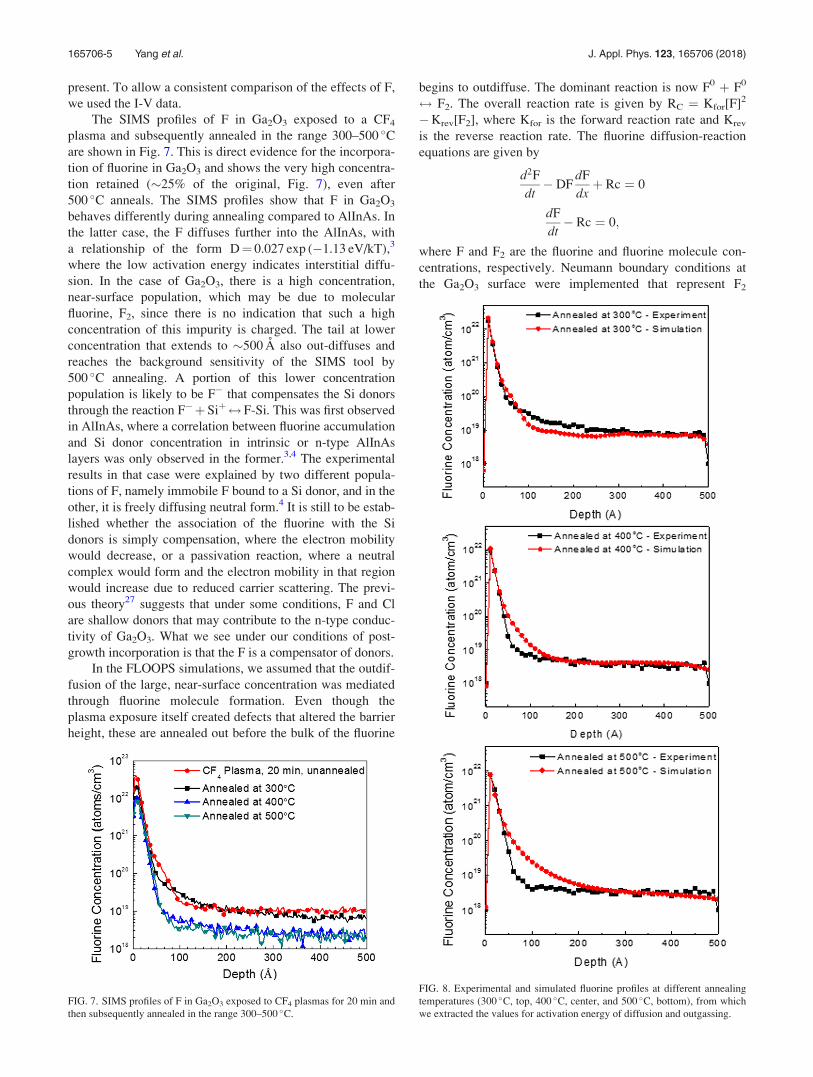
The SIMS profiles of F in Ga2O3 exposed to a CF4
plasma and subsequently annealed in the range 300–500 �Care shown in Fig. 7. This is direct evidence for the incorpora-
tion of fluorine in Ga2O3 and shows the very high concentra-
tion retained (�25% of the original, Fig. 7), even after
500 �C anneals. The SIMS profiles show that F in Ga2O3
behaves differently during annealing compared to AlInAs. In
the latter case, the F diffuses further into the AlInAs, with
a relationship of the form D¼ 0.027 exp (�1.13 eV/kT),3
where the low activation energy indicates interstitial diffu-
sion. In the case of Ga2O3, there is a high concentration,
near-surface population, which may be due to molecular
fluorine, F2, since there is no indication that such a high
concentration of this impurity is charged. The tail at lower
concentration that extends to �500 A also out-diffuses and
reaches the background sensitivity of the SIMS tool by
500 �C annealing. A portion of this lower concentration
population is likely to be F� that compensates the Si donors
through the reaction F�þ Siþ$ F-Si. This was first observed
in AlInAs, where a correlation between fluorine accumulation
and Si donor concentration in intrinsic or n-type AlInAs
layers was only observed in the former.3,4 The experimental
results in that case were explained by two different popula-
tions of F, namely immobile F bound to a Si donor, and in the
other, it is freely diffusing neutral form.4 It is still to be estab-
lished whether the association of the fluorine with the Si
donors is simply compensation, where the electron mobility
would decrease, or a passivation reaction, where a neutral
complex would form and the electron mobility in that region
would increase due to reduced carrier scattering. The previ-
ous theory27 suggests that under some conditions, F and Cl
are shallow donors that may contribute to the n-type conduc-
tivity of Ga2O3. What we see under our conditions of post-
growth incorporation is that the F is a compensator of donors.
In the FLOOPS simulations, we assumed that the outdif-
fusion of the large, near-surface concentration was mediated
through fluorine molecule formation. Even though the
plasma exposure itself created defects that altered the barrier
height, these are annealed out before the bulk of the fluorine
begins to outdiffuse. The dominant reaction is now F0 þ F0
$ F2. The overall reaction rate is given by RC ¼ Kfor[F]2
�Krev[F2], where Kfor is the forward reaction rate and Krev
is the reverse reaction rate. The fluorine diffusion-reaction
equations are given by
d2F
dt� DF
dF
dxþ Rc ¼ 0
dF
dt� Rc ¼ 0;
where F and F2 are the fluorine and fluorine molecule con-
centrations, respectively. Neumann boundary conditions at
the Ga2O3 surface were implemented that represent F2
FIG. 7. SIMS profiles of F in Ga2O3 exposed to CF4 plasmas for 20 min and
then subsequently annealed in the range 300–500 �C.
FIG. 8. Experimental and simulated fluorine profiles at different annealing
temperatures (300 �C, top, 400 �C, center, and 500 �C, bottom), from which
we extracted the values for activation energy of diffusion and outgassing.
165706-5 Yang et al. J. Appl. Phys. 123, 165706 (2018)
outgassing with flux equal to: KS � F; where KS is the sur-
face outgas rate of F and was tuned to fit the experimental
data. Examples of the fitted data are shown in Fig. 8 for the
samples annealed at 300, 400, and 500 �C. The activation
energy for diffusion was obtained by fitting the experimental
data at the different annealing temperatures, as shown in Fig.
9 (top), with a value of 1.23 eV. The forward and reverse
reaction rates, Kfor, Krev, were also tuned to fit the data and
followed Arrhenius dependence with temperature, as shown
in Fig. 9 (bottom). The respective values of these parameters
were 1.24 and 0.34 eV, respectively.
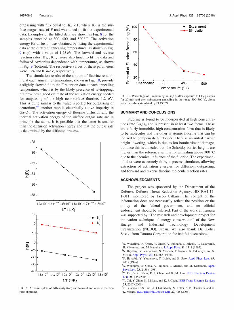
The simulation results of the amount of fluorine remain-
ing at each annealing temperature, shown in Fig. 10, provide
a slightly skewed fit to the F retention data at each annealing
temperature, which is by the likely presence of re-trapping,
but provides a good estimate of the activation energy needed
for outgassing of the high near-surface fluorine, 1.24 eV.
This is quite similar to the value reported for outgassing of
deuterium,40 another mobile electrically active impurity in
Ga2O3. The activation energy of fluorine diffusion and the
thermal activation energy of the surface outgas rate are in
principle the same. It is possible that the latter is smaller
than the diffusion activation energy and that the outgas rate
is determined by the diffusion process.
SUMMARY AND CONCLUSIONS
Fluorine is found to be incorporated at high concentra-
tions into Ga2O3 and is present in at least two forms. These
are a fairly immobile, high concentration form that is likely
to be molecules and the other is atomic fluorine that can be
ionized to compensate Si donors. There is an initial barrier
height lowering, which is due to ion bombardment damage,
but once this is annealed out, the Schottky barrier heights are
higher than the reference sample for annealing above 300 �Cdue to the chemical influence of the fluorine. The experimen-
tal data were accurately fit by a process simulator, allowing
extraction of activation energies for diffusion, outgassing,
and forward and reverse fluorine molecule reaction rates.
ACKNOWLEDGMENTS
The project was sponsored by the Department of the
Defense, Defense Threat Reduction Agency, HDTRA1-17-
1-011, monitored by Jacob Calkins. The content of the
information does not necessarily reflect the position or the
policy of the federal government, and no official
endorsement should be inferred. Part of the work at Tamura
was supported by “The research and development project for
innovation technique of energy conservation” of the New
Energy and Industrial Technology Development
Organization (NEDO), Japan. We also thank Dr. Kohei
Sasaki from Tamura Corporation for fruitful discussions.
1A. Wakejima, K. Onda, Y. Ando, A. Fujihara, E. Mizuki, T. Nakayama,
H. Miyamoto, and M. Kuzuhara, J. Appl. Phys. 81, 1311 (1997).2N. Hayafuji, Y. Yamamoto, N. Yoshida, T. Sonoda, S. Takamiya, and S.
Mitsui, Appl. Phys. Lett. 66, 863 (1995).3N. Hayafuji, Y. Yamamoto, T. Ishida, and K. Sato, Appl. Phys. Lett. 69,
4075 (1996).4A. Wakejima, K. Onda, A. Fujihara, E. Mizuki, and M. Kanamori, Appl.
Phys. Lett. 73, 2459 (1998).5Y. Cai, Y. G. Zhou, K. J. Chen, and K. M. Lau, IEEE Electron Device
Lett. 26, 435 (2005).6Y. Cai, Y. Zhou, K. M. Lau, and K. J. Chen, IEEE Trans Electron Devices
53, 2207 (2006).7T. Palacios, C.-S. Suh, A. Chakraborty, S. Keller, S. P. DenBaars, and U.
K. Mishra, IEEE Electron Device Lett. 27, 428 (2006).
FIG. 9. Arrhenius plots of diffusivity (top) and forward and reverse reaction
rates (bottom).
FIG. 10. Percentage of F remaining in Ga2O3 after exposure to CF4 plasmas
for 20 min and then subsequent annealing in the range 300–500 �C, along
with the values simulated by FLOOPS.
165706-6 Yang et al. J. Appl. Phys. 123, 165706 (2018)
8H. Mizuno, S. Kishimoto, K. Maezawa, and T. Mizutani, Phys. Status
Solidi C 4, 2732 (2007).9K. Konishi, K. Goto, H. Murakami, Y. Kumagai, A. Kuramata, S.
Yamakoshi, and M. Higashiwaki, Appl. Phys. Lett. 110, 103506 (2017).10A. Kuramata, K. Koshi, S. Watanabe, Y. Yamaoka, T. Masui, and S.
Yamakoshi, Jpn. J. Appl. Phys., Part 1 55, 1202A2 (2016).11H. Von Wenckstern, Adv. Electron. Mater. 3, 1600350 (2017).12M. Baldini, M. Albrecht, A. Fiedler, K. Irmscher, R. Schewski, and G.
Wagner, ECS J. Solid State Sci. Technol. 6, Q3040 (2017).13S. J. Pearton, J. Yang, P. H. Cary IV, F. Ren, J. Kim, M. J. Tadjer, and M.
A. Mastro, Appl. Phys. Rev. 5, 011301 (2018).14A. P�erez-Tom�as, E. Chikoidze, M. R. Jennings, S. A. O. Russell, F. H.
Teherani, P. Bove, E. V. Sandana, and D. J. Rogers, Proc. SPIE 10533,
105331Q (2018).15D. Gogova, G. Wagner, M. Baldini, M. Schmidbauer, K. Irmscher, R.
Schewski, Z. Galazka, M. Albrecht, and R. Fornari, J. Cryst. Growth 401,
665 (2014).16R. Fornari, M. Pavesi, V. Montedoro, D. Klimm, F. Mezzadri, I. Cora, B.
P�ecz, F. Boschi, A. Parisini, A. Baraldi, C. Ferrari, E. Gombia, and M.
Bosi, Acta Mater. 140, 411 (2017).17E. Farzana, Z. Zhang, P. K. Paul, A. R. Arehart, and S. A. Ringel, Appl.
Phys. Lett. 110, 202102 (2017).18Y. Yao, R. Gangireddy, J. Kim, K. K. Das, R. F. Davis, and L. M. Porter,
J. Vac. Sci. Technol. B 35, 03D113 (2017).19Z. Galazka, R. Uecker, D. Klimm, K. Irmscher, M. Naumann, M. Pietsch,
A. Kwasniewski, R. Bertram, S. Ganschow, and M. Bickermann, ECS J.
Solid State Sci. Technol. 6, Q3007 (2017).20M. Higashiwaki, K. Sasaki, H. Murakami, Y. Kumagai, A. Koukitu, A.
Kuramata, T. Masui, and S. Yamakosh, Semicond. Sci. Technol. 31,
034001 (2016).21H. Y. Playford, A. C. Hannon, E. R. Barney, and R. I. Walton, Chem. - Eur. J.
19, 2803 (2013).22M. Higashiwaki and G. H. Jessen, Appl. Phys. Lett. 112, 060401 (2018).23M. J. Tadjer, M. A. Mastro, N. A. Mahadik, M. Currie, V. D. Wheeler, J.
A. Freitas, J. D. Greenlee, J. K. Hite, K. D. Hobart, C. R. Eddy, and F. J.
Kub, J. Electron. Mater. 45, 2031 (2016).24S. Rafique, L. Han, and H. Zhao, ECS Trans. 80, 203 (2017).
25M. Higashiwaki, A. Kuramata, H. Murakami, and Y. Kumagai, J. Phys. D:
Appl. Phys. 50, 333002 (2017).26M. A. Mastro, A. Kuramata, J. Calkins, J. Kim, F. Ren, and S. J. Pearton,
ECS J. Solid State Sci. Technol. 6, P356 (2017).27J. B. Varley, J. R. Weber, A. Janotti, and C. G. Van de Walle, Appl. Phys.
Lett. 97, 142106 (2010).28W. B. Fowler, P. Weiser, and M. Stavola, APS March Meeting Abstracts,
2017.29D. Gogova, M. Schmidbauer, and A. Kwasniewski, Cryst. Eng. Commun.
17, 6744 (2015).30J. E. Hogan, S. W. Kaun, E. Ahmadi, Y. Oshima, and J. S. Speck,
Semicond. Sci. Technol. 31, 065006 (2016).31A. P. Shah and A. Bhattacharya, J. Vac. Sci. Technol. A 35, 041301
(2017).32J. Yang, S. Ahn, F. Ren, S. J. Pearton, R. Khanna, K. Bevlin, D.
Geerpuram, and A. Kuramata, J. Vac. Sci. Technol. B 35, 031205 (2017).33J. Yang, F. Ren, R. Khanna, K. Bevlin, D. Geerpuram, L.-C. Tung, J. Lin,
H. Jiang, J. Lee, E. Flitsiyan, L. Chernyak, S. J. Pearton, and A. Kuramata,
J. Vac. Sci. Technol. B 35, 051201 (2017).34G. Yang, S. Jang, F. Ren, S. J. Pearton, and J. Kim, ACS Appl. Mater.
Interfaces 9, 40471 (2017).35J. Yang, Z. Chen, F. Ren, S. J. Pearton, G. Yang, J. Kim, J. Lee, E.
Flitsiyan, L. Chernyak, and A. Kuramata, J. Vac. Sci. Technol. B 36,
011206 (2018).36See https://www.eag.com for EAG Laboratories.37See http://www.tec.ufl.edu/�flooxs/FLOOXS%20Manual/Intro.html for
information about the coding,materials databases and applications.38M. E. Law and S. Cea, Comput. Mater. Sci. 12, 289 (1998).39E. Patrick, M. Choudhury, F. Ren, S. J. Pearton, and M. Law, ECS J. Solid
State Sci. Technol. 4, Q21 (2015).40R. Sharma, E. Patrick, M. E. Law, S. Ahn, F. Ren, S. J. Pearton, and A.
Kuramata, ECS J. Solid State Sci. Technol. 6, P794 (2017).41S. Ringel, E. Farzana, J. McGlone, Z. Xia, Y. Zhang, C. Joishi, E.
Ahmadi, A. Mauze, T. Blue, S. Rajan, J. S. Speck, and A. Arehart, “The
presence and impact of deep level defects induced by high energy neutron
radiation in beta-phase gallium oxide,” paper presented at GOMAC 2018,
Miami, FL, March 2018.
165706-7 Yang et al. J. Appl. Phys. 123, 165706 (2018)


![Functional autoradiography: Incorporation of [ 35 S]-GTP γ S In vitro target function [ 35 S]GTPγS X.](https://static.fdocument.org/doc/165x107/56649cef5503460f949bd05e/functional-autoradiography-incorporation-of-35-s-gtp-s-in-vitro-target.jpg)