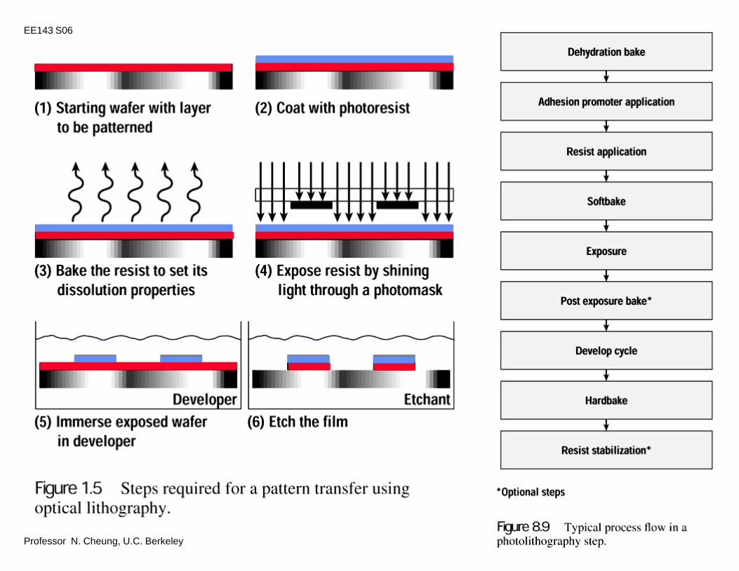
EE143 S06 Lecture 11 Photolithographyee243/sp10/EE143/lectures/Lec_11.pdfEE143 S06 Lecture 11 12...
43
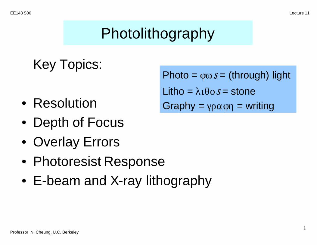
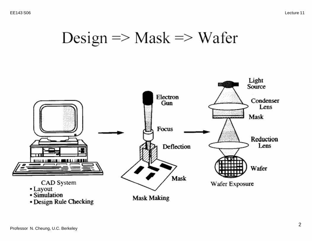
Professor N. Cheung, U.C. Berkeley Lecture 11 EE143 S06 1 Photolithography • Resolution • Depth of Focus • Overlay Errors • Photoresist Response • E-beam and X-ray lithography Key Topics: Photo = φϖ s = (through) light Litho = λιθοs = stone Graphy = γραφη = writing
Transcript of EE143 S06 Lecture 11 Photolithographyee243/sp10/EE143/lectures/Lec_11.pdfEE143 S06 Lecture 11 12...
Professor N. Cheung, U.C. Berkeley
Lecture 11EE143 S06
1
Photolithography
• Resolution• Depth of Focus• Overlay Errors• Photoresist Response• E-beam and X-ray lithography
Key Topics:Photo = φωs = (through) light
Litho = λιθοs = stoneGraphy = γραφη = writing
Professor N. Cheung, U.C. Berkeley
Lecture 11EE143 S06
2
Professor N. Cheung, U.C. Berkeley
Lecture 11EE143 S06
3
Professor N. Cheung, U.C. Berkeley
Lecture 11EE143 S06
4
Professor N. Cheung, U.C. Berkeley
Lecture 11EE143 S06
5
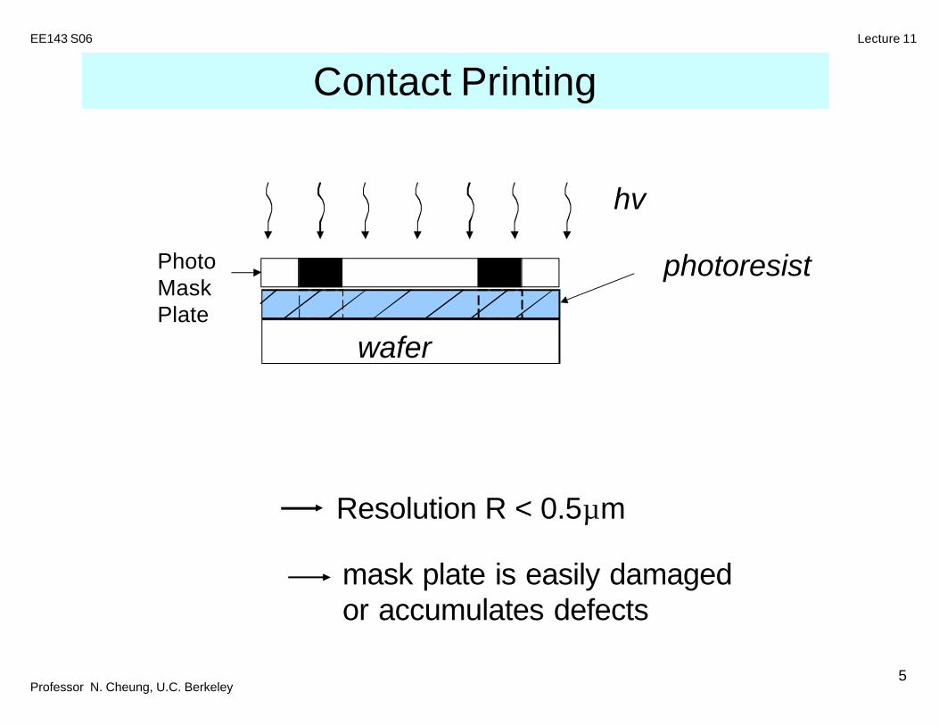
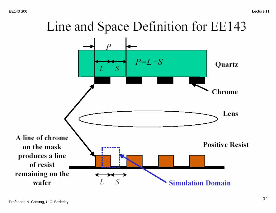
Contact Printing
wafer
hv
photoresist
Resolution R < 0.5µm
mask plate is easily damagedor accumulates defects
PhotoMaskPlate
Professor N. Cheung, U.C. Berkeley
Lecture 11EE143 S06
6
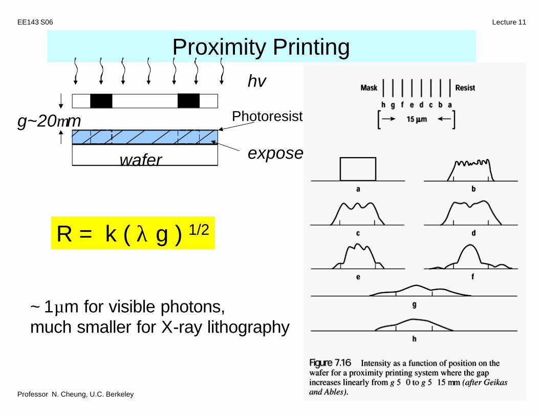
Proximity Printing
wafer
hv
g~20µm
exposed
Photoresist
x
R = k ( λ g ) 1/2
~ 1µm for visible photons,much smaller for X-ray lithography
Professor N. Cheung, U.C. Berkeley
Lecture 11EE143 S06
7
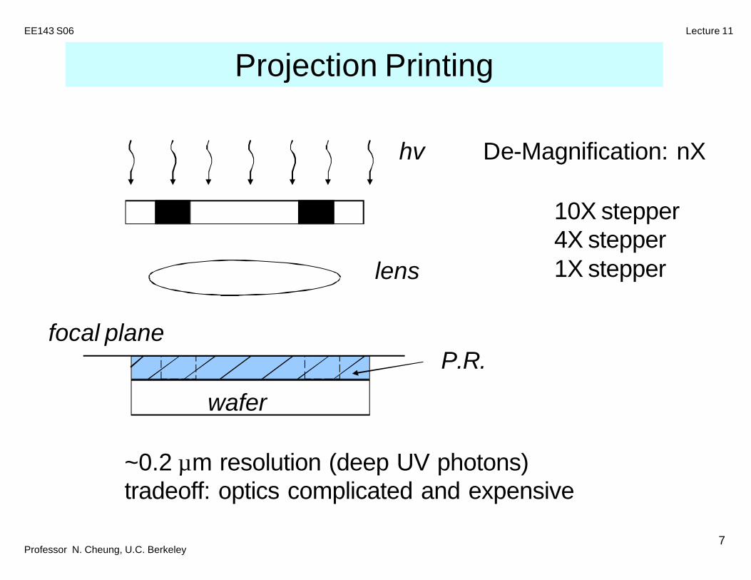
Projection Printing
hv
lens
wafer
P.R.focal plane
~0.2 µm resolution (deep UV photons)tradeoff: optics complicated and expensive
De-Magnification: nX
10X stepper4X stepper1X stepper
Professor N. Cheung, U.C. Berkeley
Lecture 11EE143 S06
8
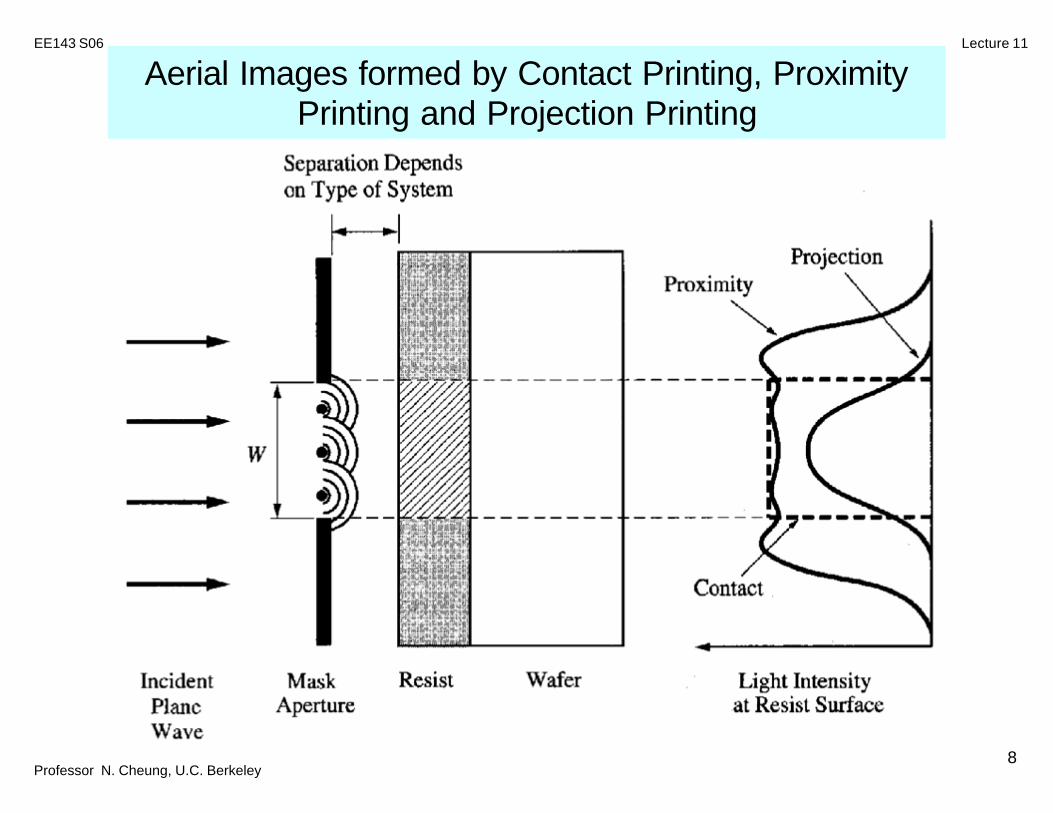
Aerial Images formed by Contact Printing, Proximity Printing and Projection Printing
Professor N. Cheung, U.C. Berkeley
Lecture 11EE143 S06
9
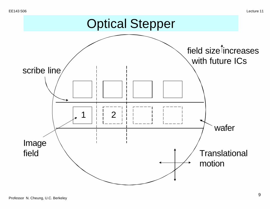
Optical Stepper
wafer
scribe line
1 2
Imagefield
field size increaseswith future ICs
Translationalmotion
Professor N. Cheung, U.C. Berkeley
Lecture 11EE143 S06
10
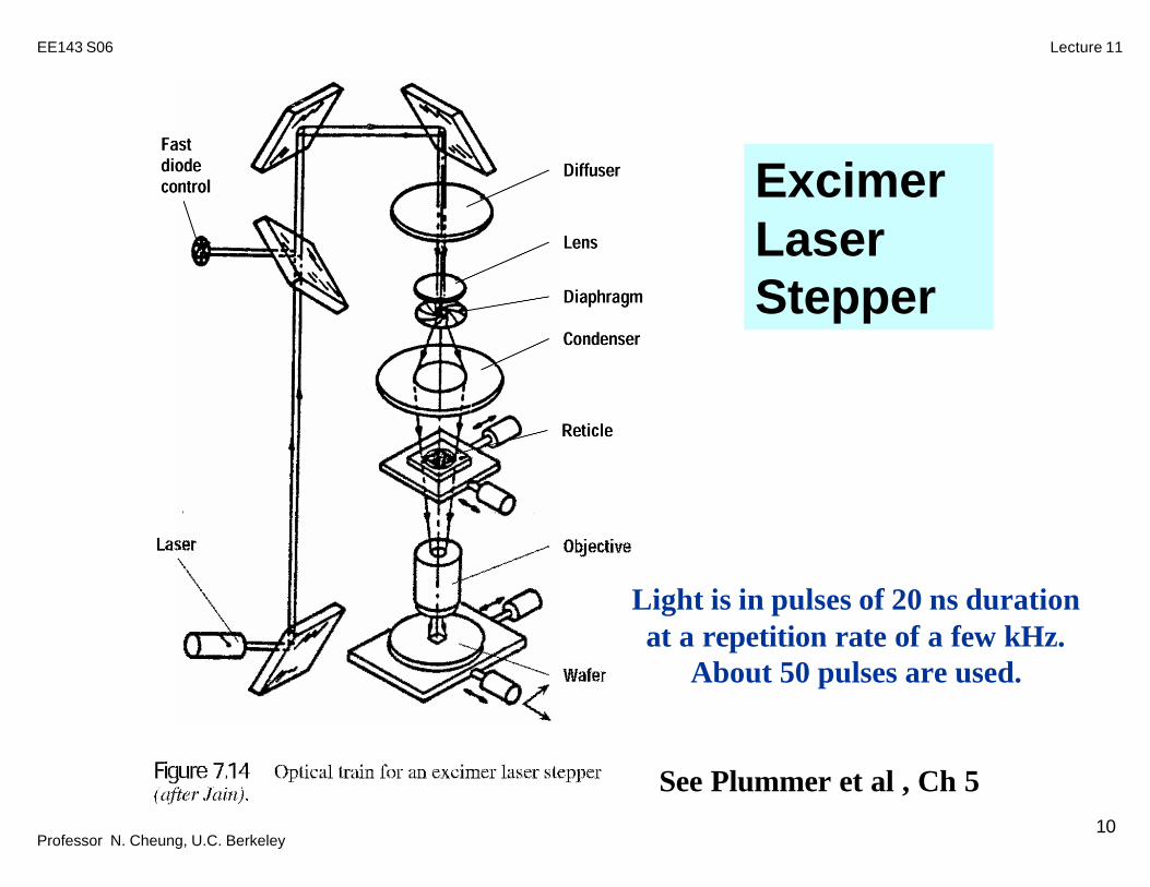
Excimer LaserStepper
Light is in pulses of 20 ns duration at a repetition rate of a few kHz.
About 50 pulses are used.
See Plummer et al , Ch 5
Professor N. Cheung, U.C. Berkeley
Lecture 11EE143 S06
11
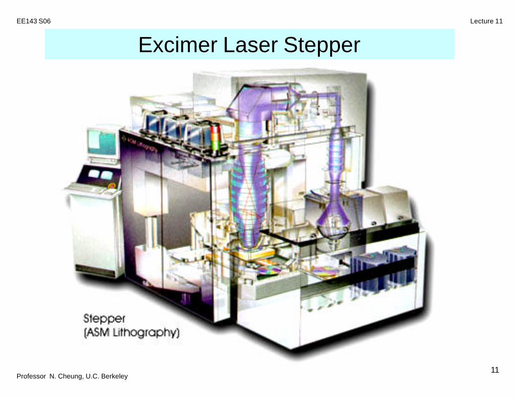
Excimer Laser Stepper
Professor N. Cheung, U.C. Berkeley
Lecture 11EE143 S06
12
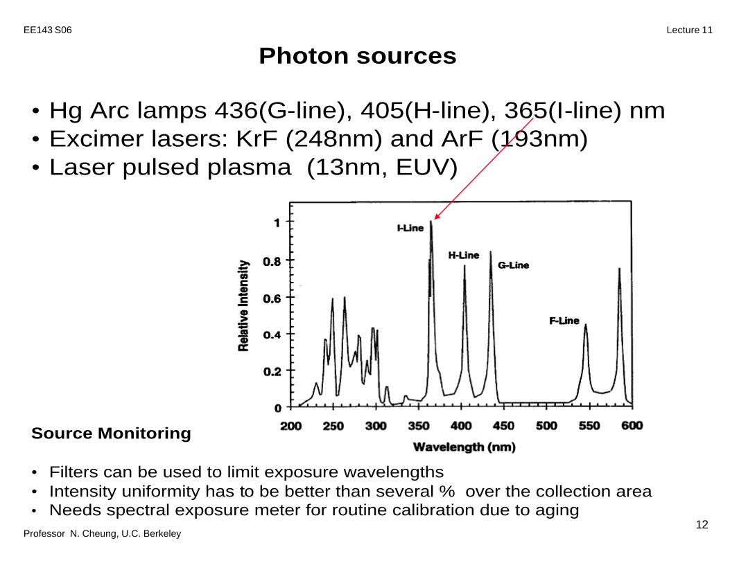
Photon sources • Hg Arc lamps 436(G-line), 405(H-line), 365(I-line) nm • Excimer lasers: KrF (248nm) and ArF (193nm) • Laser pulsed plasma (13nm, EUV) Source Monitoring • Filters can be used to limit exposure wavelengths • Intensity uniformity has to be better than several % over the collection area • Needs spectral exposure meter for routine calibration due to aging
Professor N. Cheung, U.C. Berkeley
Lecture 11EE143 S06
13
Professor N. Cheung, U.C. Berkeley
Lecture 11EE143 S06
14
Professor N. Cheung, U.C. Berkeley
Lecture 11EE143 S06
15
Professor N. Cheung, U.C. Berkeley
Lecture 11EE143 S06
16
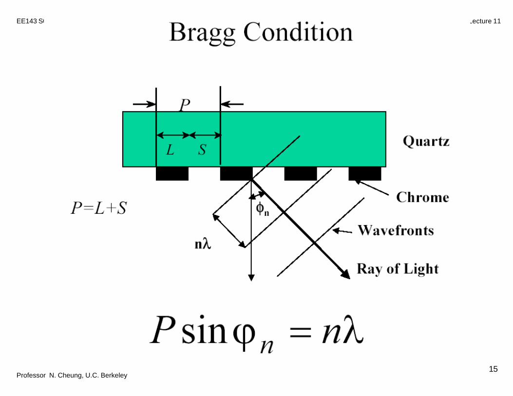
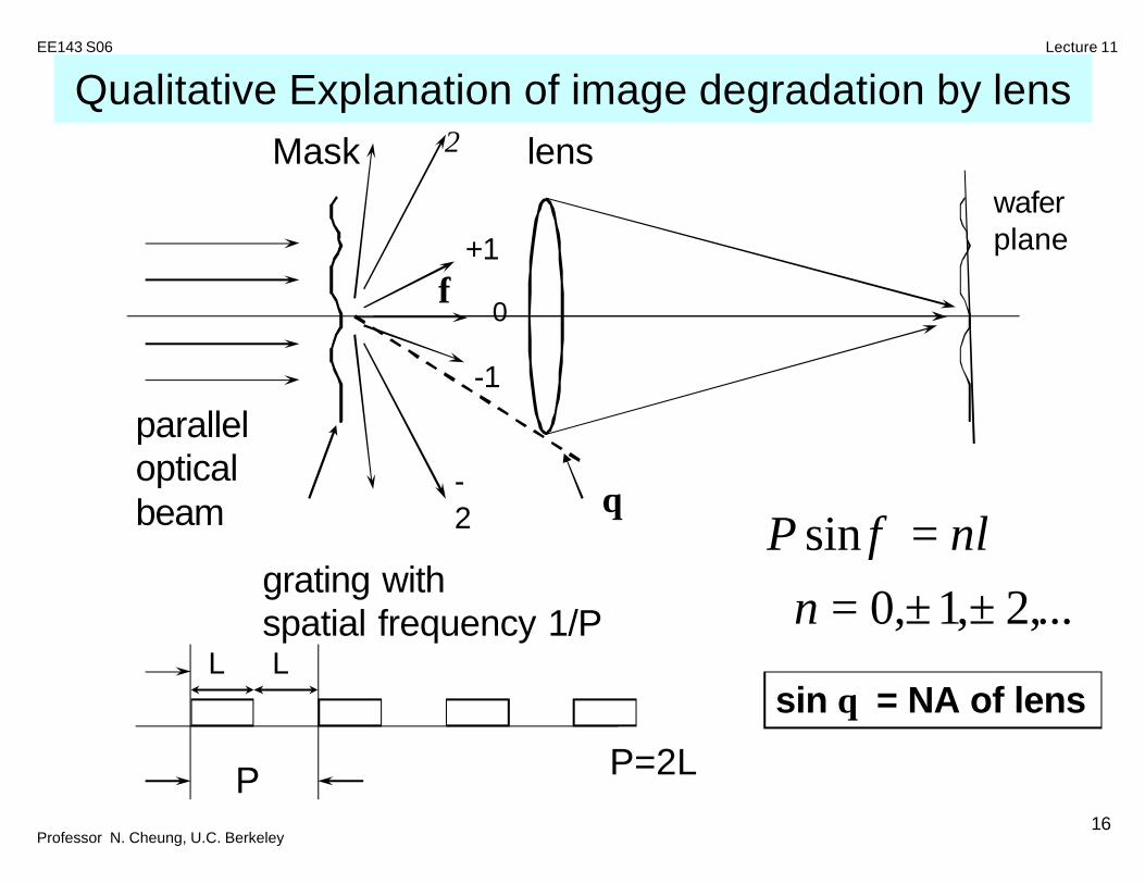
waferplane
parallelopticalbeam
grating withspatial frequency 1/P
P P=2L
...,2,1,0sin
±±==
nnP λφ
-1
-2
+1
+2Mask lens
L L
0
sin θ = NA of lens
φ
θ
Qualitative Explanation of image degradation by lens
Professor N. Cheung, U.C. Berkeley
Lecture 11EE143 S06
17
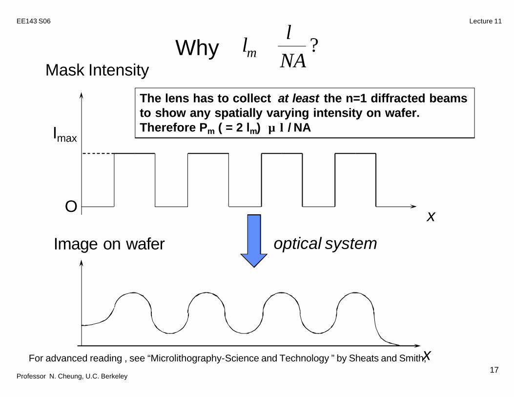
x
Why lNAm ∝λ
?
x
Image on wafer optical system
Mask Intensity
Imax
O
The lens has to collect at least the n=1 diffracted beamsto show any spatially varying intensity on wafer.Therefore Pm ( = 2 lm) ∝ λ / NA
For advanced reading , see “Microlithography-Science and Technology ” by Sheats and Smith,
Professor N. Cheung, U.C. Berkeley
Lecture 11EE143 S06
18
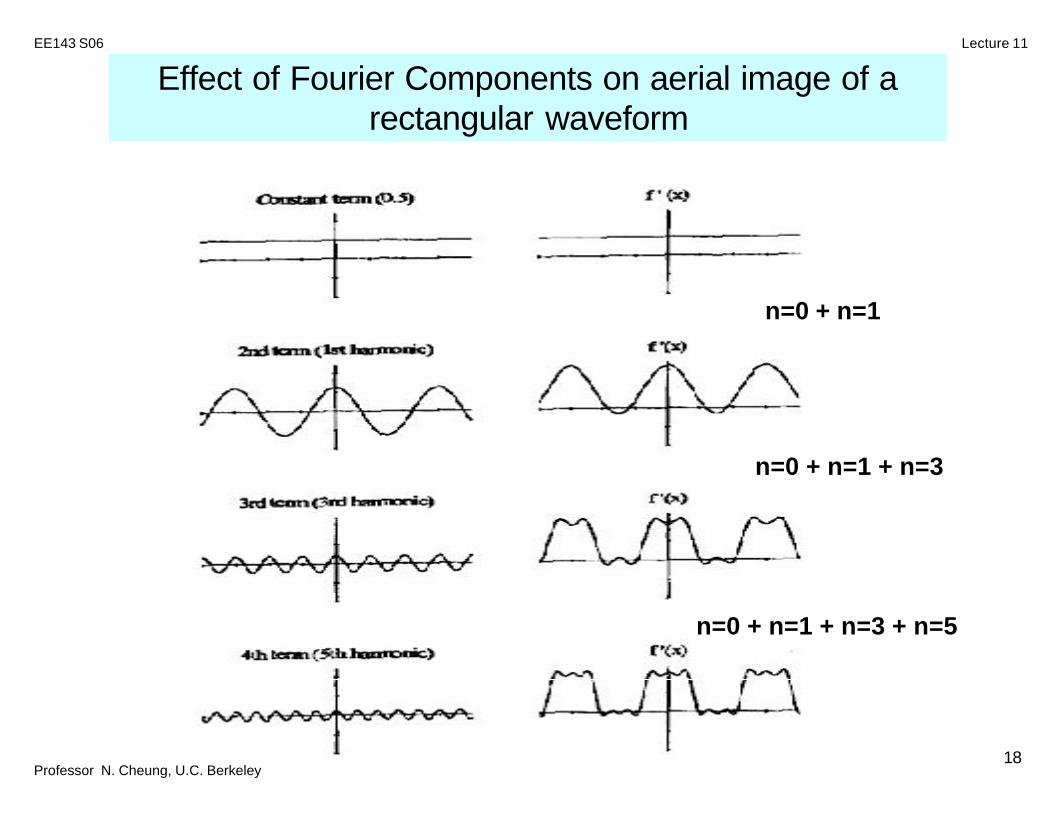
n=0
n=0 + n=1
n=0 + n=1 + n=3
n=0 + n=1 + n=3 + n=5
Effect of Fourier Components on aerial image of a rectangular waveform
Professor N. Cheung, U.C. Berkeley
Lecture 11EE143 S06
19
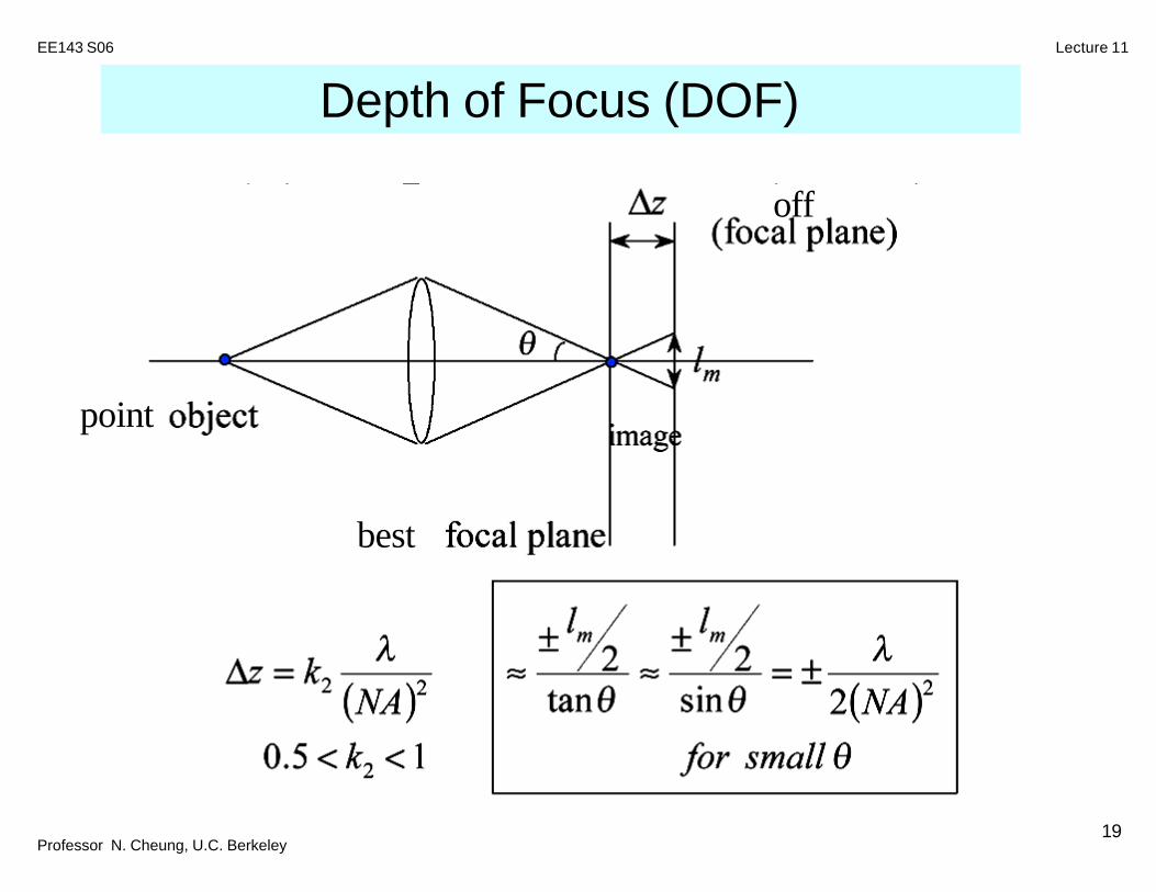
point
best
off
Depth of Focus (DOF)
Professor N. Cheung, U.C. Berkeley
Lecture 11EE143 S06
20
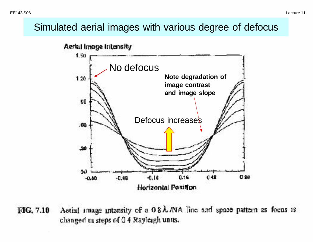
No defocus
Defocus increases
Note degradation of image contrast and image slope
Simulated aerial images with various degree of defocus
Professor N. Cheung, U.C. Berkeley
Lecture 11EE143 S06
21
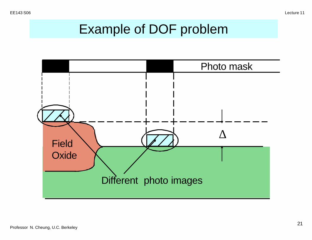
∆FieldOxide
Photo mask
Different photo images
Example of DOF problem
Professor N. Cheung, U.C. Berkeley
Lecture 11EE143 S06
22
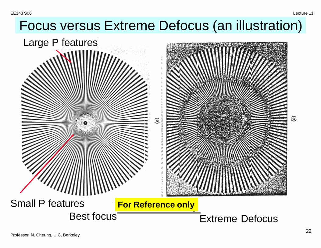
For Reference onlyBest focus Extreme Defocus
Large P features
Small P features
Focus versus Extreme Defocus (an illustration)
Professor N. Cheung, U.C. Berkeley
Lecture 11EE143 S06
23
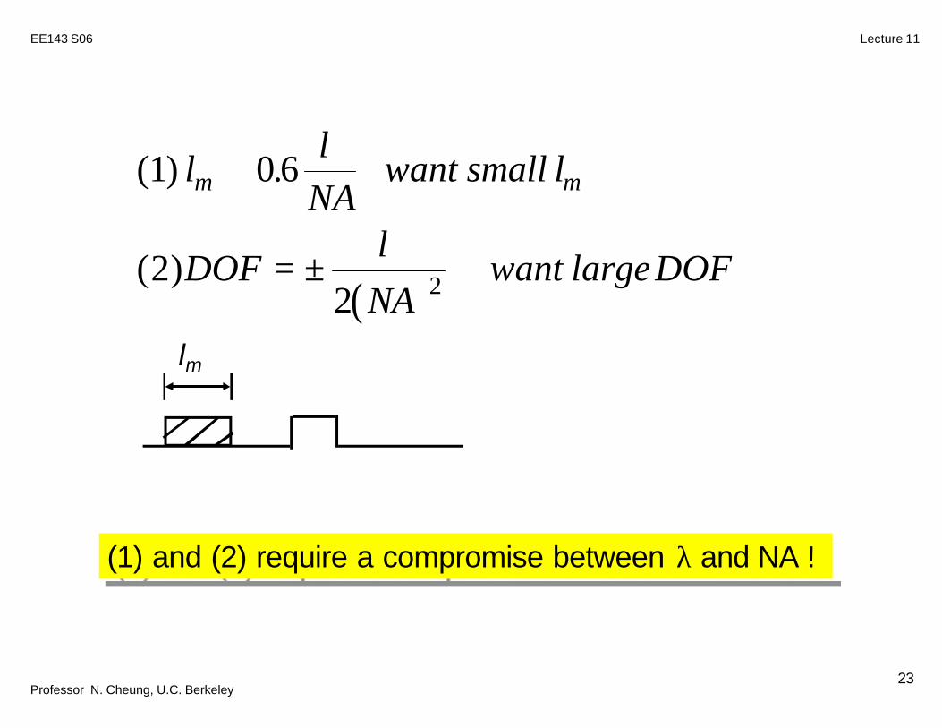
( )
( ) .
( )
1 0 6
22 2
lNA
want small l
DOFNA
want largeDOF
m m≅
= ±
λ
λ
lm
(1) and (2) require a compromise between λ and NA !
Professor N. Cheung, U.C. Berkeley
Lecture 11EE143 S06
24
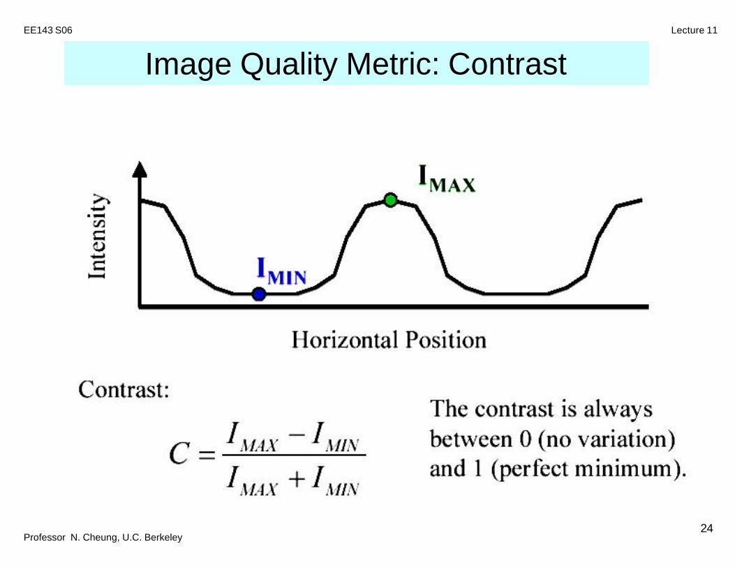
Image Quality Metric: Contrast
Professor N. Cheung, U.C. Berkeley
Lecture 11EE143 S06
25
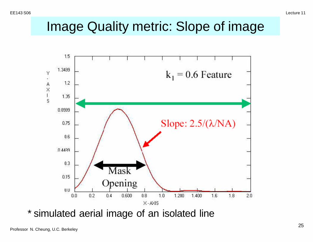
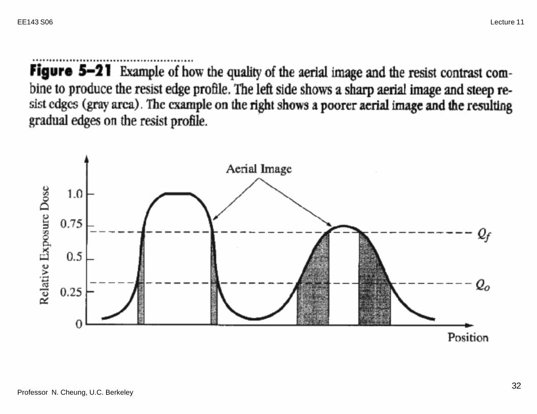
* simulated aerial image of an isolated line
Image Quality metric: Slope of image
Professor N. Cheung, U.C. Berkeley
Lecture 11EE143 S06
26
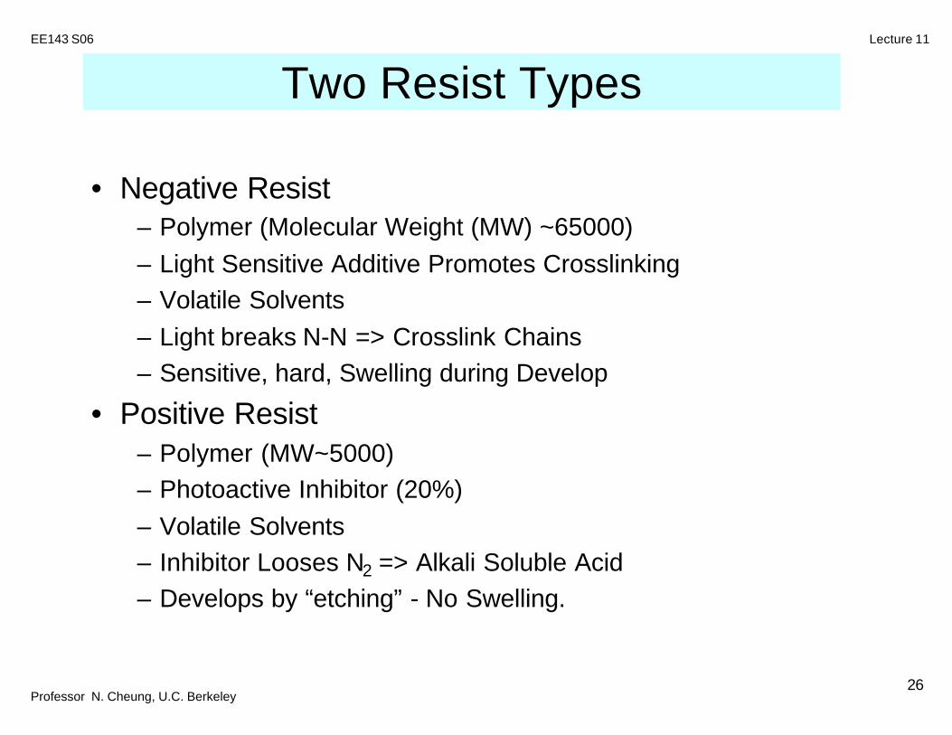
Two Resist Types
• Negative Resist – Polymer (Molecular Weight (MW) ~65000)– Light Sensitive Additive Promotes Crosslinking– Volatile Solvents– Light breaks N-N => Crosslink Chains– Sensitive, hard, Swelling during Develop
• Positive Resist– Polymer (MW~5000)– Photoactive Inhibitor (20%)– Volatile Solvents– Inhibitor Looses N2 => Alkali Soluble Acid– Develops by “etching” - No Swelling.
Professor N. Cheung, U.C. Berkeley
Lecture 11EE143 S06
27
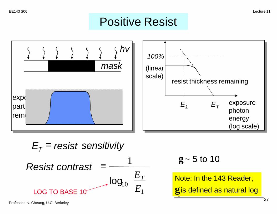
hv
mask
P.R.exposed part is removed
=E resist sensitivity
Resist contrastΕΕ
T
Τ
≡
1
101
log
100%
E1 ETexposurephotonenergy(log scale)
resist thickness remaining
(linearscale)
γ ~ 5 to 10
LOG TO BASE 10
Note: In the 143 Reader,
γ is defined as natural log
Positive Resist
Professor N. Cheung, U.C. Berkeley
Lecture 11EE143 S06
28
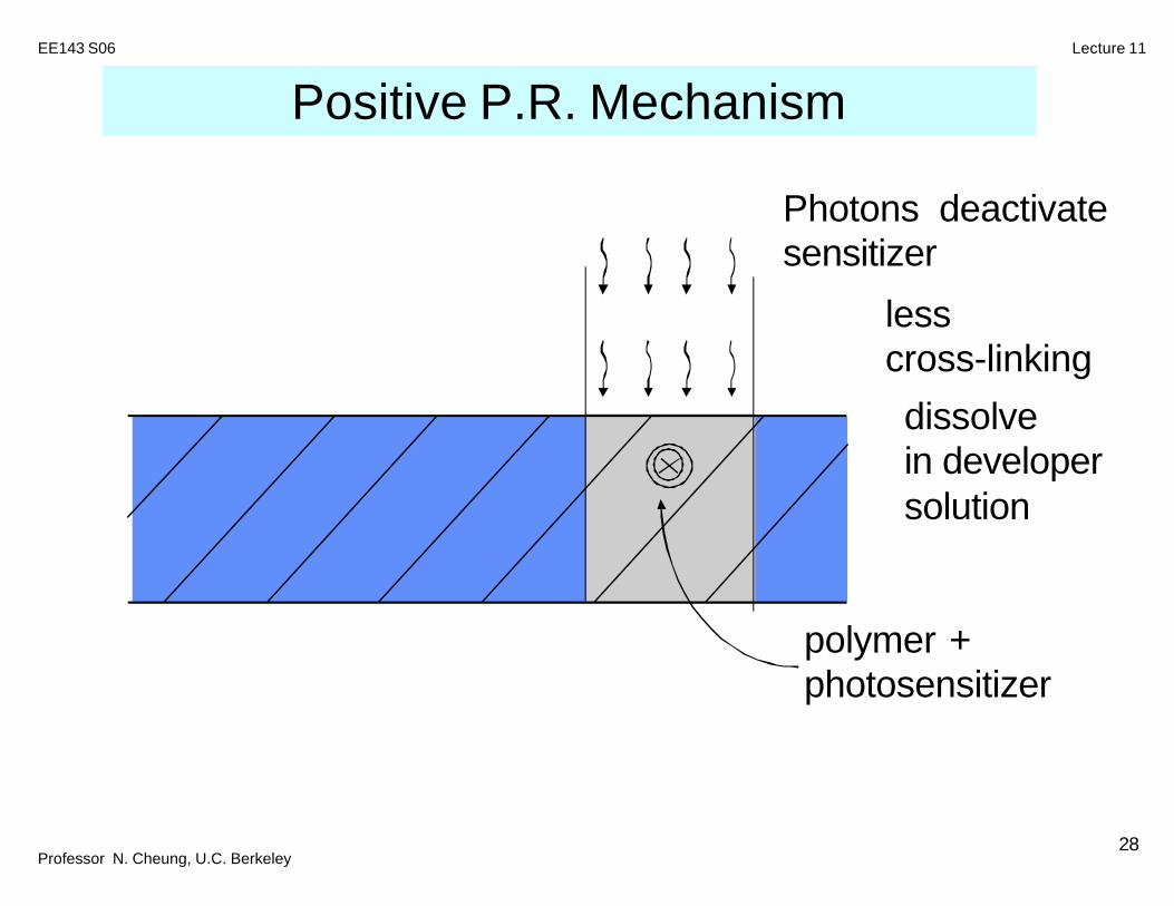
Positive P.R. Mechanism
Photons deactivatesensitizer
polymer +photosensitizer
less cross-linking
⇒
dissolvein developersolution
⇒
Professor N. Cheung, U.C. Berkeley
Lecture 11EE143 S06
29
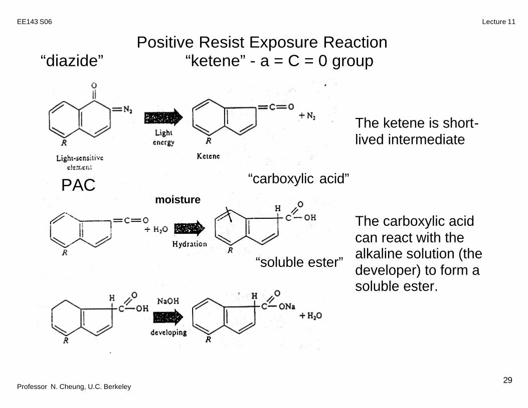
Positive Resist Exposure Reaction “diazide” “ketene” - a = C = 0 group
moisture
“carboxylic acid”
“soluble ester”
The ketene is short-lived intermediate The carboxylic acid can react with the alkaline solution (the developer) to form a soluble ester.
PAC
Professor N. Cheung, U.C. Berkeley
Lecture 11EE143 S06
30
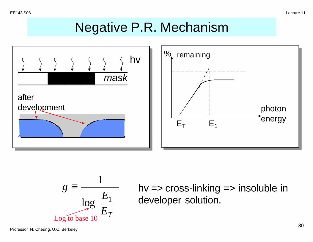
Negative P.R. Mechanism
hv
E1ET
remaining
photonenergy
after development
γ ≡
1
1logEET
%
Log to base 10
mask
hv => cross-linking => insoluble in developer solution.
Professor N. Cheung, U.C. Berkeley
Lecture 11EE143 S06
31
resistresist
substrate
resist
substrate
resist
Position x
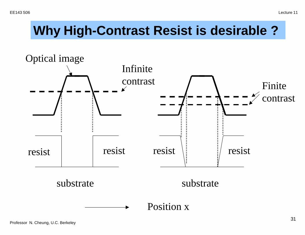
Finitecontrast
Infinitecontrast
Optical image
Why High-Contrast Resist is desirable ?
Professor N. Cheung, U.C. Berkeley
Lecture 11EE143 S06
32
Professor N. Cheung, U.C. Berkeley
Lecture 11EE143 S06
33
Positive vs. Negative Photoresists
• Positive P.R.:ü higher resolutionü aqueous-based solventsû less sensitive
• Negative P.R.:ümore sensitive => higher exposure throughputü relatively tolerant of developing conditionsü better chemical resistance => better mask materialü less expensiveû lower resolutionû organic-based solvents
Professor N. Cheung, U.C. Berkeley
Lecture 11EE143 S06
34
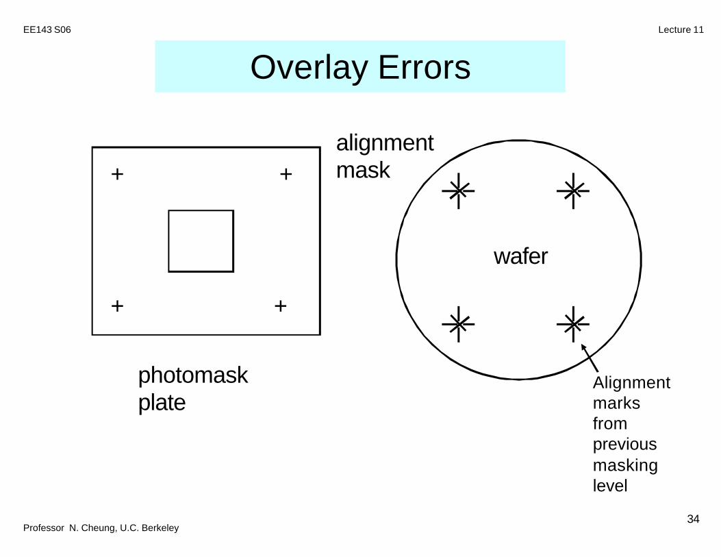
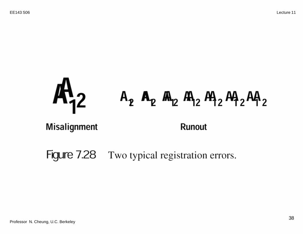
Overlay Errors
+
+
+
+
Alignmentmarksfrom previousmaskinglevel
wafer
alignmentmask
photomaskplate
Professor N. Cheung, U.C. Berkeley
Lecture 11EE143 S06
35
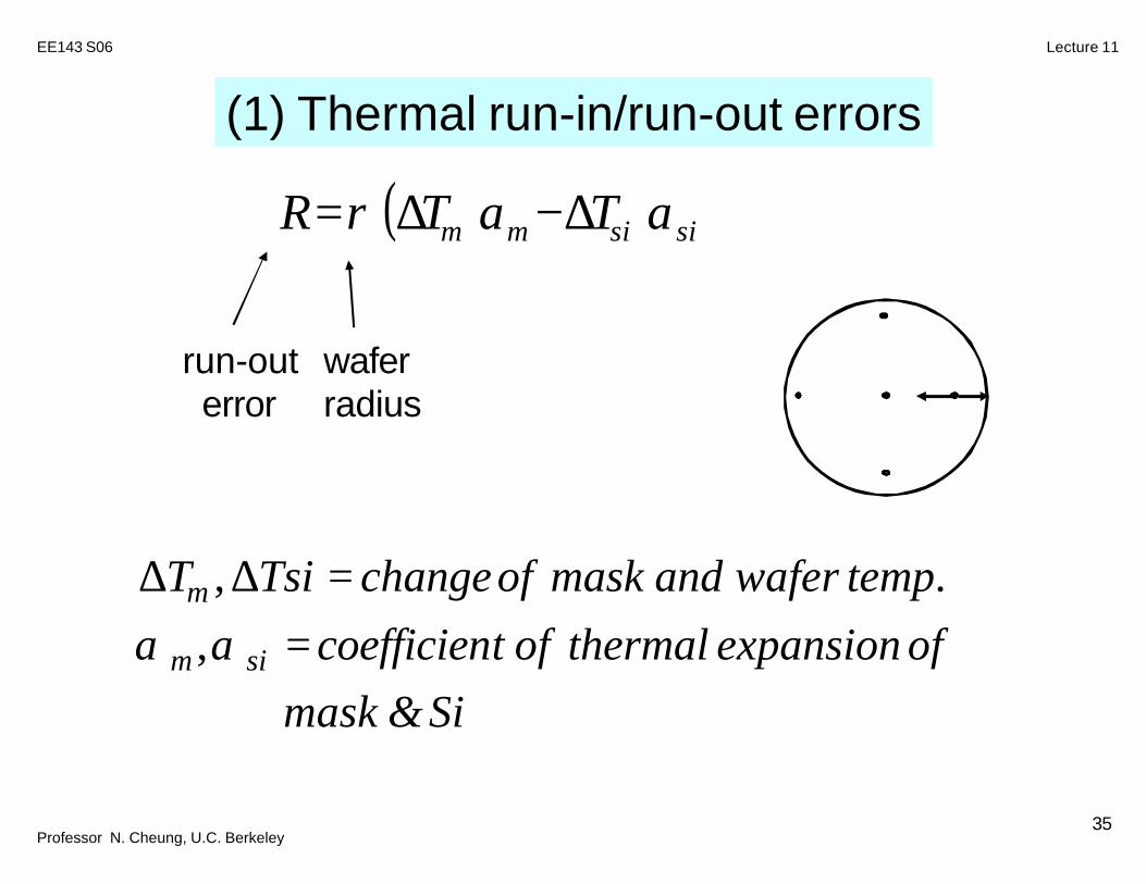
(1) Thermal run-in/run-out errors
( )sisimm TTrR αα ⋅∆−⋅∆⋅=
∆ ∆T Tsi changeof mask and wafer tempcoefficient of thermal expansion of
mask & Si
m
m si
, .,
==α α
run-outerror
waferradius
Professor N. Cheung, U.C. Berkeley
Lecture 11EE143 S06
36
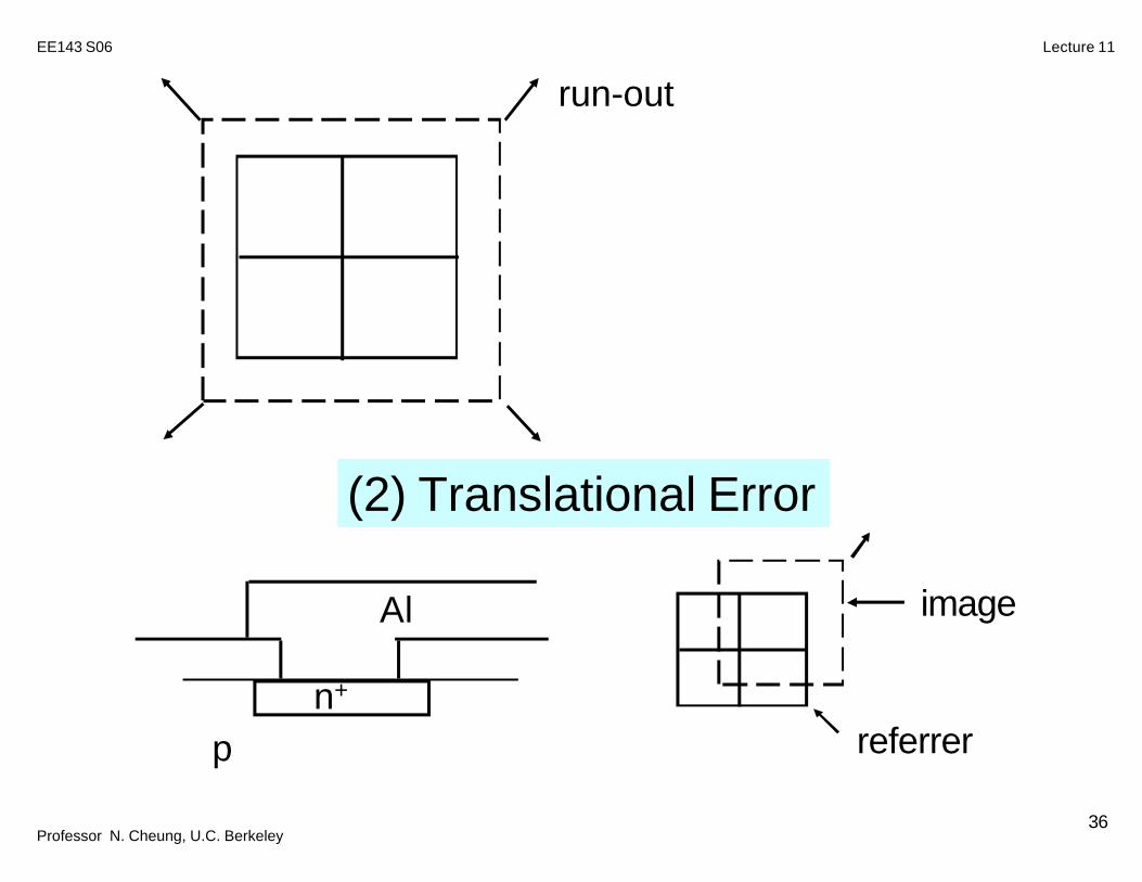
run-out
(2) Translational Error
referrer
image
n+
Al
p
Professor N. Cheung, U.C. Berkeley
Lecture 11EE143 S06
37
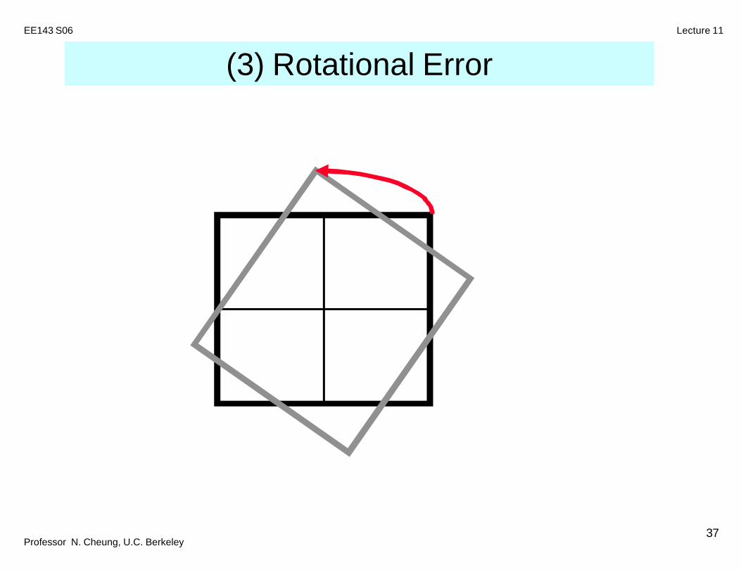
(3) Rotational Error
Professor N. Cheung, U.C. Berkeley
Lecture 11EE143 S06
38
Professor N. Cheung, U.C. Berkeley
Lecture 11EE143 S06
39
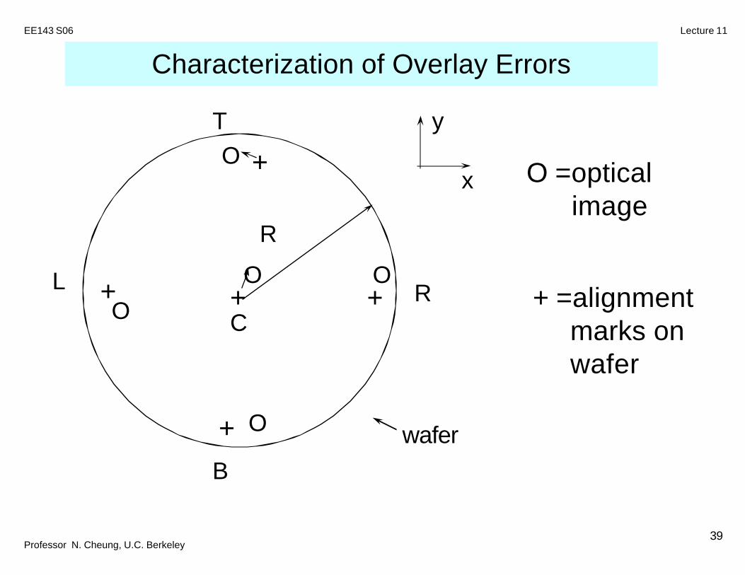
Characterization of Overlay Errors
+ +
+
+
L
T
B
R
wafer
O
O
O
O
+
R
O
O =opticalimage
+ =alignmentmarks onwafer
y
x
C
Professor N. Cheung, U.C. Berkeley
Lecture 11EE143 S06
40
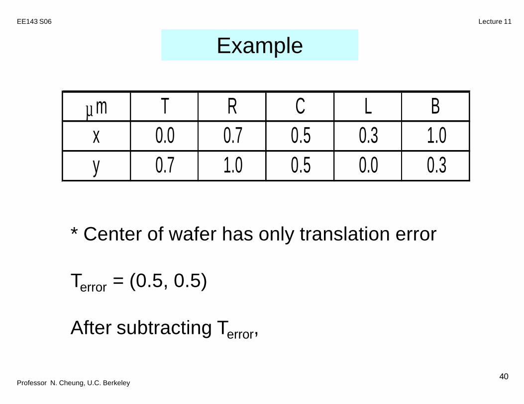
µ m T R C L Bx 0.0 0.7 0.5 0.3 1.0y 0.7 1.0 0.5 0.0 0.3
* Center of wafer has only translation error
Terror = (0.5, 0.5)
After subtracting Terror,
Example
Professor N. Cheung, U.C. Berkeley
Lecture 11EE143 S06
41
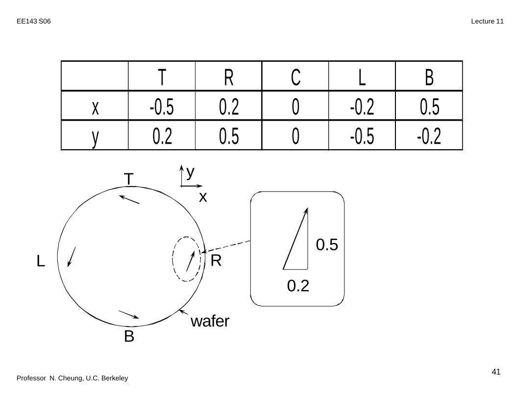
T R C L Bx -0.5 0.2 0 -0.2 0.5y 0.2 0.5 0 -0.5 -0.2
T
B
R
wafer
yx
L0.5
0.2
Professor N. Cheung, U.C. Berkeley
Lecture 11EE143 S06
42
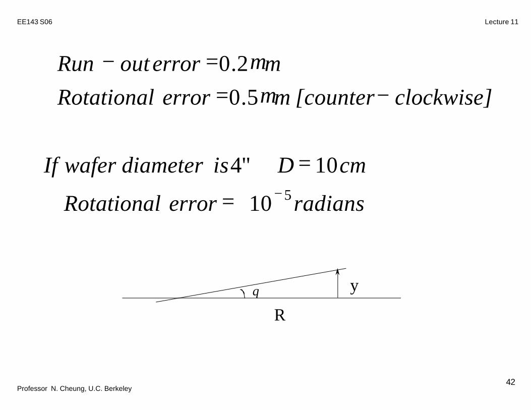
radianserrorRotational
cmDisdiameterwaferIf
clockwise][countermerrorRotationalmerroroutRun
510
10"4
5.02.0
−=∴
=⇒
−=∴=−∴
µµ
θ
R
y
Professor N. Cheung, U.C. Berkeley
Lecture 11EE143 S06
43
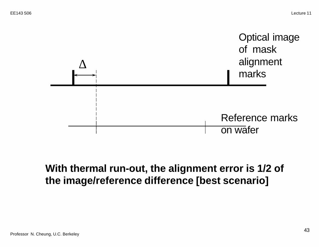
Reference markson wafer
Optical imageof mask alignmentmarks
∆
With thermal run-out, the alignment error is 1/2 of the image/reference difference [best scenario]