ECS642U Embedded Systems Digital I/O William Marsh.
33
ECS642U Embedded Systems Digital I/O William Marsh
-
Upload
sophie-brenda-spencer -
Category
Documents
-
view
242 -
download
2
Transcript of ECS642U Embedded Systems Digital I/O William Marsh.
ECS642U Embedded Systems
Digital I/O
William Marsh

2ARM University ProgramCopyright © ARM Ltd 2013
Acknowledgement
•Some slides from ARM University Program lab-in-a-box•Copyright acknowledged
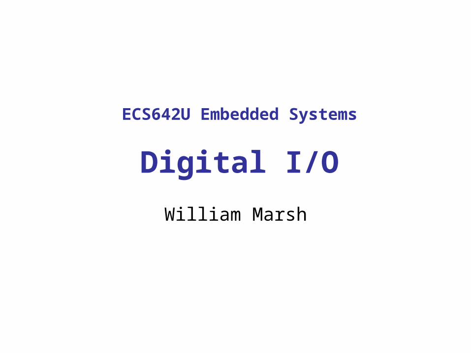
Outline
• Principles of memory mapped I/O• Using Keil μVision
– Compile, Assemble, Link, Load– Memory map– Debug
• KL25Z memory layout• GPIO Configuration and use
– Bus Matrix– Pin multiplexing– Data direction– GPIO ports

Using KeilμVision
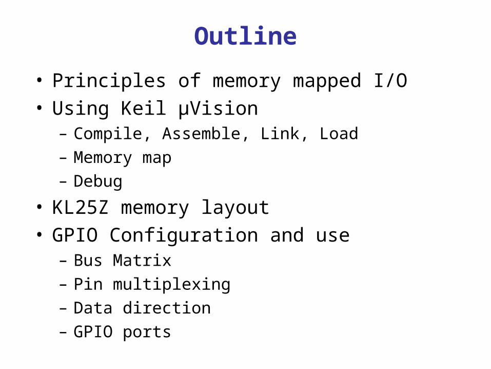
Compiling a Program
• Compile C program assembly code
• Link with libraries memory image
• Download
• Debug– Set breakpoints– Monitor variables
PCFreedom KL25Z
SDA debug
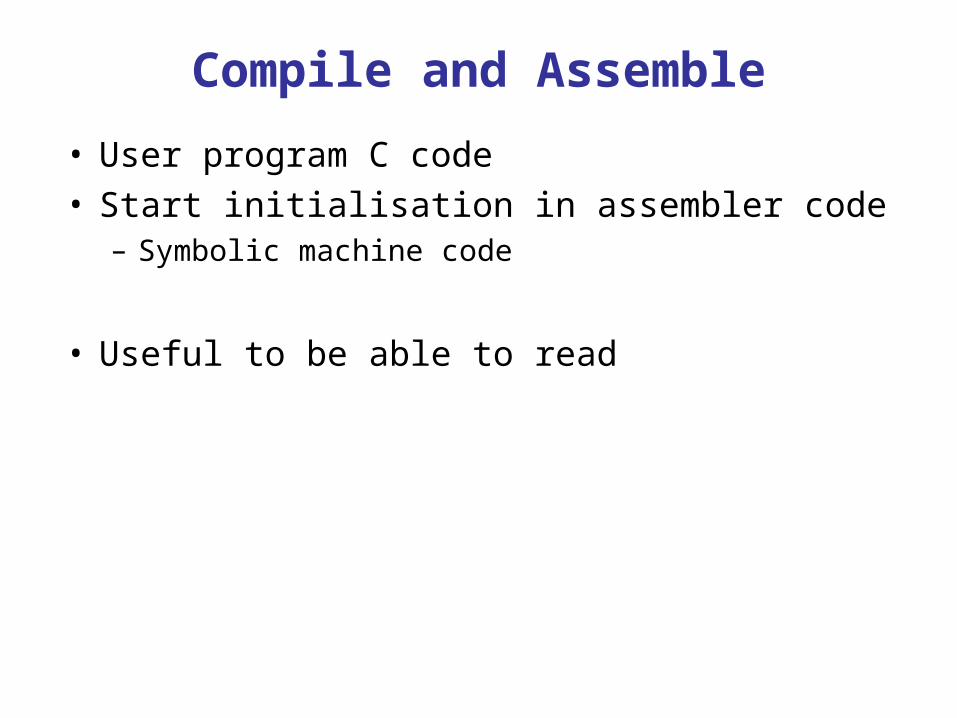
Compile and Assemble
• User program C code• Start initialisation in assembler code
– Symbolic machine code
• Useful to be able to read
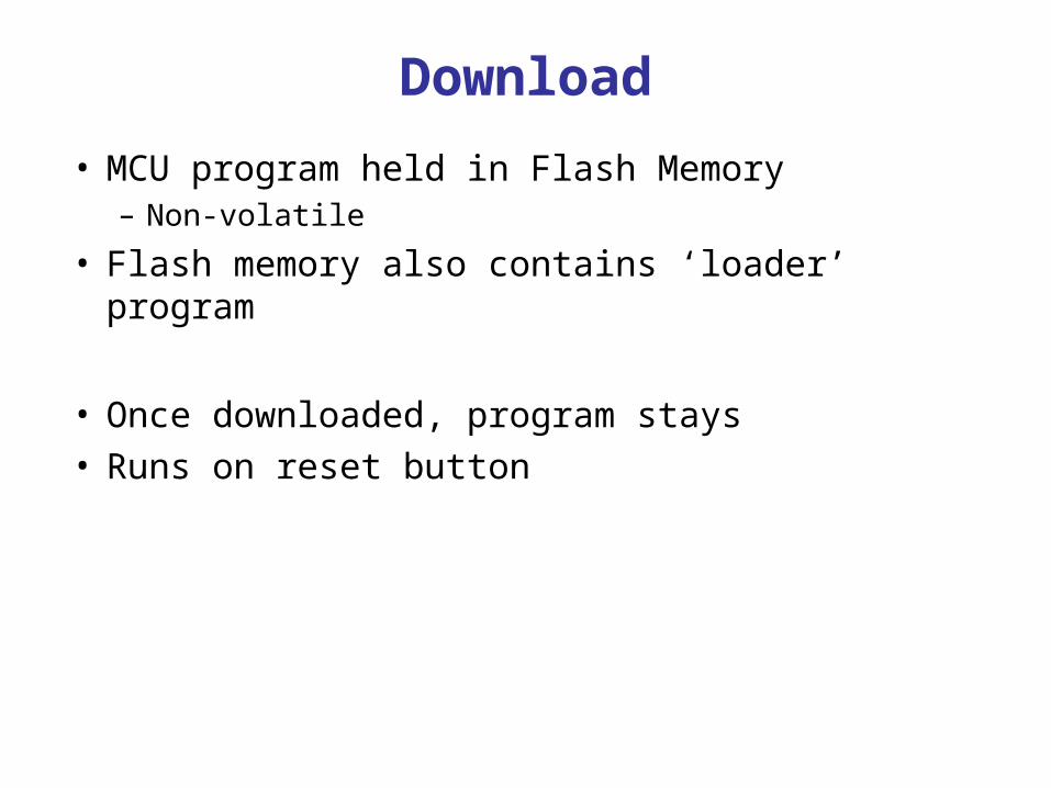
Download
• MCU program held in Flash Memory– Non-volatile
• Flash memory also contains ‘loader’ program
• Once downloaded, program stays• Runs on reset button
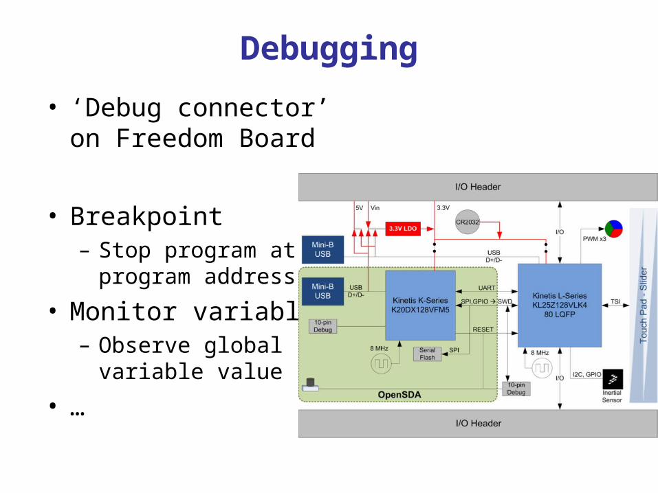
Debugging
• ‘Debug connector’ on Freedom Board
• Breakpoint– Stop program at a
program address
• Monitor variable– Observe global
variable value
• …
Memory Mapped I/O
Memory Mapped I/O
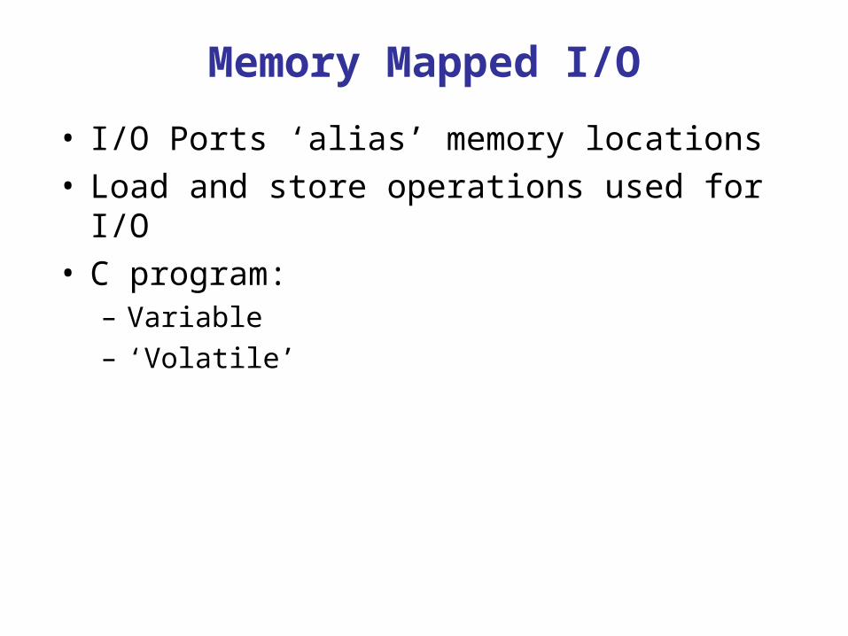
• I/O Ports ‘alias’ memory locations• Load and store operations used for I/O• C program:
– Variable– ‘Volatile’
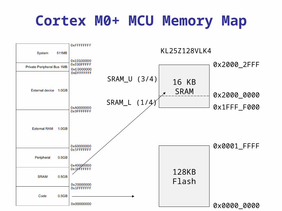
Cortex M0+ MCU Memory Map
0x0000_0000
0x0001_FFFF
16 KB SRAM
128KB Flash
0x2000_0000
0x2000_2FFF
0x1FFF_F000
SRAM_U (3/4)
SRAM_L (1/4)
KL25Z128VLK4
Memory Areas
• Flash memory– 0x0000 0000 – 0x0001 FFFF– 128 KByte– Used for program code
• SRAM– Data (or code)– 16 KBytes: 0x1FFF F000 - 0x2000 2FFF
General Purpose I/O
Overview
• How do we make a program light up LEDs• GPIO – General Purpose I/O
– Basic Concepts– Port Circuitry– Control Registers– Accessing Hardware Registers in C– Clocking and Muxing
• Circuit Interfacing– Inputs– Outputs
• Additional Port Configuration

Basic Concepts
• GPIO– Input: is input signal is a 1 or a 0?– Output: set output to 1 or 0
• Can use this to interface with external devices– Input: switch– Output: LEDs
3 Colour LED on the KL25Z
board is active low

Output Example: Driving LEDs
• Safe current for– LED and– MCU port driver
• Use resistor– R = (VDD – VLED)/ILED
• Set ILED = 4 mA• VLED depends on LED colour
– Red: ~1.8V Blue: ~2.7 V
• Solve for R given VDD = ~3.0 V– Red: 300Ω Blue: 75Ω
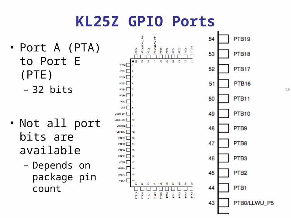
KL25Z GPIO Ports
• Port A (PTA) to Port E (PTE)– 32 bits
• Not all port bits are available– Depends on
package pin count
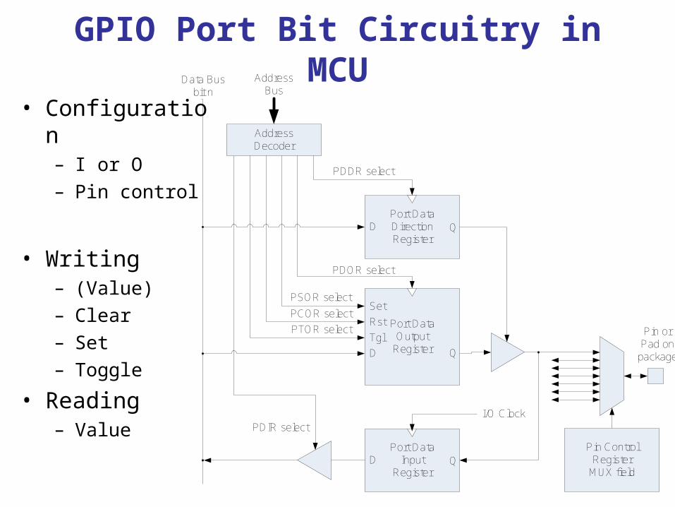
GPIO Port Bit Circuitry in MCU
• Configuration– I or O– Pin control
• Writing– (Value)– Clear– Set– Toggle
• Reading– Value
PDOR select
PDIR select
PDDR select
Data Bus bit n
Port Data Direction Register
D Q
Port Data Output
RegisterD Q
AddressDecoder
Address Bus
Pin or Pad on
package
Port Data Input
RegisterD Q
I/O Clock
Tgl
Rst
SetPSOR select
PCOR select
PTOR select
Pin Control Register
MUX field
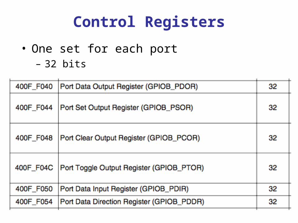
Control Registers
• One set for each port– 32 bits
PDOR select
PDIR select
PDDR select
Data Bus bit n
Port Data Direction Register
D Q
Port Data Output
RegisterD Q
AddressDecoder
Address Bus
Pin or Pad on
package
Port Data Input
RegisterD Q
I/O Clock
Tgl
Rst
SetPSOR select
PCOR select
PTOR select
Pin Control Register
MUX field
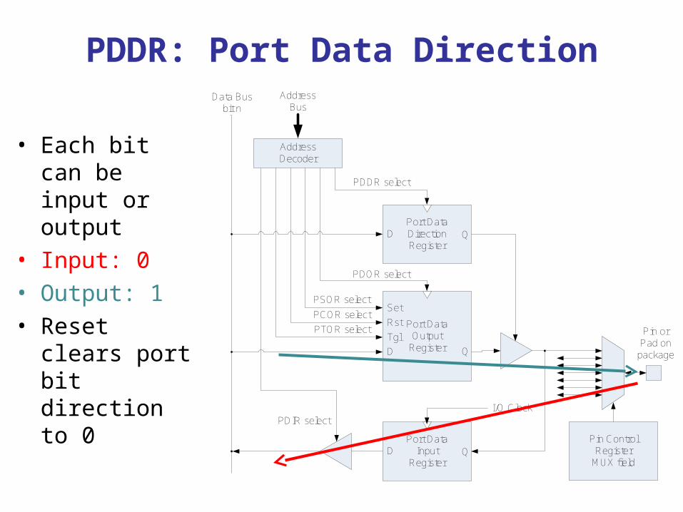
PDDR: Port Data Direction
• Each bit can be input or output
• Input: 0• Output: 1• Reset clears
port bit direction to 0
PDOR select
PDIR select
PDDR select
Data Bus bit n
Port Data Direction Register
D Q
Port Data Output
RegisterD Q
AddressDecoder
Address Bus
Pin or Pad on
package
Port Data Input
RegisterD Q
I/O Clock
Tgl
Rst
SetPSOR select
PCOR select
PTOR select
Pin Control Register
MUX field
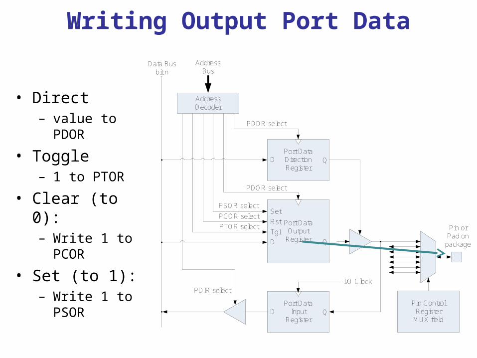
Writing Output Port Data
• Direct– value to
PDOR
• Toggle– 1 to PTOR
• Clear (to 0): – Write 1 to
PCOR
• Set (to 1): – Write 1 to
PSOR
PDOR select
PDIR select
PDDR select
Data Bus bit n
Port Data Direction Register
D Q
Port Data Output
RegisterD Q
AddressDecoder
Address Bus
Pin or Pad on
package
Port Data Input
RegisterD Q
I/O Clock
Tgl
Rst
SetPSOR select
PCOR select
PTOR select
Pin Control Register
MUX field
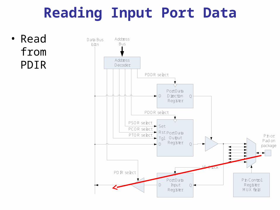
Reading Input Port Data
• Read from PDIR
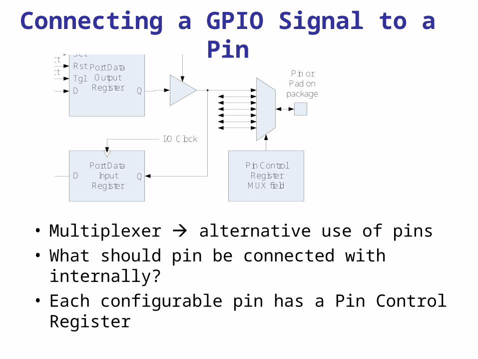
Connecting a GPIO Signal to a Pin
• Multiplexer alternative use of pins • What should pin be connected with
internally?• Each configurable pin has a Pin Control
Register
PDOR select
PDIR select
PDDR select
Data Bus bit n
Port Data Direction Register
D Q
Port Data Output
RegisterD Q
AddressDecoder
Address Bus
Pin or Pad on
package
Port Data Input
RegisterD Q
I/O Clock
Tgl
Rst
SetPSOR select
PCOR select
PTOR select
Freescale: is the pin mux location in this diagram accurate?
Pin Control Register
MUX field

Alternative Pin Configuration
• Each pin has multiple uses
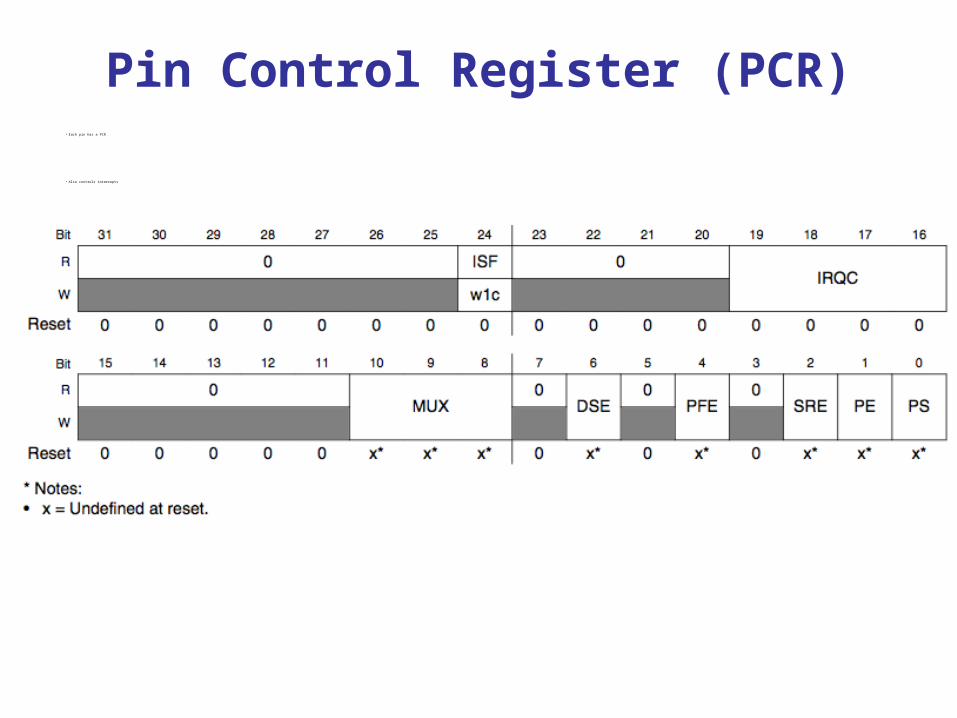
Pin Control Register (PCR)• Each pin has a PCR
• Also controls interrupts
Pin Control Register (PCR)
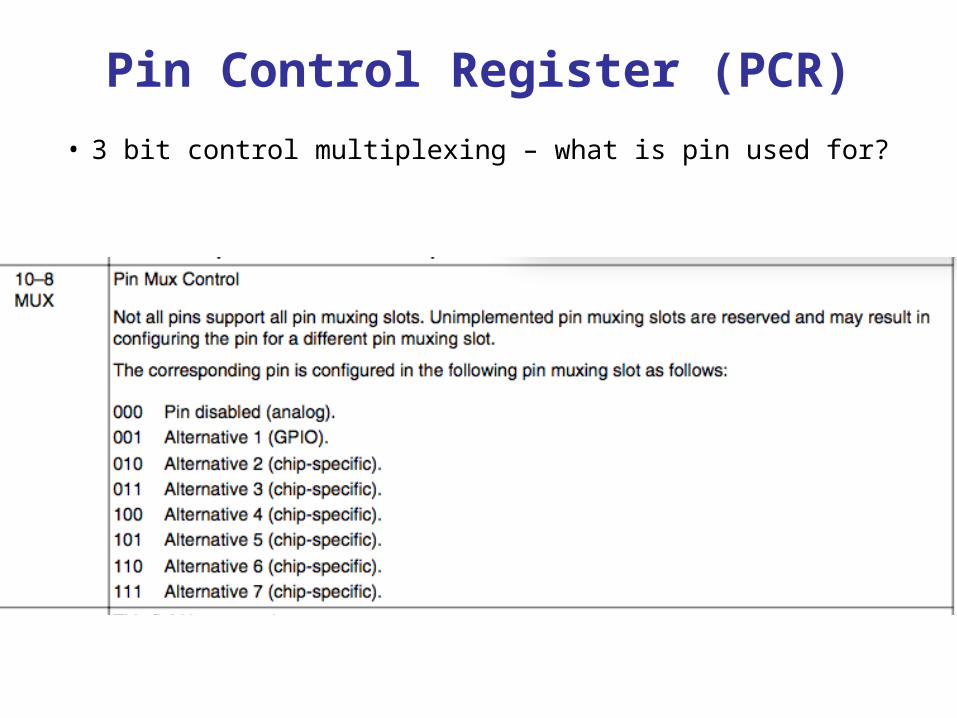
• 3 bit control multiplexing – what is pin used for?
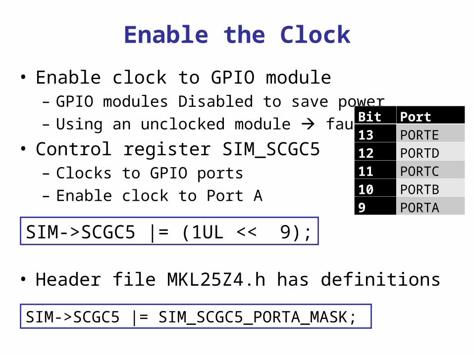
Enable the Clock
• Enable clock to GPIO module– GPIO modules Disabled to save power– Using an unclocked module fault
• Control register SIM_SCGC5 – Clocks to GPIO ports– Enable clock to Port A
• Header file MKL25Z4.h has definitions
Bit Port13 PORTE12 PORTD11 PORTC10 PORTB9 PORTA
SIM->SCGC5 |= (1UL << 9);
SIM->SCGC5 |= SIM_SCGC5_PORTA_MASK;
Summary of Configuration
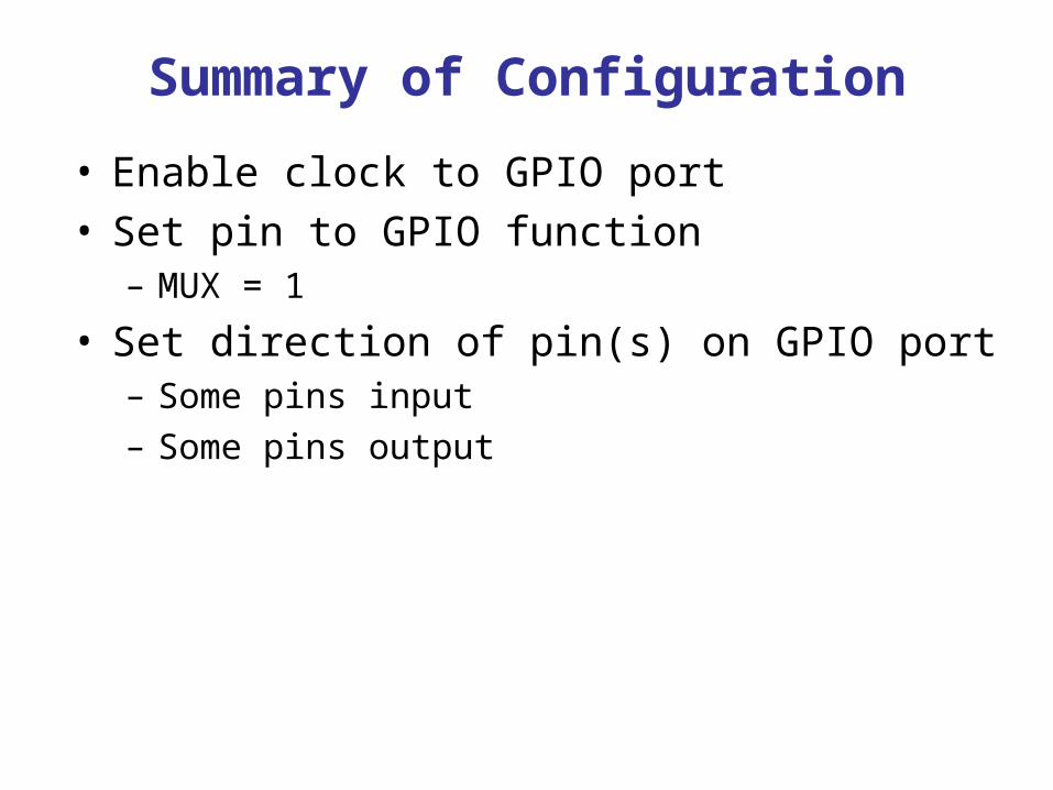
• Enable clock to GPIO port• Set pin to GPIO function
– MUX = 1
• Set direction of pin(s) on GPIO port– Some pins input– Some pins output
Review of Configuration Code

Config Code – Review
• Enable clock
• Note– bitwise or of two masks– |= used to leave other bits unchanged
// Enable clock to ports B and D
SIM->SCGC5 |=
SIM_SCGC5_PORTB_MASK | SIM_SCGC5_PORTD_MASK;
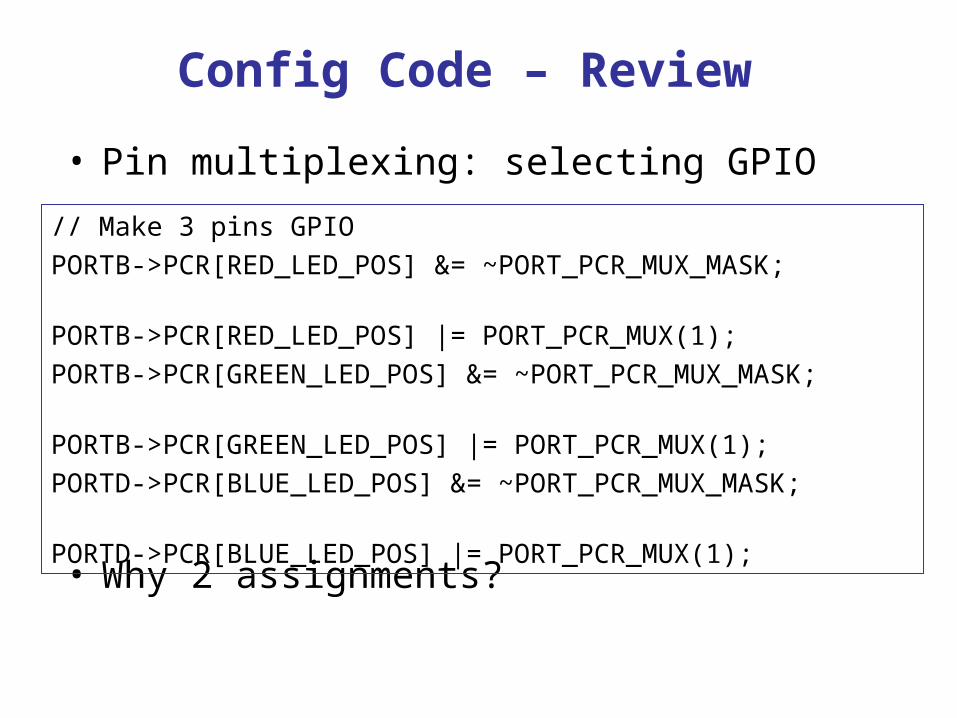
Config Code – Review
• Pin multiplexing: selecting GPIO
• Why 2 assignments?
// Make 3 pins GPIO
PORTB->PCR[RED_LED_POS] &= ~PORT_PCR_MUX_MASK;
PORTB->PCR[RED_LED_POS] |= PORT_PCR_MUX(1);
PORTB->PCR[GREEN_LED_POS] &= ~PORT_PCR_MUX_MASK;
PORTB->PCR[GREEN_LED_POS] |= PORT_PCR_MUX(1);
PORTD->PCR[BLUE_LED_POS] &= ~PORT_PCR_MUX_MASK;
PORTD->PCR[BLUE_LED_POS] |= PORT_PCR_MUX(1);

Config Code – Review • Make ports output:
– data direction register
// Set ports to outputs
PTB->PDDR |= MASK(RED_LED_POS) | MASK(GREEN_LED_POS);
PTD->PDDR |= MASK(BLUE_LED_POS);

Summary
• Memory mapped I/O has registers for:– For configuring operation– For doing I/O
• Most pins are multiplexed– All pins are GPIO
• Also have to configure clocks signal to GPIO Port