Dynamic Logic - Duke University
7
Krish Chakrabarty 1 Dynamic Logic M p M e V DD PDN In 1 In 2 In 3 Out M e M p V DD PUN In 1 In 2 In 3 Out C L C L 2 phase operation: • Evaluation • Precharge Φ Φ Φ n network Φp network Φ Φ Krish Chakrabarty 2 Dynamic Logic • N+2 transistors for N-input function – Better than 2N transistors for complementary static CMOS – Comparable to N+1 for ratio-ed logic • No static power dissipation – Better than ratio-ed logic • Careful design, clock signal Φ needed
Transcript of Dynamic Logic - Duke University
1
Krish Chakrabarty 1
Dynamic Logic
Mp
Me
VDD
PDNIn1In2In3
OutMe
Mp
VDD
PUNIn1In2In3
Out
CL
CL
2 phase operation:• Evaluation
• PrechargeΦ
Φ
Φ
n network Φp network
Φ
Φ
Krish Chakrabarty 2
Dynamic Logic• N+2 transistors for N-input function
– Better than 2N transistors for complementary static CMOS – Comparable to N+1 for ratio-ed logic
• No static power dissipation– Better than ratio-ed logic
• Careful design, clock signal Φ needed

2
Krish Chakrabarty 3
Example
Mp
Me
VDD
Out
A
B
C
• Ratio les s
• No Static Power Cons umption
• Nois e Margins s mall (NML)
• Requires Clock
Φ
Φ
Krish Chakrabarty 4
Dynamic Logic: Principles
Mp
Me
VDD
PDNIn1In2In3
Out
CL
Φ
Φ
• PrechargeΦ = 0, Out is precharged to VDD by Mp.Me is turned off, no dc current flows(regardless of input values)
• EvaluationΦ = 1, Me is turned on, Mp is turned off.Output is pulled down to zero dependingon the values on the inputs. If not, precharged value remains on CL.
Important: Once Out is discharged, it cannot be charged again!Gate input can make only one transition during evaluation
• Minimum clock frequency must be maintained• Can Me be eliminated?

3
Krish Chakrabarty 5
Dynamic 4 Input NAND Gate
In1In2In3In4
Out
VDD
GNDφ
Krish Chakrabarty 6
Reliability Problems — Charge Leakage
Mp
Me
VDD
Out
ACL(1)
(2)
t
t
Vout
(b) Effect on waveforms(a) Leakage sources
precharge evaluate
Minimum Clock Frequency: > 1 MHz
A = 0
Φ
ΦΦ
(1) Leakage through reverse-biased diode of the diffusion area(2) Subthreshold current from drain to source

4
Krish Chakrabarty 7
Charge Sharing (redistribution)
Mp
Me
VDD
Out
A
B = 0
CL
Ca
Cb
Ma
Mb
X
• Assume: during precharge, A and B are 0, Ca is discharged• During evaluation, B remains 0 and A rises to 1• Charge stored on CL is now redistributed over CL and Ca
CLVDD = CL Vout(t) + CaVX
VX = VDD - Vt, thereforeδVout(t) = Vout(t) - VDD = (VDD-Vt)CL
Ca
Desirable to keep the voltage drop below thresholdof pMOS transistor (why?) ⇒ Ca/CL < 0.2
Krish Chakrabarty 8
Charge Redistribution - Solutions
Mp
Me
VDD
OutA
B
Ma
Mb
Mbl Mp
Me
VDD
Out
A
B
Ma
Mb
Mbl
(b) Precharge of internal nodes(a) Static bleeder
Φ
Φ Φ
Φ
Φ
5
Krish Chakrabarty 9
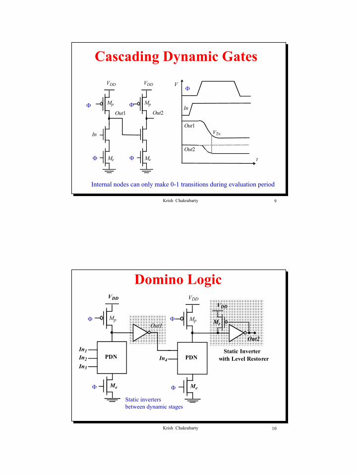
Cascading Dynamic Gates
Mp
Me
VDD
Mp
Me
VDD
In
Out1 Out2Φ
Φ
Φ
Φ
Internal nodes can only make 0-1 transitions during evaluation period
Out2
Out1
In
V
t
VTn
Φ
Krish Chakrabarty 10
Domino Logic
Mp
Me
VDD
PDNIn1In2In3
Out1Mp
Me
VDD
PDNIn4
Out2
Mr
VDD
Static Inverterwith Level Restorer
Φ
Φ
Φ
Φ
Static invertersbetween dynamic stages

6
Krish Chakrabarty 11
Domino Logic - Characteristics
• Only non-inverting logic
• Very fast - Only 1->0 transitions at input of inverter
• Adding level restorer reduces leakage andcharge redistribution problems
• Optimize inverter for fan-out
• Precharging makes pull-up very fast
Krish Chakrabarty 12
np-CMOS (Zipper CMOS)
Mp
Me
VDD
PDNIn1In2In3
Me
Mp
VDD
PUNIn4
Out1
Out2
Φ
Φ
Φ
Φ
• Only 1-0 transitions allowed at inputs of PUN• Used a lot in the Alpha design

7
Krish Chakrabarty 13
np CMOS Adder
VDDφ
φCi0
A0 B0 B0
φ
A0
VDDφ
B1
φ
A1
VDDφ
φ
A1 B1
Ci1
Ci2
Ci0Ci0
B0
A0B0
S0
A0
VDDφ
φ
VDDφ
VDDφ
φ
B1 Ci1B1
φ
A1A1
VDDφ S1
Ci1
Carry Path
Krish Chakrabarty 14
CMOS Circuit Styles - Summary