Dual MicroPower LinCMOS Voltage Comparators (Rev. E) · PDF filedual micropower lincmos™...
38
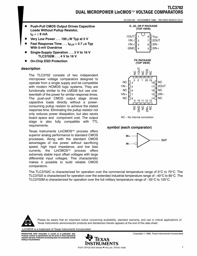
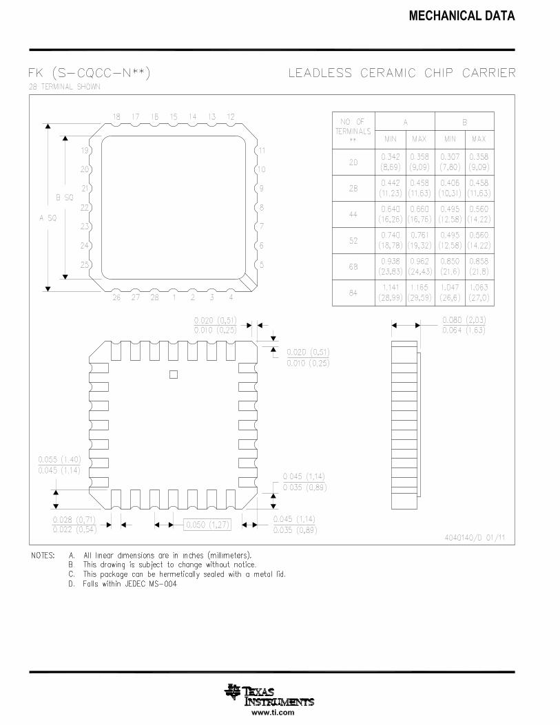
TLC3702 DUAL MICROPOWER LinCMOS™ VOLTAGE COMPARATORS SLCS013E − NOVEMBER 1986 − REVISED MARCH 2012 1 POST OFFICE BOX 655303 • DALLAS, TEXAS 75265 D Push-Pull CMOS Output Drives Capacitive Loads Without Pullup Resistor, I O = ± 8 mA D Very Low Power . . . 100 μW Typ at 5 V D Fast Response Time . . . t PLH = 2.7 μs Typ With 5-mV Overdrive D Single-Supply Operation . . . 3 V to 16 V TLC3702M . . . 4 V to 16 V D On-Chip ESD Protection description The TLC3702 consists of two independent micropower voltage comparators designed to operate from a single supply and be compatible with modern HCMOS logic systems. They are functionally similar to the LM339 but use one- twentieth of the power for similar response times. The push-pull CMOS output stage drives capacitive loads directly without a power- consuming pullup resistor to achieve the stated response time. Eliminating the pullup resistor not only reduces power dissipation, but also saves board space and component cost. The output stage is also fully compatible with TTL requirements. Texas Instruments LinCMOS™ process offers superior analog performance to standard CMOS processes. Along with the standard CMOS advantages of low power without sacrificing speed, high input impedance, and low bias currents, the LinCMOS™ process offers extremely stable input offset voltages with large differential input voltages. This characteristic makes it possible to build reliable CMOS comparators. The TLC3702C is characterized for operation over the commercial temperature range of 0°C to 70°C. The TLC3702I is characterized for operation over the extended industrial temperature range of −40°C to 85°C. The TLC3702M is characterized for operation over the full military temperature range of −55°C to 125°C. Please be aware that an important notice concerning availability, standard warranty, and use in critical applications of Texas Instruments semiconductor products and disclaimers thereto appears at the end of this data sheet. Copyright © 1998, Texas Instruments Incorporated PRODUCTION DATA information is current as of publication date. Products conform to specifications per the terms of Texas Instruments standard warranty. Production processing does not necessarily include testing of all parameters. 3 2 1 20 19 9 10 11 12 13 4 5 6 7 8 18 17 16 15 14 NC 2OUT NC 2IN − NC NC 1IN − NC 1IN+ NC FK PACKAGE (TOP VIEW) NC 1OUT NC 2IN+ NC V NC GND NC NC DD D, JG, OR P PACKAGE (TOP VIEW) 1 2 3 4 8 7 6 5 1OUT 1IN − 1IN+ GND V DD 2OUT 2IN − 2IN+ NC − No internal connection OUT symbol (each comparator) IN+ IN − LinCMOS is a trademark of Texas Instruments Incorporated.
-
Upload
duongtuyen -
Category
Documents
-
view
241 -
download
6
Transcript of Dual MicroPower LinCMOS Voltage Comparators (Rev. E) · PDF filedual micropower lincmos™...
TLC3702DUAL MICROPOWER LinCMOS™ VOLTAGE COMPARATORS
SLCS013E − NOVEMBER 1986 − REVISED MARCH 2012
1POST OFFICE BOX 655303 • DALLAS, TEXAS 75265
� Push-Pull CMOS Output Drives CapacitiveLoads Without Pullup Resistor,IO = ± 8 mA
� Very Low Power . . . 100 μW Typ at 5 V
� Fast Response Time . . . tPLH = 2.7 μs TypWith 5-mV Overdrive
� Single-Supply Operation . . . 3 V to 16 VTLC3702M . . . 4 V to 16 V
� On-Chip ESD Protection
description
The TLC3702 consists of two independentmicropower voltage comparators designed tooperate from a single supply and be compatiblewith modern HCMOS logic systems. They arefunctionally similar to the LM339 but use one-twentieth of the power for similar response times.The push-pull CMOS output stage drivescapacitive loads directly without a power-consuming pullup resistor to achieve the statedresponse time. Eliminating the pullup resistor notonly reduces power dissipation, but also savesboard space and component cost. The outputstage is also fully compatible with TTLrequirements.
Texas Instruments LinCMOS™ process offerssuperior analog performance to standard CMOSprocesses. Along with the standard CMOSadvantages of low power without sacrificingspeed, high input impedance, and low biascurrents, the LinCMOS™ process offersextremely stable input offset voltages with largedifferential input voltages. This characteristicmakes it possible to build reliable CMOScomparators.
The TLC3702C is characterized for operation over the commercial temperature range of 0°C to 70°C. TheTLC3702I is characterized for operation over the extended industrial temperature range of −40°C to 85°C. TheTLC3702M is characterized for operation over the full military temperature range of −55°C to 125°C.
Please be aware that an important notice concerning availability, standard warranty, and use in critical applications ofTexas Instruments semiconductor products and disclaimers thereto appears at the end of this data sheet.
Copyright © 1998, Texas Instruments IncorporatedPRODUCTION DATA information is current as of publication date.Products conform to specifications per the terms of Texas Instrumentsstandard warranty. Production processing does not necessarily includetesting of all parameters.
3 2 1 20 19
9 10 11 12 13
4
5
6
7
8
18
17
16
15
14
NC2OUTNC2IN−NC
NC1IN−
NC1IN+
NC
FK PACKAGE(TOP VIEW)
NC
1OU
TN
C
2IN
+N
CV N
C
GN
DN
C
NC
DD
D, JG, OR P PACKAGE(TOP VIEW)
1
2
3
4
8
7
6
5
1OUT1IN−1IN+GND
VDD2OUT2IN−2IN+
NC − No internal connection
OUT
symbol (each comparator)
IN+
IN−
LinCMOS is a trademark of Texas Instruments Incorporated.
TLC3702DUAL MICROPOWER LinCMOS™ VOLTAGE COMPARATORS
SLCS013E − NOVEMBER 1986 − REVISED MARCH 2012
2 POST OFFICE BOX 655303 • DALLAS, TEXAS 75265
AVAILABLE OPTIONS
V maxPACKAGES
TAVIOmaxat 25°C SMALL OUTLINE
(D)CERAMIC
(FK)CERAMIC DIP
(JG)PLASTIC DIP
(P)
0°C to 70°C 5 mV TLC3702CD — — TLC3702CP
−40°C to 85°C 5 mV TLC3702ID — — TLC3702IP
−55°C to 125°C 5 mV TLC3702MD TLC3702MFK TLC3702MJG —
The D package is available taped and reeled. Add R suffix to the device type (e.g., TLC3702CDR).
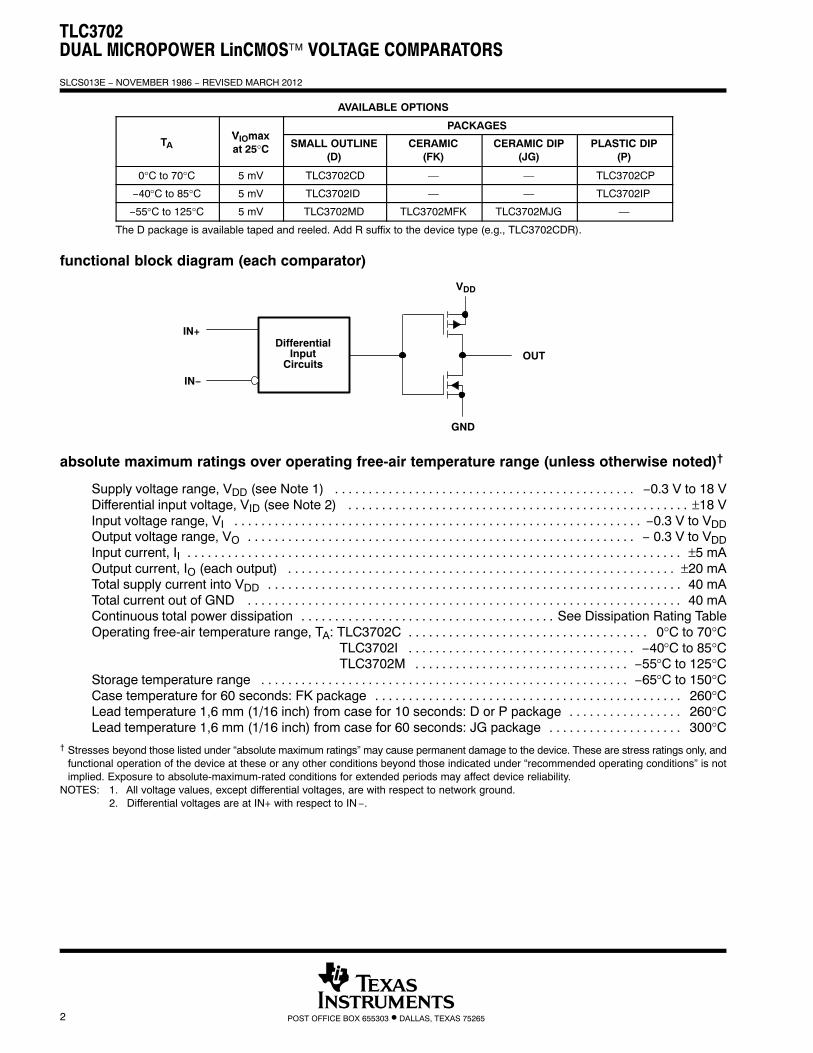
functional block diagram (each comparator)
VDD
GND
OUTDifferential
InputCircuits
IN+
IN−
absolute maximum ratings over operating free-air temperature range (unless otherwise noted)†
Supply voltage range, VDD (see Note 1) −0.3 V to 18 V. . . . . . . . . . . . . . . . . . . . . . . . . . . . . . . . . . . . . . . . . . . . . Differential input voltage, VID (see Note 2) ±18 V. . . . . . . . . . . . . . . . . . . . . . . . . . . . . . . . . . . . . . . . . . . . . . . . . . . Input voltage range, VI −0.3 V to VDD. . . . . . . . . . . . . . . . . . . . . . . . . . . . . . . . . . . . . . . . . . . . . . . . . . . . . . . . . . . . . Output voltage range, VO − 0.3 V to VDD. . . . . . . . . . . . . . . . . . . . . . . . . . . . . . . . . . . . . . . . . . . . . . . . . . . . . . . . . . Input current, II ±5 mA. . . . . . . . . . . . . . . . . . . . . . . . . . . . . . . . . . . . . . . . . . . . . . . . . . . . . . . . . . . . . . . . . . . . . . . . . . Output current, IO (each output) ±20 mA. . . . . . . . . . . . . . . . . . . . . . . . . . . . . . . . . . . . . . . . . . . . . . . . . . . . . . . . . . Total supply current into VDD 40 mA. . . . . . . . . . . . . . . . . . . . . . . . . . . . . . . . . . . . . . . . . . . . . . . . . . . . . . . . . . . . . . Total current out of GND 40 mA. . . . . . . . . . . . . . . . . . . . . . . . . . . . . . . . . . . . . . . . . . . . . . . . . . . . . . . . . . . . . . . . . Continuous total power dissipation See Dissipation Rating Table. . . . . . . . . . . . . . . . . . . . . . . . . . . . . . . . . . . . . . Operating free-air temperature range, TA: TLC3702C 0°C to 70°C. . . . . . . . . . . . . . . . . . . . . . . . . . . . . . . . . . . .
TLC3702I −40°C to 85°C. . . . . . . . . . . . . . . . . . . . . . . . . . . . . . . . . . TLC3702M −55°C to 125°C. . . . . . . . . . . . . . . . . . . . . . . . . . . . . . . .
Storage temperature range −65°C to 150°C. . . . . . . . . . . . . . . . . . . . . . . . . . . . . . . . . . . . . . . . . . . . . . . . . . . . . . . Case temperature for 60 seconds: FK package 260°C. . . . . . . . . . . . . . . . . . . . . . . . . . . . . . . . . . . . . . . . . . . . . . Lead temperature 1,6 mm (1/16 inch) from case for 10 seconds: D or P package 260°C. . . . . . . . . . . . . . . . . Lead temperature 1,6 mm (1/16 inch) from case for 60 seconds: JG package 300°C. . . . . . . . . . . . . . . . . . . .
† Stresses beyond those listed under “absolute maximum ratings” may cause permanent damage to the device. These are stress ratings only, andfunctional operation of the device at these or any other conditions beyond those indicated under “recommended operating conditions” is notimplied. Exposure to absolute-maximum-rated conditions for extended periods may affect device reliability.
NOTES: 1. All voltage values, except differential voltages, are with respect to network ground.2. Differential voltages are at IN+ with respect to IN−.
TLC3702DUAL MICROPOWER LinCMOS™ VOLTAGE COMPARATORS
SLCS013E − NOVEMBER 1986 − REVISED MARCH 2012
3POST OFFICE BOX 655303 • DALLAS, TEXAS 75265
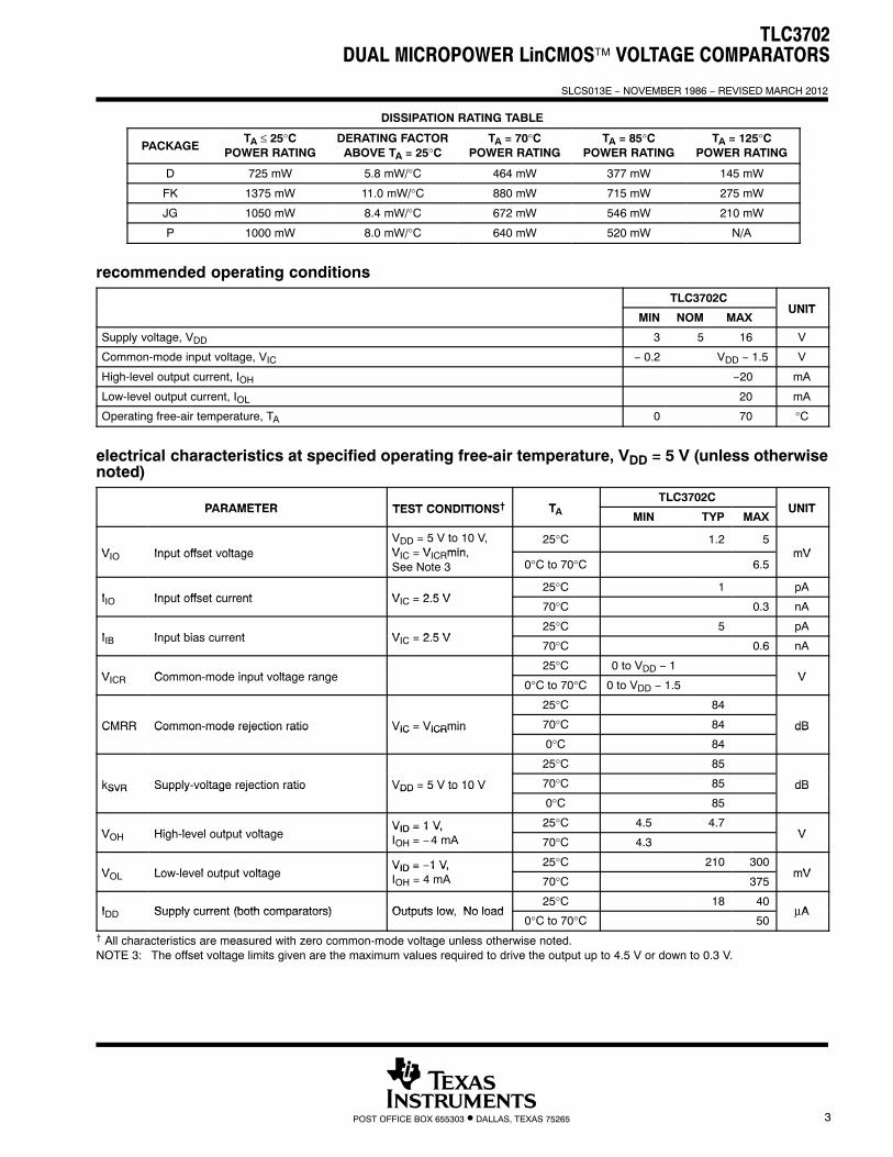
DISSIPATION RATING TABLE
PACKAGETA ≤ 25°C
POWER RATINGDERATING FACTOR
ABOVE TA = 25°CTA = 70°C
POWER RATINGTA = 85°C
POWER RATINGTA = 125°C
POWER RATING
D 725 mW 5.8 mW/°C 464 mW 377 mW 145 mW
FK 1375 mW 11.0 mW/°C 880 mW 715 mW 275 mW
JG 1050 mW 8.4 mW/°C 672 mW 546 mW 210 mW
P 1000 mW 8.0 mW/°C 640 mW 520 mW N/A
recommended operating conditions
TLC3702CUNIT
MIN NOM MAXUNIT
Supply voltage, VDD 3 5 16 V
Common-mode input voltage, VIC − 0.2 VDD − 1.5 V
High-level output current, IOH −20 mA
Low-level output current, IOL 20 mA
Operating free-air temperature, TA 0 70 °C
electrical characteristics at specified operating free-air temperature, VDD = 5 V (unless otherwisenoted)
PARAMETER TEST CONDITIONS† TTLC3702C
UNITPARAMETER TEST CONDITIONS† TA MIN TYP MAXUNIT
V Input offset voltageVDD = 5 V to 10 V,V V min
25°C 1.2 5mVVIO Input offset voltage VIC = VICRmin,
See Note 3 0°C to 70°C 6.5mV
I Input offset current V 2 5 V25°C 1 pA
IIO Input offset current VIC = 2.5 V70°C 0.3 nA
I Input bias current V 2 5 V25°C 5 pA
IIB Input bias current VIC = 2.5 V70°C 0.6 nA
V Common mode input voltage range25°C 0 to VDD − 1
VVICR Common-mode input voltage range0°C to 70°C 0 to VDD − 1.5
V
25°C 84
CMRR Common-mode rejection ratio VIC = VICRmin 70°C 84 dBCMRR Common mode rejection ratio VIC VICRmin
0°C 84
dB
25°C 85
kSVR Supply-voltage rejection ratio VDD = 5 V to 10 V 70°C 85 dBkSVR Supply voltage rejection ratio VDD 5 V to 10 V
0°C 85
dB
V High level output voltageVID = 1 V, 25°C 4.5 4.7
VVOH High-level output voltageVID = 1 V,IOH = −4 mA 70°C 4.3
V
V Low level output voltageVID = −1 V, 25°C 210 300
mVVOL Low-level output voltageVID = 1 V,IOH = 4 mA 70°C 375
mV
I Supply current (both comparators) Outputs low No load25°C 18 40
μAIDD Supply current (both comparators) Outputs low, No load0°C to 70°C 50
μA
† All characteristics are measured with zero common-mode voltage unless otherwise noted.NOTE 3: The offset voltage limits given are the maximum values required to drive the output up to 4.5 V or down to 0.3 V.
TLC3702DUAL MICROPOWER LinCMOS™ VOLTAGE COMPARATORS
SLCS013E − NOVEMBER 1986 − REVISED MARCH 2012
4 POST OFFICE BOX 655303 • DALLAS, TEXAS 75265
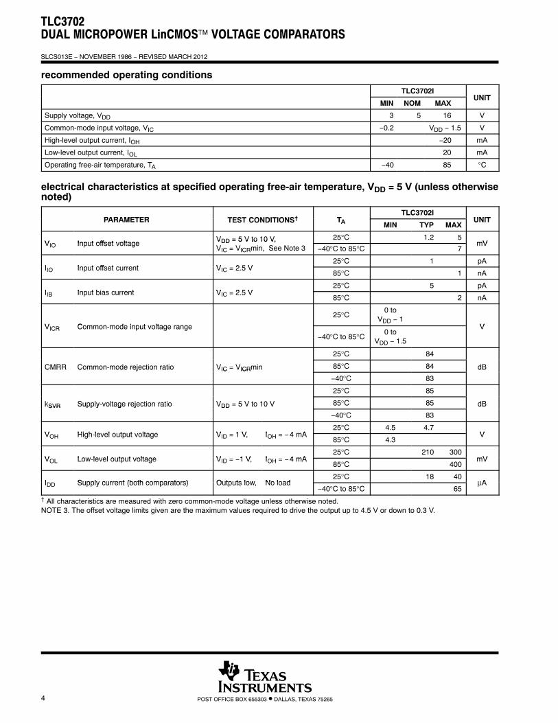
recommended operating conditions
TLC3702IUNIT
MIN NOM MAXUNIT
Supply voltage, VDD 3 5 16 V
Common-mode input voltage, VIC −0.2 VDD − 1.5 V
High-level output current, IOH −20 mA
Low-level output current, IOL 20 mA
Operating free-air temperature, TA −40 85 °C
electrical characteristics at specified operating free-air temperature, VDD = 5 V (unless otherwisenoted)
PARAMETER TEST CONDITIONS† TTLC3702I
UNITPARAMETER TEST CONDITIONS† TA MIN TYP MAXUNIT
V Input offset voltageVDD = 5 V to 10 V, 25°C 1.2 5
mVVIO Input offset voltageVDD = 5 V to 10 V,VIC = VICRmin, See Note 3 −40°C to 85°C 7
mV
I Input offset current V 2 5 V25°C 1 pA
IIO Input offset current VIC = 2.5 V85°C 1 nA
I Input bias current V 2 5 V25°C 5 pA
IIB Input bias current VIC = 2.5 V85°C 2 nA
V Common mode input voltage range
25°C0 to
VDD − 1VVICR Common-mode input voltage range
−40°C to 85°C0 to
VDD − 1.5
V
25°C 84
CMRR Common-mode rejection ratio VIC = VICRmin 85°C 84 dBCMRR Common mode rejection ratio VIC VICRmin
−40°C 83
dB
25°C 85
kSVR Supply-voltage rejection ratio VDD = 5 V to 10 V 85°C 85 dBkSVR Supply voltage rejection ratio VDD 5 V to 10 V
−40°C 83
dB
V High level output voltage V 1 V I 4 mA25°C 4.5 4.7
VVOH High-level output voltage VID = 1 V, IOH = −4 mA85°C 4.3
V
V Low level output voltage V 1 V I 4 mA25°C 210 300
mVVOL Low-level output voltage VID = −1 V, IOH = −4 mA85°C 400
mV
I Supply current (both comparators) Outputs low No load25°C 18 40
μAIDD Supply current (both comparators) Outputs low, No load−40°C to 85°C 65
μA
† All characteristics are measured with zero common-mode voltage unless otherwise noted.NOTE 3. The offset voltage limits given are the maximum values required to drive the output up to 4.5 V or down to 0.3 V.
TLC3702DUAL MICROPOWER LinCMOS™ VOLTAGE COMPARATORS
SLCS013E − NOVEMBER 1986 − REVISED MARCH 2012
5POST OFFICE BOX 655303 • DALLAS, TEXAS 75265
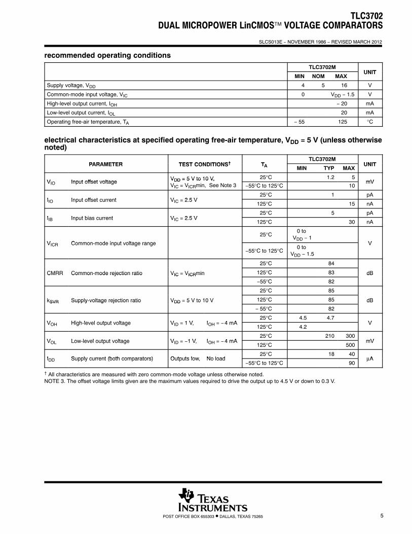
recommended operating conditions
TLC3702MUNIT
MIN NOM MAXUNIT
Supply voltage, VDD 4 5 16 V
Common-mode input voltage, VIC 0 VDD − 1.5 V
High-level output current, IOH − 20 mA
Low-level output current, IOL 20 mA
Operating free-air temperature, TA − 55 125 °C
electrical characteristics at specified operating free-air temperature, VDD = 5 V (unless otherwisenoted)
PARAMETER TEST CONDITIONS† TTLC3702M
UNITPARAMETER TEST CONDITIONS† TA MIN TYP MAXUNIT
V Input offset voltageVDD = 5 V to 10 V, 25°C 1.2 5
mVVIO Input offset voltageVDD = 5 V to 10 V,VIC = VICRmin, See Note 3 −55°C to 125°C 10
mV
I Input offset current V 2 5 V25°C 1 pA
IIO Input offset current VIC = 2.5 V125°C 15 nA
I Input bias current V 2 5 V25°C 5 pA
IIB Input bias current VIC = 2.5 V125°C 30 nA
V Common mode input voltage range
25°C0 to
VDD − 1VVICR Common-mode input voltage range
−55°C to 125°C0 to
VDD − 1.5
V
25°C 84
CMRR Common-mode rejection ratio VIC = VICRmin 125°C 83 dBCMRR Common mode rejection ratio VIC VICRmin
−55°C 82
dB
25°C 85
kSVR Supply-voltage rejection ratio VDD = 5 V to 10 V 125°C 85 dBkSVR Supply voltage rejection ratio VDD 5 V to 10 V
− 55°C 82
dB
V High level output voltage V 1 V I 4 mA25°C 4.5 4.7
VVOH High-level output voltage VID = 1 V, IOH = −4 mA125°C 4.2
V
V Low level output voltage V 1 V I 4 mA25°C 210 300
mVVOL Low-level output voltage VID = −1 V, IOH = −4 mA125°C 500
mV
I Supply current (both comparators) Outputs low No load25°C 18 40
μAIDD Supply current (both comparators) Outputs low, No load−55°C to 125°C 90
μA
† All characteristics are measured with zero common-mode voltage unless otherwise noted.NOTE 3. The offset voltage limits given are the maximum values required to drive the output up to 4.5 V or down to 0.3 V.

TLC3702DUAL MICROPOWER LinCMOS™ VOLTAGE COMPARATORS
SLCS013E − NOVEMBER 1986 − REVISED MARCH 2012
6 POST OFFICE BOX 655303 • DALLAS, TEXAS 75265
switching characteristics, VDD = 5 V, TA = 25°C
PARAMETER TEST CONDITIONS
TLC3702C, TLC3702ITLC3702M UNITPARAMETER TEST CONDITIONS
MIN TYP MAXUNIT
Overdrive = 2 mV 4.5
f 10 kHOverdrive = 5 mV 2.7
tPLH Propagation delay time, low-to-high-level output†f = 10 kHz,CL = 50 pF
Overdrive = 10 mV 1.9 μstPLH Propagation delay time, low to high level output CL = 50 pFOverdrive = 20 mV 1.4
μs
Overdrive = 40 mV 1.1
VI = 1.4 V step at IN+ 1.1
Overdrive = 2 mV 4
f 10 kHOverdrive = 5 mV 2.3
tPHL Propagation delay time, high-to-low-level output†f = 10 kHz,CL = 50 pF
Overdrive = 10 mV 1.5 μstPHL Propagation delay time, high to low level output CL = 50 pFOverdrive = 20 mV 0.95
μs
Overdrive = 40 mV 0.65
VI = 1.4 V step at IN+ 0.15
tf Fall timef = 10 kHz,CL = 50 pF
Overdrive = 50 mV 50 ns
tr Rise timef = 10 kHz,CL = 50 pF
Overdrive = 50 mV 125 ns
† Simultaneous switching of inputs causes degradation in output response.
LinCMOS and Advanced LinCMOS are trademarks of Texas Instruments Incorporated.
TLC3702DUAL MICROPOWER LinCMOS™ VOLTAGE COMPARATORS
SLCS013E − NOVEMBER 1986 − REVISED MARCH 2012
7POST OFFICE BOX 655303 • DALLAS, TEXAS 75265
PRINCIPLES OF OPERATION
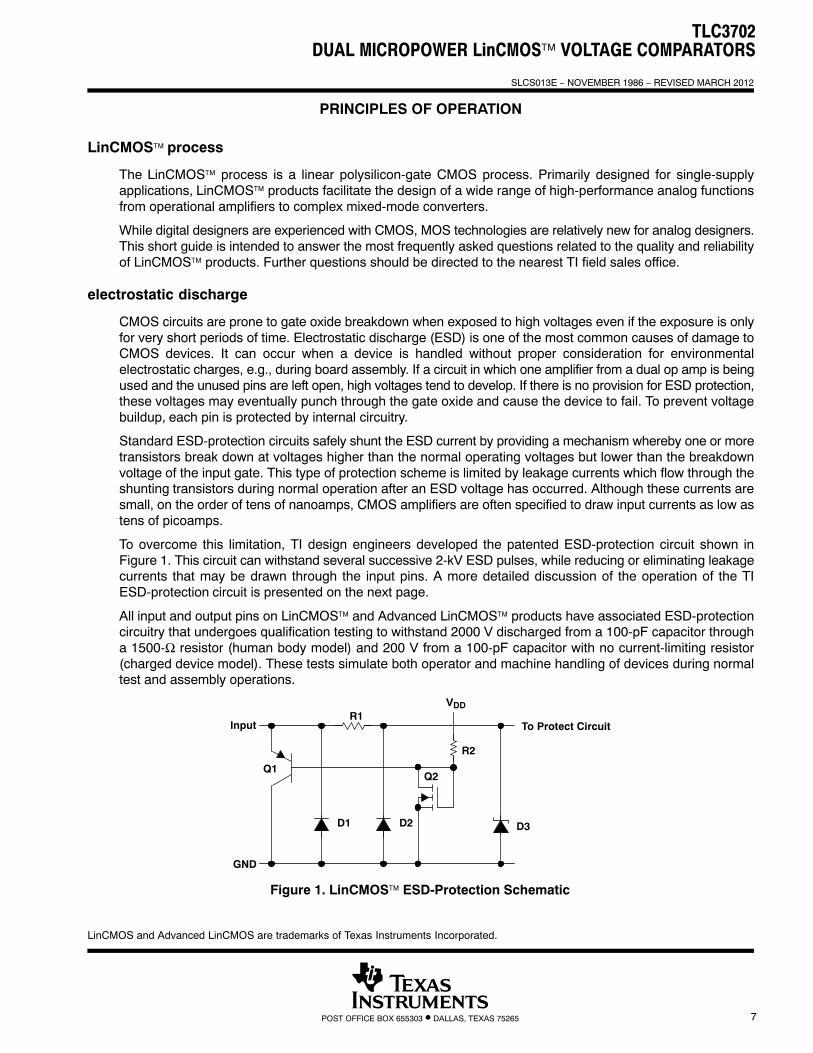
LinCMOS™ process
The LinCMOS™ process is a linear polysilicon-gate CMOS process. Primarily designed for single-supplyapplications, LinCMOS™ products facilitate the design of a wide range of high-performance analog functionsfrom operational amplifiers to complex mixed-mode converters.
While digital designers are experienced with CMOS, MOS technologies are relatively new for analog designers.This short guide is intended to answer the most frequently asked questions related to the quality and reliabilityof LinCMOS™ products. Further questions should be directed to the nearest TI field sales office.
electrostatic discharge
CMOS circuits are prone to gate oxide breakdown when exposed to high voltages even if the exposure is onlyfor very short periods of time. Electrostatic discharge (ESD) is one of the most common causes of damage toCMOS devices. It can occur when a device is handled without proper consideration for environmentalelectrostatic charges, e.g., during board assembly. If a circuit in which one amplifier from a dual op amp is beingused and the unused pins are left open, high voltages tend to develop. If there is no provision for ESD protection,these voltages may eventually punch through the gate oxide and cause the device to fail. To prevent voltagebuildup, each pin is protected by internal circuitry.
Standard ESD-protection circuits safely shunt the ESD current by providing a mechanism whereby one or moretransistors break down at voltages higher than the normal operating voltages but lower than the breakdownvoltage of the input gate. This type of protection scheme is limited by leakage currents which flow through theshunting transistors during normal operation after an ESD voltage has occurred. Although these currents aresmall, on the order of tens of nanoamps, CMOS amplifiers are often specified to draw input currents as low astens of picoamps.
To overcome this limitation, TI design engineers developed the patented ESD-protection circuit shown inFigure 1. This circuit can withstand several successive 2-kV ESD pulses, while reducing or eliminating leakagecurrents that may be drawn through the input pins. A more detailed discussion of the operation of the TIESD-protection circuit is presented on the next page.
All input and output pins on LinCMOS™ and Advanced LinCMOS™ products have associated ESD-protectioncircuitry that undergoes qualification testing to withstand 2000 V discharged from a 100-pF capacitor througha 1500-Ω resistor (human body model) and 200 V from a 100-pF capacitor with no current-limiting resistor(charged device model). These tests simulate both operator and machine handling of devices during normaltest and assembly operations.
To Protect Circuit
D3
R2
Q2
D2D1
Q1
Input
GND
R1VDD
Figure 1. LinCMOS™ ESD-Protection Schematic
TLC3702DUAL MICROPOWER LinCMOS™ VOLTAGE COMPARATORS
SLCS013E − NOVEMBER 1986 − REVISED MARCH 2012
8 POST OFFICE BOX 655303 • DALLAS, TEXAS 75265
PRINCIPLES OF OPERATION
input protection circuit operation
Texas Instruments patented protection circuitry allows for both positive- and negative-going ESD transients.These transients are characterized by extremely fast rise times and usually low energies, and can occur bothwhen the device has all pins open and when it is installed in a circuit.
positive ESD transients
Initial positive charged energy is shunted through Q1 to VSS. Q1 turns on when the voltage at the input risesabove the voltage on the VDD pin by a value equal to the VBE of Q1. The base current increases through R2with input current as Q1 saturates. The base current through R2 forces the voltage at the drain and gate of Q2to exceed its threshold level (VT ∼ 22 to 26 V) and turn Q2 on. The shunted input current through Q1 to VSS isnow shunted through the n-channel enhancement-type MOSFET Q2 to VSS. If the voltage on the input pincontinues to rise, the breakdown voltage of the zener diode D3 is exceeded and all remaining energy isdissipated in R1 and D3. The breakdown voltage of D3 is designed to be 24 V to 27 V, which is well below thegate-oxide voltage of the circuit to be protected.
negative ESD transients
The negative charged ESD transients are shunted directly through D1. Additional energy is dissipated in R1and D2 as D2 becomes forward biased. The voltage seen by the protected circuit is −0.3 V to −1 V (the forwardvoltage of D1 and D2).
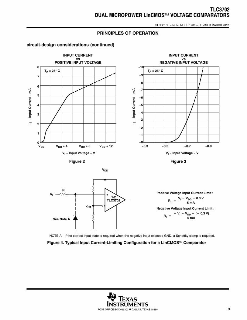
circuit-design considerations
LinCMOS™ products are being used in actual circuit environments that have input voltages that exceed therecommended common-mode input voltage range and activate the input protection circuit. Even under normaloperation, these conditions occur during circuit power up or power down, and in many cases, when the deviceis being used for a signal conditioning function. The input voltages can exceed VICR and not damage the deviceonly if the inputs are current limited. The recommended current limit shown on most product data sheets is±5 mA. Figure 2 and Figure 3 show typical characteristics for input voltage versus input current.
Normal operation and correct output state can be expected even when the input voltage exceeds the positivesupply voltage. Again, the input current should be externally limited even though internal positive current limitingis achieved in the input protection circuit by the action of Q1. When Q1 is on, it saturates and limits the currentto approximately 5-mA collector current by design. When saturated, Q1 base current increases with inputcurrent. This base current is forced into the VDD pin and into the device IDD or the VDD supply through R2producing the current limiting effects shown in Figure 2. This internal limiting lasts only as long as the inputvoltage is below the VT of Q2.
When the input voltage exceeds the negative supply voltage, normal operation is affected and output voltagestates may not be correct. Also, the isolation between channels of multiple devices (duals and quads) can beseverely affected. External current limiting must be used since this current is directly shunted by D1 and D2 andno internal limiting is achieved. If normal output voltage states are required, an external input voltage clamp isrequired (see Figure 4).
TLC3702DUAL MICROPOWER LinCMOS™ VOLTAGE COMPARATORS
SLCS013E − NOVEMBER 1986 − REVISED MARCH 2012
9POST OFFICE BOX 655303 • DALLAS, TEXAS 75265
PRINCIPLES OF OPERATION
circuit-design considerations (continued)
Figure 2
VDD VDD + 4 VDD + 8 VDD + 12
INPUT CURRENTvs
POSITIVE INPUT VOLTAGE
TA = 25° C8
7
6
5
4
3
2
1
0
VI − Input Voltage − V
− In
pu
t C
urr
ent −
mA
I I
Figure 3
−0.3
VI − Input Voltage − V
INPUT CURRENTvs
NEGATIVE INPUT VOLTAGE
TA = 25° C
−0.5 −0.7 −0.9
−10
−9
−8
−7
−6
−5
−4
−3
−2
−1
−0
− In
pu
t C
urr
ent −
mA
I I
+
−
1/2TLC3702
Vref
VI
VDD
See Note A
RI
NOTE A: If the correct input state is required when the negative input exceeds GND, a Schottky clamp is required.
Negative Voltage Input Current Limit :
RI �
� VI � VDD � (� 0.3 V)5 mA
RI �
VI � VDD � 0.3 V5 mA
Positive Voltage Input Current Limit :
Figure 4. Typical Input Current-Limiting Configuration for a LinCMOS™ Comparator
TLC3702DUAL MICROPOWER LinCMOS™ VOLTAGE COMPARATORS
SLCS013E − NOVEMBER 1986 − REVISED MARCH 2012
10 POST OFFICE BOX 655303 • DALLAS, TEXAS 75265
PARAMETER MEASUREMENT INFORMATION
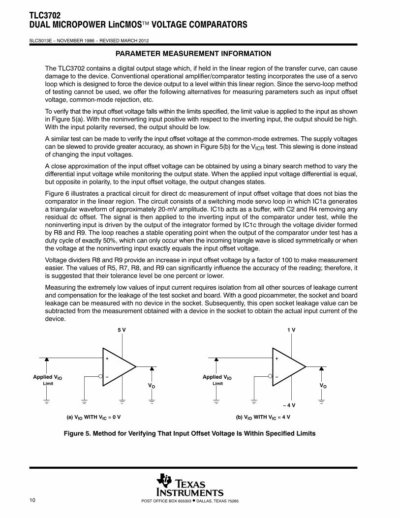
The TLC3702 contains a digital output stage which, if held in the linear region of the transfer curve, can causedamage to the device. Conventional operational amplifier/comparator testing incorporates the use of a servoloop which is designed to force the device output to a level within this linear region. Since the servo-loop methodof testing cannot be used, we offer the following alternatives for measuring parameters such as input offsetvoltage, common-mode rejection, etc.
To verify that the input offset voltage falls within the limits specified, the limit value is applied to the input as shownin Figure 5(a). With the noninverting input positive with respect to the inverting input, the output should be high.With the input polarity reversed, the output should be low.
A similar test can be made to verify the input offset voltage at the common-mode extremes. The supply voltagescan be slewed to provide greater accuracy, as shown in Figure 5(b) for the VICR test. This slewing is done insteadof changing the input voltages.
A close approximation of the input offset voltage can be obtained by using a binary search method to vary thedifferential input voltage while monitoring the output state. When the applied input voltage differential is equal,but opposite in polarity, to the input offset voltage, the output changes states.
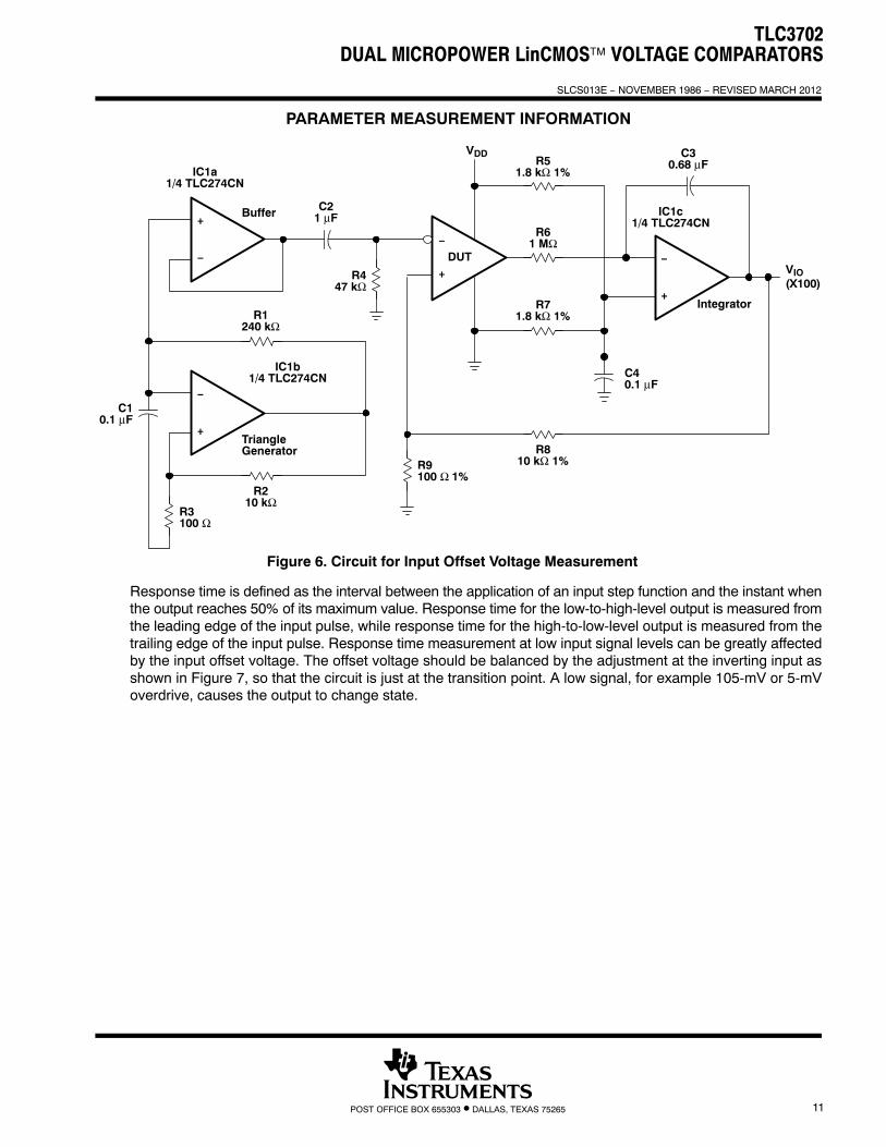
Figure 6 illustrates a practical circuit for direct dc measurement of input offset voltage that does not bias thecomparator in the linear region. The circuit consists of a switching mode servo loop in which IC1a generatesa triangular waveform of approximately 20-mV amplitude. IC1b acts as a buffer, with C2 and R4 removing anyresidual dc offset. The signal is then applied to the inverting input of the comparator under test, while thenoninverting input is driven by the output of the integrator formed by IC1c through the voltage divider formedby R8 and R9. The loop reaches a stable operating point when the output of the comparator under test has aduty cycle of exactly 50%, which can only occur when the incoming triangle wave is sliced symmetrically or whenthe voltage at the noninverting input exactly equals the input offset voltage.
Voltage dividers R8 and R9 provide an increase in input offset voltage by a factor of 100 to make measurementeasier. The values of R5, R7, R8, and R9 can significantly influence the accuracy of the reading; therefore, itis suggested that their tolerance level be one percent or lower.
Measuring the extremely low values of input current requires isolation from all other sources of leakage currentand compensation for the leakage of the test socket and board. With a good picoammeter, the socket and boardleakage can be measured with no device in the socket. Subsequently, this open socket leakage value can besubtracted from the measurement obtained with a device in the socket to obtain the actual input current of thedevice.
+
−
5 V
Applied VIO Limit VO
+
−
1 V
Applied VIO Limit VO
− 4 V
(a) VIO WITH VIC = 0 V (b) VIO WITH VIC = 4 V
Figure 5. Method for Verifying That Input Offset Voltage Is Within Specified Limits
TLC3702DUAL MICROPOWER LinCMOS™ VOLTAGE COMPARATORS
SLCS013E − NOVEMBER 1986 − REVISED MARCH 2012
11POST OFFICE BOX 655303 • DALLAS, TEXAS 75265
PARAMETER MEASUREMENT INFORMATION
−
+DUT
VDD
+
−
−
+
−
+
C21 μF
R447 kΩ
R51.8 kΩ 1%
C30.68 μF
IC1c1/4 TLC274CN
IC1a1/4 TLC274CN
IC1b1/4 TLC274CN
R61 MΩ
R71.8 kΩ 1%
R810 kΩ 1%
R1240 kΩ
R210 kΩ
C10.1 μF
R3100 Ω
C40.1 μF
Integrator
R9100 Ω 1%
Buffer
TriangleGenerator
VIO(X100)
Figure 6. Circuit for Input Offset Voltage Measurement
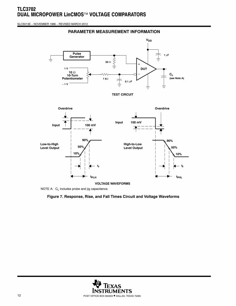
Response time is defined as the interval between the application of an input step function and the instant whenthe output reaches 50% of its maximum value. Response time for the low-to-high-level output is measured fromthe leading edge of the input pulse, while response time for the high-to-low-level output is measured from thetrailing edge of the input pulse. Response time measurement at low input signal levels can be greatly affectedby the input offset voltage. The offset voltage should be balanced by the adjustment at the inverting input asshown in Figure 7, so that the circuit is just at the transition point. A low signal, for example 105-mV or 5-mVoverdrive, causes the output to change state.
TLC3702DUAL MICROPOWER LinCMOS™ VOLTAGE COMPARATORS
SLCS013E − NOVEMBER 1986 − REVISED MARCH 2012
12 POST OFFICE BOX 655303 • DALLAS, TEXAS 75265
PARAMETER MEASUREMENT INFORMATION
+
−
DUT
VDD
CL(see Note A)
PulseGenerator
10 Ω 10-Turn
Potentiometer
1 V
− 1 V
1 kΩ
50 Ω
1 μF
0.1 μF
TEST CIRCUIT
100 mVInput
Overdrive
90%
50%
10%
tr
tPLH
100 mVInput
Overdrive
90%
50%
10%
tf
tPHL
Low-to-HighLevel Output
High-to-LowLevel Output
VOLTAGE WAVEFORMS
NOTE A: CL includes probe and jig capacitance.
Figure 7. Response, Rise, and Fall Times Circuit and Voltage Waveforms
TLC3702DUAL MICROPOWER LinCMOS™ VOLTAGE COMPARATORS
SLCS013E − NOVEMBER 1986 − REVISED MARCH 2012
13POST OFFICE BOX 655303 • DALLAS, TEXAS 75265
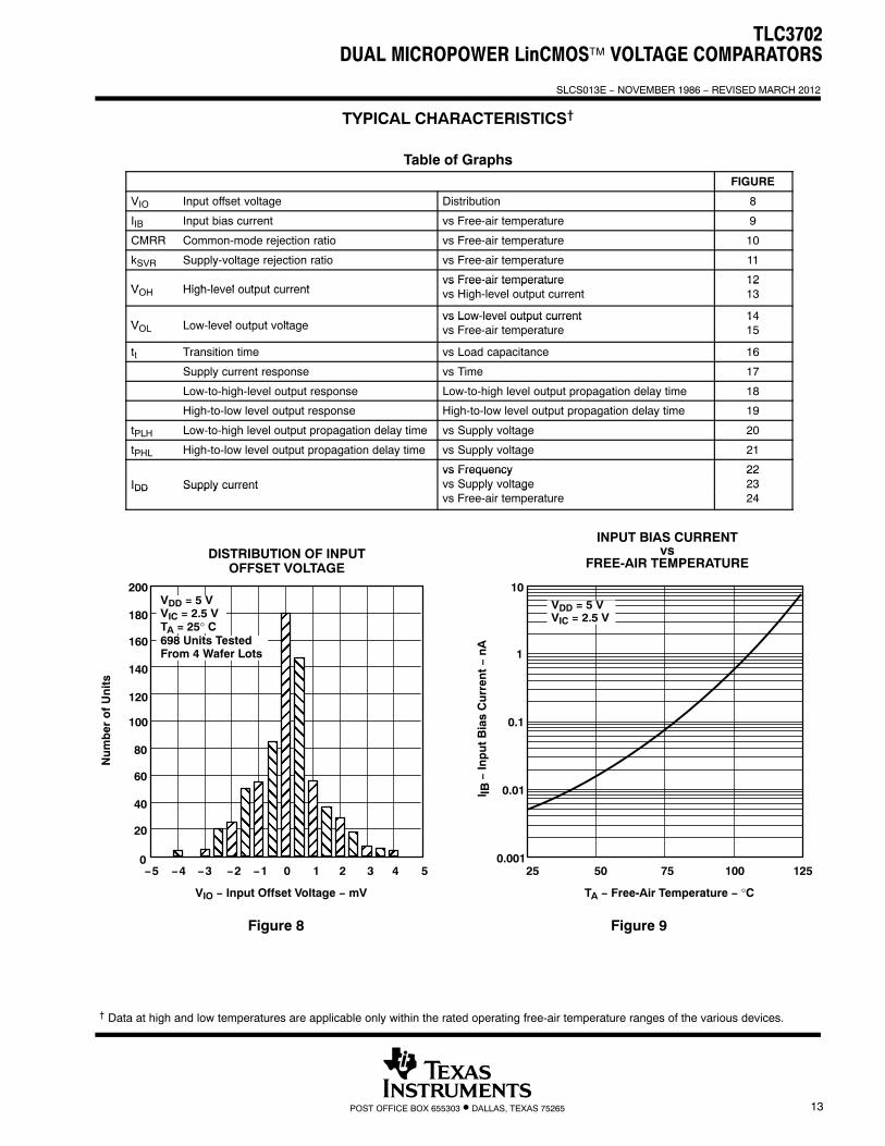
TYPICAL CHARACTERISTICS†
Table of GraphsFIGURE
VIO Input offset voltage Distribution 8
IIB Input bias current vs Free-air temperature 9
CMRR Common-mode rejection ratio vs Free-air temperature 10
kSVR Supply-voltage rejection ratio vs Free-air temperature 11
V High level output currentvs Free-air temperature 12
VOH High-level output currentvs Free air temperaturevs High-level output current
1213
V Low level output voltagevs Low-level output current 14
VOL Low-level output voltagevs Low level output currentvs Free-air temperature
1415
tt Transition time vs Load capacitance 16
Supply current response vs Time 17
Low-to-high-level output response Low-to-high level output propagation delay time 18
High-to-low level output response High-to-low level output propagation delay time 19
tPLH Low-to-high level output propagation delay time vs Supply voltage 20
tPHL High-to-low level output propagation delay time vs Supply voltage 21
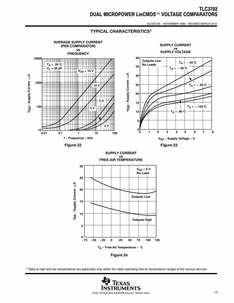
vs Frequency 22IDD Supply current
vs Frequencyvs Supply voltage
2223IDD Supply current vs Supply voltage
vs Free-air temperature2324
Figure 8
ÉÇÇÇÇ
ÇÇÇÇÇÇÇÇÉÉ
ÉÉÉÉÉÉÉÉÉÉÉÉÉÉÉÉÉÉÉÉÉÉÉÉ
ÇÇÇÇÇÇÇÇÇÇ
ÇÇÇÇÇÇ
ÉÉÉÉ
ÇÇÇÇÉÉÇÇ
ÇÇÇ
ÉÉÉ
ÉÉÉÉÉÉÉÉÇÇ
Nu
mb
er o
f U
nit
s
VDD = 5 VVIC = 2.5 VTA = 25° C
−5 −4 −3 −2 −1 0 1 2 3 4 5
VIO − Input Offset Voltage − mV
DISTRIBUTION OF INPUTOFFSET VOLTAGE
200
180
160
140
120
100
80
60
40
20
0
698 Units TestedFrom 4 Wafer Lots
Figure 9
I
TA − Free-Air Temperature − °C
IB −
Inp
ut
Bia
s C
urr
ent −
nA
25 50 75 100 125
10
1
0.1
0.01
0.001
INPUT BIAS CURRENTvs
FREE-AIR TEMPERATURE
VDD = 5 VVIC = 2.5 V
† Data at high and low temperatures are applicable only within the rated operating free-air temperature ranges of the various devices.
TLC3702DUAL MICROPOWER LinCMOS™ VOLTAGE COMPARATORS
SLCS013E − NOVEMBER 1986 − REVISED MARCH 2012
14 POST OFFICE BOX 655303 • DALLAS, TEXAS 75265
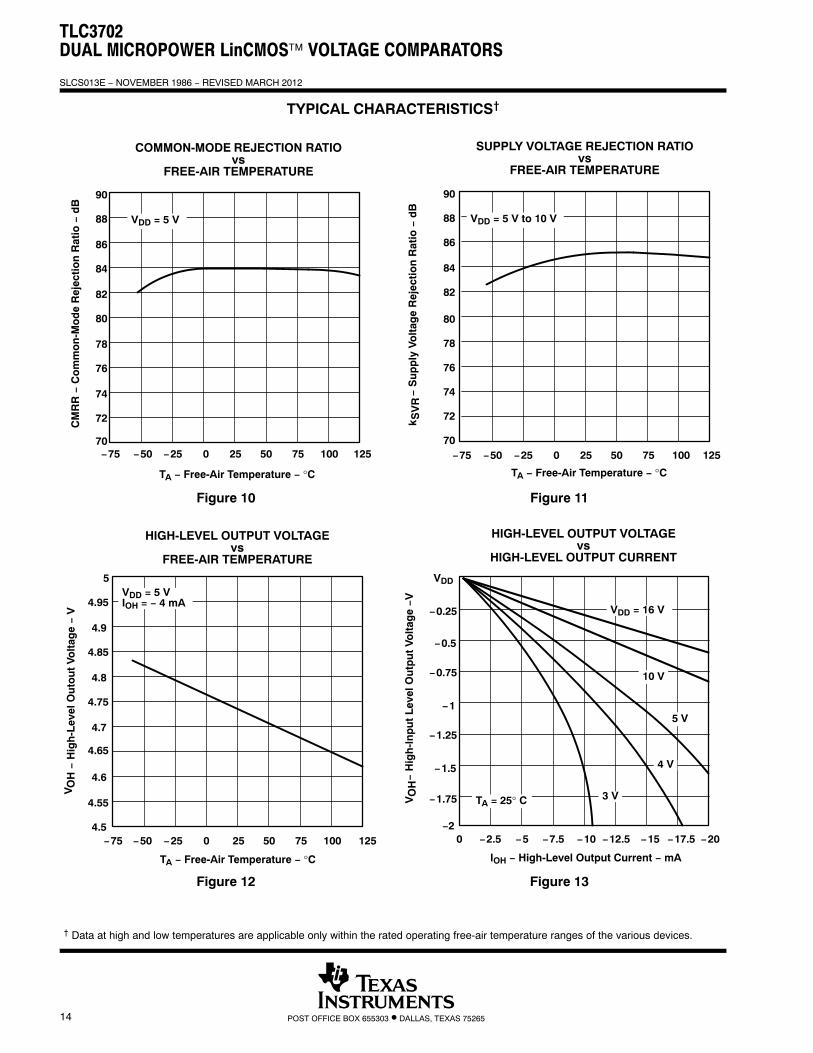
TYPICAL CHARACTERISTICS†
Figure 10
CM
RR
− C
om
mo
n-M
od
e R
ejec
tio
n R
atio
− d
B
TA − Free-Air Temperature − °C
COMMON-MODE REJECTION RATIOvs
FREE-AIR TEMPERATURE
−75 −50 −25 0 25 50 75 100 125
VDD = 5 V
90
88
86
84
82
80
78
76
74
72
70
Figure 11
−75 −50 −25 0 25 50 75 100 125
k SV
R −
Su
pp
ly V
olt
age
Rej
ecti
on
Rat
io −
dB
TA − Free-Air Temperature − °C
SUPPLY VOLTAGE REJECTION RATIOvs
FREE-AIR TEMPERATURE
VDD = 5 V to 10 V
90
88
86
84
82
80
78
76
74
72
70
Figure 12
5
TA − Free-Air Temperature − °C
HIGH-LEVEL OUTPUT VOLTAGEvs
FREE-AIR TEMPERATURE
VO
H −
Hig
h-L
evel
Ou
tou
t Vo
ltag
e −
V
VDD = 5 VIOH = − 4 mA
−75 −50 −25 0 25 50 75 100 125
4.9
4.8
4.7
4.6
4.5
4.55
4.65
4.75
4.85
4.95
Figure 13
VDD = 16 V
IOH − High-Level Output Current − mA
HIGH-LEVEL OUTPUT VOLTAGEvs
HIGH-LEVEL OUTPUT CURRENT
VO
H
TA = 25° C 3 V
4 V
5 V
10 V
0 −2.5 −5 −7.5 −10 −12.5 −15 −17.5 −20
− H
igh
-In
pu
t L
evel
Ou
tpu
t Vo
ltag
e −V
VDD
−0.25
−0.5
−0.75
−1
−1.25
−1.5
−1.75
−2
† Data at high and low temperatures are applicable only within the rated operating free-air temperature ranges of the various devices.
TLC3702DUAL MICROPOWER LinCMOS™ VOLTAGE COMPARATORS
SLCS013E − NOVEMBER 1986 − REVISED MARCH 2012
15POST OFFICE BOX 655303 • DALLAS, TEXAS 75265
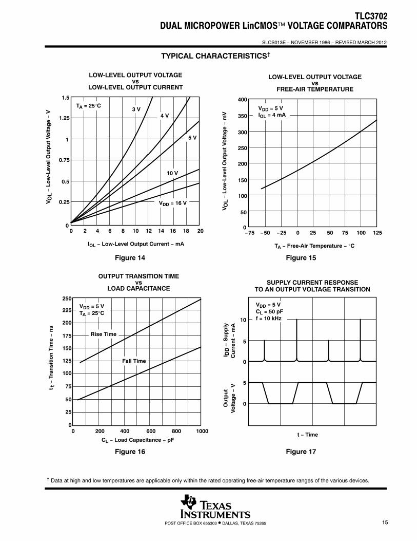
TYPICAL CHARACTERISTICS†
Figure 14
IOL − Low-Level Output Current − mA
0 2 4 6 8 10 12 14 16 18 20
VO
L −
Lo
w-L
evel
Ou
tpu
t Vo
ltag
e −
V
LOW-LEVEL OUTPUT VOLTAGEvs
LOW-LEVEL OUTPUT CURRENT
3 V4 V
10 V
VDD = 16 V
5 V
1.5
1.25
1
0.75
0.5
0.25
0
TA = 25°C
Figure 15
−75 −50 −25 0 25 50 75 100 125
TA − Free-Air Temperature − °C
LOW-LEVEL OUTPUT VOLTAGEvs
FREE-AIR TEMPERATURE
VO
L −
Lo
w-L
evel
Ou
tpu
t Vo
ltag
e −
mV
400
350
300
250
200
150
100
50
0
VDD = 5 VIOL = 4 mA
Figure 16
0 200 400 600 800 1000
CL − Load Capacitance − pF
t t −
Tra
nsi
tio
n T
ime −
ns
OUTPUT TRANSITION TIMEvs
LOAD CAPACITANCE
250
225
200
175
150
125
100
75
50
25
0
VDD = 5 VTA = 25°C
Rise Time
Fall Time
Figure 17
I DD
− S
up
ply
SUPPLY CURRENT RESPONSETO AN OUTPUT VOLTAGE TRANSITION
Cu
rren
t −
mA
t − Time
Ou
tpu
tV
olt
age −
V
10
5
0
5
0
VDD = 5 VCL = 50 pFf = 10 kHz
† Data at high and low temperatures are applicable only within the rated operating free-air temperature ranges of the various devices.
TLC3702DUAL MICROPOWER LinCMOS™ VOLTAGE COMPARATORS
SLCS013E − NOVEMBER 1986 − REVISED MARCH 2012
16 POST OFFICE BOX 655303 • DALLAS, TEXAS 75265
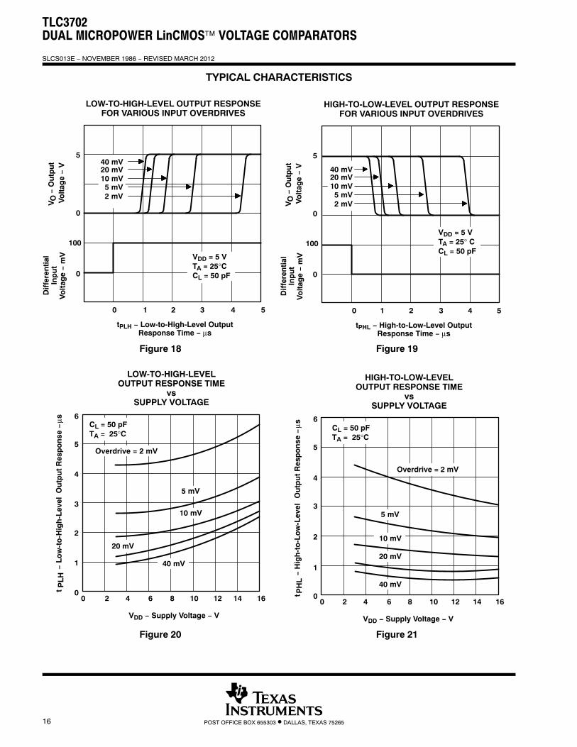
TYPICAL CHARACTERISTICS
Figure 18
0 1 2 3 4 5
VO
− O
utp
ut
Vo
ltag
e −
VIn
pu
tV
olt
age −
mV
Dif
fere
nti
al
LOW-TO-HIGH-LEVEL OUTPUT RESPONSEFOR VARIOUS INPUT OVERDRIVES
tPLH − Low-to-High-Level OutputResponse Time − μs
VDD = 5 VTA = 25°CCL = 50 pF
5
0
100
0
40 mV20 mV10 mV5 mV2 mV
Figure 19
40 mV20 mV10 mV5 mV2 mV
HIGH-TO-LOW-LEVEL OUTPUT RESPONSEFOR VARIOUS INPUT OVERDRIVES
tPHL − High-to-Low-Level OutputResponse Time − μs
VO
− O
utp
ut
Vo
ltag
e −
VIn
pu
tV
olt
age −
mV
Dif
fere
nti
al
5
0
100
0
0 1 2 3 4 5
VDD = 5 VTA = 25° CCL = 50 pF
Figure 20
LOW-TO-HIGH-LEVELOUTPUT RESPONSE TIME
vsSUPPLY VOLTAGE
Overdrive = 2 mV
5 mV
10 mV
20 mV
40 mV
6
5
4
3
2
1
00 2 4 6 8 10 12 14 16
VDD − Supply Voltage − V
CL = 50 pFTA = 25°C
tP
LH−
Lo
w-t
o-H
igh
-Lev
elO
utp
ut
Res
po
nse
−μs
Figure 21
HIGH-TO-LOW-LEVELOUTPUT RESPONSE TIME
vsSUPPLY VOLTAGE
6
5
4
3
2
1
00 2 4 6 8 10 12 14 16
5 mV
10 mV
20 mV
40 mV
CL = 50 pFTA = 25°C
VDD − Supply Voltage − V
t PH
L−
Hig
h-t
o-L
ow
-Lev
elO
utp
ut
Res
po
nse
−μs
Overdrive = 2 mV
TLC3702DUAL MICROPOWER LinCMOS™ VOLTAGE COMPARATORS
SLCS013E − NOVEMBER 1986 − REVISED MARCH 2012
17POST OFFICE BOX 655303 • DALLAS, TEXAS 75265
TYPICAL CHARACTERISTICS†
Figure 22
AVERAGE SUPPLY CURRENT(PER COMPARATOR)
vsFREQUENCY
10000
1000
100
10
V −
Su
pp
ly C
urr
ent −
μD
DA
0.01 0.1 1 10 100
f − Frequency − kHz
VDD = 16 V
5 V
4 V
10 V
3 V
TA = 25°CCL = 50 pF
Figure 23
SUPPLY CURRENTvs
SUPPLY VOLTAGE
VDD − Supply Voltage − V
40
35
30
25
20
15
10
5
00 1 2 3 4 5 6 7 8
Outputs LowNo Loads
V −
Su
pp
ly C
urr
ent −
μD
DA
TA = − 25°C
TA = − 125°C
TA = − 40°C
TA = − 55°C
TA = 85°C
SUPPLY CURRENTvs
FREE-AIR TEMPERATURE
30
25
20
15
10
5
0−75 −50 −25 0 25 50 75 100 125
TA − Free-Air Temperature − °C
I DD−
Su
pp
ly C
urr
ent −
μA
Outputs High
Outputs Low
VDD = 5 VNo Load
Figure 24
† Data at high and low temperatures are applicable only within the rated operating free-air temperature ranges of the various devices.
TLC3702DUAL MICROPOWER LinCMOS™ VOLTAGE COMPARATORS
SLCS013E − NOVEMBER 1986 − REVISED MARCH 2012
18 POST OFFICE BOX 655303 • DALLAS, TEXAS 75265
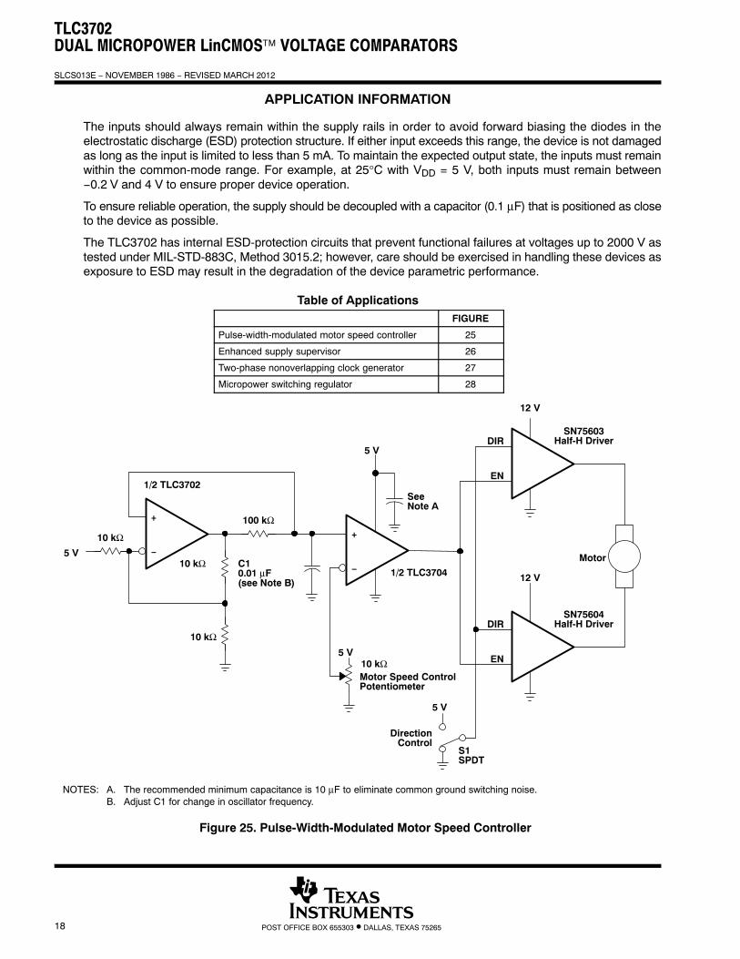
APPLICATION INFORMATION
The inputs should always remain within the supply rails in order to avoid forward biasing the diodes in theelectrostatic discharge (ESD) protection structure. If either input exceeds this range, the device is not damagedas long as the input is limited to less than 5 mA. To maintain the expected output state, the inputs must remainwithin the common-mode range. For example, at 25°C with VDD = 5 V, both inputs must remain between−0.2 V and 4 V to ensure proper device operation.
To ensure reliable operation, the supply should be decoupled with a capacitor (0.1 μF) that is positioned as closeto the device as possible.
The TLC3702 has internal ESD-protection circuits that prevent functional failures at voltages up to 2000 V astested under MIL-STD-883C, Method 3015.2; however, care should be exercised in handling these devices asexposure to ESD may result in the degradation of the device parametric performance.
Table of ApplicationsFIGURE
Pulse-width-modulated motor speed controller 25
Enhanced supply supervisor 26
Two-phase nonoverlapping clock generator 27
Micropower switching regulator 28
C10.01 μF(see Note B)
5 V
1/2 TLC3702
Motor Speed ControlPotentiometer
+
−
+
−10 kΩ
100 kΩ
10 kΩ
10 kΩ
SeeNote A
1/2 TLC3704
10 kΩ5 V
DIR
EN
SN75603Half-H Driver
12 V
Motor
DIR
EN
12 V
DirectionControl
S1SPDT
5 V
5 V
SN75604Half-H Driver
NOTES: A. The recommended minimum capacitance is 10 μF to eliminate common ground switching noise.B. Adjust C1 for change in oscillator frequency.
Figure 25. Pulse-Width-Modulated Motor Speed Controller
TLC3702DUAL MICROPOWER LinCMOS™ VOLTAGE COMPARATORS
SLCS013E − NOVEMBER 1986 − REVISED MARCH 2012
19POST OFFICE BOX 655303 • DALLAS, TEXAS 75265
APPLICATION INFORMATION
1/2 TLC3702
To μP InterruptEarly Power Fail
+
−
+
−
1 kΩ
3.3 kΩ
CT(see Note B)
1/2 TLC3702 10 kΩ
5 V
5 V
12-VSense
R2
R1V(UNREG)
(see Note A)
1 μF
12 V
RESIN
REF CT GND
RESET
SENSEVCC
To μPReset
Monitors 5 VDC RailMonitors 12 VDC RailEarly Power Fail Warning
TL7705A
2.5 V
NOTES: A. V(UNREG) � 2.5(R1 +R2)
R2B. The value of CT determines the time delay of reset.
Figure 26. Enhanced Supply Supervisor
TLC3702DUAL MICROPOWER LinCMOS™ VOLTAGE COMPARATORS
SLCS013E − NOVEMBER 1986 − REVISED MARCH 2012
20 POST OFFICE BOX 655303 • DALLAS, TEXAS 75265
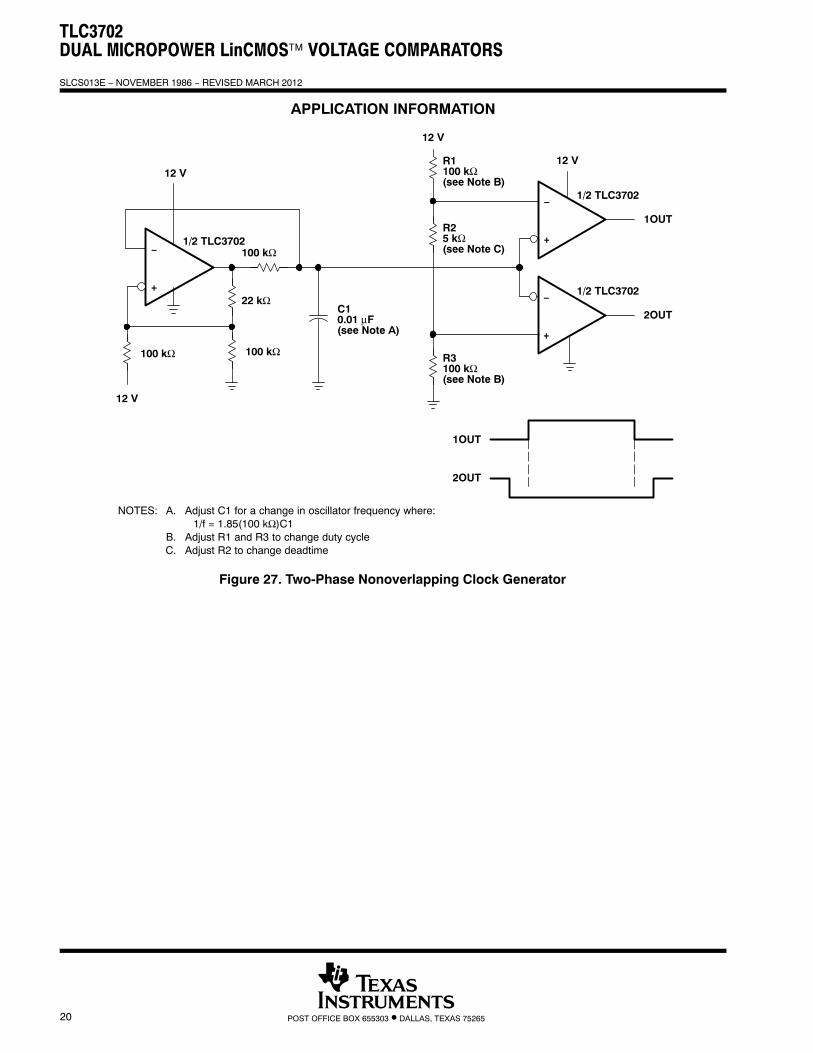
APPLICATION INFORMATION
−
+22 kΩ
C10.01 μF(see Note A)
1/2 TLC3702
R1100 kΩ(see Note B)
12 V
100 kΩ
1/2 TLC3702
2OUT
−
+
−
+
1/2 TLC3702
100 kΩ 100 kΩ
12 V
1OUT
12 V
R25 kΩ(see Note C)
R3100 kΩ(see Note B)
2OUT
1OUT
12 V
NOTES: A. Adjust C1 for a change in oscillator frequency where: 1/f = 1.85(100 kΩ)C1
B. Adjust R1 and R3 to change duty cycleC. Adjust R2 to change deadtime
Figure 27. Two-Phase Nonoverlapping Clock Generator
TLC3702DUAL MICROPOWER LinCMOS™ VOLTAGE COMPARATORS
SLCS013E − NOVEMBER 1986 − REVISED MARCH 2012
21POST OFFICE BOX 655303 • DALLAS, TEXAS 75265
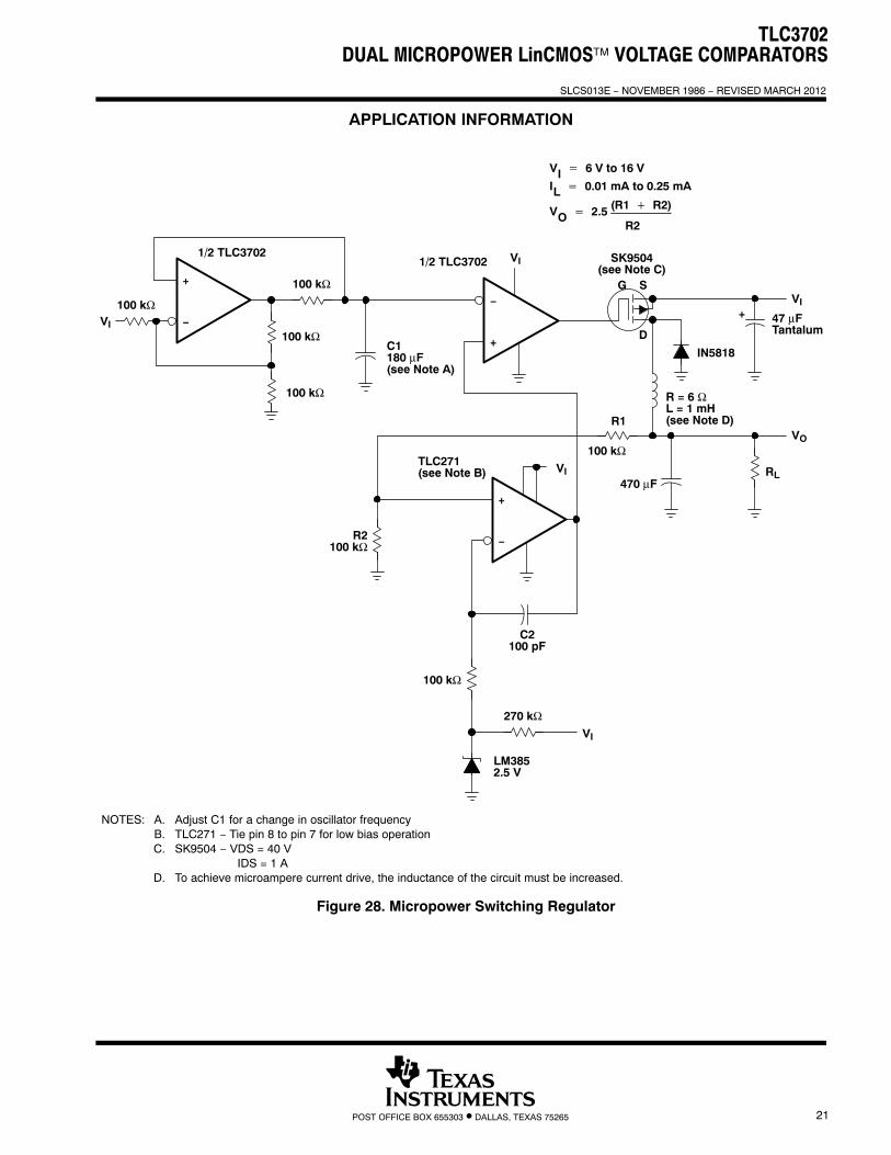
APPLICATION INFORMATION
+
−100 kΩ
C1180 μF(see Note A)
1/2 TLC3702
47 μFTantalum
100 kΩ
R2100 kΩ
100 kΩ
100 kΩVI
VI
−
+
1/2 TLC3702
VI
+
−
TLC271(see Note B)
270 kΩVI
100 kΩ
C2100 pF
100 kΩ
IN5818
R = 6 ΩL = 1 mH(see Note D)
RL470 μF
VI
VO
R1
G S
SK9504(see Note C)
VI � 6 V to 16 V
IL � 0.01 mA to 0.25 mA
VO � 2.5 (R1 � R2)
R2
LM3852.5 V
D
+
NOTES: A. Adjust C1 for a change in oscillator frequencyB. TLC271 − Tie pin 8 to pin 7 for low bias operationC. SK9504 − VDS = 40 V
IDS = 1 AD. To achieve microampere current drive, the inductance of the circuit must be increased.
Figure 28. Micropower Switching Regulator
PACKAGE OPTION ADDENDUM
www.ti.com 15-Apr-2017
Addendum-Page 1
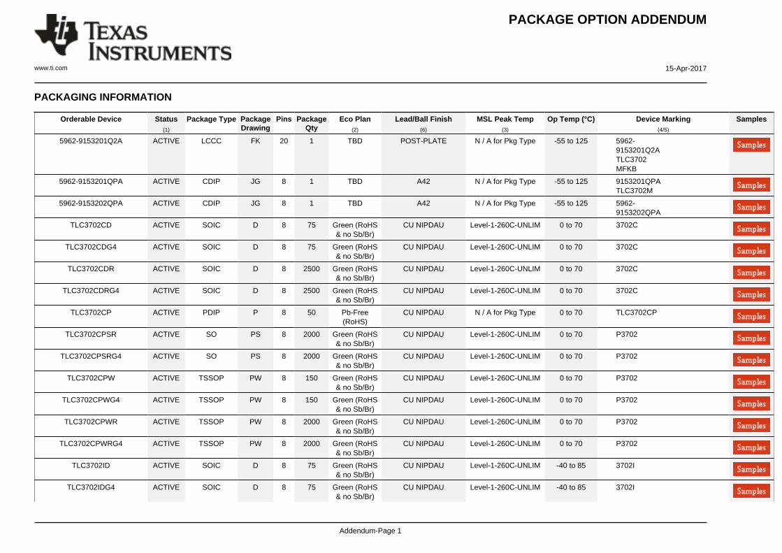
PACKAGING INFORMATION
Orderable Device Status(1)
Package Type PackageDrawing
Pins PackageQty
Eco Plan(2)
Lead/Ball Finish(6)
MSL Peak Temp(3)
Op Temp (°C) Device Marking(4/5)
Samples
5962-9153201Q2A ACTIVE LCCC FK 20 1 TBD POST-PLATE N / A for Pkg Type -55 to 125 5962-9153201Q2ATLC3702MFKB
5962-9153201QPA ACTIVE CDIP JG 8 1 TBD A42 N / A for Pkg Type -55 to 125 9153201QPATLC3702M
5962-9153202QPA ACTIVE CDIP JG 8 1 TBD A42 N / A for Pkg Type -55 to 125 5962-9153202QPA
TLC3702CD ACTIVE SOIC D 8 75 Green (RoHS& no Sb/Br)
CU NIPDAU Level-1-260C-UNLIM 0 to 70 3702C
TLC3702CDG4 ACTIVE SOIC D 8 75 Green (RoHS& no Sb/Br)
CU NIPDAU Level-1-260C-UNLIM 0 to 70 3702C
TLC3702CDR ACTIVE SOIC D 8 2500 Green (RoHS& no Sb/Br)
CU NIPDAU Level-1-260C-UNLIM 0 to 70 3702C
TLC3702CDRG4 ACTIVE SOIC D 8 2500 Green (RoHS& no Sb/Br)
CU NIPDAU Level-1-260C-UNLIM 0 to 70 3702C
TLC3702CP ACTIVE PDIP P 8 50 Pb-Free(RoHS)
CU NIPDAU N / A for Pkg Type 0 to 70 TLC3702CP
TLC3702CPSR ACTIVE SO PS 8 2000 Green (RoHS& no Sb/Br)
CU NIPDAU Level-1-260C-UNLIM 0 to 70 P3702
TLC3702CPSRG4 ACTIVE SO PS 8 2000 Green (RoHS& no Sb/Br)
CU NIPDAU Level-1-260C-UNLIM 0 to 70 P3702
TLC3702CPW ACTIVE TSSOP PW 8 150 Green (RoHS& no Sb/Br)
CU NIPDAU Level-1-260C-UNLIM 0 to 70 P3702
TLC3702CPWG4 ACTIVE TSSOP PW 8 150 Green (RoHS& no Sb/Br)
CU NIPDAU Level-1-260C-UNLIM 0 to 70 P3702
TLC3702CPWR ACTIVE TSSOP PW 8 2000 Green (RoHS& no Sb/Br)
CU NIPDAU Level-1-260C-UNLIM 0 to 70 P3702
TLC3702CPWRG4 ACTIVE TSSOP PW 8 2000 Green (RoHS& no Sb/Br)
CU NIPDAU Level-1-260C-UNLIM 0 to 70 P3702
TLC3702ID ACTIVE SOIC D 8 75 Green (RoHS& no Sb/Br)
CU NIPDAU Level-1-260C-UNLIM -40 to 85 3702I
TLC3702IDG4 ACTIVE SOIC D 8 75 Green (RoHS& no Sb/Br)
CU NIPDAU Level-1-260C-UNLIM -40 to 85 3702I
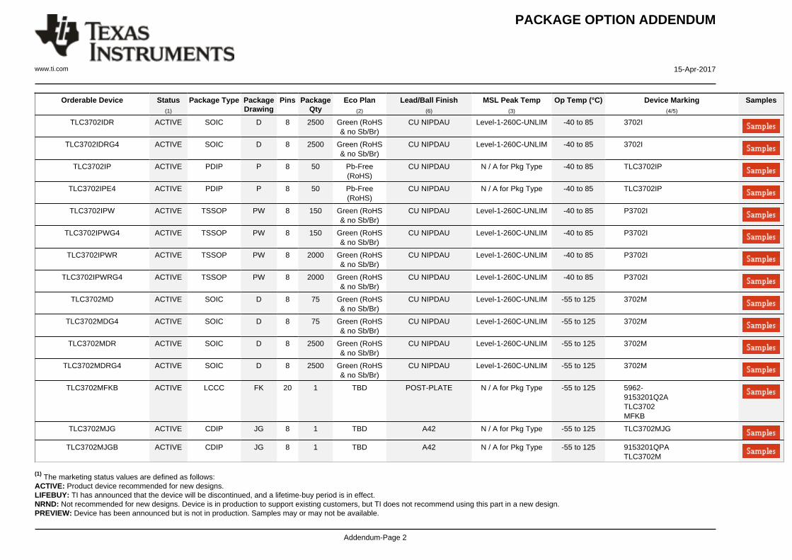
PACKAGE OPTION ADDENDUM
www.ti.com 15-Apr-2017
Addendum-Page 2
Orderable Device Status(1)
Package Type PackageDrawing
Pins PackageQty
Eco Plan(2)
Lead/Ball Finish(6)
MSL Peak Temp(3)
Op Temp (°C) Device Marking(4/5)
Samples
TLC3702IDR ACTIVE SOIC D 8 2500 Green (RoHS& no Sb/Br)
CU NIPDAU Level-1-260C-UNLIM -40 to 85 3702I
TLC3702IDRG4 ACTIVE SOIC D 8 2500 Green (RoHS& no Sb/Br)
CU NIPDAU Level-1-260C-UNLIM -40 to 85 3702I
TLC3702IP ACTIVE PDIP P 8 50 Pb-Free(RoHS)
CU NIPDAU N / A for Pkg Type -40 to 85 TLC3702IP
TLC3702IPE4 ACTIVE PDIP P 8 50 Pb-Free(RoHS)
CU NIPDAU N / A for Pkg Type -40 to 85 TLC3702IP
TLC3702IPW ACTIVE TSSOP PW 8 150 Green (RoHS& no Sb/Br)
CU NIPDAU Level-1-260C-UNLIM -40 to 85 P3702I
TLC3702IPWG4 ACTIVE TSSOP PW 8 150 Green (RoHS& no Sb/Br)
CU NIPDAU Level-1-260C-UNLIM -40 to 85 P3702I
TLC3702IPWR ACTIVE TSSOP PW 8 2000 Green (RoHS& no Sb/Br)
CU NIPDAU Level-1-260C-UNLIM -40 to 85 P3702I
TLC3702IPWRG4 ACTIVE TSSOP PW 8 2000 Green (RoHS& no Sb/Br)
CU NIPDAU Level-1-260C-UNLIM -40 to 85 P3702I
TLC3702MD ACTIVE SOIC D 8 75 Green (RoHS& no Sb/Br)
CU NIPDAU Level-1-260C-UNLIM -55 to 125 3702M
TLC3702MDG4 ACTIVE SOIC D 8 75 Green (RoHS& no Sb/Br)
CU NIPDAU Level-1-260C-UNLIM -55 to 125 3702M
TLC3702MDR ACTIVE SOIC D 8 2500 Green (RoHS& no Sb/Br)
CU NIPDAU Level-1-260C-UNLIM -55 to 125 3702M
TLC3702MDRG4 ACTIVE SOIC D 8 2500 Green (RoHS& no Sb/Br)
CU NIPDAU Level-1-260C-UNLIM -55 to 125 3702M
TLC3702MFKB ACTIVE LCCC FK 20 1 TBD POST-PLATE N / A for Pkg Type -55 to 125 5962-9153201Q2ATLC3702MFKB
TLC3702MJG ACTIVE CDIP JG 8 1 TBD A42 N / A for Pkg Type -55 to 125 TLC3702MJG
TLC3702MJGB ACTIVE CDIP JG 8 1 TBD A42 N / A for Pkg Type -55 to 125 9153201QPATLC3702M
(1) The marketing status values are defined as follows:ACTIVE: Product device recommended for new designs.LIFEBUY: TI has announced that the device will be discontinued, and a lifetime-buy period is in effect.NRND: Not recommended for new designs. Device is in production to support existing customers, but TI does not recommend using this part in a new design.PREVIEW: Device has been announced but is not in production. Samples may or may not be available.
PACKAGE OPTION ADDENDUM
www.ti.com 15-Apr-2017
Addendum-Page 3
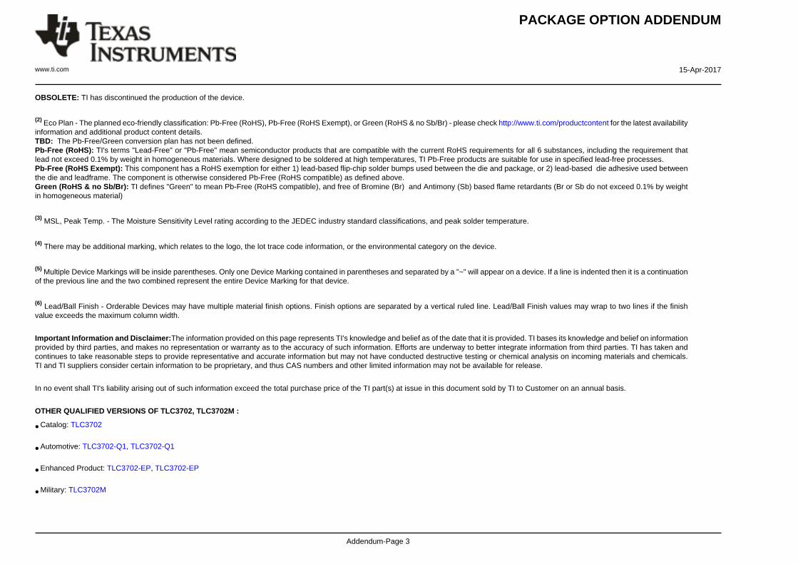
OBSOLETE: TI has discontinued the production of the device.
(2) Eco Plan - The planned eco-friendly classification: Pb-Free (RoHS), Pb-Free (RoHS Exempt), or Green (RoHS & no Sb/Br) - please check http://www.ti.com/productcontent for the latest availabilityinformation and additional product content details.TBD: The Pb-Free/Green conversion plan has not been defined.Pb-Free (RoHS): TI's terms "Lead-Free" or "Pb-Free" mean semiconductor products that are compatible with the current RoHS requirements for all 6 substances, including the requirement thatlead not exceed 0.1% by weight in homogeneous materials. Where designed to be soldered at high temperatures, TI Pb-Free products are suitable for use in specified lead-free processes.Pb-Free (RoHS Exempt): This component has a RoHS exemption for either 1) lead-based flip-chip solder bumps used between the die and package, or 2) lead-based die adhesive used betweenthe die and leadframe. The component is otherwise considered Pb-Free (RoHS compatible) as defined above.Green (RoHS & no Sb/Br): TI defines "Green" to mean Pb-Free (RoHS compatible), and free of Bromine (Br) and Antimony (Sb) based flame retardants (Br or Sb do not exceed 0.1% by weightin homogeneous material)
(3) MSL, Peak Temp. - The Moisture Sensitivity Level rating according to the JEDEC industry standard classifications, and peak solder temperature.
(4) There may be additional marking, which relates to the logo, the lot trace code information, or the environmental category on the device.
(5) Multiple Device Markings will be inside parentheses. Only one Device Marking contained in parentheses and separated by a "~" will appear on a device. If a line is indented then it is a continuationof the previous line and the two combined represent the entire Device Marking for that device.
(6) Lead/Ball Finish - Orderable Devices may have multiple material finish options. Finish options are separated by a vertical ruled line. Lead/Ball Finish values may wrap to two lines if the finishvalue exceeds the maximum column width.
Important Information and Disclaimer:The information provided on this page represents TI's knowledge and belief as of the date that it is provided. TI bases its knowledge and belief on informationprovided by third parties, and makes no representation or warranty as to the accuracy of such information. Efforts are underway to better integrate information from third parties. TI has taken andcontinues to take reasonable steps to provide representative and accurate information but may not have conducted destructive testing or chemical analysis on incoming materials and chemicals.TI and TI suppliers consider certain information to be proprietary, and thus CAS numbers and other limited information may not be available for release.
In no event shall TI's liability arising out of such information exceed the total purchase price of the TI part(s) at issue in this document sold by TI to Customer on an annual basis.
OTHER QUALIFIED VERSIONS OF TLC3702, TLC3702M :
• Catalog: TLC3702
• Automotive: TLC3702-Q1, TLC3702-Q1
• Enhanced Product: TLC3702-EP, TLC3702-EP
• Military: TLC3702M
PACKAGE OPTION ADDENDUM
www.ti.com 15-Apr-2017
Addendum-Page 4
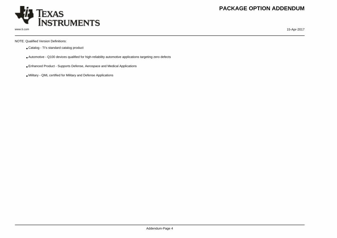
NOTE: Qualified Version Definitions:
• Catalog - TI's standard catalog product
• Automotive - Q100 devices qualified for high-reliability automotive applications targeting zero defects
• Enhanced Product - Supports Defense, Aerospace and Medical Applications
• Military - QML certified for Military and Defense Applications
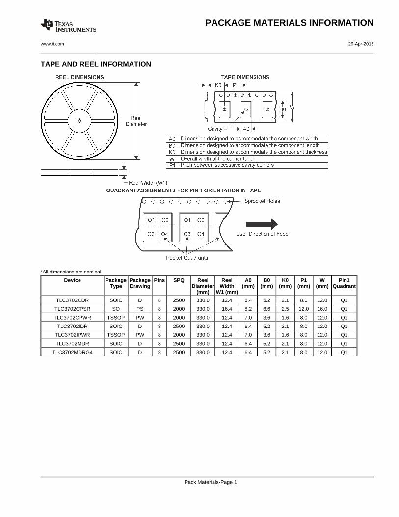
TAPE AND REEL INFORMATION
*All dimensions are nominal
Device PackageType
PackageDrawing
Pins SPQ ReelDiameter
(mm)
ReelWidth
W1 (mm)
A0(mm)
B0(mm)
K0(mm)
P1(mm)
W(mm)
Pin1Quadrant
TLC3702CDR SOIC D 8 2500 330.0 12.4 6.4 5.2 2.1 8.0 12.0 Q1
TLC3702CPSR SO PS 8 2000 330.0 16.4 8.2 6.6 2.5 12.0 16.0 Q1
TLC3702CPWR TSSOP PW 8 2000 330.0 12.4 7.0 3.6 1.6 8.0 12.0 Q1
TLC3702IDR SOIC D 8 2500 330.0 12.4 6.4 5.2 2.1 8.0 12.0 Q1
TLC3702IPWR TSSOP PW 8 2000 330.0 12.4 7.0 3.6 1.6 8.0 12.0 Q1
TLC3702MDR SOIC D 8 2500 330.0 12.4 6.4 5.2 2.1 8.0 12.0 Q1
TLC3702MDRG4 SOIC D 8 2500 330.0 12.4 6.4 5.2 2.1 8.0 12.0 Q1
PACKAGE MATERIALS INFORMATION
www.ti.com 29-Apr-2016
Pack Materials-Page 1
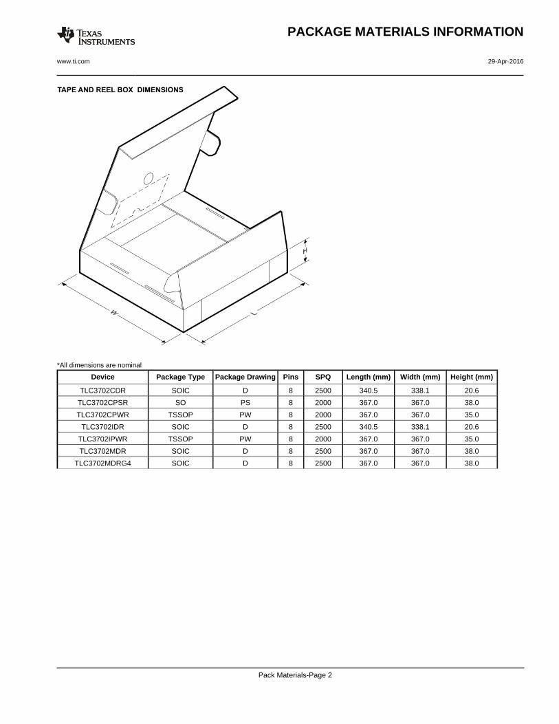
*All dimensions are nominal
Device Package Type Package Drawing Pins SPQ Length (mm) Width (mm) Height (mm)
TLC3702CDR SOIC D 8 2500 340.5 338.1 20.6
TLC3702CPSR SO PS 8 2000 367.0 367.0 38.0
TLC3702CPWR TSSOP PW 8 2000 367.0 367.0 35.0
TLC3702IDR SOIC D 8 2500 340.5 338.1 20.6
TLC3702IPWR TSSOP PW 8 2000 367.0 367.0 35.0
TLC3702MDR SOIC D 8 2500 367.0 367.0 38.0
TLC3702MDRG4 SOIC D 8 2500 367.0 367.0 38.0
PACKAGE MATERIALS INFORMATION
www.ti.com 29-Apr-2016
Pack Materials-Page 2
MECHANICAL DATA
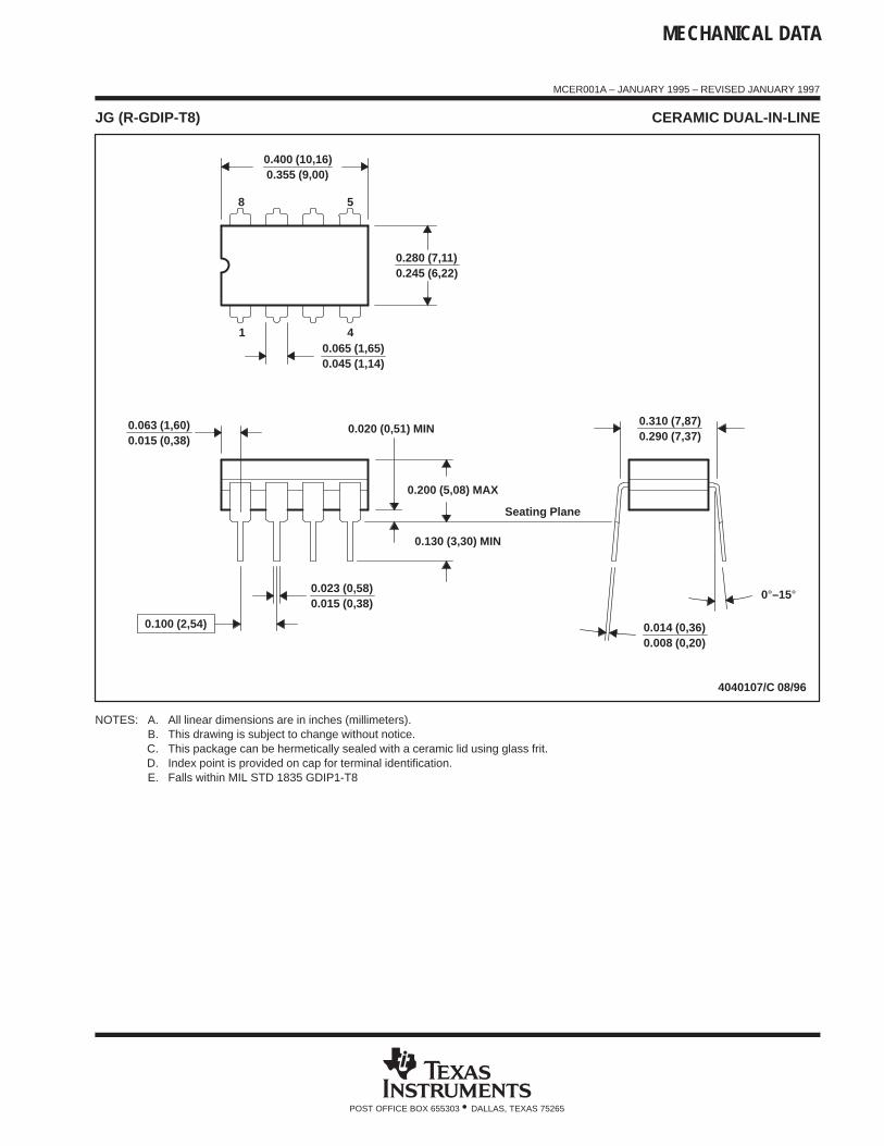
MCER001A – JANUARY 1995 – REVISED JANUARY 1997
POST OFFICE BOX 655303 • DALLAS, TEXAS 75265
JG (R-GDIP-T8) CERAMIC DUAL-IN-LINE
0.310 (7,87)0.290 (7,37)
0.014 (0,36)0.008 (0,20)
Seating Plane
4040107/C 08/96
5
40.065 (1,65)0.045 (1,14)
8
1
0.020 (0,51) MIN
0.400 (10,16)0.355 (9,00)
0.015 (0,38)0.023 (0,58)
0.063 (1,60)0.015 (0,38)
0.200 (5,08) MAX
0.130 (3,30) MIN
0.245 (6,22)0.280 (7,11)
0.100 (2,54)
0°–15°
NOTES: A. All linear dimensions are in inches (millimeters).B. This drawing is subject to change without notice.C. This package can be hermetically sealed with a ceramic lid using glass frit.D. Index point is provided on cap for terminal identification.E. Falls within MIL STD 1835 GDIP1-T8
www.ti.com
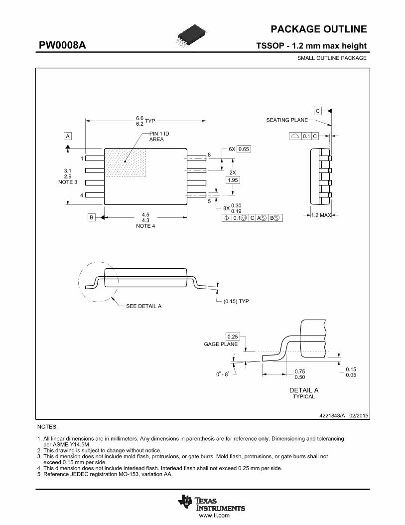
PACKAGE OUTLINE
C
TYP6.66.2
1.2 MAX
6X 0.65
8X 0.300.19
2X1.95
0.150.05
(0.15) TYP
0 - 8
0.25GAGE PLANE
0.750.50
A
NOTE 3
3.12.9
BNOTE 4
4.54.3
4221848/A 02/2015
TSSOP - 1.2 mm max heightPW0008ASMALL OUTLINE PACKAGE
NOTES: 1. All linear dimensions are in millimeters. Any dimensions in parenthesis are for reference only. Dimensioning and tolerancing per ASME Y14.5M. 2. This drawing is subject to change without notice. 3. This dimension does not include mold flash, protrusions, or gate burrs. Mold flash, protrusions, or gate burrs shall not exceed 0.15 mm per side. 4. This dimension does not include interlead flash. Interlead flash shall not exceed 0.25 mm per side.5. Reference JEDEC registration MO-153, variation AA.
18
0.1 C A B
54
PIN 1 IDAREA
SEATING PLANE
0.1 C
SEE DETAIL A
DETAIL ATYPICAL
SCALE 2.800
www.ti.com
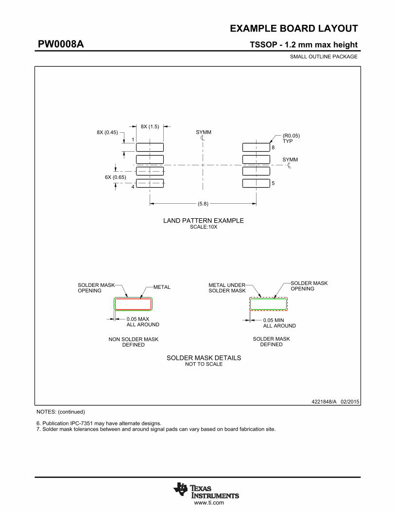
EXAMPLE BOARD LAYOUT
(5.8)
0.05 MAXALL AROUND
0.05 MINALL AROUND
8X (1.5)8X (0.45)
6X (0.65)
(R )TYP
0.05
4221848/A 02/2015
TSSOP - 1.2 mm max heightPW0008ASMALL OUTLINE PACKAGE
SYMM
SYMM
LAND PATTERN EXAMPLESCALE:10X
1
45
8
NOTES: (continued) 6. Publication IPC-7351 may have alternate designs. 7. Solder mask tolerances between and around signal pads can vary based on board fabrication site.
METALSOLDER MASKOPENING
NON SOLDER MASKDEFINED
SOLDER MASK DETAILSNOT TO SCALE
SOLDER MASKOPENING
METAL UNDERSOLDER MASK
SOLDER MASKDEFINED
www.ti.com
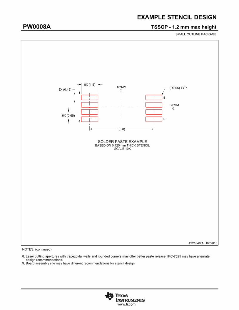
EXAMPLE STENCIL DESIGN
(5.8)
6X (0.65)
8X (0.45)8X (1.5)
(R ) TYP0.05
4221848/A 02/2015
TSSOP - 1.2 mm max heightPW0008ASMALL OUTLINE PACKAGE
NOTES: (continued) 8. Laser cutting apertures with trapezoidal walls and rounded corners may offer better paste release. IPC-7525 may have alternate design recommendations. 9. Board assembly site may have different recommendations for stencil design.
SYMM
SYMM
1
45
8
SOLDER PASTE EXAMPLEBASED ON 0.125 mm THICK STENCIL
SCALE:10X
IMPORTANT NOTICE
Texas Instruments Incorporated (TI) reserves the right to make corrections, enhancements, improvements and other changes to itssemiconductor products and services per JESD46, latest issue, and to discontinue any product or service per JESD48, latest issue. Buyersshould obtain the latest relevant information before placing orders and should verify that such information is current and complete.TI’s published terms of sale for semiconductor products (http://www.ti.com/sc/docs/stdterms.htm) apply to the sale of packaged integratedcircuit products that TI has qualified and released to market. Additional terms may apply to the use or sale of other types of TI products andservices.Reproduction of significant portions of TI information in TI data sheets is permissible only if reproduction is without alteration and isaccompanied by all associated warranties, conditions, limitations, and notices. TI is not responsible or liable for such reproduceddocumentation. Information of third parties may be subject to additional restrictions. Resale of TI products or services with statementsdifferent from or beyond the parameters stated by TI for that product or service voids all express and any implied warranties for theassociated TI product or service and is an unfair and deceptive business practice. TI is not responsible or liable for any such statements.Buyers and others who are developing systems that incorporate TI products (collectively, “Designers”) understand and agree that Designersremain responsible for using their independent analysis, evaluation and judgment in designing their applications and that Designers havefull and exclusive responsibility to assure the safety of Designers' applications and compliance of their applications (and of all TI productsused in or for Designers’ applications) with all applicable regulations, laws and other applicable requirements. Designer represents that, withrespect to their applications, Designer has all the necessary expertise to create and implement safeguards that (1) anticipate dangerousconsequences of failures, (2) monitor failures and their consequences, and (3) lessen the likelihood of failures that might cause harm andtake appropriate actions. Designer agrees that prior to using or distributing any applications that include TI products, Designer willthoroughly test such applications and the functionality of such TI products as used in such applications.TI’s provision of technical, application or other design advice, quality characterization, reliability data or other services or information,including, but not limited to, reference designs and materials relating to evaluation modules, (collectively, “TI Resources”) are intended toassist designers who are developing applications that incorporate TI products; by downloading, accessing or using TI Resources in anyway, Designer (individually or, if Designer is acting on behalf of a company, Designer’s company) agrees to use any particular TI Resourcesolely for this purpose and subject to the terms of this Notice.TI’s provision of TI Resources does not expand or otherwise alter TI’s applicable published warranties or warranty disclaimers for TIproducts, and no additional obligations or liabilities arise from TI providing such TI Resources. TI reserves the right to make corrections,enhancements, improvements and other changes to its TI Resources. TI has not conducted any testing other than that specificallydescribed in the published documentation for a particular TI Resource.Designer is authorized to use, copy and modify any individual TI Resource only in connection with the development of applications thatinclude the TI product(s) identified in such TI Resource. NO OTHER LICENSE, EXPRESS OR IMPLIED, BY ESTOPPEL OR OTHERWISETO ANY OTHER TI INTELLECTUAL PROPERTY RIGHT, AND NO LICENSE TO ANY TECHNOLOGY OR INTELLECTUAL PROPERTYRIGHT OF TI OR ANY THIRD PARTY IS GRANTED HEREIN, including but not limited to any patent right, copyright, mask work right, orother intellectual property right relating to any combination, machine, or process in which TI products or services are used. Informationregarding or referencing third-party products or services does not constitute a license to use such products or services, or a warranty orendorsement thereof. Use of TI Resources may require a license from a third party under the patents or other intellectual property of thethird party, or a license from TI under the patents or other intellectual property of TI.TI RESOURCES ARE PROVIDED “AS IS” AND WITH ALL FAULTS. TI DISCLAIMS ALL OTHER WARRANTIES ORREPRESENTATIONS, EXPRESS OR IMPLIED, REGARDING RESOURCES OR USE THEREOF, INCLUDING BUT NOT LIMITED TOACCURACY OR COMPLETENESS, TITLE, ANY EPIDEMIC FAILURE WARRANTY AND ANY IMPLIED WARRANTIES OFMERCHANTABILITY, FITNESS FOR A PARTICULAR PURPOSE, AND NON-INFRINGEMENT OF ANY THIRD PARTY INTELLECTUALPROPERTY RIGHTS. TI SHALL NOT BE LIABLE FOR AND SHALL NOT DEFEND OR INDEMNIFY DESIGNER AGAINST ANY CLAIM,INCLUDING BUT NOT LIMITED TO ANY INFRINGEMENT CLAIM THAT RELATES TO OR IS BASED ON ANY COMBINATION OFPRODUCTS EVEN IF DESCRIBED IN TI RESOURCES OR OTHERWISE. IN NO EVENT SHALL TI BE LIABLE FOR ANY ACTUAL,DIRECT, SPECIAL, COLLATERAL, INDIRECT, PUNITIVE, INCIDENTAL, CONSEQUENTIAL OR EXEMPLARY DAMAGES INCONNECTION WITH OR ARISING OUT OF TI RESOURCES OR USE THEREOF, AND REGARDLESS OF WHETHER TI HAS BEENADVISED OF THE POSSIBILITY OF SUCH DAMAGES.Unless TI has explicitly designated an individual product as meeting the requirements of a particular industry standard (e.g., ISO/TS 16949and ISO 26262), TI is not responsible for any failure to meet such industry standard requirements.Where TI specifically promotes products as facilitating functional safety or as compliant with industry functional safety standards, suchproducts are intended to help enable customers to design and create their own applications that meet applicable functional safety standardsand requirements. Using products in an application does not by itself establish any safety features in the application. Designers mustensure compliance with safety-related requirements and standards applicable to their applications. Designer may not use any TI products inlife-critical medical equipment unless authorized officers of the parties have executed a special contract specifically governing such use.Life-critical medical equipment is medical equipment where failure of such equipment would cause serious bodily injury or death (e.g., lifesupport, pacemakers, defibrillators, heart pumps, neurostimulators, and implantables). Such equipment includes, without limitation, allmedical devices identified by the U.S. Food and Drug Administration as Class III devices and equivalent classifications outside the U.S.TI may expressly designate certain products as completing a particular qualification (e.g., Q100, Military Grade, or Enhanced Product).Designers agree that it has the necessary expertise to select the product with the appropriate qualification designation for their applicationsand that proper product selection is at Designers’ own risk. Designers are solely responsible for compliance with all legal and regulatoryrequirements in connection with such selection.Designer will fully indemnify TI and its representatives against any damages, costs, losses, and/or liabilities arising out of Designer’s non-compliance with the terms and provisions of this Notice.
Mailing Address: Texas Instruments, Post Office Box 655303, Dallas, Texas 75265Copyright © 2017, Texas Instruments Incorporated