DSP Lock-In Amplifier model SR830 - Electrical and Computer
174
DSP Lock-In Amplifier model SR830 1290 D Reamwood Avenue Sunnyvale, CA 94089 USA Phone: (408) 744-9040 • Fax: (408) 744-9049 www.thinkSRS.com •e-mail: [email protected] Copyright © 1999 All Rights Reserved Revision 1.5 • 11/99 Stanford Research Systems
Transcript of DSP Lock-In Amplifier model SR830 - Electrical and Computer
DSP Lock-In Amplifier
model SR830
1290 D Reamwood AvenueSunnyvale, CA 94089 USA
Phone: (408) 744-9040 • Fax: (408) 744-9049www.thinkSRS.com •e-mail: [email protected]
Copyright© 1999All Rights Reserved
Revision 1.5 • 11/99
Stanford Research Systems
GENERAL INFORMATIONSafety and Preparation for Use 1-3Specifications 1-5Abridged Command List 1-7
GETTING STARTEDYour First Measurements 2-1The Basic Lock-in 2-3X, Y, R and θ 2-7Outputs, Offsets and Expands 2-9Storing and Recalling Setups 2-13Aux Outputs and Inputs 2-15
SR830 BASICSWhat is a Lock-in Amplifier? 3-1What Does a Lock-in Measure? 3-3The SR830 Functional Diagram 3-5Reference Channel 3-7Phase Sensitive Detectors 3-9Time Constants and DC Gain 3-11DC Outputs and Scaling 3-13Dynamic Reserve 3-15Signal Input Amplifier and Filters 3-17Input Connections 3-19Intrinsic (Random) Noise Sources 3-21External Noise Sources 3-23Noise Measurements 3-25
OPERATIONPower On/Off and Power On Tests 4-1Reset 4-1[Keys] 4-1Spin Knob 4-1Front Panel BNC Connectors 4-2Key Click On/Off 4-2Front Panel Display Test 4-2Display Off Operation 4-2Keypad Test 4-3Standard Settings 4-4
FRONT PANEL Signal Input and Filters 4-5Sensitivity, Reserve, Time Constants 4-7CH1 Display and Output 4-12CH2 Display and Output 4-15Reference 4-18Auto Functions 4-21Setup 4-23Interface 4-24Warning Messages 4-26
REAR PANEL Power Entry Module 4-27IEEE-488 Connector 4-27RS232 Connector 4-27Aux Inputs (A/D Inputs) 4-27Aux Outputs (D/A Outputs) 4-27X and Y Outputs 4-27Signal Monitor Output 4-28Trigger Input 4-28TTL Sync Output 4-28Preamp Connector 4-28Using SRS Preamps 4-29
PROGRAMMINGGPIB Communications 5-1RS232 Communications 5-1Status Indicators and Queues 5-1Command Syntax 5-1Interface Ready and Status 5-2GET (Group Execute Trigger) 5-2
DETAILED COMMAND LIST 5-3Reference and Phase 5-4Input and Filter 5-5Gain and Time Constant 5-6Display and Output 5-8Aux Input and Output 5-9Setup 5-10Auto Functions 5-11Data Storage 5-12Data Transfer 5-15Interface 5-19Status Reporting 5-20
STATUS BYTE DEFINITIONSSerial Poll Status Byte 5-21Service Requests 5-22Standard Event Status Byte 5-22LIA Status Byte 5-23Error Status Byte 5-23
PROGRAM EXAMPLES Microsoft C, Nationall Instr GPIB 5-25
USING SR530 PROGRAMS 5-31
TABLE OF CONTENTS
Table of Contents
TESTINGIntroduction 6-1Preset 6-1Serial Number 6-1Firmware Revision 6-1Test Record 6-1If A Test Fails 6-1Necessary Equipment 6-1Front Panel Display Test 6-2Keypad Test 6-2
PERFORMANCE TESTSSelf Tests 6-3DC Offset 6-5Common Mode Rejection 6-7Amplitude Accuracy and Flatness 6-9Amplitude Linearity 6-11Frequency Accuracy 6-13Phase Accuracy 6-15Sine Output Amplitude 6-17DC Outputs and Inputs 6-19Input Noise 6-21Performance Test Record 6-23
CIRCUITRYCircuit Boards 7-1CPU and Power Supply Board 7-3DSP Logic Board 7-5Analog Input Board 7-7
PARTS LISTSDSP Logic Board 7-9Analog Input Board 7-15CPU and Power Supply Board 7-21Front Panel Display Boards 7-24Miscellaneous 7-30
SCHEMATIC DIAGRAMSCPU and Power Supply BoardDisplay BoardKeypad BoardDSP Logic BoardAnalog Input Board
SAFETY AND PREPARATION FOR USE
CAUTION
This instrument may be damaged if operatedwith the LINE VOLTAGE SELECTOR set for thewrong AC line voltage or if the wrong fuse isinstalled.
LINE VOLTAGE SELECTION
The SR830 operates from a 100V, 120V, 220V, or240V nominal AC power source having a line fre-quency of 50 or 60 Hz. Before connecting the pow-er cord to a power source, verify that the LINEVOLTAGE SELECTOR card, located in the rearpanel fuse holder, is set so that the correct AC in-put voltage value is visible.
Conversion to other AC input voltages requires achange in the fuse holder voltage card positionand fuse value. Disconnect the power cord, openthe fuse holder cover door and rotate the fuse-pulllever to remove the fuse. Remove the small print-ed circuit board and select the operating voltageby orienting the printed circuit board so that thedesired voltage is visible when pushed firmly intoits slot. Rotate the fuse-pull lever back into its nor-mal position and insert the correct fuse into thefuse holder.
LINE FUSE
Verify that the correct line fuse is installed beforeconnecting the line cord. For 100V/120V, use a 1Amp fuse and for 220V/240V, use a 1/2 Amp fuse.
LINE CORD
The SR830 has a detachable, three-wire powercord for connection to the power source and to aprotective ground. The exposed metal parts of theinstrument are connected to the outlet ground toprotect against electrical shock. Always use anoutlet which has a properly connected protectiveground.
SERVICE
Do not attempt to service or adjust this instrumentunless another person, capable of providing firstaid or resuscitation, is present.
Do not install substitute parts or perform any unau-thorized modifications to this instrument. Contactthe factory for instructions on how to return the in-strument for authorized service and adjustment.
WARNING
Dangerous voltages, capable of causing injury or death, are present inthis instrument. Use extreme caution whenever the instrument coversare removed. Do not remove the covers while the unit is plugged into alive outlet.
1-3

1-4
SR830 DSP LOCK-IN AMPLIFIER
1-5
SPECIFICATIONSSIGNAL CHANNEL
Voltage Inputs Single-ended (A) or differential (A-B).Current Input 106 or 108 Volts/Amp.Full Scale Sensitivity 2 nV to 1 V in a 1-2-5-10 sequence (expand off).Input Impedance Voltage: 10 MΩ+25 pF, AC or DC coupled.
Current: 1 kΩ to virtual ground.Gain Accuracy ±1% from 20°C to 30°C (notch filters off).Input Noise 6 nV/√Hz at 1 kHz (typical).Signal Filters 60 (50) Hz and 120(100) Hz notch filters (Q=4).CMRR 90 dB at 100 Hz (DC Coupled).Dynamic Reserve Greater than 100 dB (with no signal filters).Harmonic Distortion -80 dB.
REFERENCE CHANNELFrequency Range 1 mHz to 102 kHzReference Input TTL (rising or falling edge) or Sine.
Sine input is1 MΩ, AC coupled (>1 Hz). 400 mV pk-pk minimum signal.Phase Resolution 0.01°Absolute Phase Error <1°Relative Phase Error <0.01°Orthogonality 90° ± 0.001°Phase Noise External synthesized reference: 0.005° rms at 1 kHz, 100 ms, 12 dB/oct.
Internal reference: crystal synthesized, <0.0001° rms at 1 kHz.Phase Drift <0.01°/°C below 10 kHz
<0.1°/°C to 100 kHzHarmonic Detect Detect at Nxf where N<19999 and Nxf<102 kHz.Acquisition Time (2 cycles + 5 ms) or 40 ms, whichever is greater.
DEMODULATORZero Stability Digital displays have no zero drift on all dynamic reserves.
Analog outputs: <5 ppm/°C for all dynamic reserves.Time Constants 10 µs to 30 s (reference > 200 Hz). 6, 12, 18, 24 dB/oct rolloff.
up to 30000 s (reference < 200 Hz). 6, 12, 18, 24 dB/oct rolloff.Synchronous filtering available below 200 Hz.
Harmonic Rejection -80 dB
INTERNAL OSCILLATORFrequency 1 mHz to 102 kHz.Frequency Accuracy 25 ppm + 30 µHzFrequency Resolution 4 1/2 digits or 0.1 mHz, whichever is greater.Distortion f<10 kHz, below -80 dBc. f>10 kHz, below -70 dBc.1 Vrms amplitude.Output Impedance 50 ΩAmplitude 4 mVrms to 5 Vrms (into a high impedance load) with 2 mV resolution.
(2 mVrms to 2.5 Vrms into 50Ω load).Amplitude Accuracy 1%Amplitude Stability 50 ppm/°COutputs Sine output on front panel. TTL sync output on rear panel.
When using an external reference, both outputs are phase locked to theexternal reference.
SR830 DSP Lock-In Amplifier
1-6
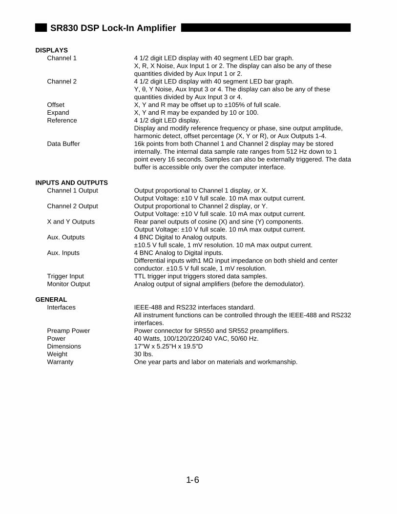
DISPLAYSChannel 1 4 1/2 digit LED display with 40 segment LED bar graph.
X, R, X Noise, Aux Input 1 or 2. The display can also be any of thesequantities divided by Aux Input 1 or 2.
Channel 2 4 1/2 digit LED display with 40 segment LED bar graph.Y, θ, Y Noise, Aux Input 3 or 4. The display can also be any of thesequantities divided by Aux Input 3 or 4.
Offset X, Y and R may be offset up to ±105% of full scale.Expand X, Y and R may be expanded by 10 or 100.Reference 4 1/2 digit LED display.
Display and modify reference frequency or phase, sine output amplitude,harmonic detect, offset percentage (X, Y or R), or Aux Outputs 1-4.
Data Buffer 16k points from both Channel 1 and Channel 2 display may be storedinternally. The internal data sample rate ranges from 512 Hz down to 1point every 16 seconds. Samples can also be externally triggered. The databuffer is accessible only over the computer interface.
INPUTS AND OUTPUTSChannel 1 Output Output proportional to Channel 1 display, or X.
Output Voltage: ±10 V full scale. 10 mA max output current.Channel 2 Output Output proportional to Channel 2 display, or Y.
Output Voltage: ±10 V full scale. 10 mA max output current.X and Y Outputs Rear panel outputs of cosine (X) and sine (Y) components.
Output Voltage: ±10 V full scale. 10 mA max output current.Aux. Outputs 4 BNC Digital to Analog outputs.
±10.5 V full scale, 1 mV resolution. 10 mA max output current.Aux. Inputs 4 BNC Analog to Digital inputs.
Differential inputs with1 MΩ input impedance on both shield and centerconductor. ±10.5 V full scale, 1 mV resolution.
Trigger Input TTL trigger input triggers stored data samples.Monitor Output Analog output of signal amplifiers (before the demodulator).
GENERALInterfaces IEEE-488 and RS232 interfaces standard.
All instrument functions can be controlled through the IEEE-488 and RS232interfaces.
Preamp Power Power connector for SR550 and SR552 preamplifiers.Power 40 Watts, 100/120/220/240 VAC, 50/60 Hz.Dimensions 17"W x 5.25"H x 19.5"DWeight 30 lbs.Warranty One year parts and labor on materials and workmanship.
SR830 DSP Lock-In Amplifier
1-7
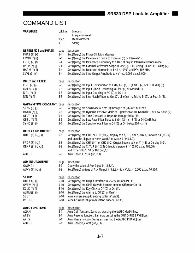
COMMAND LISTVARIABLES i,j,k,l,m Integers
f Frequency (real)x,y,z Real Numberss String
REFERENCE and PHASE page descriptionPHAS (?) x 5-4 Set (Query) the Phase Shift to x degrees.FMOD (?) i 5-4 Set (Query) the Reference Source to External (0) or Internal (1).FREQ (?) f 5-4 Set (Query) the Reference Frequency to f Hz.Set only in Internal reference mode.RSLP (?) i 5-4 Set (Query) the External Reference Slope to Sine(0), TTL Rising (1), or TTL Falling (2).HARM (?) i 5-4 Set (Query) the Detection Harmonic to 1 ≤ i ≤ 19999 and i•f ≤ 102 kHz.SLVL (?) x 5-4 Set (Query) the Sine Output Amplitude to x Vrms. 0.004 ≤ x ≤5.000.
INPUT and FILTER page descriptionISRC (?) i 5-5 Set (Query) the Input Configuration to A (0), A-B (1) , I (1 MΩ) (2) or I (100 MΩ) (3).IGND (?) i 5-5 Set (Query) the Input Shield Grounding to Float (0) or Ground (1).ICPL (?) i 5-5 Set (Query) the Input Coupling to AC (0) or DC (1).ILIN (?) i 5-5 Set (Query) the Line Notch Filters to Out (0), Line In (1) , 2xLine In (2), or Both In (3).
GAIN and TIME CONSTANT page descriptionSENS (?) i 5-6 Set (Query) the Sensitivity to 2 nV (0) through 1 V (26) rms full scale.RMOD (?) i 5-6 Set (Query) the Dynamic Reserve Mode to HighReserve (0), Normal (1), or Low Noise (2).OFLT (?) i 5-6 Set (Query) the Time Constant to 10 µs (0) through 30 ks (19).OFSL (?) i 5-6 Set (Query) the Low Pass Filter Slope to 6 (0), 12 (1), 18 (2) or 24 (3) dB/oct.SYNC (?) i 5-7 Set (Query) the Synchronous Filter to Off (0) or On below 200 Hz (1).
DISPLAY and OUTPUT page descriptionDDEF (?) i , j, k 5-8 Set (Query) the CH1 or CH2 (i=1,2) display to XY, Rθ, XnYn, Aux 1,3 or Aux 2,4 (j=0..4)
and ratio the display to None, Aux1,3 or Aux 2,4 (k=0,1,2).FPOP (?) i , j 5-8 Set (Query) the CH1 (i=1) or CH2 (i=2) Output Source to X or Y (j=1) or Display (j=0).OEXP (?) i , x, j 5-8 Set (Query) the X, Y, R (i=1,2,3) Offset to x percent ( -105.00 ≤ x ≤ 105.00)
and Expand to 1, 10 or 100 (j=0,1,2).AOFF i 5-8 Auto Offset X, Y, R (i=1,2,3).
AUX INPUT/OUTPUT page descriptionOAUX ? i 5-9 Query the value of Aux Input i (1,2,3,4).AUXV (?) i , x 5-9 Set (Query) voltage of Aux Output i (1,2,3,4) to x Volts. -10.500 ≤ x ≤ 10.500.
SETUP page descriptionOUTX (?) i 5-10 Set (Query) the Output Interface to RS232 (0) or GPIB (1).OVRM (?) i 5-10 Set (Query) the GPIB Overide Remote state to Off (0) or On (1).KCLK (?) i 5-10 Set (Query) the Key Click to Off (0) or On (1).ALRM (?) i 5-10 Set (Query) the Alarms to Off (0) or On (1).SSET i 5-10 Save current setup to setting buffer i (1≤i≤9).RSET i 5-10 Recall current setup from setting buffer i (1≤i≤9).
AUTO FUNCTIONS page descriptionAGAN 5-11 Auto Gain function. Same as pressing the [AUTO GAIN] key.ARSV 5-11 Auto Reserve function. Same as pressing the [AUTO RESERVE] key.APHS 5-11 Auto Phase function. Same as pressing the [AUTO PHASE] key.AOFF i 5-11 Auto Offset X,Y or R (i=1,2,3).
SR830 DSP Lock-In Amplifier
1-8
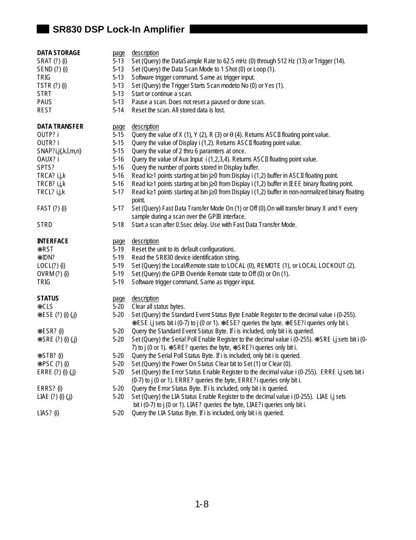
DATA STORAGE page descriptionSRAT (?) i 5-13 Set (Query) the DataSample Rate to 62.5 mHz (0) through 512 Hz (13) or Trigger (14).SEND (?) i 5-13 Set (Query) the Data Scan Mode to 1 Shot (0) or Loop (1). TRIG 5-13 Software trigger command. Same as trigger input.TSTR (?) i 5-13 Set (Query) the Trigger Starts Scan modeto No (0) or Yes (1).STRT 5-13 Start or continue a scan. PAUS 5-13 Pause a scan. Does not reset a paused or done scan.REST 5-14 Reset the scan. All stored data is lost.
DATA TRANSFER page descriptionOUTP? i 5-15 Query the value of X (1), Y (2), R (3) or θ (4). Returns ASCII floating point value.OUTR? i 5-15 Query the value of Display i (1,2). Returns ASCII floating point value.SNAP?i,j,k,l,m,n 5-15 Query the value of 2 thru 6 paramters at once.OAUX? i 5-16 Query the value of Aux Input i (1,2,3,4). Returns ASCII floating point value.SPTS? 5-16 Query the number of points stored in Display buffer.TRCA? i,j,k 5-16 Read k≥1 points starting at bin j≥0 from Display i (1,2) buffer in ASCII floating point.TRCB? i,j,k 5-16 Read k≥1 points starting at bin j≥0 from Display i (1,2) buffer in IEEE binary floating point.TRCL? i,j,k 5-17 Read k≥1 points starting at bin j≥0 from Display i (1,2) buffer in non-normalized binary floating
point.FAST (?) i 5-17 Set (Query) Fast Data Transfer Mode On (1) or Off (0).On will transfer binary X and Y every
sample during a scan over the GPIB interface.STRD 5-18 Start a scan after 0.5sec delay. Use with Fast Data Transfer Mode.
INTERFACE page descriptionRST 5-19 Reset the unit to its default configurations.IDN? 5-19 Read the SR830 device identification string.LOCL(?) i 5-19 Set (Query) the Local/Remote state to LOCAL (0), REMOTE (1), or LOCAL LOCKOUT (2).OVRM (?) i 5-19 Set (Query) the GPIB Overide Remote state to Off (0) or On (1).TRIG 5-19 Software trigger command. Same as trigger input.
STATUS page descriptionCLS 5-20 Clear all status bytes.ESE (?) i ,j 5-20 Set (Query) the Standard Event Status Byte Enable Register to the decimal value i (0-255).
ESE i,j sets bit i (0-7) to j (0 or 1). ESE? queries the byte. ESE?i queries only bit i.ESR? i 5-20 Query the Standard Event Status Byte. If i is included, only bit i is queried.SRE (?) i ,j 5-20 Set (Query) the Serial Poll Enable Register to the decimal value i (0-255). SRE i,j sets bit i (0-
7) to j (0 or 1). SRE? queries the byte, SRE?i queries only bit i.STB? i 5-20 Query the Serial Poll Status Byte. If i is included, only bit i is queried.PSC (?) i 5-20 Set (Query) the Power On Status Clear bit to Set (1) or Clear (0).ERRE (?) i ,j 5-20 Set (Query) the Error Status Enable Register to the decimal value i (0-255). ERRE i,j sets bit i
(0-7) to j (0 or 1). ERRE? queries the byte, ERRE?i queries only bit i.ERRS? i 5-20 Query the Error Status Byte. If i is included, only bit i is queried.LIAE (?) i ,j 5-20 Set (Query) the LIA Status Enable Register to the decimal value i (0-255). LIAE i,j sets
bit i (0-7) to j (0 or 1). LIAE? queries the byte, LIAE?i queries only bit i.LIAS? i 5-20 Query the LIA Status Byte. If i is included, only bit i is queried.
SR830 DSP Lock-In Amplifier
1-9
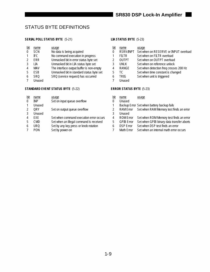
SERIAL POLL STATUS BYTE (5-21)
bit name usage0 SCN No data is being acquired1 IFC No command execution in progress2 ERR Unmasked bit in error status byte set3 LIA Unmasked bit in LIA status byte set4 MAV The interface output buffer is non-empty5 ESB Unmasked bit in standard status byte set6 SRQ SRQ (service request) has occurred7 Unused
STANDARD EVENT STATUS BYTE (5-22)
bit name usage0 INP Set on input queue overflow1 Unused2 QRY Set on output queue overflow 3 Unused4 EXE Set when command execution error occurs5 CMD Set when an illegal command is received6 URQ Set by any key press or knob rotation7 PON Set by power-on
LIA STATUS BYTE (5-23)
bit name usage0 RSRV/INPT Set when on RESERVE or INPUT overload1 FILTR Set when on FILTR overload2 OUTPT Set when on OUTPT overload3 UNLK Set when on reference unlock4 RANGE Set when detection freq crosses 200 Hz5 TC Set when time constant is changed6 TRIG Set when unit is triggered7 Unused
ERROR STATUS BYTE (5-23)
bit name usage0 Unused1 Backup Error Set when battery backup fails2 RAM Error Set when RAM Memory test finds an error3 Unused4 ROM Error Set when ROM Memory test finds an error5 GPIB Error Set when GPIB binary data transfer aborts6 DSP Error Set when DSP test finds an error7 Math Error Set when an internal math error occurs
STATUS BYTE DEFINITIONS

SR830 DSP Lock-In Amplifier
1-10
GETTING STARTED
The sample measurements described in this section are designed to acquaint the first time user with theSR830 DSP Lock-In Amplifier. Do not be concerned that your measurements do not exactly agree with theseexercises. The focus of these measurement exercises is to learn how to use the instrument.
It is highly recommended that the first time user step through some or all of these exercises before attemptingto perform an actual experiment.
The experimental procedures are detailed in two columns. The left column lists the actual steps in the experi-ment. The right column is an explanation of each step.
[Keys] Front panel keys are referred to in brackets such as [Display] where'Display' is the key label.
Knob The knob is used to adjust parameters which are displayed in theReference display.
2-1
YOUR FIRST MEASUREMENTS

2-2
Getting Started
2-3
THE BASIC LOCK-INThis measurement is designed to use the internal oscillator to explore some of the basic lock-in functions.You will need BNC cables.
Specifically, you will measure the amplitude of the Sine Out at various frequencies, sensitivities, time con-stants and phase shifts.
1. Disconnect all cables from the lock-in. Turnthe power on while holding down the [Setup]key. Wait until the power-on tests arecompleted.
2. Connect the Sine Out on the front panel to theA input using a BNC cable.
3. Press [Auto Phase]
4. Press [Phase]
5. Press the [+90°] key.
When the power is turned on with the [Setup] keypressed, the lock-in returns to its standard defaultsettings. See the Standard Settings list in theOperation section for a complete listing of thesettings.
The Channel 1 display shows X and Channel 2shows Y.
The lock-in defaults to the internal oscillator refer-ence set at 1.000 kHz. The reference mode is indi-cated by the INTERNAL led. In this mode, thelock-in generates a synchronous sine output at theinternal reference frequency.
The input impedance of the lock-in is 10 MΩ. TheSine Out has an output impedance of 50Ω. Sincethe Sine Output amplitude is specified into a highimpedance load, the output impedance does notaffect the amplitude.
The sine amplitude is 1.000 Vrms and the sensitivity is 1 V(rms). Since the phase shift of thesine output is very close to zero, Channel 1 (X)should read close to 1.000 V and Channel 2 (Y)should read close to 0.000 V.
Automatically adjust the reference phase shift toeliminate any residual phase error. This should setthe value of Y to zero.
Display the reference phase shift in the Referencedisplay. The phase shift should be close to zero.
This adds 90° to the reference phase shift. Thevalue of X drops to zero and Y becomes minus themagnitude (-1.000 V).
The Basic Lock-in
2-4
Use the knob to adjust the phase shift until Yis zero and X is equal to the positiveamplitude.
Press [Auto Phase]
6. Press [Freq]
Use the knob to adjust the frequency to10 kHz.
Use the knob to adjust the frequency back to1 kHz.
7. Press [Ampl]
Use the knob to adjust the amplitude to0.01 V.
8. Press [Auto Gain]
9. Press [Sensitivity Up] to select 50 mV fullscale.
Change the sensitivity back to 20 mV.
10. Press [Time Constant Down] to change thetime constant to 300 µs.
Press [Time Constant Up] to change the timeconstant to 3 ms.
The knob is used to adjust parameters which areshown in the Reference display, such as phase,amplitude and frequency. The final phase valueshould be close to zero again.
Use the Auto Phase function to return Y to zeroand X to the amplitude.
Show the internal oscillator frequency in theReference display.
The knob now adjusts the frequency. The meas-ured signal amplitude should stay within 1% of 1 Vand the phase shift should stay close to zero (thevalue of Y should stay close to zero).
The internal oscillator is crystal synthesized with25 ppm of frequency error. The frequency can beset with 4 1/2 digit or 0.1 mHz resolution, whichev-er is greater.
Show the sine output amplitude in the Referencedisplay.
As the amplitude is changed, the measured valueof X should equal the sine output amplitude. Thesine amplitude can be set from 4 mV to 5 V rmsinto high impedance (half the amplitude into a 50Ω load).
The Auto Gain function will adjust the sensitivity sothat the measured magnitude (R) is a sizable per-centage of full scale. Watch the sensitivity indica-tors change.
Parameters which have many options, such assensitivity and time constant, are changed with upand down keys. The sensitivity and time constantare indicated by leds.
The values of X and Y become noisy. This isbecause the 2f component of the output (at 2 kHz)is no longer attenuated completely by the low passfilters.
Let's leave the time constant short and change thefilter slope.
The Basic Lock-in
2-5
11. Press the [Slope/Oct] key until 6 dB/oct isselected.
Press [Slope/Oct] again to select 12 dB/oct.
Press [Slope/Oct] twice to select 24 db/oct.
Press [Slope/Oct] again to select 6 db/oct.
12. Press [Freq]
Use the knob to adjust the frequency to55.0 Hz.
13. Press [Sync Filter]
Parameters which have only a few values, such asfilter slope, have only a single key which cyclesthrough all available options. Press the corre-sponding key until the desired option is indicatedby an led.
The X and Y outputs are somewhat noisy at thisshort time constant and only 1 pole of low passfiltering.
The outputs are less noisy with 2 poles of filtering.
With 4 poles of low pass filtering, even this shorttime constant attenuates the 2f component rea-sonably well and provides steady readings.
Let's leave the filtering short and the outputs noisyfor now.
Show the internal reference frequency on theReference display.
At a reference frequency of 55 Hz and a 6 db/oct,3 ms time constant, the output is totally dominatedby the 2f component at 100 Hz.
This turns on synchronous filtering whenever thedetection frequency is below 200 Hz.
Synchronous filtering effectively removes outputcomponents at multiples of the detection frequen-cy. At low frequencies, this filter is a very effectiveway to remove 2f without using extremely longtime constants.
The outputs are now very quiet and steady, eventhough the time constant is very short. Theresponse time of the synchronous filter is equal tothe period of the detection frequency (18 ms in thiscase).
This concludes this measurement example. Youshould have a feeling for the basic operation of thefront panel. Basic lock-in parameters have beenintroduced and you should be able to performsimple measurements.
The Basic Lock-in

2-6
The Basic Lock-in
2-7
X, Y, R and θThis measurement is designed to use the internal oscillator and an external signal source to explore some ofthe display types. You will need a synthesized function generator capable of providing a 100 mVrms sinewave at 1.000 kHz (the DS335 from SRS will suffice), BNC cables and a terminator appropriate for the gener-ator function output.
Specifically, you will display the lock-in outputs when measuring a signal close to, but not equal to, the inter-nal reference frequency. This setup ensures changing outputs which are more illustrative than steady outputs.The displays will be configured to show X, Y, R and θ.
1. Disconnect all cables from the lock-in. Turnthe power on while holding down the [Setup]key. Wait until the power-on tests arecompleted.
2. Turn on the function generator, set the fre-quency to 1.0000 kHz (exactly) and the ampli-tude to 500 mVrms.
Connect the function output (sine wave) fromthe synthesized function generator to the Ainput using a BNC cable and appropriateterminator.
3. Press [Freq]
Use the knob to change the frequency to999.8 Hz.
When the power is turned on with the [Setup] keypressed, the lock-in returns to its standard set-tings. See the Standard Settings list in theOperation section for a complete listing of thesettings.
The Channel 1 display shows X and Channel 2shows Y.
The input impedance of the lock-in is 10 MΩ. Thegenerator may require a terminator. Many genera-tors have either a 50Ω or 600Ω output impedance.Use the appropriate feedthrough or T termination ifnecessary. In general, not using a terminatormeans that the function output amplitude will notagree with the generator setting.
The lock-in defaults to the internal oscillator refer-ence set at 1.000 kHz. The reference mode is indi-cated by the INTERNAL led. In this mode, theinternal oscillator sets the detection frequency.
The internal oscillator is crystal synthesized sothat the actual reference frequency should be veryclose to the actual generator frequency. The X andY displays should read values which change veryslowly. The lock-in and the generator are notphase locked but they are at the same frequencywith some slowly changing phase.
Show the internal oscillator frequency on theReference display.
By setting the lock-in reference 0.2 Hz away fromthe signal frequency, the X and Y outputs are0.2 Hz sine waves (frequency difference betweenreference and signal). The X and Y output displays
X, Y, R and θ
2-8
X, Y, R and θ
should now oscillate at about 0.2 Hz (the accuracyis determined by the crystals of the generator andthe lock-in).
The default Channel 1 display is X. Change thedisplay to show R. R is phase independent so itshows a steady value (close to 0.500 V).
The default Channel 2 display is Y. Change thedisplay to show θ. The phase between the refer-ence and the signal changes by 360° approximate-ly every 5 sec (0.2 Hz difference frequency).
The bar graph in this case is scaled to ±180°. Thebar graph should be a linear phase ramp at0.2 Hz.
Show the internal oscillator frequency.
As the internal reference frequency gets closer tothe signal frequency, the phase rotation getsslower and slower. If the frequencies areEXACTLY equal, then the phase is constant.
By using the signal generator as the external refer-ence, the lock-in will phase lock its internal oscilla-tor to the signal frequency and the phase will be aconstant.
Select external reference mode. The lock-in willphase lock to the signal at the Reference Input.
With a TTL reference signal, the slope needs to beset to either rising or falling edge.
The phase is now constant. The actual phasedepends upon the phase difference between thefunction output and the sync output from thegenerator.
The external reference frequency (as measured bythe lock-in) is displayed on the Reference display.The UNLOCK indicator should be OFF (success-fully locked to the external reference).
The displays may be stored in the internal databuffers at a programmable sampling rate. Thisallows storage of 16000 points of both displays.
4. Press [Channel 1 Display] to select R.
5. Press [Channel 2 Display] to select θ.
6. Press [Freq]
Use the knob to adjust the frequency slowly totry to stop the rotation of the phase.
7. Use a BNC cable to connect the TTL SYNCoutput from the generator to the ReferenceInput of the lock-in.
Press [Source] to turn the INTERNAL led off.
Press [Trig] to select POS EDGE.
2-9
OUTPUTS, OFFSETS and EXPANDSThis measurement is designed to use the internal oscillator to explore some of the basic lock-in outputs. Youwill need BNC cables and a digital voltmeter (DVM).
Specifically, you will measure the amplitude of the Sine Out and provide analog outputs proportional to themeasurement. The effect of offsets and expands on the displayed values and the analog outputs will beexplored.
1. Disconnect all cables from the lock-in. Turnthe power on while holding down the [Setup]key. Wait until the power-on tests arecompleted.
2. Connect the Sine Out on the front panel to theA input using a BNC cable.
3. Connect the CH1 OUTPUT on the front panelto the DVM. Set the DVM to read DC Volts.
4. Press [Ampl]
Use the knob to adjust the sine amplitude to0.5 V.
When the power is turned on with the [Setup] keypressed, the lock-in returns to its standard set-tings. See the Standard Settings list in theOperation section for a complete listing of thesettings.
The Channel 1 display shows X and Channel 2shows Y.
The lock-in defaults to the internal oscillator refer-ence set at 1.000 kHz. The reference mode is indi-cated by the INTERNAL led. In this mode, thelock-in generates a synchronous sine output at theinternal reference frequency.
The input impedance of the lock-in is 10 MΩ. TheSine Out has an output impedance of 50Ω. Sincethe Sine Output amplitude is specified into a highimpedance load, the output impedance does notaffect the amplitude.
The sine amplitude is 1.000 Vrms and the sensitivity is 1 V(rms). Since the phase shift of thesine output is very close to zero, Channel 1 (X)should read close to 1.000 V and Channel 2 (Y)should read close to 0.000 V.
The CH1 output defaults to X. The output voltageis simply (X/Sensitivity - Offset)xExpandx10V. Inthis case, X = 1.000 V, the sensitivity = 1 V, theoffset is zero percent and the expand is 1. Theoutput should thus be 10 V or 100% of full scale.
Display the sine output amplitude.
Set the amplitude to 0.5 V. The Channel 1 displayshould show X=0.5 V and the CH1 output voltageshould be 5 V on the DVM (1/2 of full scale).
Outputs, Offsets and Expands
2-10
5. Press [Channel 1 Auto Offset]
Press [Channel 1 Offset Modify]
Use the knob to adjust the X offset to 40.0%
Press [Channel 1 Expand] to select x10.
X, Y and R may all be offset and expanded separ-ately. Since Channel 1 is displaying X, theOFFSET and [Expand] keys below the Channel 1display set the X offset and expand. The displaydetermines which quantity (X or R) is offset andexpanded.
Auto Offset automatically adjusts the X offset (or Yor R) such that X (or Y or R) becomes zero. In thiscase, X is offset to zero. The offset should beabout 50%. Offsets are useful for making relativemeasurements. In analog lock-ins, offsets weregenerally used to remove DC output errors fromthe lock-in itself. The SR830 has no DC outputerrors and the offset is not required for mostmeasurements.
The offset affects both the displayed value of Xand any analog output proportional to X. The CH1output voltage should be zero in this case.
The Offset indicator turns on at the bottom of theChannel 1 display to indicate that the displayedquantity is affected by an offset.
Show the Channel 1 (X) offset in the Referencedisplay.
Change the offset to 40% of full scale. The outputoffsets are a percentage of full scale. The percent-age does not change with the sensitivity. The dis-played value of X should be 0.100 V (0.5 V - 40%of full scale). The CH1 output voltage is(X/Sensitivity - Offset)xExpandx10V.
CH1 Out = (0.5/1.0 - 0.4)x1x10V = 1 V
With an expand of 10, the display has one moredigit of resolution (100.00 mV full scale).
The Expand indicator turns on at the bottom of theChannel 1 display to indicate that the displayedquantity is affected by a non-unity expand.
The CH1 output is(X/Sensitivity - Offset)xExpandx10V. In this case,the output voltage is
CH1 Out = (0.5/1.0 - 0.4)x10x10V = 10V
The expand allows the output gain to be increasedby up to 100. The output voltage is limited to10.9 V and any output which tries to be greater will
Outputs, Offsets and Expands
2-11
6. Connect the DVM to the X output on the rearpanel.
7. Connect the DVM to the CH1 OUTPUT on thefront panel again.
Press [Channel 1 Output] to select Display.
Press [Channel 1 Display] to select R.
turn on the OVLD indicator in the Channel 1display.
With offset and expand, the output voltage gainand offset can be programmed to provide controlof feedback signals with the proper bias and gainfor a variety of situations.
Offsets add and subtract from the displayedvalues while expand increases the resolution ofthe display.
The X and Y outputs on the rear panel always pro-vide voltages proportional to X and Y (with offsetand expand). The X output voltage should be10 V, just like the CH1 output.
The front panel outputs can be configured tooutput different quantities while the rear panel out-puts always output X and Y.
NOTE:Outputs proportional to X and Y (rear panel, CH1or CH2) have 100 kHz of bandwidth. The CH1 andCH2 outputs, when configured to be proportionalto the displays (even if the display is X or Y) areupdated at 512 Hz and have a 200 Hz bandwidth.It is important to keep this in mind if you use veryshort time constants.
CH1 OUTPUT can be proportional to X or the dis-play. Choose Display. The display is X so the CH1output should remain 10.0 V (but its bandwidth isonly 200 Hz instead of 100 kHz).
Let's change CH1 to output R.
The X and Y offset and expand functions areoutput functions, they do NOT affect the calcula-tion of R or θ. Thus, Channel 1 (R) should be 0.5Vand the CH1 output voltage should be 5V (1/2 offull scale).
The Channel 1 offset and expand keys now setthe R offset and expand. The X offset and expandare still set at 40% and x10 as reflected at the rearpanel X output.
See the DC Outputs and Scaling discussion in theLock-In Basics section for more detailed informa-tion on output scaling.
Outputs, Offsets and Expands

2-12
Outputs, Offsets and Expands
2-13
STORING and RECALLING SETUPSThe SR830 can store 9 complete instrument setups in non-volatile memory.
When the power is turned on with the [Setup] keypressed, the lock-in returns to its standard set-tings. See the Standard Settings list in theOperation section for a complete listing of thesettings.
Change the lock-in setup so that we have a non-default setup to save.
Change the sensitivity to 100 mV.
Change the time constant to 1 second.
The Reference display shows the setup number(1-9).
The knob selects the setup number.
Press [Save] again to complete the save opera-tion. Any other key aborts the save.
The current setup is now saved as setup number3.
Change the lock-in setup back to the defaultsetup. Now let's recall the lock-in setup that wejust saved.
Check that the sensitivity and time constant are 1Vand 100 ms (default values).
The Reference display shows the setup number.
The knob selects the setup number.
Press [Recall] again to complete the recall opera-tion. Any other key aborts the recall.
The sensitivity and time constant should be thesame as those in effect when the setup wassaved.
Storing and Recalling Setups
1. Turn the lock-in on while holding down the[Setup] key. Wait until the power-on tests arecompleted. Disconnect any cables from thelock-in.
2. Press [Sensitivity Down] to select 100 mV.
Press [Time Constant Up] to select 1 S.
3. Press [Save]
Use the knob to select setup number 3.
Press [Save] again.
4. Turn the lock-in off and on while holding downthe [Setup] key. Wait until the power-on testsare complete.
5. Press [Recall]
Use the knob to select setup number 3.
Press [Recall] again.

2-14
Storing and Recalling Setups
2-15
AUX OUTPUTS and INPUTSThis measurement is designed to illustrate the use of the Aux Outputs and Inputs on the rear panel. You willneed BNC cables and a digital voltmeter (DVM).
Specifically, you will set the Aux Output voltages and measure them with the DVM. These outputs will then beconnected to the Aux Inputs to simulate external DC voltages which the lock-in can measure.
1. Disconnect all cables from the lock-in. Turnthe power on while holding down the [Setup]key. Wait until the power-on tests arecompleted.
2. Connect Aux Out 1 on the rear panel to theDVM. Set the DVM to read DC volts.
3. Press [Aux Out] until the Reference displayshows the level of Aux Out 1( as indicated bythe AxOut1 led below the display).
Use the knob to adjust the level to 10.00 V.
Use the knob to adjust the level to -5.00 V.
4. Press [Channel 1 Display] to select AUX IN 1.
5. Disconnect the DVM from Aux Out 1. ConnectAuxOut 1 to Aux In 1 on the rear panel.
When the power is turned on with the [Setup] keypressed, the lock-in returns to its standard set-tings. See the Standard Settings list in theOperation section for a complete listing of thesettings.
The 4 Aux Outputs can provide programmablevoltages between -10.5 and +10.5 volts. The out-puts can be set from the front panel or via thecomputer interface.
Show the level of Aux Out 1 on the Referencedisplay.
Change the output to 10V. The DVM should dis-play 10.0 V.
Change the output to -5V. The DVM should dis-play -5.0 V.
The 4 outputs are useful for controlling otherparameters in an experiment, such as pressure,temperature, wavelength, etc.
Change the Channel 1 display to measure AuxInput 1.
The Aux Inputs can read 4 analog voltages. Theseinputs are useful for monitoring and measuringother parameters in an experiment, such as pres-sure, temperature, position, etc.
We'll use Aux Out 1 to provide an analog voltageto measure.
Channel 1 should now display -5 V (Aux In 1).
Aux Outputs and Inputs
2-16
6. Press [Channel 2 Display] to select AUX IN 3.
7. Connect Aux Out 1 to Aux In 3 on the rearpanel.
Change the Channel 2 display to measure AuxInput 3.
Channel 2 should now display -5 V (Aux In 3).
The Channel 1 and 2 displays may be ratio'ed tothe Aux Input voltages. See the Basics section formore about output scaling.
The displays may be stored in the internal databuffers at a programmable sampling rate. Thisallows storage of not only the lock-in outputs, X,Y,R or θ, but also the values of the Aux Inputs. Seethe Programming section for more details.
Aux Outputs and Inputs
SR830 BASICS
Lock-in amplifiers are used to detect and measurevery small AC signals - all the way down to a fewnanovolts! Accurate measurements may be madeeven when the small signal is obscured by noisesources many thousands of times larger.
Lock-in amplifiers use a technique known asphase-sensitive detection to single out the compo-nent of the signal at a specific reference frequencyAND phase. Noise signals at frequencies otherthan the reference frequency are rejected and donot affect the measurement.
Why use a lock-in? Let's consider an example. Suppose the signal is a10 nV sine wave at 10 kHz. Clearly some amplifi-cation is required. A good low noise amplifier willhave about 5 nV/√Hz of input noise. If the amplifierbandwidth is 100 kHz and the gain is 1000, thenwe can expect our output to be 10 µV of signal(10 nV x 1000) and 1.6 mV of broadband noise(5 nV/√Hz x √100 kHz x 1000). We won't havemuch luck measuring the output signal unless wesingle out the frequency of interest.
If we follow the amplifier with a band pass filterwith a Q=100 (a VERY good filter) centered at10 kHz, any signal in a 100 Hz bandwidth will bedetected (10 kHz/Q). The noise in the filter passband will be 50 µV (5 nV/√Hz x √100 Hz x 1000)and the signal will still be 10 µV. The output noiseis much greater than the signal and an accuratemeasurement can not be made. Further gain willnot help the signal to noise problem.
Now try following the amplifier with a phase-sensitive detector (PSD). The PSD can detect thesignal at 10 kHz with a bandwidth as narrow as0.01 Hz! In this case, the noise in the detectionbandwidth will be only 0.5 µV (5 nV/√Hz x √.01 Hzx 1000) while the signal is still 10 µV. The signal tonoise ratio is now 20 and an accurate measure-ment of the signal is possible.
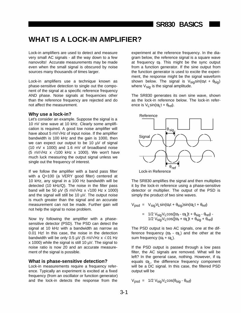
What is phase-sensitive detection?Lock-in measurements require a frequency refer-ence. Typically an experiment is excited at a fixedfrequency (from an oscillator or function generator)and the lock-in detects the response from the
experiment at the reference frequency. In the dia-gram below, the reference signal is a square waveat frequency ωr. This might be the sync outputfrom a function generator. If the sine output fromthe function generator is used to excite the experi-ment, the response might be the signal waveformshown below. The signal is Vsigsin(ωrt + θsig)where Vsig is the signal amplitude.
The SR830 generates its own sine wave, shownas the lock-in reference below. The lock-in refer-ence is VLsin(ωLt + θref).
The SR830 amplifies the signal and then multipliesit by the lock-in reference using a phase-sensitivedetector or multiplier. The output of the PSD issimply the product of two sine waves.
Vpsd = VsigVLsin(ωrt + θsig)sin(ωLt + θref)
= 1/2 VsigVLcos([ωr - ωL]t + θsig - θref) -1/2 VsigVLcos([ωr + ωL]t + θsig + θref)
The PSD output is two AC signals, one at the dif-ference frequency (ωr - ωL) and the other at thesum frequency (ωr + ωL).
If the PSD output is passed through a low passfilter, the AC signals are removed. What will beleft? In the general case, nothing. However, if ωrequals ωL, the difference frequency componentwill be a DC signal. In this case, the filtered PSDoutput will be
Vpsd = 1/2 VsigVLcos(θsig - θref)
WHAT IS A LOCK-IN AMPLIFIER?
3-1
θ ref
Reference
Signal
Lock-in Reference
sigθ
3-2
SR830 Basics
This is a very nice signal - it is a DC signal propor-tional to the signal amplitude.
Narrow band detectionNow suppose the input is made up of signal plusnoise. The PSD and low pass filter only detect sig-nals whose frequencies are very close to the lock-in reference frequency. Noise signals at frequen-cies far from the reference are attenuated at thePSD output by the low pass filter (neither ωnoise-ωref nor ωnoise+ωref are close to DC). Noise at fre-quencies very close to the reference frequency willresult in very low frequency AC outputs from thePSD (|ωnoise-ωref| is small). Their attenuationdepends upon the low pass filter bandwidth androll-off. A narrower bandwidth will remove noisesources very close to the reference frequency, awider bandwidth allows these signals to pass. Thelow pass filter bandwidth determines the band-width of detection. Only the signal at the referencefrequency will result in a true DC output and beunaffected by the low pass filter. This is the signalwe want to measure.
Where does the lock-in reference come from?We need to make the lock-in reference the sameas the signal frequency, i.e. ωr = ωL. Not only dothe frequencies have to be the same, the phasebetween the signals can not change with time, oth-erwise cos(θsig - θref) will change and Vpsd will notbe a DC signal. In other words, the lock-in refer-ence needs to be phase-locked to the signalreference.
Lock-in amplifiers use a phase-locked-loop (PLL)to generate the reference signal. An external refer-ence signal (in this case, the reference squarewave) is provided to the lock-in. The PLL in thelock-in locks the internal reference oscillator to thisexternal reference, resulting in a reference sinewave at ωr with a fixed phase shift of θref. Sincethe PLL actively tracks the external reference,changes in the external reference frequency donot affect the measurement.
All lock-in measurements require a reference signal. In this case, the reference is provided by the exci-tation source (the function generator). This iscalled an external reference source. In many situa-tions, the SR830's internal oscillator may be usedinstead. The internal oscillator is just like a func-tion generator (with variable sine output and a TTL
sync) which is always phase-locked to the refer-ence oscillator.
Magnitude and phaseRemember that the PSD output is proportionalto Vsigcosθ where θ = (θsig - θref). θ is the phasedifference between the signal and the lock-in refer-ence oscillator. By adjusting θref we can make θequal to zero, in which case we can measure Vsig(cosθ=1). Conversely, if θ is 90°, there will be nooutput at all. A lock-in with a single PSD is called asingle-phase lock-in and its output is Vsigcosθ.
This phase dependency can be eliminated byadding a second PSD. If the second PSD multi-plies the signal with the reference oscillator shiftedby 90°, i.e. VLsin(ωLt + θref + 90°), its low pass fil-tered output will be
Vpsd2 = 1/2 VsigVLsin(θsig - θref)
Vpsd2 ~ Vsigsinθ
Now we have two outputs, one proportional tocosθ and the other proportional to sinθ. If we callthe first output X and the second Y,
X = Vsigcosθ Y = Vsigsinθ
these two quantities represent the signal as avector relative to the lock-in reference oscillator. Xis called the 'in-phase' component and Y the'quadrature' component. This is because whenθ=0, X measures the signal while Y is zero.
By computing the magnitude (R) of the signalvector, the phase dependency is removed.
R = (X2 + Y2)1/2 = Vsig
R measures the signal amplitude and does notdepend upon the phase between the signal andlock-in reference.
A dual-phase lock-in, such as the SR830, has twoPSD's, with reference oscillators 90° apart, andcan measure X, Y and R directly. In addition, thephase θ between the signal and lock-in reference,can be measured according to
θ = tan-1 (Y/X)
3-3
SR830 Basics
So what exactly does the SR830 measure?Fourier's theorem basically states that any inputsignal can be represented as the sum of many,many sine waves of differing amplitudes, frequen-cies and phases. This is generally considered asrepresenting the signal in the "frequency domain".Normal oscilloscopes display the signal in the"time domain". Except in the case of clean sinewaves, the time domain representation does notconvey very much information about the variousfrequencies which make up the signal.
What does the SR830 measure? The SR830 multiplies the signal by a pure sinewave at the reference frequency. All componentsof the input signal are multiplied by the referencesimultaneously. Mathematically speaking, sinewaves of differing frequencies are orthogonal, i.e.the average of the product of two sine waves iszero unless the frequencies are EXACTLY thesame. In the SR830, the product of this multiplica-tion yields a DC output signal proportional to thecomponent of the signal whose frequency is exact-ly locked to the reference frequency. The low passfilter which follows the multiplier provides the aver-aging which removes the products of the referencewith components at all other frequencies.
The SR830, because it multiplies the signal with apure sine wave, measures the single Fourier (sine)component of the signal at the reference frequen-cy. Let's take a look at an example. Suppose theinput signal is a simple square wave at frequencyf. The square wave is actually composed of manysine waves at multiples of f with carefully relatedamplitudes and phases. A 2V pk-pk square wavecan be expressed as
S(t) = 1.273sin(ωt) + 0.4244sin(3ωt) + 0.2546sin(5ωt) + ...
where ω = 2πf. The SR830, locked to f will singleout the first component. The measured signal willbe 1.273sin(ωt), not the 2V pk-pk that you'd meas-ure on a scope.
In the general case, the input consists of signalplus noise. Noise is represented as varying signalsat all frequencies. The ideal lock-in only respondsto noise at the reference frequency. Noise at other
WHAT DOES A LOCK-IN MEASURE?
frequencies is removed by the low pass filter fol-lowing the multiplier. This "bandwidth narrowing" isthe primary advantage that a lock-in amplifier pro-vides. Only inputs at frequencies at the referencefrequency result in an output.
RMS or Peak?Lock-in amplifiers as a general rule display theinput signal in Volts RMS. When the SR830 dis-plays a magnitude of 1V (rms), the component ofthe input signal at the reference frequency is asine wave with an amplitude of 1 Vrms or2.8 V pk-pk.
Thus, in the previous example with a 2 V pk-pksquare wave input, the SR830 would detect thefirst sine component, 1.273sin(ωt). The measuredand displayed magnitude would be 0.90 V (rms)(1/√2 x 1.273).
Degrees or Radians?In this discussion, frequencies have been referredto as f (Hz) and ω (2πf radians/sec). This isbecause people measure frequencies in cyclesper second and math works best in radians. Forpurposes of measurement, frequencies as meas-ured in a lock-in amplifier are in Hz. The equationsused to explain the actual calculations are some-times written using ω to simplify the expressions.
Phase is always reported in degrees. Once again,this is more by custom than by choice. Equationswritten as sin(ωt + θ) are written as if θ is inradians mostly for simplicity. Lock-in amplifiersalways manipulate and measure phase indegrees.

3-4
SR830 Basics
3-5
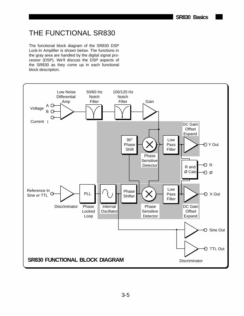
SR830 Basics
The functional block diagram of the SR830 DSPLock-In Amplifier is shown below. The functions inthe gray area are handled by the digital signal pro-cessor (DSP). We'll discuss the DSP aspects ofthe SR830 as they come up in each functionalblock description.
THE FUNCTIONAL SR830
Phase Sensitive Detector
PLL
I
A
B
Low NoiseDifferential
Amp
Voltage
Current
50/60 Hz Notch Filter
Reference InSine or TTL
PhaseShifter
DC GainOffset
Expand
Gain
X Out
Y Out
Discriminator
100/120 Hz NotchFilter
90° PhaseShift
Phase Locked Loop
Internal Oscillator
Low PassFilter
DC GainOffset
Expand
Low PassFilter
Sine Out
Discriminator
TTL Out
R and Ø Calc
R
Ø
Phase Sensitive Detector
SR830 FUNCTIONAL BLOCK DIAGRAM

3-6
SR830 Basics
3-7
SR830 Basics
A lock-in amplifier requires a reference oscillatorphase-locked to the signal frequency. In general,this is accomplished by phase-locking an internaloscillator to an externally provided referencesignal. This reference signal usually comes fromthe signal source which is providing the excitationto the experiment.
Reference InputThe SR830 reference input can trigger on ananalog signal (like a sine wave) or a TTL logicsignal. The first case is called External Sine. Theinput is AC coupled (above 1 Hz) and the inputimpedance is 1 MΩ. A sine wave input greaterthan 200 mV pk will trigger the input discriminator.Positive zero crossings are detected and consid-ered to be the zero for the reference phase shift.
TTL reference signals can be used at all frequen-cies up to 102 kHz. For frequencies below 1 Hz,a TTL reference signal is required. Many func-tion generators provide a TTL SYNC output whichcan be used as the reference. This is convenientsince the generator's sine output might be smallerthan 200 mV or be varied in amplitude. The SYNCsignal will provide a stable reference regardless ofthe sine amplitude.
When using a TTL reference, the reference inputtrigger can be set to Pos Edge (detect risingedges) or Neg Edge (detect falling edges). In eachcase, the internal oscillator is locked (at zerophase) to the detected edge.
Internal OscillatorThe internal oscillator in the SR830 is basically a102 kHz function generator with sine and TTLsync outputs. The oscillator can be phase-lockedto the external reference.
The oscillator generates a digitally synthesizedsine wave. The digital signal processor, or DSP,sends computed sine values to a 16 bit digital-to-analog converter every 4 µs (256 kHz). An anti-aliasing filter converts this sampled signal into alow distortion sine wave. The internal oscillatorsine wave is output at the SINE OUT BNC on thefront panel. The amplitude of this output may beset from 4 mV to 5 V.
REFERENCE CHANNEL
When an external reference is used, this internaloscillator sine wave is phase-locked to the refer-ence. The rising zero crossing is locked to thedetected reference zero crossing or edge. In thismode, the SINE OUT provides a sine wave phase-locked to the external reference. At low frequen-cies (below 10 Hz), the phase locking is accom-plished digitally by the DSP. At higher frequencies,a discrete phase comparator is used.
The internal oscillator may be used without anexternal reference. In the Internal Referencemode, the SINE OUT provides the excitation forthe experiment. The phase-locked-loop is not usedin this mode since the lock-in reference is provid-ing the excitation signal.
The TTL OUT on the rear panel provides a TTLsync output. The internal oscillator's rising zerocrossings are detected and translated to TTLlevels. This output is a square wave.
Reference Oscillators and PhaseThe internal oscillator sine wave is not the refer-ence signal to the phase sensitive detectors. TheDSP computes a second sine wave, phase shiftedby θref from the internal oscillator (and thus froman external reference), as the reference input tothe X phase sensitive detector. This waveform issin(ωrt + θref). The reference phase shift is adjust-able in .01° increments.
The input to the Y PSD is a third sine wave, com-puted by the DSP, shifted by 90° from the secondsine wave. This waveform is sin(ωrt + θref + 90°).
Both reference sine waves are calculated to 20bits of accuracy and a new point is calculatedevery 4 µs (256 kHz). The phase shifts (θref andthe 90° shift) are also exact numbers and accurateto better than .001°. Neither waveform is actuallyoutput in analog form since the phase sensitivedetectors are actually multiply instructions insidethe DSP.
Phase JitterWhen an external reference is used, the phase-locked loop adds a little phase jitter. The internaloscillator is supposed to be locked with zerophase shift relative the external reference. Phase
3-8
SR830 Basics
jitter means that the average phase shift is zerobut the instantaneous phase shift has a few milli-degrees of noise. This shows up at the output asnoise in phase or quadrature measurements.
Phase noise can also cause noise to appear at theX and Y outputs. This is because a referenceoscillator with a lot of phase noise is the same asa reference whose frequency spectrum is spreadout. That is, the reference is not a single frequen-cy, but a distribution of frequencies about the truereference frequency. These spurious frequenciesare attenuated quite a bit but still cause problems.The spurious reference frequencies result in sig-nals close to the reference being detected. Noiseat nearby frequencies now appears near DC andaffects the lock-in output.
Phase noise in the SR830 is very low and general-ly causes no problems. In applications requiring nophase jitter, the internal reference mode should beused. Since there is no PLL, the internal oscillatorand the reference sine waves are directly linkedand there is no jitter in the measured phase.(Actually, the phase jitter is the phase noise of a
crystal oscillator and is very, very small).
Harmonic DetectionIt is possible to compute the two PSD referencesine waves at a multiple of the internal oscillatorfrequency. In this case, the lock-in detects signalsat Nxfref which are synchronous with the refer-ence. The SINE OUT frequency is not affected.The SR830 can detect at any harmonic up toN=19999 as long as Nxfref does not exceed102 kHz.
3-9
SR830 Basics
The SR830 multiplies the signal with the referencesine waves digitally. The amplified signal is con-verted to digital form using a 16 bit A/D convertersampling at 256 kHz. The A/D converter is preced-ed by a 102 kHz anti-aliasing filter to preventhigher frequency inputs from aliasing below102 kHz. The signal amplifier and filters will be dis-cussed later.
This input data stream is multiplied, a point at atime, with the computed reference sine wavesdescribed previously. Every 4 µs, the input signalis sampled and the result is multiplied by the tworeference sine waves (90° apart).
Digital PSD vs Analog PSDThe phase sensitive detectors (PSD's) in theSR830 act as linear multipliers, that is, they multi-ply the signal with a reference sine wave. AnalogPSD's (both square wave and linear) have manyproblems associated with them. The main prob-lems are harmonic rejection, output offsets, limiteddynamic reserve and gain error.
The digital PSD multiplies the digitized signal witha digitally computed reference sine wave.Because the reference sine waves are computedto 20 bits of accuracy, they have very low harmon-ic content. In fact, the harmonics are at the-120 dB level! This means that the signal is multi-plied by a single reference sine wave (instead of areference and its many harmonics) and only thesignal at this single reference frequency is detect-ed. The SR830 is completely insensitive to signalsat harmonics of the reference. In contrast, asquare wave multiplying lock-in will detect at all ofthe odd harmonics of the reference (a squarewave contains many large odd harmonics).
Output offset is a problem because the signal ofinterest is a DC output from the PSD and anoutput offset contributes to error and zero drift.The offset problems of analog PSD's are eliminat-ed using the digital multiplier. There are no errone-ous DC output offsets from the digitalmultiplication of the signal and reference. In fact,the actual multiplication is totally free from errors.
The dynamic reserve of an analog PSD is limitedto about 60 dB. When there is a large noise signal
present, 1000 times or 60 dB greater than the fullscale signal, the analog PSD measures the signalwith an error. The error is caused by non-linearityin the multiplication (the error at the outputdepends upon the amplitude of the input). Thiserror can be quite large (10% of full scale) anddepends upon the noise amplitude, frequency, andwaveform. Since noise generally varies quite a bitin these parameters, the PSD error causes quite abit of output uncertainty.
In the digital lock-in, the dynamic reserve is limitedby the quality of the A/D conversion. Once theinput signal is digitized, no further errors are intro-duced. Certainly the accuracy of the multiplicationdoes not depend on the size of the numbers. TheA/D converter used in the SR830 is extremelylinear, meaning that the presence of large noisesignals does not impair its ability to correctly digi-tize a small signal. In fact, the dynamic reserve ofthe SR830 can exceed 100 dB without any prob-lems. We'll talk more about dynamic reserve a littlelater.
An analog linear PSD multiplies the signal by ananalog reference sine wave. Any amplitude varia-tion in the reference amplitude shows up directlyas a variation in the overall gain. Analog sine wavegenerators are susceptible to amplitude drift, espe-cially as a function of temperature. The digital ref-erence sine wave has a precise amplitude andnever changes. This eliminates a major source ofgain error in a linear analog lock-in.
The overall performance of a lock-in amplifier islargely determined by the performance of itsphase sensitive detectors. In virtually all respects,the digital PSD outperforms its analogcounterparts.
We've discussed how the digital signal processorin the SR830 computes the internal oscillator andtwo reference sine waves and handles both phasesensitive detectors. In the next section, we'll seethe same DSP perform the low pass filtering andDC amplification required at the output of thePSD's. Here again, the digital technique eliminatesmany of the problems associated with analog lock-in amplifiers.
THE PHASE SENSITIVE DETECTORS (PSD's)

3-10
SR830 Basics
3-11
SR830 Basics
Remember, the output of the PSD contains manysignals. Most of the output signals have frequen-cies which are either the sum or differencebetween an input signal frequency and the refer-ence frequency. Only the component of the inputsignal whose frequency is exactly equal to the ref-erence frequency will result in a DC output.
The low pass filter at the PSD output removes allof the unwanted AC signals, both the 2F (sum ofthe signal and the reference) and the noise com-ponents. This filter is what makes the lock-in sucha narrow band detector.
Time ConstantsLock-in amplifiers have traditionally set the lowpass filter bandwidth by setting the time constant.The time constant is simply 1/2πf where f is the-3 dB frequency of the filter. The low pass filtersare simple 6 dB/oct roll off, RC type filters. A 1second time constant referred to a filter whose-3 dB point occurred at 0.16 Hz and rolled off at6 dB/oct beyond 0.16 Hz. Typically, there are twosuccessive filters so that the overall filter can rolloff at either 6 dB or 12 dB per octave. The timeconstant referred to the -3 dB point of each filteralone (not the combined filter).
The notion of time constant arises from the factthat the actual output is supposed to be a DCsignal. In fact, when there is noise at the input,there is noise on the output. By increasing the timeconstant, the output becomes more steady andeasier to measure reliably. The trade off comeswhen real changes in the input signal take manytime constants to be reflected at the output. This isbecause a single RC filter requires about 5 timeconstants to settle to its final value. The timeconstant reflects how slowly the output responds,and thus the degree of output smoothing.
The time constant also determines the equivalentnoise bandwidth (ENBW) for noise measurements.The ENBW is NOT the filter -3 dB pole, it is theeffective bandwidth for Gaussian noise. Moreabout this later.
Digital Filters vs Analog FiltersThe SR830 improves on analog filters in manyways. First, analog lock-ins provide at most, two
TIME CONSTANTS and DC GAIN
stages of filtering with a maximum roll off of12 dB/oct. This limitation is usually due to spaceand expense. Each filter needs to have many dif-ferent time constant settings. The different settingsrequire different components and switches toselect them, all of which is costly and spaceconsuming.
The digital signal processor in the SR830 handlesall of the low pass filtering. Each PSD can be fol-lowed by up to four filter stages for up to 24 dB/octof roll off. Since the filters are digital, the SR830 isnot limited to just two stages of filtering.
Why is the increased roll off desirable? Consideran example where the reference is at 1 kHz and alarge noise signal is at 1.05 kHz. The PSD noiseoutputs are at 50 Hz (difference) and 2.05 kHz(sum). Clearly the 50 Hz component is the moredifficult to low pass filter. If the noise signal is80 dB above the full scale signal and we wouldlike to measure the signal to 1% (-40 dB), then the50 Hz component needs to be reduced by 120 dB.To do this in two stages would require a time con-stant of at least 3 seconds. To accomplish thesame attenuation in four stages only requires100 ms of time constant. In the second case, theoutput will respond 30 times faster and the experi-ment will take less time.
Synchronous FiltersAnother advantage of digital filtering is the abilityto do synchronous filtering. Even if the input signalhas no noise, the PSD output always contains acomponent at 2F (sum frequency of signal and ref-erence) whose amplitude equals or exceeds thedesired DC output depending upon the phase. Atlow frequencies, the time constant required toattenuate the 2F component can be quite long. Forexample, at 1 Hz, the 2F output is at 2 Hz and toattenuate the 2 Hz by 60 dB in two stages requiresa time constant of 3 seconds.
A synchronous filter, on the other hand, operatestotally differently. The PSD output is averagedover a complete cycle of the reference frequency.The result is that all components at multiples ofthe reference (2F included) are notched out com-pletely. In the case of a clean signal, almost noadditional filtering would be required. This is
3-12
SR830 Basics
increasingly useful the lower the reference fre-quency. Imagine what the time constant wouldneed to be at 0.001 Hz!
In the SR830, synchronous filters are available atdetection frequencies below 200 Hz. At higher fre-quencies, the filters are not required (2F is easilyremoved without using long time constants).Below 200 Hz, the synchronous filter follows eitherone or two stages of normal filters. The output ofthe synchronous filter is followed by two morestages of normal filters. This combination of filtersnotches all multiples of the reference frequencyand provides overall noise attenuation as well.
Long Time ConstantsTime constants above 100 seconds are difficult toaccomplish using analog filters. This is simplybecause the capacitor required for the RC filter isprohibitively large (in value and in size!). Whywould you use such a long time constant?Sometimes you have no choice. If the reference iswell below 1 Hz and there is a lot of low frequencynoise, then the PSD output contains many verylow frequency components. The synchronous filteronly notches multiples of the reference frequency,the noise is filtered by the normal filters.
The SR830 can provide time constants as long as30000 seconds at reference frequencies below200 Hz. Obviously you don't use long time con-stants unless absolutely necessary, but they'reavailable.
DC Output GainHow big is the DC output from the PSD? Itdepends on the dynamic reserve. With 60 dB ofdynamic reserve, a noise signal can be 1000 times(60 dB) greater than a full scale signal. At thePSD, the noise can not exceed the PSD's inputrange. In an analog lock-in, the PSD input rangemight be 5V. With 60 dB of dynamic reserve, thesignal will be only 5 mV at the PSD input. ThePSD typically has no gain so the DC output fromthe PSD will only be a few millivolts! Even if thePSD had no DC output errors, amplifying this milli-volt signal up to 10 V is error prone. The DCoutput gain needs to be about the same as thedynamic reserve (1000 in this case) to provide a10 V output for a full scale input signal. An offsetas small as 1 mV will appear as 1 V at the output!In fact, the PSD output offset plus the input offsetof the DC amplifier needs to be on the order of10 µV in order to not affect the measurement. If
the dynamic reserve is increased to 80dB, thenthis offset needs to be 10 times smaller still. Thisis one of the reasons why analog lock-ins do notperform well at very high dynamic reserve.
The digital lock-in does not have an analog DCamplifier. The output gain is yet another functionhandled by the digital signal processor. Wealready know that the digital PSD has no DCoutput offset. Likewise, the digital DC amplifier hasno input offset. Amplification is simply taking inputnumbers and multiplying by the gain. This allowsthe SR830 to operate with 100 dB of dynamicreserve without any output offset or zero drift.
What about resolution?Just like the analog lock-in where the noise cannot exceed the input range of the PSD, in the digi-tal lock-in, the noise can not exceed the inputrange of the A/D converter. With a 16 bit A/D con-verter, a dynamic reserve of 60 dB means thatwhile the noise has a range of the full 16 bits, thefull scale signal only uses 6 bits. With a dynamicreserve of 80 dB, the full scale signal uses only2.5 bits. And with 100 dB dynamic reserve, thesignal is below a single bit! Clearly multiplyingthese numbers by a large gain is not going toresult in a sensible output. Where does the outputresolution come from?
The answer is filtering. The low pass filters effec-tively combine many data samples together. Forexample, at a 1 second time constant, the outputis the result of averaging data over the previous 4or 5 seconds. At a sample rate of 256 kHz, thismeans each output point is the exponential aver-age of over a million data points. (A new outputpoint is computed every 4 µs and is a movingexponential average). What happens when youaverage a million points? To first order, the result-ing average has more resolution than the incomingdata points by a factor of million . This representsa gain of 20 bits in resolution over the raw data. A1 bit input data stream is converted to 20 bits ofoutput resolution.
The compromise here is that with high dynamicreserve (large DC gains), some filtering isrequired. The shortest time constants are notavailable when the dynamic reserve is very high.This is not really a limitation since presumablythere is noise which is requiring the high dynamicreserve and thus substantial output filtering willalso be required.
3-13
SR830 Basics
The SR830 has X and Y outputs on the rear paneland Channel 1 and 2 (CH1 and CH2) outputs onthe front panel.
X and Y Rear Panel OutputsThe X and Y rear panel outputs are the outputsfrom the two phase sensitive detectors with lowpass filtering, offset and expand. These outputsare the traditional outputs of an analog lock-in.The X and Y outputs have an output bandwidth of100 kHz.
CH1 and CH2 Front Panel OutputsThe two front panel outputs can be configured tooutput voltages proportional to the CH1 and CH2displays or X and Y.
If the outputs are set to X or Y, these outputsduplicate the rear panel outputs.
If they are set to Display, the output is updated at512 Hz. The CH1 display can be defined as X, R,X Noise, Aux Input 1 or 2, or any of these quanti-ties divided by Aux Input 1 or 2. The CH2 displaycan be defined as Y, θ, Y Noise, Aux Input 3 or 4,or any of these quantities divided by Aux Input 3 or4. If a display is defined as simply X or Y, this dis-play, when output through the CH1 or CH2 outputBNC, will only update at 512 Hz. It is better in thiscase to set output to X or Y directly, rather thanthe display.
X, Y, R and θ Output scalesThe sensitivity of the lock-in is the rms amplitudeof an input sine (at the reference frequency) whichresults in a full scale DC output. Traditionally, fullscale means 10 VDC at the X, Y or R BNC output.The overall gain (input to output) of the amplifier isthen 10 V/sensitivity. This gain is distributedbetween AC gain before the PSD and DC gain fol-lowing the PSD. Changing the dynamic reserve ata given sensitivity changes the gain distributionwhile keeping the overall gain constant.
The SR830 considers 10 V to be full scale for anyoutput proportional to simply X, Y or R. This is theoutput scale for the X and Y rear panel outputs aswell as the CH1 and CH2 outputs when configuredto output X or Y. When the CH1 or CH2 outputsare proportional to a display which is simply
defined as X, Y or R, the output scale is also 10 Vfull scale.
Lock-in amplifiers are designed to measure theRMS value of the AC input signal. All sensitivitiesand X, Y and R outputs and displays are RMSvalues.
Phase is a quantity which ranges from -180° to+180° regardless of the sensitivity. When CH2 out-puts a voltage proportional to θ, the output scale is18°/Volt or 180°=10V.
X, Y and R Output Offset and ExpandThe SR830 has the ability to offset the X, Y and Routputs. This is useful when measuring deviationsin the signal around some nominal value. Theoffset can be set so that the output is offset tozero. Changes in the output can then be readdirectly from the display or output voltages. Theoffset is specified as a percentage of full scale andthe percentage does not change when the sensi-tivity is changed. Offsets up to ±105% can beprogrammed.
The X, Y and R outputs may also be expanded.This simply takes the output (minus its offset) andmultiplies by an expansion factor. Thus, a signalwhich is only 10% of full scale can be expanded toprovide 10 V of output rather than only 1 V. Thenormal use for expand is to expand the measure-ment resolution around some value which is notzero. For example, suppose a signal has a nomi-nal value of 0.9 mV and we want to measure smalldeviations, say 10 µV or so, in the signal. The sen-sitivity of the lock-in needs to be 1 mV to accom-modate the nominal signal. If the offset is set to90% of full scale, then the nominal 0.9 mV signalwill result in a zero output. The 10 µV deviations inthe signal only provide 100 mV of DC output. If theoutput is expanded by 10, these small deviationsare magnified by 10 and provide outputs of 1 VDC.
The SR830 can expand the output by 10 or 100provided the expanded output does not exceed fullscale. In the above example, the 10 µV deviationscan be expanded by 100 times before they exceedfull scale (at 1 mV sensitivity).
DC OUTPUTS and SCALING
3-14
SR830 Basics
The analog output with offset and expand is
Output = (signal/sensitivity - offset) x Expand x10V
where offset is a fraction of 1 (50%=0.5), expandis 1, 10 or 100, and the output can not exceed 10V. In the above example,
Output = (0.91mV/1mV - 0.9) x 10 x 10V = 1V
for a signal which is 10 µV greater than the 0.9 mVnominal. (Offset = 0.9 and expand =10).
The X and Y offset and expand functions in theSR830 are output functions, they do NOT affectthe calculation of R or θ. R has its own outputoffset and expand.
CH1 and CH2 DisplaysThe CH1 display can show X, R, X Noise, AuxInput 1 or 2, or any of these quantities divided byAux Input 1 or 2. The CH2 display can show Y, θ,Y Noise, Aux Input 3 or 4, or any of these quanti-ties divided by Aux Input 3 or 4.
Output offsets ARE reflected in the displays. Forexample, if CH1 is displaying X, it is affected bythe X offset. When the X output is offset to zero,the displayed value will drop to zero also. Any dis-play which is showing a quantity which is affectedby a non-zero offset will display a highlightedOffset indicator below the display.
Output expands do NOT increase the displayedvalues of X, Y or R. Expand increases the resolu-tion of the X, Y or R value used to calculate thedisplayed value. For example, CH1 when display-ing X does not increase its displayed value whenX is expanded. This is because the expand func-tion increases the resolution with which the signalis measured, not the size of the input signal. Thedisplayed value will show an increased resolutionbut will continue to display the original value of Xminus the X offset. Any display which is showing aquantity which is affected by a non-unity expandwill display a highlighted Expand indicator belowthe display.
Ratio displays are displayed as percentages. Thedisplayed percentage for X/Aux 1 would be
Display % = (signal/sensitivity-offset)xExpandx100Aux In 1 (in Volts)
where offset is a fraction of 1 (50%-0.5), expand is1, 10 or 100, and the display can not exceed100%.
For example, if the sensitivity is 1V and CH1 dis-play is showing X/Aux 1. If X= 500 mV and Aux 1=2.34 V, then the display value is(0.5/1.0)x100/2.34 or 21.37%. This value is affect-ed by the sensitivity, offset and X expand.
In the case of θ, the full scale sensitivity is always180°.
The Ratio indicator below the display is on when-ever a display is showing a ratio quantity.
Display output scalingWhat about CH1 or CH2 outputs proportional toratio displays? The output voltage will simply bethe displayed percentage times 10V full scale.
In the above example, the displayed ratio of21.37% will output 2.137V from the CH1 output.
3-15
SR830 Basics
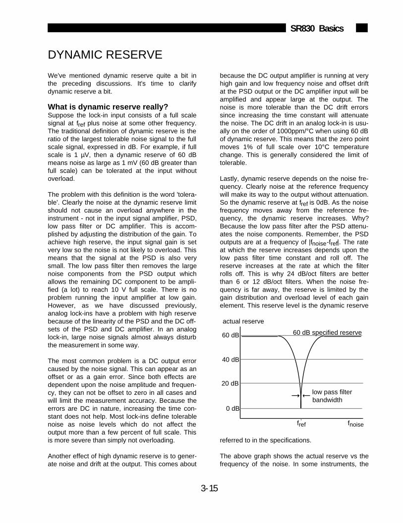
We've mentioned dynamic reserve quite a bit inthe preceding discussions. It's time to clarifydynamic reserve a bit.
What is dynamic reserve really?Suppose the lock-in input consists of a full scalesignal at fref plus noise at some other frequency.The traditional definition of dynamic reserve is theratio of the largest tolerable noise signal to the fullscale signal, expressed in dB. For example, if fullscale is 1 µV, then a dynamic reserve of 60 dBmeans noise as large as 1 mV (60 dB greater thanfull scale) can be tolerated at the input withoutoverload.
The problem with this definition is the word 'tolera-ble'. Clearly the noise at the dynamic reserve limitshould not cause an overload anywhere in theinstrument - not in the input signal amplifier, PSD,low pass filter or DC amplifier. This is accom-plished by adjusting the distribution of the gain. Toachieve high reserve, the input signal gain is setvery low so the noise is not likely to overload. Thismeans that the signal at the PSD is also verysmall. The low pass filter then removes the largenoise components from the PSD output whichallows the remaining DC component to be ampli-fied (a lot) to reach 10 V full scale. There is noproblem running the input amplifier at low gain.However, as we have discussed previously,analog lock-ins have a problem with high reservebecause of the linearity of the PSD and the DC off-sets of the PSD and DC amplifier. In an analoglock-in, large noise signals almost always disturbthe measurement in some way.
The most common problem is a DC output errorcaused by the noise signal. This can appear as anoffset or as a gain error. Since both effects aredependent upon the noise amplitude and frequen-cy, they can not be offset to zero in all cases andwill limit the measurement accuracy. Because theerrors are DC in nature, increasing the time con-stant does not help. Most lock-ins define tolerablenoise as noise levels which do not affect theoutput more than a few percent of full scale. Thisis more severe than simply not overloading.
Another effect of high dynamic reserve is to gener-ate noise and drift at the output. This comes about
because the DC output amplifier is running at veryhigh gain and low frequency noise and offset driftat the PSD output or the DC amplifier input will beamplified and appear large at the output. Thenoise is more tolerable than the DC drift errorssince increasing the time constant will attenuatethe noise. The DC drift in an analog lock-in is usu-ally on the order of 1000ppm/°C when using 60 dBof dynamic reserve. This means that the zero pointmoves 1% of full scale over 10°C temperaturechange. This is generally considered the limit oftolerable.
Lastly, dynamic reserve depends on the noise fre-quency. Clearly noise at the reference frequencywill make its way to the output without attenuation.So the dynamic reserve at fref is 0dB. As the noisefrequency moves away from the reference fre-quency, the dynamic reserve increases. Why?Because the low pass filter after the PSD attenu-ates the noise components. Remember, the PSDoutputs are at a frequency of |fnoise-fref|. The rateat which the reserve increases depends upon thelow pass filter time constant and roll off. Thereserve increases at the rate at which the filterrolls off. This is why 24 dB/oct filters are betterthan 6 or 12 dB/oct filters. When the noise fre-quency is far away, the reserve is limited by thegain distribution and overload level of each gainelement. This reserve level is the dynamic reserve
referred to in the specifications.
The above graph shows the actual reserve vs thefrequency of the noise. In some instruments, the
DYNAMIC RESERVE
fref
60 dB
40 dB
20 dB
0 dB
fnoise
actual reserve
low pass filter bandwidth
60 dB specified reserve
3-16
SR830 Basics
signal input attenuates frequencies far outside thelock-in's operating range (fnoise>>100 kHz). Inthese cases, the reserve can be higher at thesefrequencies than within the operating range. Whilethis may be a nice specification, removing noise atfrequencies very far from the reference does notrequire a lock-in amplifier. Lock-ins are used whenthere is noise at frequencies near the signal. Thus,the dynamic reserve for noise within the operatingrange is more important.
Dynamic reserve in the SR830The SR830, with its digital phase sensitive detec-tors, does not suffer from DC output errors causedby large noise signals. The dynamic reserve canbe increased to above 100 dB without measure-ment error. Large noise signals do not causeoutput errors from the PSD. The large DC gaindoes not result in increased output drift.
In fact, the only drawback to using ultra highdynamic reserves (>60 dB) is the increased outputnoise due to the noise of the A/D converter. Thisincrease in output noise is only present when thedynamic reserve is above 60 dB AND set to HighReserve or Normal. However, the Low Noisereserve can be very high as we'll see shortly.
To set a scale, the SR830's output noise at 100 dBdynamic reserve is only measurable when thesignal input is grounded. Let's do a simple experi-ment. If the lock-in reference is at 1 kHz and alarge signal is applied at 9.5 kHz, what will thelock-in output be? If the signal is increased to thedynamic reserve limit (100 dB greater than fullscale), the output will reflect the noise of the signalat 1 kHz. The spectrum of any pure sine generatoralways has a noise floor, i.e. there is some noiseat all frequencies. So even though the appliedsignal is at 9.5 kHz, there will be noise at all otherfrequencies, including the 1 kHz lock-in reference.This noise will be detected by the lock-in andappear as noise at the output. This output noisewill typically be greater than the SR830's ownoutput noise. In fact, virtually all signal sources willhave a noise floor which will dominate the lock-inoutput noise. Of course, noise signals are general-ly much noisier than pure sine generators and willhave much higher broadband noise floors.
If the noise does not reach the reserve limit, theSR830's own output noise may become detectableat ultra high reserves. In this case, simply lowerthe dynamic reserve and the DC gain will
decrease and the output noise will decrease also.In general, do not run with more reserve than nec-essary. Certainly don't use High Reserve whenthere is virtually no noise at all.
The frequency dependence of dynamic reserve isinherent in the lock-in detection technique. TheSR830, by providing more low pass filter stages,can increase the dynamic reserve close to the ref-erence frequency. The specified reserve applies tonoise signals within the operating range of thelock-in, i.e. frequencies below 100 kHz. Thereserve at higher frequencies is actually higher butis generally not that useful.
Minimum dynamic reserve (Low Noise)The SR830 always has a minimum amount ofdynamic reserve. This minimum reserve is the LowNoise reserve setting. The minimum reservechanges with the sensitivity (gain) of the instru-ment. At high gains (full scale sensitivity of 50 µVand below), the minimum dynamic reserveincreases from 37 dB at the same rate as the sen-sitivity increases. For example, the minimumreserve at 5 µV sensitivity is 57 dB. In manyanalog lock-ins, the reserve can be lower. Whycan't the SR830 run with lower reserve at thissensitivity?
The answer to this question is - Why would youwant lower reserve? In an analog lock-in, lowerreserve means less output error and drift. In theSR830, more reserve does not increase the outputerror or drift. More reserve can increase the outputnoise though. However, if the analog signal gainbefore the A/D converter is high enough, the5 nV/√Hz noise of the signal input will be amplifiedto a level greater than the input noise of the A/Dconverter. At this point, the detected noise willreflect the actual noise at the signal input and notthe A/D converter's noise. Increasing the analoggain (decreasing the reserve) will not decrease theoutput noise. Thus, there is no reason to decreasethe reserve. At a sensitivity of 5 µV, the analoggain is sufficiently high so that A/D converter noiseis not a problem. Sensitivities below 5 µV do notrequire any more gain since the signal to noiseratio will not be improved (the front end noise dom-inates). The SR830 does not increase the gainbelow the 5 µV sensitivity, instead, the minimumreserve increases. Of course, the input gain canbe decreased and the reserve increased, in whichcase the A/D converter noise might be detected inthe absence of any signal input.
3-17
SR830 Basics
A lock-in can measure signals as small as a fewnanovolts. A low noise signal amplifier is requiredto boost the signal to a level where the A/D con-verter can digitize the signal without degrading thesignal to noise. The analog gain in the SR830ranges from roughly 7 to 1000. As discussed pre-viously, higher gains do not improve signal tonoise and are not necessary.
The overall gain (AC plus DC) is determined bythe sensitivity. The distribution of the gain (ACversus DC) is set by the dynamic reserve.
Input noiseThe input noise of the SR830 signal amplifier isabout 5 nVrms/√Hz. What does this noise figuremean? Let's set up an experiment. If an amplifierhas 5 nVrms/√Hz of input noise and a gain of1000, then the output will have 5 µVrms/√Hz ofnoise. Suppose the amplifier output is low pass fil-tered with a single RC filter (6 dB/oct roll off) with atime constant of 100 ms. What will be the noise atthe filter output?
Amplifier input noise and Johnson noise of resis-tors are Gaussian in nature. That is, the amount ofnoise is proportional to the square root of thebandwidth in which the noise is measured. Asingle stage RC filter has an equivalent noisebandwidth (ENBW) of 1/4T where T is the timeconstant (RxC). This means that Gaussian noiseat the filter input is filtered with an effective band-width equal to the ENBW. In this example, thefilter sees 5 µVrms/√Hz of noise at its input. It hasan ENBW of 1/(4x100ms) or 2.5 Hz. The voltagenoise at the filter output will be5 µVrms/√Hz x √2.5Hz or 7.9 µVrms. For Gaussian noise, the peak to peak noise isabout 5 times the rms noise. Thus, the output willhave about 40 µV pk-pk of noise.
Input noise for a lock-in works the same way. Forsensitivities below about 5 µV full scale, the inputnoise will determine the output noise (at minimumreserve). The amount of noise at the output isdetermined by the ENBW of the low pass filter.See the discussion of noise later in this section formore information on ENBW. The ENBW dependsupon the time constant and filter roll off. For exam-ple, suppose the SR830 is set to 5 µV full scale
SIGNAL INPUT AMPLIFIER and FILTERS
with a 100 ms time constant and 6 dB/oct of filterroll off. The ENBW of a 100 ms, 6 dB/oct filter is2.5 Hz. The lock-in will measure the input noisewith an ENBW of 2.5 Hz. This translates to7.9 nVrms at the input. At the output, this repre-sents about 0.16% of full scale (7.9 nV/5 µV). Thepeak to peak noise will be about 0.8% of full scale.
All of this assumes that the signal input is beingdriven from a low impedance source. Rememberresistors have Johnson noise equal to0.13x√R nVrms/√Hz. Even a 50Ω resistor hasalmost 1 nVrms/√Hz of noise! A signal sourceimpedance of 2kΩ will have a Johnson noisegreater than the SR830's input noise. To deter-mine the overall noise of multiple noise sources,take the square root of the sum of the squares ofthe individual noise figures. For example, if a 2kΩsource impedance is used, the Johnson noise willbe 5.8 nVrms/√Hz. The overall noise at the SR830input will be [52 + 5.82]1/2 or 7.7 nVrms/√Hz.
We'll talk more about noise sources later in thissection.
At lower gains (sensitivities above 50 µV), there isnot enough gain at high reserve to amplify theinput noise to a level greater than the noise of theA/D converter. In these cases, the output noise isdetermined by the A/D noise. Fortunately, at thesesensitivities, the DC gain is low and the noise atthe output is negligible.
Notch filtersThe SR830 has two notch filters in the signalamplifier chain. These are pre-tuned to the line fre-quency (50 or 60 Hz) and twice the line frequency(100 or 120 Hz). In circumstances where the larg-est noise signals are at the power line frequencies,these filters can be engaged to remove noise sig-nals at these frequencies. Removing the largestnoise signals before the final gain stage canreduce the amount of dynamic reserve required toperform a measurement. To the extent that thesefilters reduce the required reserve to either 60 dBor the minimum reserve (whichever is higher), thensome improvement might be gained. If therequired reserve without these notch filters isbelow 60 dB or if the minimum reserve is suffi-cient, then these filters do not significantly improve
3-18
SR830 Basics
the measurement.
Using either of these filters precludes makingmeasurements in the vicinity of the notch frequen-cies. These filters have a finite range of attenua-tion, generally 10 Hz or so. Thus, if the lock-in ismaking measurements at 70 Hz, do not use the60 Hz notch filter! The signal will be attenuatedand the measurement will be in error. When meas-uring phase shifts, these filters can affect phasemeasurements up to an octave away.
Anti-aliasing filterAfter all of the signal filtering and amplification,there is an anti-aliasing filter. This filter is requiredby the signal digitization process. According to theNyquist criterion, signals must be sampled at a fre-quency at least twice the highest signal frequency.In this case, the highest signal frequency is100 kHz and the sampling frequency is 256 kHzso things are ok. However, no signals above 128kHz can be allowed to reach the A/D converter.These signals would violate the Nyquist criterionand be undersampled. The result of this under-sampling is to make these higher frequency sig-nals appear as lower frequencies in the digitaldata stream. Thus a signal at 175 kHz wouldappear below 100 kHz in the digital data streamand be detectable by the digital PSD. This wouldbe a problem.
To avoid this undersampling, the analog signal isfiltered to remove any signals above 154 kHz(when sampling at 256 kHz, signals above154 kHz will appear below 102 kHz). This filter hasa flat pass band from DC to 102 kHz so as not toaffect measurements in the operating range of thelock-in. The filter rolls off from 102 kHz to 154 kHzand achieves an attenuation above 154 kHz of atleast 100 dB. Amplitude variations and phaseshifts due to this filter are calibrated out at the fac-tory and do not affect measurements. This filter istransparent to the user.
Input ImpedanceThe input impedance of the SR830 is 10 MΩ. If ahigher input impedance is desired, then the SR550remote preamplifier must be used. The SR550 hasan input impedance of 100 MΩ and is AC coupledfrom 1 Hz to 100 kHz.
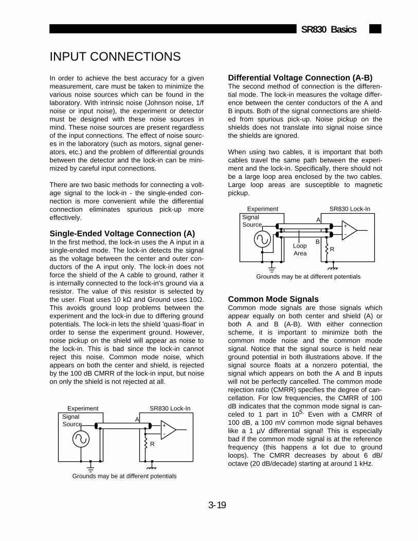
3-19
SR830 Basics
In order to achieve the best accuracy for a givenmeasurement, care must be taken to minimize thevarious noise sources which can be found in thelaboratory. With intrinsic noise (Johnson noise, 1/fnoise or input noise), the experiment or detectormust be designed with these noise sources inmind. These noise sources are present regardlessof the input connections. The effect of noise sourc-es in the laboratory (such as motors, signal gener-ators, etc.) and the problem of differential groundsbetween the detector and the lock-in can be mini-mized by careful input connections.
There are two basic methods for connecting a volt-age signal to the lock-in - the single-ended con-nection is more convenient while the differentialconnection eliminates spurious pick-up moreeffectively.
Single-Ended Voltage Connection (A)In the first method, the lock-in uses the A input in asingle-ended mode. The lock-in detects the signalas the voltage between the center and outer con-ductors of the A input only. The lock-in does notforce the shield of the A cable to ground, rather itis internally connected to the lock-in's ground via aresistor. The value of this resistor is selected bythe user. Float uses 10 kΩ and Ground uses 10Ω.This avoids ground loop problems between theexperiment and the lock-in due to differing groundpotentials. The lock-in lets the shield 'quasi-float' inorder to sense the experiment ground. However,noise pickup on the shield will appear as noise tothe lock-in. This is bad since the lock-in cannotreject this noise. Common mode noise, whichappears on both the center and shield, is rejectedby the 100 dB CMRR of the lock-in input, but noiseon only the shield is not rejected at all.
Differential Voltage Connection (A-B)The second method of connection is the differen-tial mode. The lock-in measures the voltage differ-ence between the center conductors of the A andB inputs. Both of the signal connections are shield-ed from spurious pick-up. Noise pickup on theshields does not translate into signal noise sincethe shields are ignored.
When using two cables, it is important that bothcables travel the same path between the experi-ment and the lock-in. Specifically, there should notbe a large loop area enclosed by the two cables.Large loop areas are susceptible to magneticpickup.
Common Mode SignalsCommon mode signals are those signals whichappear equally on both center and shield (A) orboth A and B (A-B). With either connectionscheme, it is important to minimize both thecommon mode noise and the common modesignal. Notice that the signal source is held nearground potential in both illustrations above. If thesignal source floats at a nonzero potential, thesignal which appears on both the A and B inputswill not be perfectly cancelled. The common moderejection ratio (CMRR) specifies the degree of can-cellation. For low frequencies, the CMRR of 100dB indicates that the common mode signal is can-celed to 1 part in 105. Even with a CMRR of100 dB, a 100 mV common mode signal behaveslike a 1 µV differential signal! This is especiallybad if the common mode signal is at the referencefrequency (this happens a lot due to groundloops). The CMRR decreases by about 6 dB/octave (20 dB/decade) starting at around 1 kHz.
INPUT CONNECTIONS
ExperimentSignal Source
R
SR830 Lock-In
A +-
Grounds may be at different potentials
BLoopArea
ExperimentSignal Source
R
SR830 Lock-In
A +-
Grounds may be at different potentials
3-20
SR830 Basics
Current Input (I)The current input on the SR830 uses the A inputBNC. The current input has a 1 kΩ input impe-dance and a current gain of either 106 or108 Volts/Amp. Currents from 1 µA down to 2 fAfull scale can be measured.
The impedance of the signal source is the mostimportant factor to consider in deciding betweenvoltage and current measurements.
For high source impedances, greater than 1 MΩ(106 gain) or 100 MΩ (108 gain), and small cur-rents, use the current input. Its relatively low impe-dance greatly reduces the amplitude and phaseerrors caused by the cable capacitance-sourceimpedance time constant. The cable capacitanceshould still be kept small to minimize the high fre-quency noise gain of the current preamplifier.
For moderate to low source impedances, or largercurrents, the voltage input is preferred. A smallvalue resistor may be used to shunt the signal cur-rent and generate a voltage signal. The lock-inthen measures the voltage across the shunt resis-tor. Select the resistor value to keep the shunt volt-age small (so it does not affect the source current)while providing enough signal for the lock-in tomeasure.
Which current gain should you use? The currentgain determines the input current noise of the lock-in as well as its measurement bandwidth. Signalsfar above the input bandwidth are attenuated by6 dB/oct. The noise and bandwidth are listedbelow.
Gain Noise Bandwidth
106 130 fA/√Hz 70 kHz108 13 fA/√Hz 700 Hz
AC vs DC CouplingThe signal input can be either AC or DC coupled.The AC coupling high pass filter passes signalsabove 160 mHz (0.16 Hz) and attenuates signalsat lower frequencies. AC coupling should be usedat frequencies above 160 mHz whenever possible.At lower frequencies, DC coupling is required.
A DC signal, if not removed by the AC couplingfilter, will multiply with the reference sine wave andproduce an output at the reference frequency. Thissignal is not normally present and needs to beremoved by the low pass filter. If the DC compo-nent of the signal is large, then this output will belarge and require a long time constant to remove.AC coupling removes the DC component of thesignal without any sacrifice in signal as long as thefrequency is above 160 mHz.
The current input current to voltage preamplifier isalways DC coupled. AC coupling can be selectedfollowing the current preamplifier to remove anyDC current signal.
3-21
SR830 Basics
Random noise finds its way into experiments in avariety of ways. Good experimental design canreduce these noise sources and improve themeasurement stability and accuracy.
There are a variety of intrinsic noise sources whichare present in all electronic signals. These sourcesare physical in origin.
Johnson noiseEvery resistor generates a noise voltage across itsterminals due to thermal fluctuations in the elec-tron density within the resistor itself. These fluctua-tions give rise to an open-circuit noise voltage,
where k=Boltzmann's constant (1.38x10⁻²³ J/°K),T is the temperature in °Kelvin (typically 300°K), Ris the resistance in Ohms, and ∆f is the bandwidthin Hz. ∆f is the bandwidth of the measurement.
Since the input signal amplifier in the SR830 has abandwidth of approximately 300 kHz, the effectivenoise at the amplifier input is Vnoise = 70√R nVrmsor 350√R nV pk-pk. This noise is broadband and ifthe source impedance of the signal is large, candetermine the amount of dynamic reserverequired.
The amount of noise measured by the lock-in isdetermined by the measurement bandwidth.Remember, the lock-in does not narrow its detec-tion bandwidth until after the phase sensitivedetectors. In a lock-in, the equivalent noise band-width (ENBW) of the low pass filter (time constant)sets the detection bandwidth. In this case, themeasured noise of a resistor at the lock-in input,typically the source impedance of the signal, issimply
The ENBW is determined by the time constant andslope as shown in the following table. Wait time isthe time required to reach 99% of its final value.
T= Time Constant
Slope ENBW Wait Time6 dB/oct 1/(4T) 5T12 dB/oct 1/(8T) 7T18 dB/oct 3/(32T) 9T24 dB/oct 5/(64T) 10T
The signal amplifier bandwidth determines theamount of broadband noise that will be amplified.This affects the dynamic reserve. The time con-stant sets the amount of noise which will be meas-ured at the reference frequency. See the SIGNALINPUT AMPLIFIER discussion for more informa-tion about Johnson noise.
Shot noiseElectric current has noise due to the finite natureof the charge carriers. There is always some non-uniformity in the electron flow which generatesnoise in the current. This noise is called shotnoise. This can appear as voltage noise when cur-rent is passed through a resistor, or as noise in acurrent measurement. The shot noise or currentnoise is given by
where q is the electron charge (1.6x10⁻¹⁹
Coulomb), I is the RMS AC current or DC currentdepending upon the circuit, and ∆f is thebandwidth.
When the current input of a lock-in is used tomeasure an AC signal current, the bandwidth istypically so small that shot noise is not important.
1/f noise Every 10 Ω resistor, no matter what it is made of,has the same Johnson noise. However, there isexcess noise in addition to Johnson noise whicharises from fluctuations in resistance due to thecurrent flowing through the resistor. For carboncomposition resistors, this is typically 0.1 µV-3 µVof rms noise per Volt of applied across the resis-tor. Metal film and wire-wound resistors haveabout 10 times less noise. This noise has a 1/fspectrum and makes measurements at low fre-quencies more difficult.
Other sources of 1/f noise include noise found in
INTRINSIC (RANDOM) NOISE SOURCES
Vnoise
(rms) = 4k TR∆ f( )1/2
Vnoise
(rms) = 0.13 R ENBW nV
Inoise
( rms) = 2q I∆ f( )1/2

3-22
SR830 Basics
quencies more difficult.
Other sources of 1/f noise include noise found invacuum tubes and semiconductors.
Total noiseAll of these noise sources are incoherent. Thetotal random noise is the square root of the sum ofthe squares of all the incoherent noise sources.
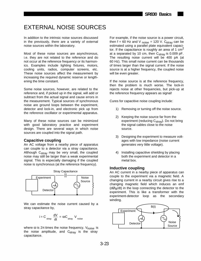
3-23
SR830 Basics
In addition to the intrinsic noise sources discussedin the previously, there are a variety of externalnoise sources within the laboratory.
Most of these noise sources are asynchronous,i.e. they are not related to the reference and donot occur at the reference frequency or its harmon-ics. Examples include lighting fixtures, motors,cooling units, radios, computer screens, etc.These noise sources affect the measurement byincreasing the required dynamic reserve or length-ening the time constant.
Some noise sources, however, are related to thereference and, if picked up in the signal, will add orsubtract from the actual signal and cause errors inthe measurement. Typical sources of synchronousnoise are ground loops between the experiment,detector and lock-in, and electronic pick up fromthe reference oscillator or experimental apparatus.
Many of these noise sources can be minimizedwith good laboratory practice and experimentdesign. There are several ways in which noisesources are coupled into the signal path.
Capacitive couplingAn AC voltage from a nearby piece of apparatuscan couple to a detector via a stray capacitance.Although Cstray may be very small, the couplednoise may still be larger than a weak experimentalsignal. This is especially damaging if the couplednoise is synchronous (at the reference frequency).
We can estimate the noise current caused by astray capacitance by,
where ω is 2π times the noise frequency, Vnoise isthe noise amplitude, and Cstray is the straycapacitance.
For example, if the noise source is a power circuit,then f = 60 Hz and V noise = 120 V. Cstray can beestimated using a parallel plate equivalent capaci-tor. If the capacitance is roughly an area of 1 cm2
at a separated by 10 cm, then Cstray is 0.009 pF.The resulting noise current will be 400 pA (at60 Hz). This small noise current can be thousandsof times larger than the signal current. If the noisesource is at a higher frequency, the coupled noisewill be even greater.
If the noise source is at the reference frequency,then the problem is much worse. The lock-inrejects noise at other frequencies, but pick-up atthe reference frequency appears as signal!
Cures for capacitive noise coupling include:
1) Removing or turning off the noise source.
2) Keeping the noise source far from theexperiment (reducing Cstray). Do not bringthe signal cables close to the noisesource.
3) Designing the experiment to measure volt-ages with low impedance (noise currentgenerates very little voltage).
4) Installing capacitive shielding by placingboth the experiment and detector in ametal box.
Inductive couplingAn AC current in a nearby piece of apparatus cancouple to the experiment via a magnetic field. Achanging current in a nearby circuit gives rise to achanging magnetic field which induces an emf(dØB/dt) in the loop connecting the detector to theexperiment. This is like a transformer with theexperiment-detector loop as the secondarywinding.
EXTERNAL NOISE SOURCES
i = Cstray
dVdt
= ωCstray
Vnoise
Detector
Stray Capacitance
Noise Source
Experiment
Detector Noise Source
ExperimentB(t)
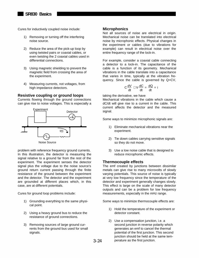
3-24
SR830 Basics
Cures for inductively coupled noise include:
1) Removing or turning off the interferingnoise source.
2) Reduce the area of the pick-up loop byusing twisted pairs or coaxial cables, oreven twisting the 2 coaxial cables used indifferential connections.
3) Using magnetic shielding to prevent themagnetic field from crossing the area ofthe experiment.
4) Measuring currents, not voltages, fromhigh impedance detectors.
Resistive coupling or ground loopsCurrents flowing through the ground connectionscan give rise to noise voltages. This is especially a
problem with reference frequency ground currents.In this illustration, the detector is measuring thesignal relative to a ground far from the rest of theexperiment. The experiment senses the detectorsignal plus the voltage due to the noise source'sground return current passing through the finiteresistance of the ground between the experimentand the detector. The detector and the experimentare grounded at different places which, in thiscase, are at different potentials.
Cures for ground loop problems include:
1) Grounding everything to the same physi-cal point.
2) Using a heavy ground bus to reduce theresistance of ground connections.
3) Removing sources of large ground cur-rents from the ground bus used for smallsignals.
Detector
Noise Source
Experiment
I(t)
MicrophonicsNot all sources of noise are electrical in origin.Mechanical noise can be translated into electricalnoise by microphonic effects. Physical changes inthe experiment or cables (due to vibrations forexample) can result in electrical noise over theentire frequency range of the lock-in.
For example, consider a coaxial cable connectinga detector to a lock-in. The capacitance of thecable is a function of its geometry. Mechanicalvibrations in the cable translate into a capacitancethat varies in time, typically at the vibration fre-quency. Since the cable is governed by Q=CV,
taking the derivative, we haveMechanical vibrations in the cable which cause adC/dt will give rise to a current in the cable. Thiscurrent affects the detector and the measuredsignal.
Some ways to minimize microphonic signals are:
1) Eliminate mechanical vibrations near theexperiment.
2) Tie down cables carrying sensitive signalsso they do not move.
3) Use a low noise cable that is designed toreduce microphonic effects.
Thermocouple effectsThe emf created by junctions between dissimilarmetals can give rise to many microvolts of slowlyvarying potentials. This source of noise is typicallyat very low frequency since the temperature of thedetector and experiment generally changes slowly.This effect is large on the scale of many detectoroutputs and can be a problem for low frequencymeasurements, especially in the mHz range.
Some ways to minimize thermocouple effects are:
1) Hold the temperature of the experiment ordetector constant.
2) Use a compensation junction, i.e. asecond junction in reverse polarity whichgenerates an emf to cancel the thermalpotential of the first junction. This secondjunction should be held at the same tem-perature as the first junction.
C dVdt
+ V dCdt
= dQdt
= i
3-25
SR830 Basics
Lock-in amplifiers can be used to measure noise.Noise measurements are generally used to char-acterize components and detectors.
The SR830 measures input signal noise AT thereference frequency. Many noise sources have afrequency dependence which the lock-in canmeasure.
How does a lock-in measure noise?Remember that the lock-in detects signals close tothe reference frequency. How close? Input signalswithin the detection bandwidth set by the low passfilter time constant and roll-off appear at the outputat a frequency f=fsig-fref. Input noise near frefappears as noise at the output with a bandwidth ofDC to the detection bandwidth.
For Gaussian noise, the equivalent noise band-width (ENBW) of a low pass filter is the bandwidthof the perfect rectangular filter which passes thesame amount of noise as the real filter.
The ENBW is determined by the time constant andslope as shown below. Wait time is the timerequired to reach 99% of its final value.
T= Time Constant
Slope ENBW Wait Time6 dB/oct 1/(4T) 5T12 dB/oct 1/(8T) 7T18 dB/oct 3/(32T) 9T24 dB/oct 5/(64T) 10T
Noise estimationThe noise is simply the standard deviation (root ofthe mean of the squared deviations)of the meas-ured X, Y or R .
The above technique, while mathematically sound,can not provide a real time output or an analogoutput proportional to the measured noise. Forthese measurements, the SR830 estimates the Xor Y noise directly.
To display the noise of X, for example, simply setthe CH1 display to X noise. The quantity X noise iscomputed from the measured values of X usingthe following algorithm. The moving average of X
NOISE MEASUREMENTS
is computed. This is the mean value of X oversome past history. The present mean value of X issubtracted from the present value of X to find thedeviation of X from the mean. Finally, the movingaverage of the absolute value of the deviations iscalculated. This calculation is called the meanaverage deviation or MAD. This is not the same asan RMS calculation. However, if the noise isGaussian in nature, then the RMS noise and theMAD noise are related by a constant factor.
The SR830 uses the MAD method to estimate theRMS noise of X and Y. The advantage of this tech-nique is its numerical simplicity and speed.
The noise calculations for X and Y occur at512 Hz. At each sample, the mean and movingaverage of the absolute value of the deviations iscalculated. The averaging time (for the mean andaverage deviation) depends upon the time con-stant. The averaging time is selected by theSR830 and ranges from 10 to 80 times the timeconstant. Shorter averaging times yield a verypoor estimate of the noise (the mean varies rapidlyand the deviations are not averaged well). Longeraveraging times, while yielding better results, takea long time to settle to a steady answer.
To change the settling time, change the time con-stant. Remember, shorter settling times use small-er time constants (higher noise bandwidths) andyield noisier noise estimates.
X and Y noise are displayed in units ofVolts/√Hz. The ENBW of the time constant isalready factored into the calculation. Thus, themean displayed value of the noise should notdepend upon the time constant.
The SR830 performs the noise calculations all ofthe time, whether or not X or Y noise are beingdisplayed. Thus, as soon as X noise is displayed,the value shown is up to date and no settling timeis required. If the sensitivity is changed, then thenoise estimate will need to settle to the correctvalue.

3-26
SR830 Basics
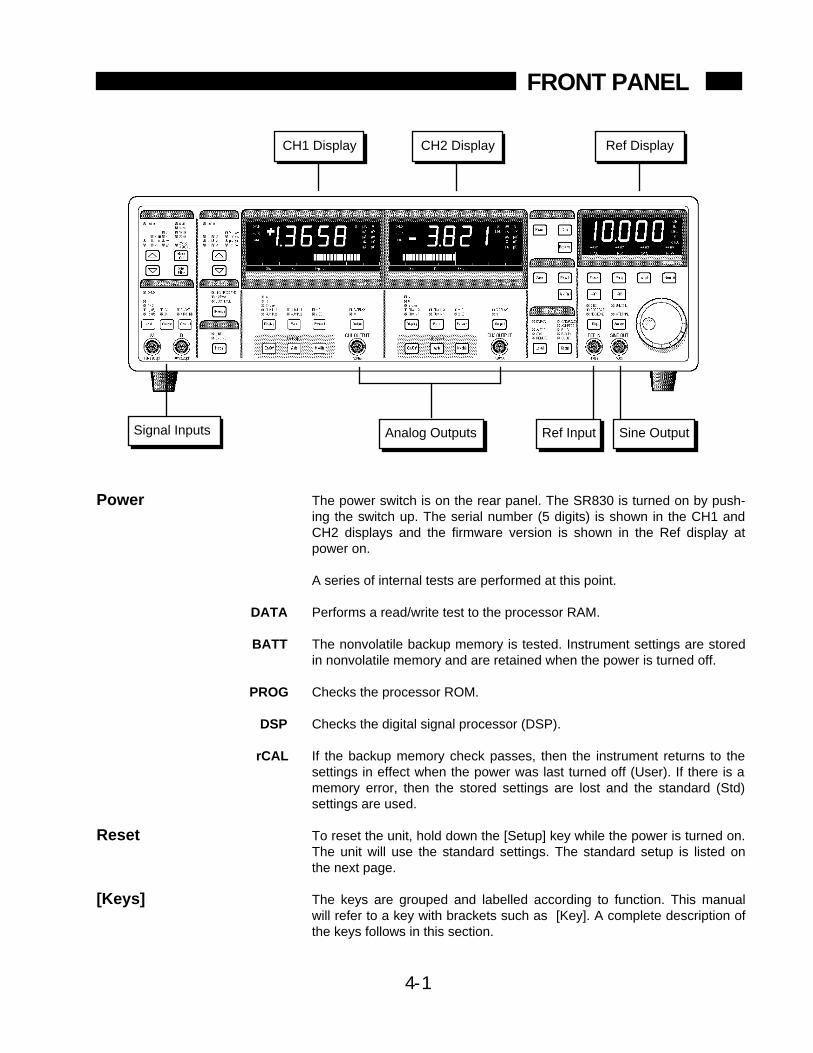
4-1
Analog Outputs
CH1 Display
Power The power switch is on the rear panel. The SR830 is turned on by push-ing the switch up. The serial number (5 digits) is shown in the CH1 andCH2 displays and the firmware version is shown in the Ref display atpower on.
A series of internal tests are performed at this point.
DATA Performs a read/write test to the processor RAM.
BATT The nonvolatile backup memory is tested. Instrument settings are storedin nonvolatile memory and are retained when the power is turned off.
PROG Checks the processor ROM.
DSP Checks the digital signal processor (DSP).
rCAL If the backup memory check passes, then the instrument returns to thesettings in effect when the power was last turned off (User). If there is amemory error, then the stored settings are lost and the standard (Std)settings are used.
Reset To reset the unit, hold down the [Setup] key while the power is turned on.The unit will use the standard settings. The standard setup is listed onthe next page.
[Keys] The keys are grouped and labelled according to function. This manualwill refer to a key with brackets such as [Key]. A complete description ofthe keys follows in this section.
Signal Inputs
FRONT PANEL
CH2 Display Ref Display
Ref Input Sine Output
4-2
Front Panel
Knob The knob is used to adjust parameters in the Reference display. Theparameters which may be adjusted are internal reference frequency, ref-erence phase shift, sine output amplitude, harmonic detect number, off-sets, Aux Output levels, and various Setup parameters.
Local Lockout If the computer interface has placed the unit in the REMOTE state, indi-cated by the REMOTE led, then the keys and the knob are disabled.Attempts to change the settings from the front panel will display the mes-sage 'LOCL LOut' indicating local control is locked out by the interface.
Reference Input The reference input can be a sine wave (rising zero crossing detected) ora TTL pulse or square wave (rising or falling edge). The input impedanceis 1 MΩ AC coupled (>1 Hz) for the sine input. For low frequencies (<1Hz), it is necessary to use a TTL reference signal. The TTL input pro-vides the best overall performance and should be used whenever possi-ble.
Sine Out The internal oscillator output has a 50Ω output impedance and varies inamplitude from 4 mVrms to 5 Vrms. The output level is specified into ahigh impedance load. If the output is terminated in a low impedance,such as 50Ω, the amplitude will be less than the programmed amplitude(half for a 50Ω load).
This output is active even when an external reference is used. In thiscase, the sine wave is phase locked to the reference and its amplitude isprogrammable.
A TTL sync output is provided on the rear panel. This output is useful fortriggering scopes and other equipment at the reference frequency. TheTTL sync output is a square wave derived from the zero crossings of thesine output.
CH1 & CH2 Outputs The Channel 1 and Channel 2 outputs can be configured to output a volt-age from -10 V to +10 V proportional to X or Y or the CH1 and CH2Displays. ±10 V is full scale. The outputs can source 10 mA maximum.
Signal Inputs The input mode may be single-ended, A, or differential, A-B. The A and Binputs are voltage inputs with 10 MΩ, 25 pF input impedance. Their con-nector shields are isolated from the chassis by 10 Ω (Ground) or 1 kΩ(Float). Do not apply more than 50 V to either input. The shields shouldnever exceed 1 V. The I (current) input is 1 kΩ to a virtual ground.
Key Click On/Off Press the [Phase] and [Harm#] keys together to toggle the key click onand off.
Front Panel Display Test To test the front panel displays, press the [Phase] and [Freq] keystogether. All of the LED's will turn on. Press [Phase] to decrease thenumber of on LED's to half on, a single LED and no LED's on. Use theknob to move the turned on LED's across the panel. Press [Freq] toincrease the number of on LED's. Make sure that every LED can beturned on. Press any other key to exit this test mode.
Display Off Operation To operate with the front panel displays off, press [Phase] and [Freq]
4-3
Front Panel
together to enter the front panel test mode. Press [Phase] to decreasethe number of on LED's until all of the LED's are off. The SR830 is stilloperating, the output voltages are updated and the unit responds to inter-face commands. To change a setting, press any key other than [Phase]or [Freq] to return to normal operation, change the desired parameter,then press [Phase] and [Freq] together to return to the test mode. Turnthe LED's all off with the [Phase] key.
Keypad Test To test the keypad, press the [Phase] and [Ampl] keys together. TheCH1 and CH2 displays will read 'PAd codE' and a number of LED indica-tors will be turned on. The LED's indicate which keys have not beenpressed yet. Press all of the keys on the front panel, one at a time. Aseach key is pressed, the key code is displayed in the Reference display,and the nearest indicator LED turns off. When all of the keys have beenpressed, the display will return to normal. To return to normal operationwithout pressing all of the keys, simply turn the knob.
4-4
Front Panel
REFERENCE / PHASEPhase 0.000°Reference Source InternalHarmonic # 1Sine Amplitude 1.000 VrmsInternal Frequency 1.000 kHzExt Reference Trigger Sine
INPUT / FILTERSSource AGrounding FloatCoupling ACLine Notches Out
GAIN / TCSensitivity 1 VReserve Low NoiseTime Constant 100 msFilter dB/oct. 12 dBSynchronous Off
DISPLAY CH1 XCH2 YRatio NoneReference Frequency
STANDARD SETTINGS
If the [Setup] key is held down when the power is turned on, the lock-in settings will be set to the defaultsshown below rather than the settings that were in effect when the power was last turned off. The default set-tings may also be recalled using the RST command over the computer interface. In this case, the communi-cations parameters and status registers are not changed.
OUTPUT / OFFSETCH1 Output XCH2 Output YAll Offsets 0.00%All Expands 1
AUX OUTPUTSAll Output Voltages 0.000 V
SETUPOutput To GPIBGPIB Address 8RS232 Baud Rate 9600Parity NoneKey Click OnAlarms OnOverride Remote On
DATA STORAGESample Rate 1 HzScan Mode LoopTrigger Starts No
STATUS ENABLEREGISTERS Cleared
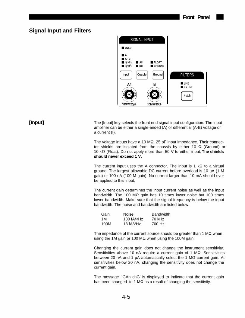
4-5
Front Panel
Signal Input and Filters
[Input] The [Input] key selects the front end signal input configuration. The inputamplifier can be either a single-ended (A) or differential (A-B) voltage ora current (I).
The voltage inputs have a 10 MΩ, 25 pF input impedance. Their connec-tor shields are isolated from the chassis by either 10 Ω (Ground) or10 kΩ (Float). Do not apply more than 50 V to either input. The shieldsshould never exceed 1 V.
The current input uses the A connector. The input is 1 kΩ to a virtualground. The largest allowable DC current before overload is 10 µA (1 Mgain) or 100 nA (100 M gain). No current larger than 10 mA should everbe applied to this input.
The current gain determines the input current noise as well as the inputbandwidth. The 100 MΩ gain has 10 times lower noise but 100 timeslower bandwidth. Make sure that the signal frequency is below the inputbandwidth. The noise and bandwidth are listed below.
Gain Noise Bandwidth1M 130 fA/√Hz 70 kHz100M 13 fA/√Hz 700 Hz
The impedance of the current source should be greater than 1 MΩ whenusing the 1M gain or 100 MΩ when using the 100M gain.
Changing the current gain does not change the instrument sensitivity.Sensitivities above 10 nA require a current gain of 1 MΩ. Sensitivitiesbetween 20 nA and 1 µA automatically select the 1 MΩ current gain. Atsensitivities below 20 nA, changing the sensitivity does not change thecurrent gain.
The message 'IGAn chG' is displayed to indicate that the current gainhas been changed to 1 MΩ as a result of changing the sensitivity.
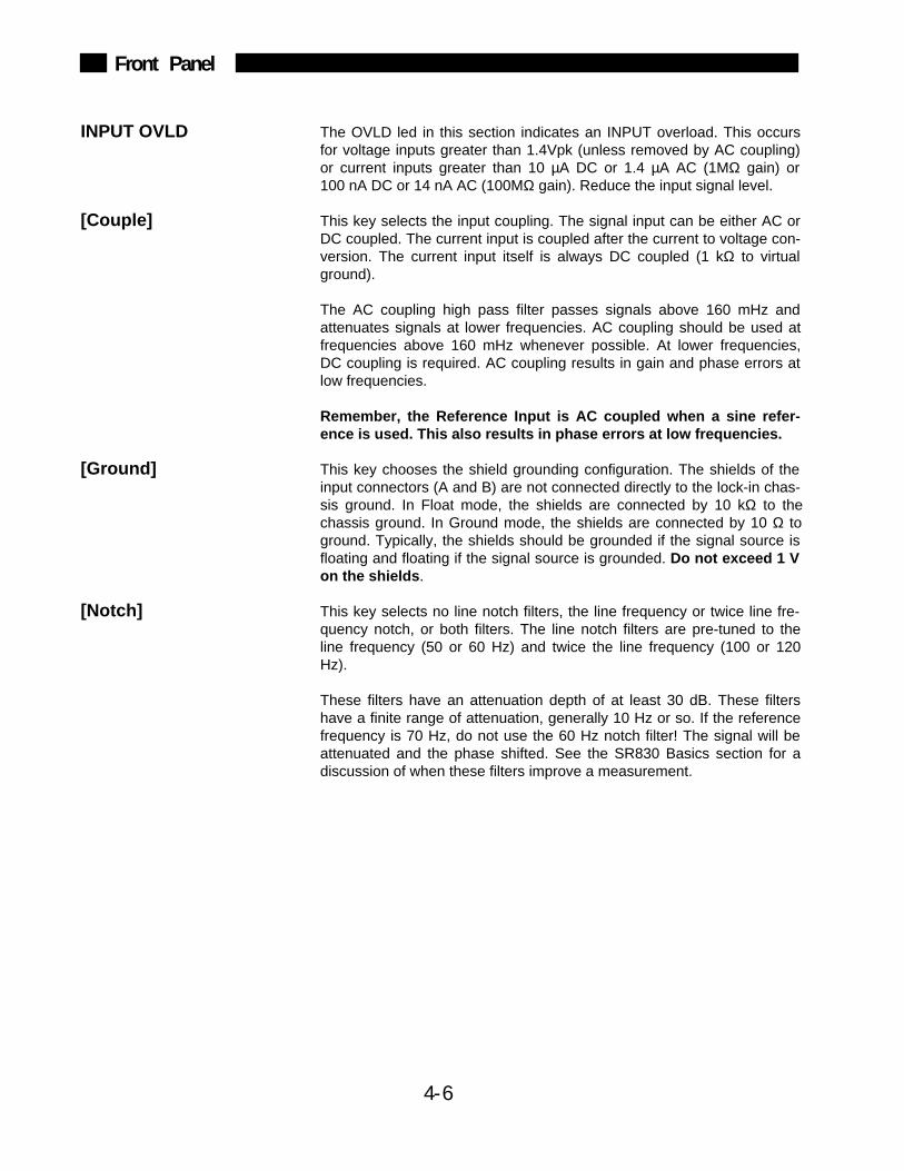
4-6
Front Panel
INPUT OVLD The OVLD led in this section indicates an INPUT overload. This occursfor voltage inputs greater than 1.4Vpk (unless removed by AC coupling)or current inputs greater than 10 µA DC or 1.4 µA AC (1MΩ gain) or100 nA DC or 14 nA AC (100MΩ gain). Reduce the input signal level.
[Couple] This key selects the input coupling. The signal input can be either AC orDC coupled. The current input is coupled after the current to voltage con-version. The current input itself is always DC coupled (1 kΩ to virtualground).
The AC coupling high pass filter passes signals above 160 mHz andattenuates signals at lower frequencies. AC coupling should be used atfrequencies above 160 mHz whenever possible. At lower frequencies,DC coupling is required. AC coupling results in gain and phase errors atlow frequencies.
Remember, the Reference Input is AC coupled when a sine refer-ence is used. This also results in phase errors at low frequencies.
[Ground] This key chooses the shield grounding configuration. The shields of theinput connectors (A and B) are not connected directly to the lock-in chas-sis ground. In Float mode, the shields are connected by 10 kΩ to thechassis ground. In Ground mode, the shields are connected by 10 Ω toground. Typically, the shields should be grounded if the signal source isfloating and floating if the signal source is grounded. Do not exceed 1 Von the shields.
[Notch] This key selects no line notch filters, the line frequency or twice line fre-quency notch, or both filters. The line notch filters are pre-tuned to theline frequency (50 or 60 Hz) and twice the line frequency (100 or 120Hz).
These filters have an attenuation depth of at least 30 dB. These filtershave a finite range of attenuation, generally 10 Hz or so. If the referencefrequency is 70 Hz, do not use the 60 Hz notch filter! The signal will beattenuated and the phase shifted. See the SR830 Basics section for adiscussion of when these filters improve a measurement.
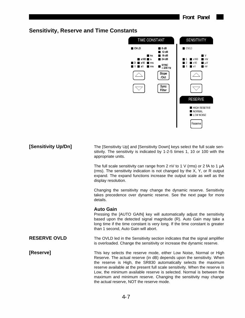
4-7
Front Panel
Sensitivity, Reserve and Time Constants
[Sensitivity Up/Dn] The [Sensitivity Up] and [Sensitivity Down] keys select the full scale sen-sitivity. The sensitivity is indicated by 1-2-5 times 1, 10 or 100 with theappropriate units.
The full scale sensitivity can range from 2 nV to 1 V (rms) or 2 fA to 1 µA(rms). The sensitivity indication is not changed by the X, Y, or R outputexpand. The expand functions increase the output scale as well as thedisplay resolution.
Changing the sensitivity may change the dynamic reserve. Sensitivitytakes precedence over dynamic reserve. See the next page for moredetails.
Auto GainPressing the [AUTO GAIN] key will automatically adjust the sensitivitybased upon the detected signal magnitude (R). Auto Gain may take along time if the time constant is very long. If the time constant is greaterthan 1 second, Auto Gain will abort.
RESERVE OVLD The OVLD led in the Sensitivity section indicates that the signal amplifieris overloaded. Change the sensitivity or increase the dynamic reserve.
[Reserve] This key selects the reserve mode, either Low Noise, Normal or HighReserve. The actual reserve (in dB) depends upon the sensitivity. Whenthe reserve is High, the SR830 automatically selects the maximumreserve available at the present full scale sensitivity. When the reserve isLow, the minimum available reserve is selected. Normal is between themaximum and minimum reserve. Changing the sensitivity may changethe actual reserve, NOT the reserve mode.
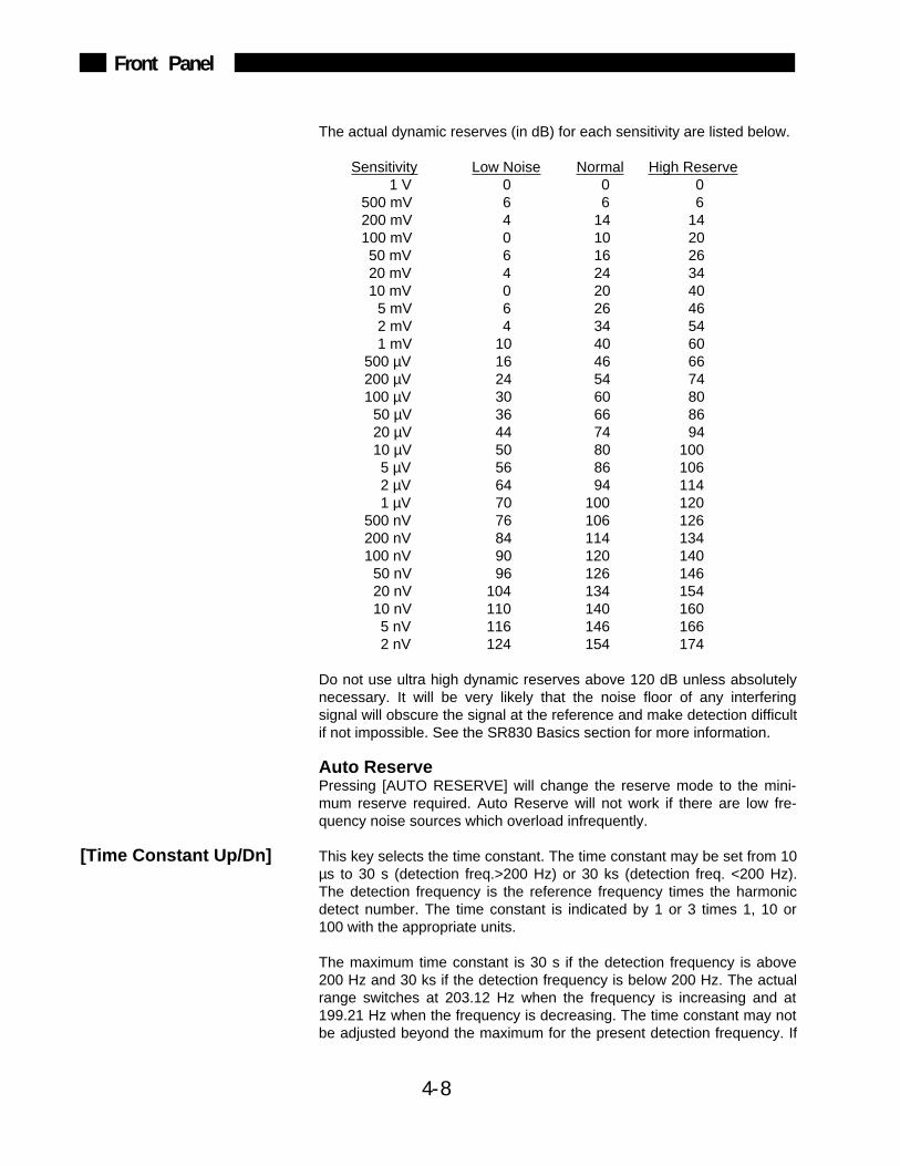
4-8
Front Panel
The actual dynamic reserves (in dB) for each sensitivity are listed below.
Sensitivity Low Noise Normal High Reserve1 V 0 0 0
500 mV 6 6 6200 mV 4 14 14100 mV 0 10 2050 mV 6 16 2620 mV 4 24 3410 mV 0 20 40
5 mV 6 26 462 mV 4 34 541 mV 10 40 60
500 µV 16 46 66200 µV 24 54 74100 µV 30 60 80
50 µV 36 66 8620 µV 44 74 9410 µV 50 80 1005 µV 56 86 1062 µV 64 94 1141 µV 70 100 120
500 nV 76 106 126200 nV 84 114 134100 nV 90 120 140
50 nV 96 126 14620 nV 104 134 15410 nV 110 140 1605 nV 116 146 1662 nV 124 154 174
Do not use ultra high dynamic reserves above 120 dB unless absolutelynecessary. It will be very likely that the noise floor of any interferingsignal will obscure the signal at the reference and make detection difficultif not impossible. See the SR830 Basics section for more information.
Auto ReservePressing [AUTO RESERVE] will change the reserve mode to the mini-mum reserve required. Auto Reserve will not work if there are low fre-quency noise sources which overload infrequently.
[Time Constant Up/Dn] This key selects the time constant. The time constant may be set from 10µs to 30 s (detection freq.>200 Hz) or 30 ks (detection freq. <200 Hz).The detection frequency is the reference frequency times the harmonicdetect number. The time constant is indicated by 1 or 3 times 1, 10 or100 with the appropriate units.
The maximum time constant is 30 s if the detection frequency is above200 Hz and 30 ks if the detection frequency is below 200 Hz. The actualrange switches at 203.12 Hz when the frequency is increasing and at199.21 Hz when the frequency is decreasing. The time constant may notbe adjusted beyond the maximum for the present detection frequency. If
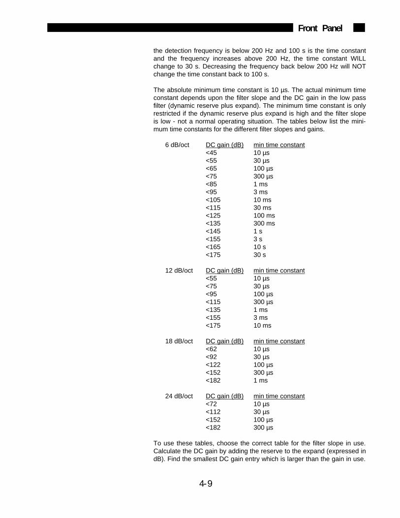
4-9
Front Panel
the detection frequency is below 200 Hz and 100 s is the time constantand the frequency increases above 200 Hz, the time constant WILLchange to 30 s. Decreasing the frequency back below 200 Hz will NOTchange the time constant back to 100 s.
The absolute minimum time constant is 10 µs. The actual minimum timeconstant depends upon the filter slope and the DC gain in the low passfilter (dynamic reserve plus expand). The minimum time constant is onlyrestricted if the dynamic reserve plus expand is high and the filter slopeis low - not a normal operating situation. The tables below list the mini-mum time constants for the different filter slopes and gains.
6 dB/oct DC gain (dB) min time constant<45 10 µs<55 30 µs<65 100 µs<75 300 µs<85 1 ms<95 3 ms<105 10 ms<115 30 ms<125 100 ms<135 300 ms<145 1 s<155 3 s<165 10 s<175 30 s
12 dB/oct DC gain (dB) min time constant<55 10 µs<75 30 µs<95 100 µs<115 300 µs<135 1 ms<155 3 ms<175 10 ms
18 dB/oct DC gain (dB) min time constant<62 10 µs<92 30 µs<122 100 µs<152 300 µs<182 1 ms
24 dB/oct DC gain (dB) min time constant<72 10 µs<112 30 µs<152 100 µs<182 300 µs
To use these tables, choose the correct table for the filter slope in use.Calculate the DC gain by adding the reserve to the expand (expressed indB). Find the smallest DC gain entry which is larger than the gain in use.
4-10
Front Panel
Read the minimum time constant for this entry. For example, if the slopeis 12 dB/oct, the reserve is 64 dB, and the X expand is 10 (20 dB), thenthe DC gain is 84 dB and the min time constant is 100 µs.
Time constant is a low priority parameter. If the sensitivity, dynamicreserve, filter slope, or expand is changed, and the present time constantis below the new minimum, the time constant WILL change to the newminimum. Remember, changing the sensitivity may change the reserveand thus change the time constant.
The message 'tc chnG' will be displayed to indicate that the time constanthas been changed, either by increasing the detection frequency above200 Hz, or by changing the sensitivity, dynamic reserve, filter slope, orexpand.
The time constant also determines the equivalent noise bandwidth(ENBW) of the low pass filter. This is the measurement bandwidth for Xand Y noise and depends upon the time constant and filter slope. (Seethe Noise discussion in the SR830 Basics section.)
FILTER OVLD The OVLD led in the Time Constant section indicates that the low passfilters have overloaded. Increase the time constant or filter roll-off, ordecrease the dynamic reserve.
Analog Outputs with Short Time ConstantsWhen using short time constants below 10 ms, the X and Y analog out-puts from the rear panel or the CH1 and CH2 outputs configured tooutput X or Y should be used. These outputs have a 100 kHz bandwidthand are accurate even with short time constants. CH1 or CH2 outputsproportional to the Displays (even if X or Y is displayed) are updated at a512 Hz rate. These outputs do not accurately reflect high frequency out-puts.
[Slope /oct] This key selects the low pass filter slope (number of poles). Each polecontributes 6 dB/oct of roll off. Using a higher slope can decrease therequired time constant and make a measurement faster. The filter slopeaffects the minimum time constant (see above). Changing the slope maychange the time constant if the present time constant is shorter than theminimum time constant at the new filter slope.
[Sync Filter] Pressing this key selects no synchronous filtering or synchronous filteringon below 200 Hz. In the second case, the synchronous filter is switchedon whenever the detection frequency decreases below 199.21 Hz andswitched off when the detection frequency increases above 203.12 Hz.The detection frequency is the reference frequency times the harmonicdetect number. The SYNC indicator in the CH1 display is turned onwhenever synchronous filtering is active.
When the synchronous filter is on, the phase sensitive detectors (PSD's)are followed by 2 poles of low pass filtering, the synchronous filter, then 2more poles of low pass filtering. The low pass filters are set by the timeconstant and filter slope. If the filter slope requires less then 4 poles(<24 dB/oct), then the unused poles are set to a minimum time constant.
4-11
Front Panel
The poles which are set by the time constant are the ones closest to thePSD's. For example, if the time constant is 100 ms with 12 dB/oct slopeand synchronous filtering is on, then the PSD's are followed by two polesof low pass filtering with 100 ms time constant, the synchronous filter,then two poles of minimum time constant.
Synchronous filtering removes outputs at harmonics of the reference fre-quency, most commonly 2xf. This is very effective at low reference fre-quencies since 2xf outputs would require very long time constants toremove. The synchronous filter does NOT attenuate broadband noise(except at the harmonic frequencies). The low pass filters remove out-puts due to noise and interfering signals. See the SR830 Basics sectionfor a discussion of time constants and filtering.
Note:The synchronous filter averages the outputs over a complete period.Each period is divided into 128 equal time slots. At each slot, the aver-age over the previous 128 slots is computed and output. This results inan output rate of 128xf. This output is then smoothed by the two poles offiltering which follow the synchronous filter.
The settling time of the synchronous filter is one period of the detectionfrequency. If the amplitude, frequency, phase, time constant or slope ischanged, then the outputs will settle for one period. These transients arebecause the synchronous filter provides a steady output only if the inputis repetitive from period to period. The transient response also dependsupon the time constants of the regular filters. Very short time constants(<<period) have little effect on the transient response. Longer time con-stants (<period) can magnify the amplitude of a transient. Much longertime constants (≥ period) will increase the settling time far beyond aperiod.
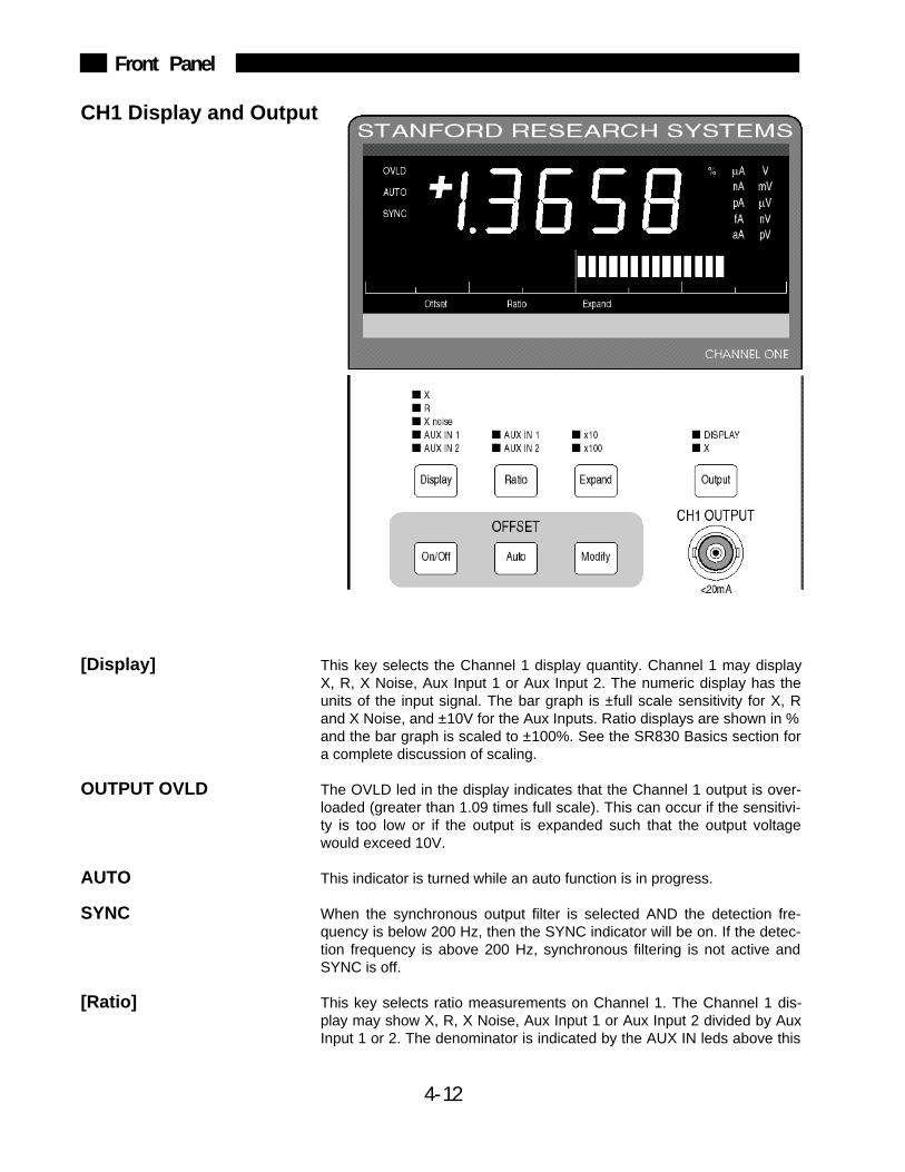
4-12
Front Panel
CH1 Display and Output
[Display] This key selects the Channel 1 display quantity. Channel 1 may displayX, R, X Noise, Aux Input 1 or Aux Input 2. The numeric display has theunits of the input signal. The bar graph is ±full scale sensitivity for X, Rand X Noise, and ±10V for the Aux Inputs. Ratio displays are shown in %and the bar graph is scaled to ±100%. See the SR830 Basics section fora complete discussion of scaling.
OUTPUT OVLD The OVLD led in the display indicates that the Channel 1 output is over-loaded (greater than 1.09 times full scale). This can occur if the sensitivi-ty is too low or if the output is expanded such that the output voltagewould exceed 10V.
AUTO This indicator is turned while an auto function is in progress.
SYNC When the synchronous output filter is selected AND the detection fre-quency is below 200 Hz, then the SYNC indicator will be on. If the detec-tion frequency is above 200 Hz, synchronous filtering is not active andSYNC is off.
[Ratio] This key selects ratio measurements on Channel 1. The Channel 1 dis-play may show X, R, X Noise, Aux Input 1 or Aux Input 2 divided by AuxInput 1 or 2. The denominator is indicated by the AUX IN leds above this
4-13
Front Panel
key. The Ratio indicator in the display is on to indicate a ratio measure-ment. Pressing this key until the AUX IN leds and the Ratio indicator areoff returns the measurement to non-ratio mode.
[Output] This key selects the CH1 OUTPUT source. The Channel 1 Output canprovide an analog output proportional to the Display or X. The output pro-portional to X has a bandwidth of 100 kHz (the output is updated at 256kHz). This output is the traditional X output of a lock-in. Output propor-tional to the display (even if the display is simply X) has a bandwidth of200 Hz (updated at 512 Hz).
Remember, The X output has 100 kHz of bandwidth. The Display outputshould only be used if the time constant is sufficiently long such thatthere are no high frequency outputs.
CH1 Offset and Expand The X and R outputs may be offset and expanded separately. Chooseeither X or R with the [Display] key to adjust the X or R offset andexpand.
X and R analog outputs are determined by
Output = (signal/sensitivity - offset) x Expand x 10 V
The output is normally 10 V for a full scale signal. The offset subtracts apercentage of full scale from the output. Expand multiplies the remainderby a factor from 1, 10 or 100.
Output offsets ARE reflected in displays which depend upon X or R.
X and Y offsets do NOT affect the calculation of R and θ.
Output expands do NOT increase the displayed values of X or R. Expandincreases the display resolution.
If the display is showing a quantity which is affected by an offset or anon-unity expand, then the Offset and Expand indicators are turned onbelow the display.
See the SR830 Basics section for a complete discussion of scaling, off-sets and expands.
[Offset On/Off] Pressing this key turns the X or R offset (as selected by the [Display]key) on or off. The Offset indicator below the display turns on when thedisplayed quantity is offset. This key allows the offset to be turned on andoff without adjusting the actual offset percentage.
[Modify] This key displays the X or R offset percentage (as selected by the[Display] key) in the Reference Display. Use the knob to adjust the offset.The Channel 1 display reflects the offset as it is adjusted while theReference display shows the actual offset percentage. The offset rangesfrom -105.00% to 105.00% of full scale. The offset percentage doesnot change with sensitivity - it is an output function. To return theReference Display to its original display, press the desired reference
4-14
Front Panel
display key ([Phase], [Freq], [Ampl], [Harm #] or [Aux Out]).
[Auto Offset] Pressing this key automatically sets the X or R offset percentage to offsetthe selected output quantity to zero.
[Expand] Pressing this key selects the X and R Expand. Use the [Display] key toselect either X or R. The expand can be 1 (no expand), 10 or 100. If theexpand is 10 or 100, the Expand indicator below the display will turn on.The output can never exceed full scale when expanded. For example, ifan output is 10% of full scale, the largest expand (with no offset) whichdoes not overload is 10. An output expanded beyond full scale will beoverloaded.
Short Time Constant LimitationsA short time constant places a limit on the total amount of DC gain(reserve plus expand) available. If the time constant is short, the filterslope low and the dynamic reserve high, then increasing the expand maychange the time constant. See the table of time constants and DC gainsin the Gain and Time Constant section.
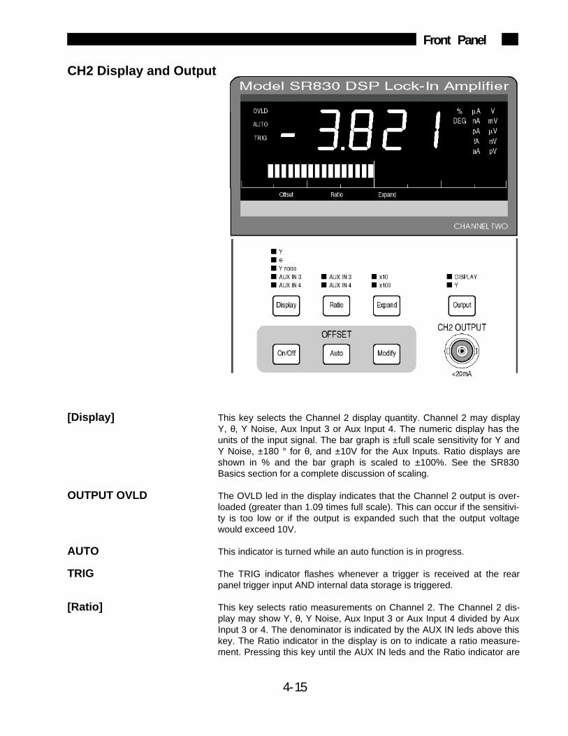
4-15
Front Panel
CH2 Display and Output
[Display] This key selects the Channel 2 display quantity. Channel 2 may displayY, θ, Y Noise, Aux Input 3 or Aux Input 4. The numeric display has theunits of the input signal. The bar graph is ±full scale sensitivity for Y andY Noise, ±180 ° for θ, and ±10V for the Aux Inputs. Ratio displays areshown in % and the bar graph is scaled to ±100%. See the SR830Basics section for a complete discussion of scaling.
OUTPUT OVLD The OVLD led in the display indicates that the Channel 2 output is over-loaded (greater than 1.09 times full scale). This can occur if the sensitivi-ty is too low or if the output is expanded such that the output voltagewould exceed 10V.
AUTO This indicator is turned while an auto function is in progress.
TRIG The TRIG indicator flashes whenever a trigger is received at the rearpanel trigger input AND internal data storage is triggered.
[Ratio] This key selects ratio measurements on Channel 2. The Channel 2 dis-play may show Y, θ, Y Noise, Aux Input 3 or Aux Input 4 divided by AuxInput 3 or 4. The denominator is indicated by the AUX IN leds above thiskey. The Ratio indicator in the display is on to indicate a ratio measure-ment. Pressing this key until the AUX IN leds and the Ratio indicator are
4-16
Front Panel
off returns the measurement to non-ratio mode.[Output] This key selects the CH2 OUTPUT source. The Channel 2 Output can
provide an analog output proportional to the Display or Y. The output pro-portional to Y has a bandwidth of 100 kHz (the output is updated at 256kHz). This output is the traditional Y output of a lock-in. Output propor-tional to the display (even if the display is simply Y) has a bandwidth of200 Hz (updated at 512 Hz).
Remember, The Y output has 100 kHz of bandwidth. The Display outputshould only be used if the time constant is sufficiently long such thatthere are no high frequency outputs.
CH2 Offset and Expand The Y output may be offset and expanded. Choose Y with the [Display]key to adjust the Y offset and expand.
The Y analog output is determined by
Output = (signal/sensitivity - offset) x Expand x 10 V
The output is normally 10 V for a full scale signal. The offset subtracts apercentage of full scale from the output. Expand multiplies the remainderby a factor from 1, 10 or 100.
Y Output offset IS reflected in displays which depend upon Y.
X and Y offsets do NOT affect the calculation of R or θ.
Y Output expand does NOT increase the displayed value Y. Expandincreases the display resolution.
If the display is showing a quantity which is affected by an offset or anon-unity expand, then the Offset and Expand indicators are turned onbelow the display.
See the SR830 Basics section for a complete discussion of scaling, off-sets and expands.
[Offset On/Off] Pressing this key turns the Y offset on or off. The Offset indicator belowthe display turns on when the displayed quantity is offset. This key allowsthe offset to be turned on and off without adjusting the actual offset per-centage.
[Modify] This key displays the Y offset percentage in the Reference Display. Usethe knob to adjust the offset. The Channel 2 display reflects the offset asit is adjusted while the Reference display shows the actual offset. Theoffset ranges from -105.00% to 105.00% of full scale. The offsetpercentage does not change with sensitivity - it is an outputfunction. To return the Reference Display to its original display, pressthe desired reference display key ([Phase], [Freq], [Ampl], [Harm #] or[Aux Out]).
[Auto Offset] Pressing this key automatically sets the Y offset percentage to offset theY output to zero.
4-17
Front Panel
[Expand] Pressing this key selects the Y Expand. The expand can be 1 (noexpand), 10 or 100. If the expand is 10 or 100, the Expand indicatorbelow the display will turn on. The output can never exceed full scalewhen expanded. For example, if an output is 10% of full scale, thelargest expand (with no offset) which does not overload is 10. An outputexpanded beyond full scale will be overloaded.
Short Time Constant LimitationsA short time constant places a limit on the total amount of DC gain(reserve plus expand) available. If the time constant is short, the filterslope low and the dynamic reserve high, then increasing the expand maychange the time constant. See the table of time constants and DC gainsin the Gain and Time Constant section.
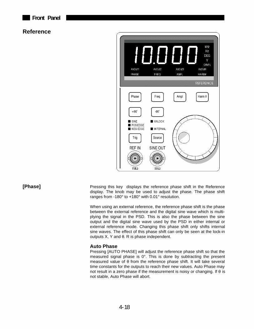
4-18
Front Panel
Reference
[Phase] Pressing this key displays the reference phase shift in the Referencedisplay. The knob may be used to adjust the phase. The phase shiftranges from -180° to +180° with 0.01° resolution.
When using an external reference, the reference phase shift is the phasebetween the external reference and the digital sine wave which is multi-plying the signal in the PSD. This is also the phase between the sineoutput and the digital sine wave used by the PSD in either internal orexternal reference mode. Changing this phase shift only shifts internalsine waves. The effect of this phase shift can only be seen at the lock-inoutputs X, Y and θ. R is phase independent.
Auto PhasePressing [AUTO PHASE] will adjust the reference phase shift so that themeasured signal phase is 0°. This is done by subtracting the presentmeasured value of θ from the reference phase shift. It will take severaltime constants for the outputs to reach their new values. Auto Phase maynot result in a zero phase if the measurement is noisy or changing. If θ isnot stable, Auto Phase will abort.
4-19
Front Panel
[+90°] and [-90°] The [+90°] and [-90°] keys add or subtract 90.000° from the referencephase shift. The phase does not need to be displayed to use these keys.
Zero PhasePressing the [+90°] and [-90°] keys together will set the reference phaseshift to 0.00°.
[Freq] Pressing this key displays the reference frequency in the Reference dis-play.
If the reference mode is external, then the measured reference frequencyis displayed. The knob does nothing in this case. If the harmonic numberis greater than 1 and the external reference goes above 102 kHz/Nwhere N is the harmonic number, then the harmonic number is reset to 1.The reference will always track the external reference signal.
If the reference mode is internal, then the internal oscillator frequency isdisplayed. The oscillator frequency may adjusted with the knob. The fre-quency has 4 1/2 digits or 0.1 mHz resolution, whichever is larger. Thefrequency can range from 0.001 Hz to 102.00 kHz. The upper limit isdecreased if the harmonic number is greater than 1. In this case, theupper limit is 102 kHz/N where N is the harmonic number.
[Ampl] Pressing this key displays the Sine Output Amplitude in the Referencedisplay. Use the knob to adjust the amplitude from 4 mVrms to 5 Vrmswith 2 mV resolution. The output impedance of the Sine Out is 50Ω. If thesignal is terminated in 50Ω, the amplitude will be half of the programmedvalue.
When the reference mode is internal, this is the excitation source provid-ed by the SR830. When an external reference is used, this sine outputprovides a sine wave phase locked to the external reference.
The rear panel TTL Output provides a TTL square wave at the referencefrequency. This square wave is generated by discriminating the zerocrossings of the sine output. This signal can provide a trigger or syncsignal to the experiment when the internal reference source is used. Thissignal is also available when the reference is externally provided. In thiscase, the TTL Output is phase locked to the external reference.
[Harm #] The SR830 can detect signals at harmonics of the reference frequency.The SR830 multiplies the input signal with digital sine waves at a multipleof the reference. Only signals at this harmonic will be detected. Signalsat the original reference frequency are not detected and are attenuatedas if they were noise.
Whenever the harmonic detect number is greater than 1, the HARM#indicator in the Reference display will flash to remind you that theSR830 is detecting signals at a multiple of the reference frequency.
Always check the harmonic detect number before making anymeasurements.
4-20
Front Panel
If the harmonic number is set to N, then the internal reference fre-quency is limited to 102 kHz/N.
If an external reference is used and the reference frequencyexceeds 102 kHz/N, then N is reset to 1. The SR830 will always trackthe external reference.
Pressing this key displays the harmonic number in the Reference dis-play. The harmonic number may be adjusted using the knob. Harmonicsup to 19999 times the reference can be detected as long as the harmonicfrequency does not exceed 102 kHz. An attempt to increase the harmon-ic frequency above 102 kHz will display the message 'hAr ovEr' indicat-ing harmonic number over range.
[Source] This key selects the reference mode. The normal mode is External refer-ence (no indicator). The Internal mode is indicated by the INTERNAL led.
When the reference source is External, the SR830 will phase lock to theexternal reference provided at the Reference Input BNC. The SR830 willlock to frequencies between 0.001 Hz and 102.0 kHz. Use the [Freq] keyto display the external frequency.
When the reference source is Internal, the SR830's synthesized internalreference is used as the reference. The Reference Input BNC is ignoredin this case. In this mode, the Sine Out or TTL Sync Out provides theexcitation for the measurement. Use the [Freq] key to display and adjustthe frequency.
[Trig] This key selects the external reference input trigger mode.
When either POS EDGE or NEG EDGE is selected, the SR830 locks tothe selected edge of a TTL square wave or pulse train. For reliable oper-ation, the TTL signal should exceed 3.5 V when high and be less then0.5 V when low. The input is directed past the analog discriminator and isDC coupled into a TTL input gate. This input mode should be used when-ever possible since it is less noise prone than the sine wave discrimina-tor.
For very low frequencies (<1 Hz), a TTL reference MUST be used.
SINE input mode locks the SR830 to the rising zero crossings of ananalog signal at the Reference Input BNC. This signal should be a cleansine wave at least 200 mVpk in amplitude. In this input mode, theReference Input is AC coupled (above 1 Hz) with an input impedance of1 MΩ.
Sine reference mode can not be used at frequencies far below 1 Hz.At very low frequencies, the TTL input modes must be used.
UNLOCK The UNLOCK indicator turns on if the SR830 can not lock to the externalreference.
4-21
Front Panel
Auto Functions
Pressing an Auto Function key initiates an auto function which may takesome time. The AUTO leds in the CH1 and CH2 displays will be on whilethe function is in progress. A multi-tone sound will indicate when the autofunction is complete and the AUTO leds will turn off.
[Auto Reserve] Pressing [AUTO RESERVE] will adjust the dynamic reserve to the mini-mum reserve required. To do this, the reserve is decreased until theanalog input amplifier is overloaded. The reserve is then increased toremove the overload.
Auto Reserve will work only if the overloading noise source has a fre-quency greater than a few Hz. Lower frequency noise sources may over-load so infrequently that Auto Reserve can not detect it.
[AUTO RESERVE] does not change the notch prefilter settings.
[Auto Gain] [AUTO GAIN] will adjust the sensitivity so that the detected signal magni-tude is a sizable percentage of full scale. Many time constants arerequired to determine whether a particular sensitivity will overload or not.Auto Gain thus takes a longer time when the time constant is long.
Auto Gain will not run if the time constant is greater than 1 secondsince the total time required could be far too long to be useful.
The message 'tc ovEr' will be displayed to indicate that the time constantis too long for Auto Gain to run.
[Auto Phase] [AUTO PHASE] adjusts the reference phase shift so that the measuredsignal phase is 0°. This is done by subtracting the measured value of θfrom the programmed reference phase shift. It will take several time con-stants for the outputs to reach their new values during which time θ willmove towards 0°. Do not press [AUTO PHASE] again until the outputshave stabilized. When the measurement is noisy or if the outputs arechanging, Auto Phase may not result in a zero phase.
Auto Phase will not run if the value of θ is unstable.
The message 'PhAS bAd' will be displayed to indicate that the phase isunstable and Auto Phase will not run.
Auto Setup There is no truly reliable way to automatically setup a lock-in amplifier for
4-22
Front Panel
all possible input signals. In most cases, the following procedure shouldsetup the SR830 to measure the input signal.
1.Press [AUTO GAIN] to set the sensitivity.
2.Press [AUTO RESERVE].
3.Adjust the time constant and roll-off until there is no Time Constantoverload.
4.Press [AUTO PHASE] if desired.
5.Repeat if necessary.
At very low frequencies, the auto functions may not function properly.This is because very low frequency signals overload very infrequentlyand the time constants used tend to be very long.
4-23
Front Panel
Setup
[Save] Nine amplifier setups may be stored in non-volatile memory.To save asetup, press [Save] to display the buffer number (1..9) in the CH2 dis-play. Use the knob to select the desired buffer number. Press [Save]again to store the setup in the buffer, or any other key to abort the saveprocess.
The message 'SAvE n donE' is displayed if the setup is successfullysaved. The message 'SAve not donE' is displayed if the save process isaborted.
[Recall] Nine amplifier setups may be stored in non-volatile memory.To recall asetup, press [Recall] to display the buffer number (1..9) in the CH2 dis-play. Use the knob to select the desired buffer number. Press [Recall]again to recall the setup in the buffer, or any other key to abort therecall process. When a setup is recalled, any data presently in the databuffer is lost.
The message 'rcal n donE' is displayed if the setup is successfullyrecalled. The message 'rcal not donE' is displayed if the recall process isaborted. The message 'rcal dAtA Err' is displayed if the recalled setup isnot valid. This is usually because a setup has never been saved into theselected buffer.
[Aux Out] The 4 Aux Outputs may be programmed from the front panel. Press[Aux Out] until the desired output (1-4) is displayed in the Reference dis-play. The AxOut indicators below the display indicate which output (1-4)is displayed. The knob may then be used to adjust the output level from-10.5V to +10.5V. Press [Phase], [Freq], [Ampl] or [Harm#] to return thedisplay to normal.
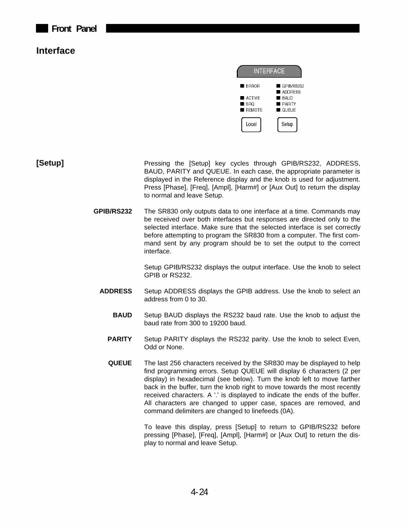
4-24
Front Panel
Interface
[Setup] Pressing the [Setup] key cycles through GPIB/RS232, ADDRESS,BAUD, PARITY and QUEUE. In each case, the appropriate parameter isdisplayed in the Reference display and the knob is used for adjustment.Press [Phase], [Freq], [Ampl], [Harm#] or [Aux Out] to return the displayto normal and leave Setup.
GPIB/RS232 The SR830 only outputs data to one interface at a time. Commands maybe received over both interfaces but responses are directed only to theselected interface. Make sure that the selected interface is set correctlybefore attempting to program the SR830 from a computer. The first com-mand sent by any program should be to set the output to the correctinterface.
Setup GPIB/RS232 displays the output interface. Use the knob to selectGPIB or RS232.
ADDRESS Setup ADDRESS displays the GPIB address. Use the knob to select anaddress from 0 to 30.
BAUD Setup BAUD displays the RS232 baud rate. Use the knob to adjust thebaud rate from 300 to 19200 baud.
PARITY Setup PARITY displays the RS232 parity. Use the knob to select Even,Odd or None.
QUEUE The last 256 characters received by the SR830 may be displayed to helpfind programming errors. Setup QUEUE will display 6 characters (2 perdisplay) in hexadecimal (see below). Turn the knob left to move fartherback in the buffer, turn the knob right to move towards the most recentlyreceived characters. A '.' is displayed to indicate the ends of the buffer.All characters are changed to upper case, spaces are removed, andcommand delimiters are changed to linefeeds (0A).
To leave this display, press [Setup] to return to GPIB/RS232 beforepressing [Phase], [Freq], [Ampl], [Harm#] or [Aux Out] to return the dis-play to normal and leave Setup.
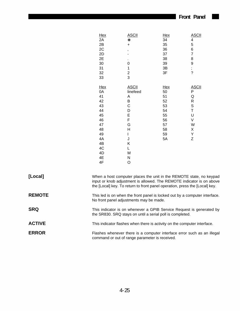
4-25
Front Panel
Hex ASCII Hex ASCII2A 34 42B + 35 52C , 36 62D - 37 72E . 38 830 0 39 931 1 3B ;32 2 3F ?33 3
Hex ASCII Hex ASCII0A linefeed 50 P41 A 51 Q42 B 52 R43 C 53 S44 D 54 T45 E 55 U46 F 56 V47 G 57 W48 H 58 X49 I 59 Y4A J 5A Z4B K4C L4D M4E N4F O
[Local] When a host computer places the unit in the REMOTE state, no keypadinput or knob adjustment is allowed. The REMOTE indicator is on abovethe [Local] key. To return to front panel operation, press the [Local] key.
REMOTE This led is on when the front panel is locked out by a computer interface.No front panel adjustments may be made.
SRQ This indicator is on whenever a GPIB Service Request is generated bythe SR830. SRQ stays on until a serial poll is completed.
ACTIVE This indicator flashes when there is activity on the computer interface.
ERROR Flashes whenever there is a computer interface error such as an illegalcommand or out of range parameter is received.
4-26
Front Panel
WARNING MESSAGES
The SR830 displays various warning messages whenever the operation of the instrument is not obvious. Thetwo tone warning alarm sounds when these messages are displayed.
Display Warning Message Meaning
LOCL LOut LOCAL LOCKOUT If the computer interface has placed the unit in the REMOTEstate, indicated by the REMOTE led, then the keys and the knobare disabled. Attempts to change the settings from the frontpanel will display this message.
IGAn chG IGAIN CHANGE Indicates that the current conversion gain has been changed to1 MΩ as a result of changing the sensitivity. Sensitivities from20 nA to 1 µA require 1 MΩ current gain.
tc chnG TC CHANGE Indicates that the time constant has been changed, either byincreasing the detection frequency from below 200 Hz to above200 Hz, or by changing the sensitivity, dynamic reserve, filterslope, or expand.
hAr ovEr HARMONIC OVER An attempt to increase the harmonic detect frequency above102 kHz will display this message.
tc ovEr TC OVER Indicates that the time constant is too long (>1s) for Auto Gain torun.
PhAS bAd PHASE BAD Indicates that the phase is unstable and Auto Phase will not run.
rcal dAtA Err RECALL DATA ERR This message is displayed if the recalled setup is not valid. Thisis usually because a setup has never been saved into the select-ed buffer.
undr UNDR Indicates unit may not be precisely locked at very low frequency.
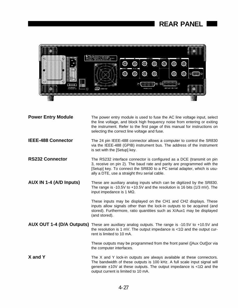
REAR PANEL
Power Entry Module The power entry module is used to fuse the AC line voltage input, selectthe line voltage, and block high frequency noise from entering or exitingthe instrument. Refer to the first page of this manual for instructions onselecting the correct line voltage and fuse.
IEEE-488 Connector The 24 pin IEEE-488 connector allows a computer to control the SR830via the IEEE-488 (GPIB) instrument bus. The address of the instrumentis set with the [Setup] key.
RS232 Connector The RS232 interface connector is configured as a DCE (transmit on pin3, receive on pin 2). The baud rate and parity are programmed with the[Setup] key. To connect the SR830 to a PC serial adapter, which is usu-ally a DTE, use a straight thru serial cable.
AUX IN 1-4 (A/D Inputs) These are auxiliary analog inputs which can be digitized by the SR830.The range is -10.5V to +10.5V and the resolution is 16 bits (1/3 mV). Theinput impedance is 1 MΩ.
These inputs may be displayed on the CH1 and CH2 displays. Theseinputs allow signals other than the lock-in outputs to be acquired (andstored). Furthermore, ratio quantities such as X/Aux1 may be displayed(and stored).
AUX OUT 1-4 (D/A Outputs) These are auxiliary analog outputs. The range is -10.5V to +10.5V andthe resolution is 1 mV. The output impedance is <1Ω and the output cur-rent is limited to 10 mA.
These outputs may be programmed from the front panel ([Aux Out])or viathe computer interfaces.
X and Y The X and Y lock-in outputs are always available at these connectors.The bandwidth of these outputs is 100 kHz. A full scale input signal willgenerate ±10V at these outputs. The output impedance is <1Ω and theoutput current is limited to 10 mA.
4-27
4-28
Rear Panel
These outputs are affected by the X and Y offsets and expands. Theactual outputs are
X Output = (X/sensitivity - offset)xExpandx10VY Output = (Y/sensitivity - offset)xExpandx10V
where the offset is a percentage of full scale and the expand is an integerfrom 1, 10 or 100. The offsets and expand are set from the front panel.
MONITOR OUT This BNC provides a buffered output from the signal amplifiers and prefil-ters. This is the signal just before the A/D converter and PSD. The outputimpedance is <1Ω and the output current is limited to 10 mA.
The gain from the signal input to the monitor output is the overall gainminus the dynamic reserve minus 3dB. The overall gain is 10V dividedby the sensitivity. The actual dynamic reserve is specified in the descrip-tion of the [Reserve] key. For example, if the sensitivity is 10 mV, thegain is 60dB. If the dynamic reserve is 20dB, then the gain from the inputto the monitor output is 60-20-3=37dB or a gain of 71. A 10 mV (rms)input will result in a .7 Vrms or1 Vpk output. The gain is only accurate toabout 1.5dB or 20%.
This output is useful for determining the cause of input overloads and theeffects of prefiltering. However, because the analog gain never exceeds2000, very small signals may not be amplified enough to viewed at themonitor output.
TRIG IN This TTL input may be used to trigger stored data samples and/or to startdata acquisition. If Trigger Start is selected, then a rising edge will startdata storage. If the sample rate is also Trigger, then samples are record-ed at every subsequent trigger. (The first trigger starts the scan andtakes the first data point, subsequent triggers record the rest of the datapoints.) When the sample rate is set to Trigger, samples are recordedwhenever there is a rising edge at the Trigger input. The maximumsample rate is 512 Hz. Data storage is available through the computerinterface only.
TTL OUT This output is the TTL sync output for the internal oscillator. The output isa square wave whose edges are linked to the sine wave zero crossings.This is useful when the sine output amplitude is small and a synchronoustrigger is required (to a scope for example). This output is active evenwhen locked to an external reference.
PREAMP CONNECTOR This 9 pin "D" connector provides power and control signals to externalpreamplifiers such as the SR550 and SR552. The power connections aredescribed below.
Pin Voltage1 +20V2 +5V6 -20V7 Signal Ground8 Ground
4-29
Rear Panel
Using SRS Preamps When using either the SR550 or SR552, connect the power cable (stan-dard 9 pin D connectors) from the preamp to the rear panel preamp con-nector on the SR830. Use BNC cables to connect the A output from thepreamp to the A input of the SR830. The B output from the preamp(preamp ground) may be connected to the B input of the SR830. In thiscase, use A-B as the input configuration. Be sure to twist the A and Bcables so that there is no differential noise pickup between the cables.
The SR550 and SR552 are AC coupled from 1 Hz to100 kHz. Set the SR830 to AC coupled since the signal must be above1 Hz. The SR550 has an input impedance of 100 MΩ, the SR552 has100 kΩ.
The SR830 does NOT compensate for the gain of thepreamp. The SR830 sets both preamps to their maximum gains.Measurements made by the SR830 with a preamp need to be divided bythe gain of the preamp. The SR550 has a gain of 10 and the SR552 hasa gain of 100.

4-30
Rear Panel
completed.To help find program errors, the SR830 can dis-play its receive buffer on the displays. Use the[Setup] key to access the QUEUE display. Thelast 256 characters received by the SR830 may bedisplayed in hexadecimal ASCII. See theOPERATION section for a complete description.
COMMAND SYNTAX
Communications with the SR830 uses ASCII char-acters. Commands may be in either UPPER orlower case and may contain any number ofembedded space characters. A command to theSR830 consists of a four character commandmnemonic, arguments if necessary, and a com-mand terminator. The terminator must be a line-feed <lf> or carriage return <cr> on RS232, or alinefeed <lf> or EOI on GPIB. No command pro-cessing occurs until a command terminator isreceived. Commands function identically on GPIBand RS232 whenever possible. Command mne-monics beginning with an asterisk "" are IEEE-488.2 (1987) defined common commands. Thesecommands also function identically on RS232.Commands may require one or more parameters.Multiple parameters are separated by commas (,).
Multiple commands may be sent on one commandline by separating them with semicolons (;). Thedifference between sending several commands onthe same line and sending several independentcommands is that when a command line is parsedand executed, the entire line is executed beforeany other device action proceeds.
There is no need to wait between commands. TheSR830 has a 256 character input buffer and pro-cesses commands in the order received. If thebuffer fills up, the SR830 will hold off handshakingon the GPIB and attempt to hold off handshakingon RS232. Similarly, the SR830 has a 256 charac-ter output buffer to store outputs until the hostcomputer is ready to receive. If either buffer over-flows, both buffers are cleared and an errorreported.
The present value of a particular parameter may
INTRODUCTION
The SR830 DSP Lock-in Amplifier may be remote-ly programmed via either the RS232 or GPIB(IEEE-488) interfaces. Any computer supportingone of these interfaces may be used to programthe SR830. Both interfaces are receiving at alltimes, however, the SR830 will send responsesto only one interface. Specify the output inter-face with the [Setup] key or use the OUTX com-mand at the beginning of every program todirect the responses to the correct interface.
COMMUNICATING WITH GPIB
The SR830 supports the IEEE-488.1 (1978) inter-face standard. It also supports the requiredcommon commands of the IEEE-488.2 (1987)standard. Before attempting to communicate withthe SR830 over the GPIB interface, the SR830'sdevice address must be set. The address is setwith the [Setup] key and may be set between 1and 30.
COMMUNICATING WITH RS232
The SR830 is configured as a DCE ( transmit onpin 3, receive on pin 2) device and supports CTS/DTR hardware handshaking. The CTS signal (pin5) is an output indicating that the SR830 is ready,while the DTR signal (pin 20) is an input that isused to control the SR830's data transmission. Ifdesired, the handshake pins may be ignored and asimple 3 wire interface (pins 2,3 and 7) may beused. The RS232 interface baud rate and paritymust be set. These are set with the [Setup] key.The RS232 word length is always 8 bits.
STATUS INDICATORS AND QUEUES
To assist in programming, the SR830 has 4 inter-face status indicators. The ACTIVE indicator flash-es whenever a character is received or transmittedover either interface. The ERROR indicator flash-es when an error, such as an illegal command, orparameter out of range, has been detected. TheREMOTE indicator is on whenever the SR830 is ina remote state (front panel locked out). The SRQindicator is on when the SR830 generates a ser-vice request. SRQ stays on until a serial poll is
REMOTE PROGRAMMING
5-1
5-2
Remote Programming
be determined by querying the SR830 for itsvalue. A query is formed by appending a questionmark "?" to the command mnemonic and omittingthe desired parameter(s) from the command.Values returned by the SR830 are sent as a stringof ASCII characters terminated by a carriagereturn <cr> on RS232 and by a line-feed <lf> onGPIB. If multiple queries are sent on one com-mand line (separated by semicolons, of course)the answers will be returned individually, each witha terminator.
Examples of Command Formats
FMOD 1 <lf> Set reference source tointernal
FREQ 10E3 <lf> Set the internal reference fre-quency to 10000 Hz (10 kHz)
IDN? <lf> Queries the deviceidentification
STRT <lf> Starts data acquisitionOUTP? 1 <lf> Queries the value of X
INTERFACE READY AND STATUS
The Interface Ready bit (bit 1) in the Serial PollStatus Byte signals that the SR830 is ready toreceive and execute a command. When a com-mand is received, this bit is cleared indicating thatan operation is in progress. While the operation isin progress, no other commands will be pro-cessed. Commands received during this time arestored in the buffer to be processed later. OnlyGPIB serial polling will generate a response whilea command is in progress. When the commandexecution terminates, the Interface Ready bit is setagain and new commands will be processed.Since most commands execute very quickly, thehost computer does not need to continually checkthe Interface Ready bit. Commands may be sentone after another and they will be processedimmediately.
When using the GPIB interface, serial polling maybe used to check the Interface Ready bit in theSerial Poll Byte while an operation is in progress.After the Interface Ready bit becomes set, signal-ling the completion of the command, then the ERRor ESB bit may be checked to verify successfulcompletion of the command.
If the RS232 interface is used, or serial polling isnot available, then the STB?, ESR?, ERRS?,
and LIAS? status query commands may be usedto query the Status Bytes. Since the SR830 pro-cesses one command at a time, the status querywill not be processed until the previous operationis finished. Thus a response to the status query initself signals that the previous command is fin-ished. The query response may then be checkedfor various errors.
GET (GROUP EXECUTE TRIGGER)
The GPIB interface command GET is the same asthe TRIG command. GET is the same as a triggerinput. GET only has an effect if the sampling rateis triggered or if triggers start a scan.
5-3
Remote Programming
DETAILED COMMAND LIST
The four letter mnemonic in each command sequence specifies the command. The rest of the sequence con-sists of parameters. Multiple parameters are separated by commas. Parameters shown in are optional ormay be queried while those not in are required. Commands that may be queried have a question mark inparentheses (?) after the mnemonic. Commands that may ONLY be queried have a ? after the mnemonic.Commands that MAY NOT be queried have no ?. Do not send ( ) or as part of the command.
The variables are defined as follows. i, j, k, l, m integersx, y, z real numbersf frequencys string
All numeric variables may be expressed in integer, floating point or exponential formats ( i.e., the number fivecan be either 5, 5.0, or .5E1). Strings are sent as a sequence of ASCII characters.
Remember!All responses are directed only to the selected output interface!
Use the OUTX command to select the correct interface at the beginning of everyprogram.
5-4
Remote Programming
REFERENCE and PHASE COMMANDS
PHAS (?) x The PHAS command sets or queries the reference phase shift. Theparameter x is the phase (real number of degrees). The PHAS x com-mand will set the phase shift to x. The value of x will be rounded to 0.01°.The phase may be programmed from -360.00 ≤ x ≤ 729.99 and will bewrapped around at ±180°. For example, the PHAS 541.0 command willset the phase to -179.00° (541-360=181=-179). The PHAS? queries thephase shift.
FMOD (?) i The FMOD command sets or queries the reference source. The parame-ter i selects internal (i=1) or external (i=0).
FREQ (?) f The FREQ command sets or queries the reference frequency. TheFREQ? query command will return the reference frequency (in internal orexternal mode).
The FREQ f command sets the frequency of the internal oscillator. Thiscommand is allowed only if the reference source is internal. The parame-ter f is a frequency (real number of Hz). The value of f will be rounded to5 digits or 0.0001 Hz, whichever is greater. The value of f is limited to0.001 ≤ f ≤ 102000. If the harmonic number is greater than 1, then thefrequency is limited to nxf ≤ 102 kHz where n is the harmonic number.
RSLP (?) i The RSLP command sets or queries the reference trigger when using theexternal reference mode. The parameter i selects sine zero crossing(i=0), TTL rising edge (i=1), , or TTL falling edge (i=2). At frequenciesbelow 1 Hz, the a TTL reference must be used.
HARM (?) i The HARM command sets or queries the detection harmonic. Thisparameter is an integer from 1 to 19999. The HARM i command will setthe lock-in to detect at the ith harmonic of the reference frequency. Thevalue of i is limited by ixf ≤ 102 kHz. If the value of i requires a detectionfrequency greater than 102 kHz, then the harmonic number will be set tothe largest value of i such that ixf ≤ 102 kHz.
SLVL (?) x The SLVL command sets or queries the amplitude of the sine output.The parameter x is a voltage (real number of Volts). The value of x willbe rounded to 0.002V. The value of x is limited to 0.004 ≤ x ≤ 5.000.
5-5
Remote Programming
INPUT and FILTER COMMANDS
ISRC (?) i The ISRC command sets or queries the input configuration. The parame-ter i selects A (i=0), A-B (i=1), I (1 MΩ) (i=2) or I (100 MΩ) (i=3).
Changing the current gain does not change the instrument sensitivity.Sensitivities above 10 nA require a current gain of 1 MΩ. Sensitivitiesbetween 20 nA and 1 µA automatically select the 1 MΩ current gain. Atsensitivities below 20 nA, changing the sensitivity does not change thecurrent gain.
IGND (?) i The IGND command sets or queries the input shield grounding. Theparameter i selects Float (i=0) or Ground (i=1).
ICPL (?) i The ICPL command sets or queries the input coupling. The parameter iselects AC (i=0) or DC (i=1).
ILIN (?) i The ILIN command sets or queries the input line notch filter status. Theparameter i selects Out or no filters (i=0), Line notch in (i=1), 2xLinenotch in (i=2) or Both notch filters in (i=3).
5-6
Remote Programming
GAIN and TIME CONSTANT COMMANDS
SENS (?) i The SENS command sets or queries the sensitivity. The parameter iselects a sensitivity below.
i sensitivity i sensitivity0 2 nV/fA 13 50 µV/pA1 5 nV/fA 14 100 µV/pA2 10 nV/fA 15 200 µV/pA3 20 nV/fA 16 500 µV/pA4 50 nV/fA 17 1 mV/nA5 100 nV/fA 18 2 mV/nA6 200 nV/fA 19 5 mV/nA7 500 nV/fA 20 10 mV/nA8 1 µV/pA 21 20 mV/nA9 2 µV/pA 22 50 mV/nA10 5 µV/pA 23 100 mV/nA11 10 µV/pA 24 200 mV/nA12 20 µV/pA 25 500 mV/nA
26 1 V/µA
RMOD (?) i The RMOD command sets or queries the reserve mode. The parameter iselects High Reserve (i=0), Normal (i=1) or Low Noise (minimum) (i=2).See the description of the [Reserve] key for the actual reserves for eachsensitivity.
OFLT (?) i The OFLT command sets or queries the time constant. The parameter iselects a time constant below.
i time constant i time constant0 10 µs 10 1 s1 30 µs 11 3 s2 100 µs 12 10 s3 300 µs 13 30 s4 1 ms 14 100 s5 3 ms 15 300 s6 10 ms 16 1 ks7 30 ms 17 3 ks8 100 ms 18 10 ks9 300 ms 19 30 ks
Time constants greater than 30s may NOT be set if theharmonic x ref. frequency (detection frequency) exceeds 200 Hz. Timeconstants shorter than the minimum time constant (based upon the filterslope and dynamic reserve) will set the time constant to the minimumallowed time constant. See the Gain and TIme Constant operationsection.
OFSL (?) i The OFSL command sets or queries the low pass filter slope. Theparameter i selects 6 dB/oct (i=0), 12 dB/oct (i=1), 18 dB/oct (i=2) or24 dB/oct (i=3).

5-7
Remote Programming
SYNC (?) i The SYNC command sets or queries the synchronous filter status. Theparameter i selects Off (i=0) or synchronous filtering below 200 Hz (i=1).Synchronous filtering is turned on only if the detection frequency (refer-ence x harmonic number) is less than 200 Hz.
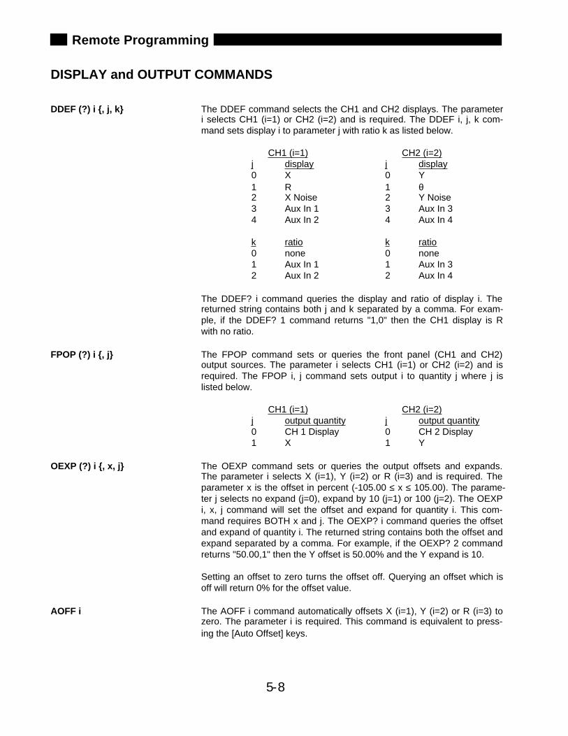
5-8
Remote Programming
DISPLAY and OUTPUT COMMANDS
DDEF (?) i , j, k The DDEF command selects the CH1 and CH2 displays. The parameteri selects CH1 (i=1) or CH2 (i=2) and is required. The DDEF i, j, k com-mand sets display i to parameter j with ratio k as listed below.
CH1 (i=1) CH2 (i=2)j display j display0 X 0 Y1 R 1 θ2 X Noise 2 Y Noise3 Aux In 1 3 Aux In 34 Aux In 2 4 Aux In 4
k ratio k ratio0 none 0 none1 Aux In 1 1 Aux In 32 Aux In 2 2 Aux In 4
The DDEF? i command queries the display and ratio of display i. Thereturned string contains both j and k separated by a comma. For exam-ple, if the DDEF? 1 command returns "1,0" then the CH1 display is Rwith no ratio.
FPOP (?) i , j The FPOP command sets or queries the front panel (CH1 and CH2)output sources. The parameter i selects CH1 (i=1) or CH2 (i=2) and isrequired. The FPOP i, j command sets output i to quantity j where j islisted below.
CH1 (i=1) CH2 (i=2)j output quantity j output quantity0 CH 1 Display 0 CH 2 Display1 X 1 Y
OEXP (?) i , x, j The OEXP command sets or queries the output offsets and expands.The parameter i selects X (i=1), Y (i=2) or R (i=3) and is required. Theparameter x is the offset in percent (-105.00 ≤ x ≤ 105.00). The parame-ter j selects no expand (j=0), expand by 10 (j=1) or 100 (j=2). The OEXPi, x, j command will set the offset and expand for quantity i. This com-mand requires BOTH x and j. The OEXP? i command queries the offsetand expand of quantity i. The returned string contains both the offset andexpand separated by a comma. For example, if the OEXP? 2 commandreturns "50.00,1" then the Y offset is 50.00% and the Y expand is 10.
Setting an offset to zero turns the offset off. Querying an offset which isoff will return 0% for the offset value.
AOFF i The AOFF i command automatically offsets X (i=1), Y (i=2) or R (i=3) tozero. The parameter i is required. This command is equivalent to press-ing the [Auto Offset] keys.
5-9
Remote Programming
AUX INPUT and OUTPUT COMMANDS
OAUX? i The OAUX? command queries the Aux Input values. The parameter iselects an Aux Input (1, 2, 3 or 4) and is required. The Aux Input voltagesare returned as ASCII strings with units of Volts. The resolution is1/3 mV. This command is a query only command.
AUXV (?) i , x The AUXV command sets or queries the Aux Output voltage when theoutput. The parameter i selects an Aux Output (1, 2, 3 or 4) and isrequired. The parameter x is the output voltage (real number of Volts)and is limited to -10.500 ≤ x ≤ 10.500. The output voltage will be set tothe nearest mV.
5-10
Remote Programming
SETUP COMMANDS
OUTX (?) i The OUTX command sets the output interface to RS232 (i=0) or GPIB(i=1). The OUTX i command should be sent before any query com-mands to direct the responses to the interface in use.
OVRM i In general, every GPIB interface command will put the SR830 into theREMOTE state with the front panel deactivated. To defeat this feature,use the OVRM 1 command to overide the GPIB remote. In this mode, thefront panel is not locked out when the unit is in the REMOTE state. TheOVRM 0 command returns the unit to normal remote operation.
KCLK (?) i The KCLK command sets or queries the key click On (i=1) or Off (i=0)state.
ALRM (?) i The ALRM command sets or queries the alarm On (i=1) or Off (i=0)state.
SSET i The SSET i command saves the lock-in setup in setting buffer i (1≤i≤9).The setting buffers are retained when the power is turned off.
RSET i The RSET i command recalls the lock-in setup from setting buffer i(1≤i≤9). Interface parameters are not changed when a setting buffer isrecalled with the RSET command. If setting i has not been saved prior tothe RSET i command, then an error will result.
5-11
Remote Programming
AUTO FUNCTIONS
AGAN The AGAN command performs the Auto Gain function. This command isthe same as pressing the [Auto Gain] key. Auto Gain may take sometime if the time constant is long. AGAN does nothing if the time constantis greater than 1 second. Check the command execution in progress bitin the Serial Poll Status Byte (bit 1) to determine when the function isfinished.
ARSV The ARSV command performs the Auto Reserve function. This com-mand is the same as pressing the [Auto Reserve] key. Auto Reservemay take some time. Check the command execution in progress bit inthe Serial Poll Status Byte (bit 1) to determine when the function isfinished.
APHS The APHS command performs the Auto Phase function. This commandis the same as pressing the [Auto Phase] key. The outputs will take manytime constants to reach their new values. Do not send the APHS com-mand again without waiting the appropriate amount of time. If the phaseis unstable, then APHS will do nothing. Query the new value of the phaseshift to see if APHS changed the phase shift.
AOFF i The AOFF i command automatically offsets X (i=1), Y (i=2) or R (i=3) tozero. The parameter i is required. This command is equivalent to press-ing the [Auto Offset] keys.
5-12
Remote Programming
DATA STORAGE COMMANDS
Data StorageThe SR830 can store up to 16383 points from both the Channel 1 and Channel 2 displays in an internal databuffer. The data buffer is NOT retained when the power is turned off. The data buffer is accessible only viathe computer interface.
Configure the displays to show the desired quantity (with appropriate ratio, offset and expand). The databuffer stores the quantities which are displayed. Only quantities which are displayed on the CH1 or CH2 dis-plays can be stored. Frequency, for example, can not be stored.
Data Points and BinsData points stored in the buffer are sometimes referred to by their bin position within the buffer. The oldestdata point is bin0, the next point is bin1, etc. A buffer with N points numbers them from 0 to N-1.
Sample RateThe Sample Rate can be varied from 512 Hz down to 62.5 mHz (1 point every 16 sec). The sample rate setshow often points are added to the storage buffer. Both displays are sampled at the same rate (and at thesame times).
In addition to the internal sample rates, samples can be triggered by an external TTL trigger. In this mode, asample is recorded within 2 ms of a rising edge trigger on the rear panel Trigger input. Triggers which occurfaster than 512 Hz are ignored.
Storage TimeThe buffer holds 16383 samples taken at the sample rate. The entire storage time is 16383 divided by thesample rate.
End of ScanWhen the buffer becomes full, data storage can stop or continue.
The first case is called 1 Shot (data points are stored for a single buffer length). At the end of the buffer, datastorage stops and an audio alarm sounds.
The second case is called Loop. In this case, data storage continues at the end of the buffer. The data bufferwill store 16383 points and start storing at the beginning again. The most recent 16383 points will be con-tained in the buffer. Once the buffer has looped around, the oldest point (at any time) is at bin#0 and the mostrecent point is at bin#16382.
The default mode is Loop.
Starting and Stopping a ScanThe STRT, PAUS and REST commands are used to control data storage. Basically, the STRT commandstarts data storage after a reset or pause. The PAUS command pauses data storage but does not reset thebuffer. The REST stops data storage and resets the buffer data.
In addition, the rear panel Trigger input can be used to start data storage. To select this mode, use the TSTRcommand. In this mode, a rising TTL trigger will act the same as the STRT command. The sample rate canbe either internal or Triggered. In the first case, the trigger starts the storage and data is sampled at the pro-grammed sample rate (up to 512 Hz). In the latter case, the first trigger will start the storage and data will besampled at every subsequent trigger.
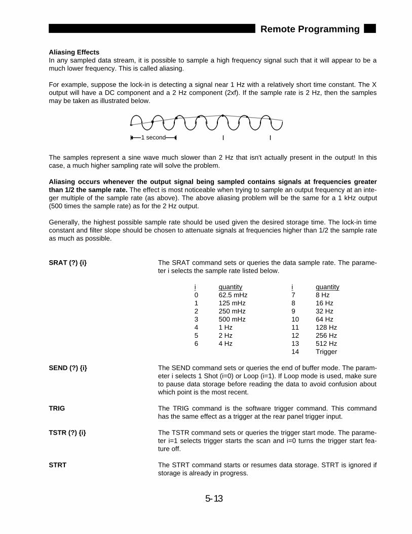
5-13
Remote Programming
Aliasing EffectsIn any sampled data stream, it is possible to sample a high frequency signal such that it will appear to be amuch lower frequency. This is called aliasing.
For example, suppose the lock-in is detecting a signal near 1 Hz with a relatively short time constant. The Xoutput will have a DC component and a 2 Hz component (2xf). If the sample rate is 2 Hz, then the samplesmay be taken as illustrated below.
The samples represent a sine wave much slower than 2 Hz that isn't actually present in the output! In thiscase, a much higher sampling rate will solve the problem.
Aliasing occurs whenever the output signal being sampled contains signals at frequencies greaterthan 1/2 the sample rate. The effect is most noticeable when trying to sample an output frequency at an inte-ger multiple of the sample rate (as above). The above aliasing problem will be the same for a 1 kHz output(500 times the sample rate) as for the 2 Hz output.
Generally, the highest possible sample rate should be used given the desired storage time. The lock-in timeconstant and filter slope should be chosen to attenuate signals at frequencies higher than 1/2 the sample rateas much as possible.
SRAT (?) i The SRAT command sets or queries the data sample rate. The parame-
ter i selects the sample rate listed below.
i quantity i quantity0 62.5 mHz 7 8 Hz1 125 mHz 8 16 Hz2 250 mHz 9 32 Hz3 500 mHz 10 64 Hz4 1 Hz 11 128 Hz5 2 Hz 12 256 Hz6 4 Hz 13 512 Hz
14 Trigger
SEND (?) i The SEND command sets or queries the end of buffer mode. The param-eter i selects 1 Shot (i=0) or Loop (i=1). If Loop mode is used, make sureto pause data storage before reading the data to avoid confusion aboutwhich point is the most recent.
TRIG The TRIG command is the software trigger command. This commandhas the same effect as a trigger at the rear panel trigger input.
TSTR (?) i The TSTR command sets or queries the trigger start mode. The parame-ter i=1 selects trigger starts the scan and i=0 turns the trigger start fea-ture off.
STRT The STRT command starts or resumes data storage. STRT is ignored ifstorage is already in progress.
1 second

5-14
Remote Programming
PAUS The PAUS command pauses data storage. If storage is already pausedor reset then this command is ignored.
REST The REST command resets the data buffers. The REST command canbe sent at any time - any storage in progress, paused or not, will bereset. This command will erase the data buffer.
5-15
Remote Programming
DATA TRANSFER COMMANDS
OUTP ? i The OUTP? i command reads the value of X, Y, R or θ. The parameteri selects X (i=1), Y (i=2), R (i=3) or θ (i=4). Values are returned as ASCIIfloating point numbers with units of Volts or degrees. For example, theresponse might be "-1.01026". This command is a query only command.
OUTR ? i The OUTR? i command reads the value of the CH1 or CH2 display.The parameter i selects the display (i=1 or 2). Values are returned asASCII floating point numbers with units of the display. For example, theresponse might be "-1.01026". This command is a query only command.
SNAP ? i,j ,k,l,m,n The SNAP? command records the values of either 2, 3, 4, 5 or 6 param-eters at a single instant. For example, SNAP? is a way to query values ofX and Y (or R and θ) which are taken at the same time. This is importantwhen the time constant is very short. Using the OUTP? or OUTR? com-mands will result in time delays, which may be greater than the time con-stant, between reading X and Y (or R and θ).
The SNAP? command requires at least two parameters and at most sixparameters. The parameters i, j, k, l, m, n select the parameters below.
i,j,k,l,m,n parameter1 X2 Y3 R4 θ5 Aux In 16 Aux In 27 Aux In 38 Aux In 49 Reference Frequency10 CH1 display11 CH2 display
The requested values are returned in a single string with the values sep-arated by commas and in the order in which they were requested. Forexample, the SNAP?1,2,9,5 will return the values of X, Y, Freq andAux In 1. These values will be returned in a single string such as"0.951359,0.0253297,1000.00,1.234".The first value is X, the second is Y, the third is f, and the fourth isAux In 1.
The values of X and Y are recorded at a single instant. The values of Rand θ are also recorded at a single instant. Thus reading X,Y OR R,θyields a coherent snapshot of the output signal. If X,Y,R and θ are allread, then the values of X,Y are recorded approximately 10µs apart fromR,θ. Thus, the values of X and Y may not yield the exact values of R andθ from a single SNAP? query.
The values of the Aux Inputs may have an uncertainty of up to 32µs. Thefrequency is computed only every other period or 40 ms, whichever islonger.
5-16
Remote Programming
The SNAP? command is a query only command. The SNAP? commandis used to record various parameters simultaneously, not to transfer dataquickly.
OAUX? i The OAUX? command reads the Aux Input values. The parameter iselects an Aux Input (1, 2, 3 or 4) and is required. The Aux Input voltagesare returned as ASCII strings with units of Volts. The resolution is1/3 mV. This command is a query only command.
SPTS ? The SPTS? command queries the number of points stored in the buffer.Both displays have the same number of points. If the buffer is reset, then0 is returned. Remember, SPTS? returns N where N is the number ofpoints - the points are numbered from 0 (oldest) to N-1 (most recent).The SPTS? command can be sent at any time, even while storage is inprogress. This command is a query only command.
TRCA ? i, j, k The TRCA? command queries the points stored in the Channel i buffer.The values are returned as ASCII floating point numbers with the units ofthe trace. Multiple points are separated by commas and the final point isfollowed by a terminator. For example, the response with two pointsmight be "-1.234567e-009,+7.654321e-009,".
The parameter i selects the display buffer (i=1, 2) and is required. Pointsare read from the buffer starting at bin j (j≥0). A total of k bins are read(k≥1). To read a single point, set k=1. Both j and k are required. If j+kexceeds the number of stored points (as returned by the SPTS? query),then an error occurs. Remember, SPTS? returns N where N is the totalnumber of bins - the TRCA? command numbers the bins from 0 (oldest)to N-1 (most recent). If data storage is set to Loop mode, make sure thatstorage is paused before reading any data. This is because the pointsare indexed relative to the most recent point which is continuallychanging.
TRCB ? i, j, k The TRCB? command queries the points stored in the Channel i buffer.The values are returned as IEEE format binary floating point numbers(with the units of the trace). There are 4 bytes per point. Multiple pointsare not separated by any delimiter. The bytes can be read directly into afloating point array (in most languages).
Do not query the IFC (no command in progress) status bit after sendingthe TRCB command. This bit will not be set until the transfer is complete.
When using the GPIB interface, EOI is sent with the final byte. The pointsmust be read using a binary transfer (see your GPIB interface card soft-ware manual). Make sure that the software is configured to NOT termi-nate reading upon receipt of a CR or LF.
When using the RS232 interface, the word length must be 8 bits. Thepoints must be read as binary bytes (no checking for linefeeds, carriagereturns or other control characters). Most serial interface drivers aredesigned for ASCII text only and will not work here. In addition, the datatransfer does not pause between bytes. The receiving interface mustalways be ready to receive the next byte. In general, using binary trans-
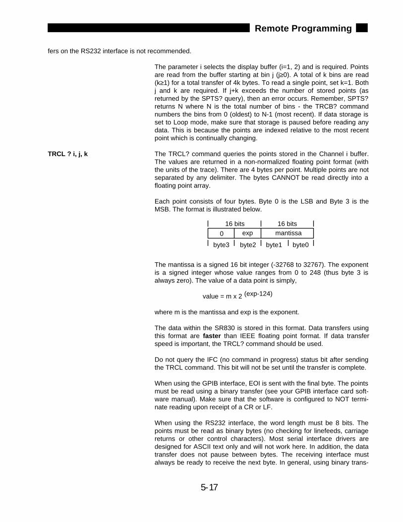
5-17
Remote Programming
fers on the RS232 interface is not recommended.
The parameter i selects the display buffer (i=1, 2) and is required. Pointsare read from the buffer starting at bin j (j≥0). A total of k bins are read(k≥1) for a total transfer of 4k bytes. To read a single point, set k=1. Bothj and k are required. If j+k exceeds the number of stored points (asreturned by the SPTS? query), then an error occurs. Remember, SPTS?returns N where N is the total number of bins - the TRCB? commandnumbers the bins from 0 (oldest) to N-1 (most recent). If data storage isset to Loop mode, make sure that storage is paused before reading anydata. This is because the points are indexed relative to the most recentpoint which is continually changing.
TRCL ? i, j, k The TRCL? command queries the points stored in the Channel i buffer.The values are returned in a non-normalized floating point format (withthe units of the trace). There are 4 bytes per point. Multiple points are notseparated by any delimiter. The bytes CANNOT be read directly into afloating point array.
Each point consists of four bytes. Byte 0 is the LSB and Byte 3 is theMSB. The format is illustrated below.
The mantissa is a signed 16 bit integer (-32768 to 32767). The exponentis a signed integer whose value ranges from 0 to 248 (thus byte 3 isalways zero). The value of a data point is simply,
value = m x 2 (exp-124)
where m is the mantissa and exp is the exponent.
The data within the SR830 is stored in this format. Data transfers usingthis format are faster than IEEE floating point format. If data transferspeed is important, the TRCL? command should be used.
Do not query the IFC (no command in progress) status bit after sendingthe TRCL command. This bit will not be set until the transfer is complete.
When using the GPIB interface, EOI is sent with the final byte. The pointsmust be read using a binary transfer (see your GPIB interface card soft-ware manual). Make sure that the software is configured to NOT termi-nate reading upon receipt of a CR or LF.
When using the RS232 interface, the word length must be 8 bits. Thepoints must be read as binary bytes (no checking for linefeeds, carriagereturns or other control characters). Most serial interface drivers aredesigned for ASCII text only and will not work here. In addition, the datatransfer does not pause between bytes. The receiving interface mustalways be ready to receive the next byte. In general, using binary trans-
exp mantissa16 bits 16 bits
0
byte3 byte2 byte1 byte0
5-18
Remote Programming
always be ready to receive the next byte. In general, using binary trans-fers on the RS232 interface is not recommended.
The parameter i selects the display buffer (i=1, 2) and is required. Pointsare read from the buffer starting at bin j (j≥0). A total of k bins are read(k≥1) for a total transfer of 4k bytes. To read a single point, set k=1. Bothj and k are required. If j+k exceeds the number of stored points (asreturned by the SPTS? query), then an error occurs. Remember, SPTS?returns N where N is the total number of bins - the TRCB? commandnumbers the bins from 0 (oldest) to N-1 (most recent). If data storage isset to Loop mode, make sure that storage is paused before reading anydata. This is because the points are indexed relative to the most recentpoint which is continually changing.
FAST (?) i The FAST command sets the fast data transfer mode on and off. Theparameter i selects On (i=1) or Off (i=0). When the fast transfer mode ison, whenever data is sampled and stored, the values of X and Y areautomatically transmitted over the GPIB interface (this mode is not avail-able over RS232). The sample rate sets the frequency of the data trans-fers. It is important that the receiving interface be able to keep up withthe transfers. FAST only sends data when data is being stored. If thestorage buffer is single-shot and full, then no data will be transferred.
The values of X and Y are transferred as signed integers, 2 bytes long(16 bits). X is sent first followed by Y for a total of 4 bytes per sample.The values range from -32768 to 32767. The value ±30000 represents±full scale (i.e. the sensitivity).
Offsets and expands are included in the values of X and Y. The trans-ferred values are (raw data - offset) x expand. The resulting value muststill be a 16 bit integer. The value ±30000 now represents ±full scaledivided by the expand factor.
At fast sample rates, it is important that the receiving interface be able tokeep up. If the SR830 finds that the interface is not ready to receive apoint, then the fast transfer mode is turned off.
The fast transfer mode may be turned off with the FAST0 command.
Make sure that the SR830 transmit buffer is empty by doing a dummyquery before a FAST transfer (for example, send SPTS? and read theanswer and ignore it). The transfer mode should be turned on (usingFAST1) before storage is started. Then use the STRD command (seebelow) to start data storage. After sending the STRD command, immedi-ately make the SR830 a talker and the controlling interface a listener.Remember, the first transfer will occur with the very first point.
STRD After using FAST1 to turn on fast data transfer, use the STRD commandto start the data storage. STRD starts data storage after a delay of 0.5sec. This delay allows the controlling interface to place itself in the readmode before the first data points are transmitted. Do not use the STRTcommand to start the scan. See the programming examples at the endof this section.
5-19
Remote Programming
INTERFACE COMMANDS
RST The RST command resets the SR830 to its default configurations. Thecommunications setup is not changed. All other modes and settings areset to their default conditions and values. This command takes sometime to complete. This command resets any data scan in progress. Datastored in the buffers will be lost.
IDN? The IDN? query returns the SR830's device identification string. Thisstring is in the format
"Stanford_Research_Systems,SR830,s/n00111,ver1.000".
In this example, the serial number is 00111 and the firmware version is1.000.
LOCL (?) i The LOCL command sets the local/remote function. If i=0 the SR830 isLOCAL, if i=1 the SR830 will go REMOTE, and if i=2 the SR830 will gointo LOCAL LOCKOUT state. The states duplicate the GPIB local/remotestates. In the LOCAL state both command execution and keyboard inputare allowed. In the REMOTE state command execution is allowed but thekeyboard and knob are locked out except for the [LOCAL] key whichreturns the SR830 to the LOCAL state. In the LOCAL LOCKOUT state allfront panel operation is locked out, including the [LOCAL] key.
The REMOTE indicator is directly above the [LOCAL] key.
The Overide Remote mode must be set to No in order for the front panelto be locked out. If Overide Remote is Yes, then the front panel is activeeven in the REMOTE state.
OVRM (?) i The OVRM command sets or queries the GPIB Overide Remote Yes/Nocondition. The parameter i selects No (i=0) or Yes (i=1). When OverideRemote is set to Yes, then the front panel is not locked out when the unitis in the REMOTE state. The REMOTE indicator will still be on and the[LOCAL] key will still return the unit to the Local state.
The default mode is Overide Remote Yes. To lock-out the front panel,use the OVRM0 command before local lock-out.
TRIG The TRIG command is the software trigger command. This commandhas the same effect as a trigger at the rear panel trigger input.
5-20
Remote Programming
STATUS REPORTING COMMANDS
The Status Byte definitions follow this section.
CLS The CLS command clears all status registers. The status enable regis-ters are NOT cleared.
ESE (?) i ,j The ESE i command sets the standard event enable register to thedecimal value i (0-255). The ESE i,j command sets bit i (0-7) to j (0 or1). The ESE? command queries the value (0-255) of the status byteenable register. The ESE? i command queries the value (0 or 1) of bit i.
ESR? i The ESR? command queries the value of the standard event statusbyte. The value is returned as a decimal number from 0 to 255. TheESR? i command queries the value (0 or 1) of bit i (0-7). Reading theentire byte will clear it while reading bit i will clear just bit i.
SRE (?) i ,j The SRE i command sets the serial poll enable register to the deci-mal value i (0-255). The SRE i,j command sets bit i (0-7) to j (0 or1).The SRE? command queries the value (0-255) of the serial pollenable register. The SRE? i command queries the value (0 or 1) of bit i.
STB? i The STB? command queries the value of the serial poll status byte.The value is returned as a decimal number from 0 to 255. The STB? icommand queries the value (0 or 1) of bit i (0-7). Reading this byte hasno effect on its value.
PSC (?) i The PSC command sets the value of the power-on status clear bit. Ifi=1 the power-on status clear bit is set and all status registers and enableregisters are cleared on power up. If i=0 the bit is cleared and the statusenable registers maintain their values at power down. This allows a ser-vice request to be generated at power up.
ERRE (?) i ,j The ERRE i command sets the error status enable register to the deci-mal value i (0-255). The ERRE i,j command sets bit i (0-7) to j (0 or 1).The ERRE? command queries the value (0-255) of the error statusenable register. The ERRE? i command queries the value (0 or 1) of bit i.
ERRS? i The ERRS? command queries the value of the error status byte. Thevalue is returned as a decimal number from 0 to 255. The ERRS? i com-mand queries the value (0 or 1) of bit i (0-7). Reading the entire byte willclear it while reading bit i will clear just bit i.
LIAE (?) i ,j The LIAE command sets the lock-in (LIA) status enable register to thedecimal value i (0-255). The LIAE i,j command sets bit i (0-7) to j (0 or 1).The LIAE? command queries the value of the LIA status enable register.The LIAE? i command queries the value (0 or 1) of bit i.
LIAS? i The LIAS? command queries the value of the lock-in (LIA) status byte.The value is returned as a decimal number from 0 to 255. The LIAS? icommand queries the value (0 or 1) of bit i (0-7). Reading the entire bytewill clear it while reading bit i will clear just bit i.
5-21
Remote Programming
STATUS BYTE DEFINITIONS
The SR830 reports on its status by means of four status bytes: the Serial Poll Status byte, the Standard EventStatus byte, the LIA Status byte, and the Error Status byte.
The status bits are set to 1 when the event or state described in the tables below has occurred or is present.
SERIAL POLL bit name usageSTATUS BYTE
0 SCN No scan in progress (Stop or Done). A Pausedscan is considered to be in progress.
1 IFC No command execution in progress.
2 ERR An enabled bit in the error status byte has beenset.
3 LIA An enabled bit in the LIA status byte has beenset.
4 MAV The interface output buffer is non-empty.
5 ESB An enabled bit in the standard status byte hasbeen set.
6 SRQ SRQ (service request) has occurred.
7 Unused
The ERR, LIA, and ESB bits are set whenever any bit in both their respective status bytes AND enable regis-ters is set. Use the SRE, ESE, ERRE and LIAE commands to set enable register bits. The ERR, LIA andESB bits are not cleared until ALL enabled status bits in the Error, LIA and Standard Event status bytes arecleared (by reading the status bytes or using CLS).
Using STB? to read the Serial Poll Status Byte
A bit in the Serial Poll status byte is NOT cleared by reading the status byte using STB?. The bit stays setas long as the status condition exists. This is true even for SRQ. SRQ will be set whenever the same bit in theserial poll status byte AND enable register is set. This is independent of whether a serial poll has occurred toclear the service request.
Using SERIAL POLL
Except for SRQ, a bit in the Serial Poll status byte is NOT cleared by serial polling the status byte. Whenreading the status byte using a serial poll, the SRQ bit signals that the SR830 is requesting service. The SRQbit will be set (1) the first time the SR830 is polled following a service request. The serial poll automaticallyclears the service request. Subsequent serial polls will return SRQ cleared (0) until another service requestoccurs. Polling the status byte and reading it with STB? can return different values for SRQ. When polled,SRQ indicates a service request has occurred. When read, SRQ indicates that an enabled status bit is set.
5-22
Remote Programming
SERVICE REQUESTS (SRQ)
A GPIB service request (SRQ) will be generated whenever a bit in both the Serial Poll Status byte AND SerialPoll Enable register is set. Use SRE to set bits in the Serial Poll Enable register. A service request is onlygenerated when an enabled Serial Poll Status bit becomes set (changes from 0 to 1). An enabled status bitwhich becomes set and remains set will generate a single SRQ. If another service request from the samestatus bit is desired, the requesting status bit must first be cleared. In the case of the ERR, LIA and ESB bits,this means clearing the enabled bits in the ERR, LIA and ESB status bytes (by reading them). Multiple ena-bled bits in these status bytes will generate a single SRQ. Another SRQ (from ERR, LIA or ESB) can only begenerated after clearing the ERR, LIA or ESB bits in the Serial Poll status byte. To clear these bits, ALL ena-bled bits in the ERR, LIA or ESB status bytes must be cleared.
The controller should respond to the SRQ by performing a serial poll to read the Serial Poll status byte todetermine the requesting status bit. Bit 6 (SRQ) will be reset by the serial poll.
For example, to generate a service request when a RESRV overload occurs, bit 0 in the LIA Status Enableregister needs to be set (LIAE 1 command) and bit 3 in the Serial Poll Enable register must be set (SRE 8command). When a reserve overload occurs, bit 0 in the LIA Status byte is set. Since bit 0 in the LIA Statusbyte AND Enable register is set, this ALSO sets bit 3 (LIA) in the Serial Poll Status byte. SInce bit 3 in theSerial Poll Status byte AND Enable register is set, an SRQ is generated. Bit 6 (SRQ) in the Serial Poll Statusbyte is set. Further RESRV overloads will not generate another SRQ until the RESRV overload status bit iscleared. The RESRV status bit is cleared by reading the LIA Status byte (with LIAS?). Presumably, the con-troller is alerted to the overload via the SRQ, performs a serial poll to clear the SRQ, does something to try toremedy the situation (change gain, experimental parameters, etc.) and then clears the RESRV status bit byreading the LIA status register. A subsequent RESRV overload will then generate another SRQ.
STANDARD EVENT bit name usageSTATUS BYTE
0 INP Set on input queue overflow (too many com-mands received at once, queues cleared).
1 Unused
2 QRY Set on output queue overflow (too manyresponses waiting to be transmitted, queuescleared).
3 Unused
4 EXE Set when a command can not execute correctlyor a parameter is out of range.
5 CMD Set when an illegal command is received.
6 URQ Set by any key press or knob rotation.
7 PON Set by power-on.
The bits in this register remain set until cleared by reading them or by the CLS command.
5-23
Remote Programming
LIA STATUS BYTE bit name usage
0 INPUT/RESRV Set when an Input or Amplifier overload isdetected.
1 FILTR Set when a Time Constant filter overload isdetected.
2 OUTPT Set when an Output overload is detected.
3 UNLK Set when a reference unlock is detected.
4 RANGE Set when the detection frequency switchesranges (harmonic x ref. frequency decreasesbelow 199.21 Hz or increases above203.12 Hz). Time constants above 30 s andSynchronous filtering are turned off in the upperfrequency range.
5 TC Set when the time constant is changed indirect-ly, either by changing frequency range, dynamicreserve, filter slope or expand.
6 TRIG Set when data storage is triggered. Only if sam-ples or scans are in externally triggered mode.
7 unused
The LIA Status bits stay set until cleared by reading or by the CLS command.
ERROR STATUS BYTE bit name usage
0 Unused
1 Backup Error Set at power up when the battery backup hasfailed.
2 RAM Error Set when the RAM Memory test finds an error.
3 Unused
4 ROM Error Set when the ROM Memory test finds an error.
5 GPIB Error Set when GPIB fast data transfer mode aborted.
6 DSP Error Set when the DSP test finds an error.
7 Math Error Set when an internal math error occurs.
The Error Status bits stay set until cleared by reading or by the CLS command.

5-24
Remote Programming
5-25
Remote Programming
EXAMPLE PROGRAM 1
Using Microsoft C (v5.1) with the National Instruments GPIB card on the IBM PC.
To successfully interface the SR830 to a PC via the GPIB interface, the instrument, interface card, and inter-face drivers must all be configured properly. To configure the SR830, the GPIB address must be set using the[Setup] key. The default GPIB address is 8; use this address unless a conflict occurs with other instruments inyour system. The SR830 will be set to GPIB address 8 whenever a reset is performed (power on with the[Setup] key down).
Make sure that you follow all the instructions for installing the GPIB card. The National Instruments cardcannot be simply unpacked and put into your computer. To configure the card you must set jumpers andswitches on the card to set the I/O address and interrupt levels. You must run the program "IBCONF" to con-figure the resident GPIB driver for you GPIB card. Please refer to the National Instruments manual for infor-mation. In this example, the following options must be set with IBCONF:
Device name: LIADevice address: 8Terminate Read on EOS: No (for binary transfers)
Once all the hardware and GPIB drivers are configured, use "IBIC". This terminal emulation program allowsyou to send commands to the SR830 directly from your computer's keyboard. If you cannot talk to the SR830via "IBIC", then your programs will not run. Use the simple commands provided by National Instruments. Use"IBWRT" and "IBRD" to write and read from the SR830. After you are familiar with these simple commands,you can explore more complex programming commands.
/*******************************************************************************************************//* Example program using Microsoft C V5.1 and the National Instruments GPIB card.
Connect the Sine Out to the A Input with a BNC cable.
Run this program by typing the program name followed by a space and the device name.The device name is the name used in IBCONF to configure the National Instruments driver.For example, if the program is called LIATEST and the above configuration is used, then type LIATEST LIA.
Binary X and Y data will be transferred for 10 seconds to the PC using the FAST transfer command.After the fast transfer is complete, the existing magnitude (R) data in the data buffer will be transferredin IEEE floating point format as well as the LIA non-normalized floating point format (faster transfer) */
#include <conio.h>#include <stdio.h>#include <stdlib.h>#include <string.h>#include <math.h>#include "decl.h"
#define SR830 argv[1]
/* function prototypes */
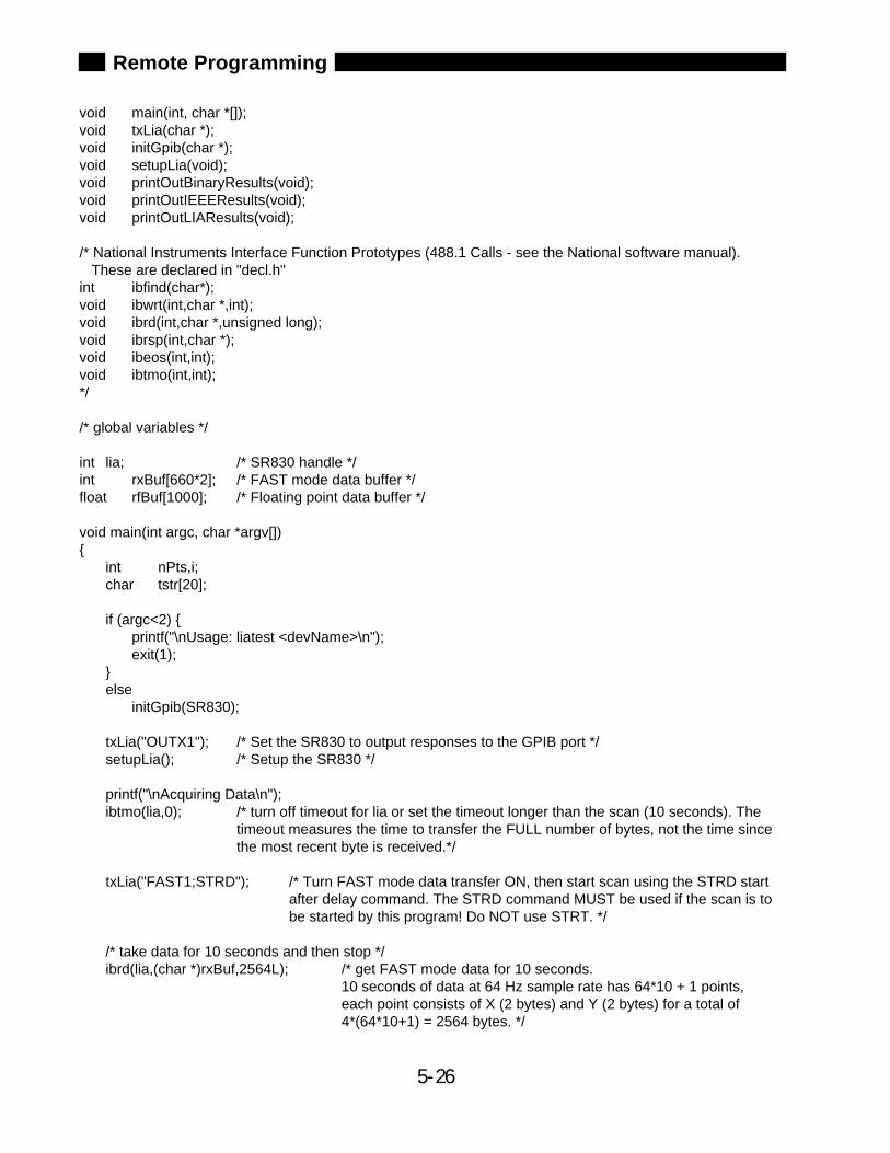
5-26
Remote Programming
void main(int, char *[]);void txLia(char *);void initGpib(char *);void setupLia(void);void printOutBinaryResults(void);void printOutIEEEResults(void);void printOutLIAResults(void);
/* National Instruments Interface Function Prototypes (488.1 Calls - see the National software manual). These are declared in "decl.h"int ibfind(char*);void ibwrt(int,char *,int);void ibrd(int,char *,unsigned long);void ibrsp(int,char *);void ibeos(int,int);void ibtmo(int,int);*/
/* global variables */
int lia; /* SR830 handle */int rxBuf[660*2]; /* FAST mode data buffer */float rfBuf[1000]; /* Floating point data buffer */
void main(int argc, char *argv[])
int nPts,i;char tstr[20];
if (argc<2) printf("\nUsage: liatest <devName>\n");exit(1);
else
initGpib(SR830);
txLia("OUTX1"); /* Set the SR830 to output responses to the GPIB port */setupLia(); /* Setup the SR830 */
printf("\nAcquiring Data\n");ibtmo(lia,0); /* turn off timeout for lia or set the timeout longer than the scan (10 seconds). The
timeout measures the time to transfer the FULL number of bytes, not the time sincethe most recent byte is received.*/
txLia("FAST1;STRD"); /* Turn FAST mode data transfer ON, then start scan using the STRD startafter delay command. The STRD command MUST be used if the scan is tobe started by this program! Do NOT use STRT. */
/* take data for 10 seconds and then stop */ibrd(lia,(char *)rxBuf,2564L); /* get FAST mode data for 10 seconds.
10 seconds of data at 64 Hz sample rate has 64*10 + 1 points, each point consists of X (2 bytes) and Y (2 bytes) for a total of 4*(64*10+1) = 2564 bytes. */
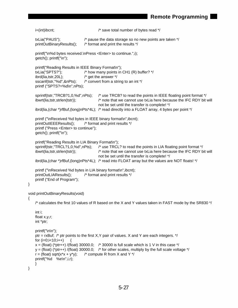
5-27
Remote Programming
i=(int)ibcnt; /* save total number of bytes read */
txLia("PAUS"); /* pause the data storage so no new points are taken */printOutBinaryResults(); /* format and print the results */
printf("\n%d bytes received.\nPress <Enter> to continue.",i);getch(); printf("\n");
printf("Reading Results in IEEE Binary Format\n");txLia("SPTS?"); /* how many points in CH1 (R) buffer? */ibrd(lia,tstr,20L); /* get the answer */sscanf(tstr,"%d",&nPts); /* convert from a string to an int */printf ("SPTS?=%d\n",nPts);
sprintf(tstr,"TRCB?1,0,%d",nPts); /* use TRCB? to read the points in IEEE floating point format */ibwrt(lia,tstr,strlen(tstr)); /* note that we cannot use txLia here because the IFC RDY bit will
not be set until the transfer is complete! */ibrd(lia,(char *)rfBuf,(long)nPts*4L); /* read directly into a FLOAT array, 4 bytes per point */
printf ("\nReceived %d bytes in IEEE binary format\n",ibcnt);printOutIEEEResults(); /* format and print results */printf ("Press <Enter> to continue");getch(); printf("\n");
printf("Reading Results in LIA Binary Format\n");sprintf(tstr,"TRCL?1,0,%d",nPts); /* use TRCL? to read the points in LIA floating point format */ibwrt(lia,tstr,strlen(tstr)); /* note that we cannot use txLia here because the IFC RDY bit will
not be set until the transfer is complete! */ibrd(lia,(char *)rfBuf,(long)nPts*4L); /* read into FLOAT array but the values are NOT floats! */
printf ("\nReceived %d bytes in LIA binary format\n",ibcnt);printOutLIAResults(); /* format and print results */printf ("End of Program");
void printOutBinaryResults(void)
/* calculates the first 10 values of R based on the X and Y values taken in FAST mode by the SR830 */
int i;float x,y,r;int *ptr;
printf("\n\n");ptr = rxBuf; /* ptr points to the first X,Y pair of values. X and Y are each integers. */for (i=0;i<10;i++) x = (float) (*ptr++) /(float) 30000.0; /* 30000 is full scale which is 1 V in this case */y = (float) (*ptr++) /(float) 30000.0; /* for other scales, multiply by the full scale voltage */r = (float) sqrt(x*x + y*y); /* compute R from X and Y */printf("%d %e\n",i,r);
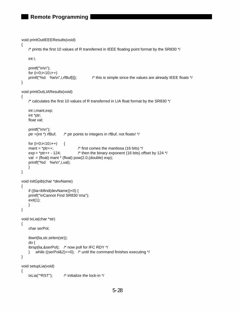
5-28
Remote Programming
void printOutIEEEResults(void)
/* prints the first 10 values of R transferred in IEEE floating point format by the SR830 */
int i;
printf("\n\n");for (i=0;i<10;i++)printf("%d %e\n",i,rfBuf[i]); /* this is simple since the values are already IEEE floats */
void printOutLIAResults(void)
/* calculates the first 10 values of R transferred in LIA float format by the SR830 */
int i,mant,exp;int *ptr;float val;
printf("\n\n");ptr =(int *) rfBuf; /* ptr points to integers in rfBuf, not floats! */
for (i=0;i<10;i++) mant = *ptr++; /* first comes the mantissa (16 bits) */exp = *ptr++ - 124; /* then the binary exponent (16 bits) offset by 124 */val = (float) mant * (float) pow(2.0,(double) exp);printf("%d %e\n",i,val);
void initGpib(char *devName)
if ((lia=ibfind(devName))<0) printf("\nCannot Find SR830 \n\a");exit(1);
void txLia(char *str)
char serPol;
ibwrt(lia,str,strlen(str));do ibrsp(lia,&serPol); /* now poll for IFC RDY */ while ((serPol&2)==0); /* until the command finishes executing */
void setupLia(void)
txLia("*RST"); /* initialize the lock-in */

5-29
Remote Programming
txLia("SRAT10; SEND0"); /* set 64 Hz sample rate, stop at end */txLia("DDEF1,1,0; DDEF2,1,0"); /* set CH1=R, CH2=theta. Buffers store CH1 and CH2 */
printf("Scan is Initialized, Press <Enter> to Begin Scan...");getch();

5-30
Remote Programming
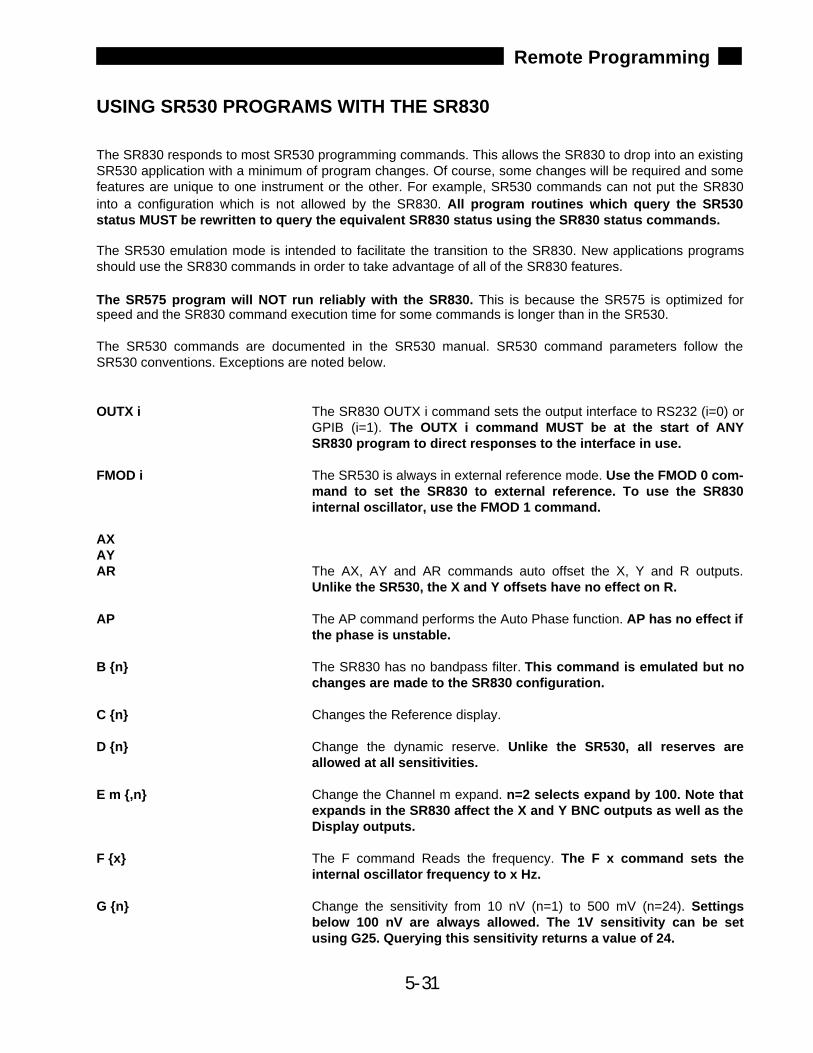
5-31
Remote Programming
USING SR530 PROGRAMS WITH THE SR830
The SR830 responds to most SR530 programming commands. This allows the SR830 to drop into an existingSR530 application with a minimum of program changes. Of course, some changes will be required and somefeatures are unique to one instrument or the other. For example, SR530 commands can not put the SR830into a configuration which is not allowed by the SR830. All program routines which query the SR530status MUST be rewritten to query the equivalent SR830 status using the SR830 status commands.
The SR530 emulation mode is intended to facilitate the transition to the SR830. New applications programsshould use the SR830 commands in order to take advantage of all of the SR830 features.
The SR575 program will NOT run reliably with the SR830. This is because the SR575 is optimized forspeed and the SR830 command execution time for some commands is longer than in the SR530.
The SR530 commands are documented in the SR530 manual. SR530 command parameters follow theSR530 conventions. Exceptions are noted below.
OUTX i The SR830 OUTX i command sets the output interface to RS232 (i=0) orGPIB (i=1). The OUTX i command MUST be at the start of ANYSR830 program to direct responses to the interface in use.
FMOD i The SR530 is always in external reference mode. Use the FMOD 0 com-mand to set the SR830 to external reference. To use the SR830internal oscillator, use the FMOD 1 command.
AXAYAR The AX, AY and AR commands auto offset the X, Y and R outputs.
Unlike the SR530, the X and Y offsets have no effect on R.
AP The AP command performs the Auto Phase function. AP has no effect ifthe phase is unstable.
B n The SR830 has no bandpass filter. This command is emulated but nochanges are made to the SR830 configuration.
C n Changes the Reference display.
D n Change the dynamic reserve. Unlike the SR530, all reserves areallowed at all sensitivities.
E m ,n Change the Channel m expand. n=2 selects expand by 100. Note thatexpands in the SR830 affect the X and Y BNC outputs as well as theDisplay outputs.
F x The F command Reads the frequency. The F x command sets theinternal oscillator frequency to x Hz.
G n Change the sensitivity from 10 nV (n=1) to 500 mV (n=24). Settingsbelow 100 nV are always allowed. The 1V sensitivity can be setusing G25. Querying this sensitivity returns a value of 24.
5-32
Remote Programming
H The SR830 does not sense the pre-amplifier. This command is emulat-ed and always returns 0.
I n Change the remote/local status. The SR830 Override Remote modecan override the I2 command. Use the OVRM command to changethis.
J Not implemented. Do not use.
K Not implemented. Do not use.
L m ,n Change the line notch filter status.
M n Change the reference mode to 2f. This command actually sets theharmonic detect number to n+1 in order to access harmonicshigher than 2f.
N m Change the noise bandwidth. This command has no effect on the timeconstants. If the S4 command is used to change the display toXnoise,Ynoise, then the N m command changes the effective ENBWwith which the output noise will be reported when queried using theQ1 or Q2 commands. The N command only affects the response toQ1 or Q2 and only if the S4 command is used first.
OX n ,vOY n ,vOR n ,v Change the X, Y or R offsets. Remember, v is an input voltage (not a
percentage) for the SR530. Unlike the SR530, the X and Y offsetshave no effect on R.
P v Change the reference phase shift. The value of v is limited to-360.0≤v≤729.99. The phase shift is also defined differently for theSR830. Check the sense of phase rotation if your application isphase sensitive.
Q1Q2QXQY Read the output values in Volts or degrees. When the current input is
selected, the outputs are returned in Amps.
R n Change the reference input mode.
S n Change the Output displays. The SR830 only responds if n=0 (X,Y),n=2 (R,θ) or n=4 (Xnoise,Ynoise).
T m ,n Change the time constant.
If m=1, then T1,n sets the time constant from 1 ms (n=1) to 30 ks(n=16). Time constants greater than 30 s are available only if thedetection frequency is below 200 Hz. The time constant slope is notchanged. The T1 query returns a maximum value of 11, even if thetime constant is greater than 100 s.
5-33
Remote Programming
If m=2:T2,0 changes the slope to 6 dB/oct, time constant not changed.T2,1 changes the time constant to 100 ms with 12 dB/oct slope.T2,2 changes the time constant to 1 s with 12 dB/oct slope.
Use the T2,n command to change the filter slope, then use T1,n toselect the time constant.
U m ,n Not implemented. Do not use.
V n Change the value of the SRQ mask. This command changes the serialpoll enable register of the SR830. The serial poll byte is that of theSR830 not the SR530! Programs which query the SR530 status needto be changed to query the equivalent SR830 status byte.
W n Not implemented. Do not use.
X n ,v Set or query the auxiliary analog ports. If n=1,2,3 or 4, the value of AuxInput n is returned. If n=5 or 6, then the Xn,v sets the value of AuxOutput 1 or 2 to v Volts. The X5 ratio is NOT implemented. Ratio out-puts must be done using the SR830 display ratio mode.
Y n Not implemented. Do not use. Use the SR830 status commands toread the SR830 status bytes.
Z Reset the SR830. The instrument is reset to the SR830 default setuplisted in the Operation section. This differs slightly from the SR530default. (The sensitivity is set to 1 V, not 500 mV).

5-34
Remote Programming
PERFORMANCE TESTS
Introduction The performance tests described in this section are designed to verifywith a high degree of confidence that the unit is performing correctly.
The results of each test may be recorded on the test sheet at the end ofthis section.
Serial Number If you need to contact Stanford Research Systems, please have theserial number of your unit available. The 5-digit serial number is printedon a label affixed to the rear panel. The serial number is also displayedon the CH1 and CH2 displays when the unit is powered on.
Firmware Revision The firmware revision code is shown on the Reference display when theunit is powered on.
Preset Throughout this section, it will be necessary to preset the lock-in into aknown default state. To do this, turn the power off. Turn the power backon while holding down the [Setup] key. The unit will perform power uptests and then assume the default settings. Each test generally startswith a preset. This procedure will be referred to as PRESET.
Warm Up The lock-in should be turned on and allowed to warm up for at least anhour before any tests are performed. The self test does not require anywarm up period.
It is necessary to turn the unit off and on to preset it. As long as the unitis powered on immediately, this will not affect the test results.
Test Record Make a copy of the SR830 Performance Test Record at the end of thissection. Fill in the results of the tests on this record. This record will allowyou to determine whether the tests pass or fail and also to preserve arecord of the tests.
If A Test Fails If a test fails, you should check the settings and connections of any exter-nal equipment and, if possible, verify its operation using a DVM, scope orsome other piece of test equipment.
After checking the setup, repeat the test from the beginning to make surethat the test was performed correctly.
If the test continues to fail, contact Stanford Research Systems for fur-ther instructions. Make sure that you have the unit's serial number andfirmware revision code handy. Have the test record on hand as well.
Necessary Equipment The following equipment is necessary to complete the performance tests.The suggested equipment or its equivalent should be used.
1. Frequency SynthesizerFreq Range 1 Hz to 1 MHzFreq Accuracy better than 5 ppmAmplitude Accuracy 0.2 dB from 1 Hz to 100 kHzHarmonic Distortion ≤ -65 dBc
6-1
6-2
Performance Tests
Spurious ≤ -55 dBcTTL SYNC available
Recommended SRS DS335
2. AC CalibratorFreq Range 10 Hz to 100 kHzAmplitude 1 mV to 10 VAccuracy 0.1%External phase locking capability
Recommended Fluke 5200A
3. DC VoltmeterRange 19.999 V, 4 1/2 digitsAccuracy 0.005%
Recommended Fluke 8840A
4. Feedthrough TerminationsImpedance 50 Ω
Front Panel Display Test To test the front panel displays, press the [Phase] and [Freq] keystogether. All of the LED's will turn on. Press [Phase] to decrease thenumber of on LED's to half on, a single LED and no LED's on. Use theknob to move the turned on LED's across the panel. Press [Freq] toincrease the number of on LED's. Make sure that every LED can beturned on. Press any other key to exit this test mode.
Keypad Test To test the keypad, press the [Phase] and [Ampl] keys together. TheCH1 and CH2 displays will read 'Pad code' and a number of LED indica-tors will be turned on. The LED's indicate which keys have not beenpressed yet. Press all of the keys on the front panel, one at a time. Aseach key is pressed, the key code is displayed in the Reference display,and nearest indicator LED turns off. When all of the keys have beenpressed, the display will return to normal. To return to normal operationwithout pressing all of the keys, simply turn the knob.
6-3
Performance Tests
1. Self TestsThe self tests check the lock-in hardware. These are functional tests and do not relate to the specifications.These tests should be checked before any of the performance tests.
Setup
No external setup is required for this test.
Procedure
1) PRESET (Turn on the lock-in with the [Setup] key pressed)Check the results of the DATA, BATT, PROG and DSP tests.
2) This completes the functional hardware tests. Enter the results of this test in the test record at the endof this section.

6-4
Performance Tests
6-5
Performance Tests
2. DC OffsetThis test measures the DC offset of the input.
Setup
Connect a 50Ω terminator to the A input. This shorts the input so the lock-in's own DC offset will bemeasured.
Procedure
1) PRESET (Turn the lock-in off and on with the [Setup] key pressed)
2) Press the keys in the following sequence:
[Freq]Use the knob to set the frequency to 1.00 Hz.
[Sensitivity Down]Set the sensitivity to 1 mV.
[CH1 Display]Set the Channel 1 display to R.
3) Wait at least 10 seconds, then record the reading of R.
4) Press
[Couple]Select DC coupling.
5) Wait 10 seconds, then record the reading of R.
6) This completes the DC offset test. Enter the results of this test in the test record at the end of thissection.

6-6
Performance Tests
6-7
Performance Tests
3. Common Mode RejectionThis test measures the common mode rejection of the lock-in.
Setup
We will use the internal oscillator sine output to provide the signal.
Connect the Sine Out to both the A and B inputs of the lock-in. Use equal length cables from A and B to aBNC TEE. Connect the cable from the Sine Out to the TEE. Do not use any termination.
Procedure
1) PRESET (Turn the lock-in off and on with the [Setup] key pressed)
2) Press the keys in the following sequence:
[Freq]Use the knob to adjust the frequency to 100.0 Hz.
[Channel 1 Display]Set the Channel 1 display to R.
3) The value of R should be 1.000 V (within 2%).
4) Press
[Couple]Select DC coupling.
[Input]Select A-B.
[Sensitivity Down]Set the sensitivity to 200 µV.
5) Record the value of R.
6) This completes the CMRR measurement test. The common mode rejection is 20log(1.0/R) where R isin Volts. Enter the results of this test in the test record at the end of this section.

6-8
Performance Tests
6-9
Performance Tests
4. Amplitude Accuracy and FlatnessThis test measures the amplitude accuracy and frequency response.
Setup
We will use the frequency synthesizer to provide an accurate frequency and the AC calibrator to provide asine wave with an exact amplitude.
Connect the output of the frequency synthesizer to the phase lock input of the calibrator. Connect the outputof the AC calibrator to the A input of the lock-in. Be sure to use the appropriate terminations where required.Connect the TTL SYNC output of the synthesizer to the Reference Input of the lock-in.
Set the Synthesizer to: Set the AC Calibrator to:Function Sine Frequency 1 kHzFrequency 1 kHz Amplitude 1.000 VrmsAmplitude 0.5 Vrms Voltage OffOffset off or 0V Phase Lock OnSweep off Sense InternalModulation none
Procedure
1) PRESET (Turn the lock-in off and on with the [Setup] key pressed)
2) Press the keys in the following sequence:
[Source]Select External reference mode (INTERNAL led off).
[Trig]Select POS EDGE.
[Channel 1 Display]Set the Channel 1 display to R.
[Slope/Oct]Select 24 dB/oct.
3) Amplitude accuracy is verified at 1 kHz and various sensitivities. For each sensitivity setting in thetable below, perform steps 3a through 3c.
Sensitivity AC Calibrator Amplitude1 V 1.0000 Vrms
200 mV 200.00 mVrms100 mV 100.000 mVrms20 mV 20.000 mVrms10 mV 10.000 mVrms
a) Set the AC calibrator to the amplitude shown in the table.
6-10
Performance Tests
b) Press [Sensitivity Up/Dn]
Select the sensitivity from the table.
c) Wait for the R reading to stabilize. Record the value of R for each sensitivity.
4) Frequency response is checked at frequencies above 1 kHz. The test frequencies are listed below. Test Frequencies
24 kHz48 kHz72 kHz96 kHz
a) Set the AC calibrator to 1 kHz and an amplitude of 200.00 mVrms.
b) Set the frequency synthesizer to 1 kHz.
c) Press[Sensitivity Up/Dn]
Set the sensitivity 200 mV.
d) Set the AC calibrator and frequency synthesizer to the frequency in the table.
e) Wait for the R reading to stabilize. Record the value of R.
f) Repeat steps 4d and 4e for all of the frequencies listed.
5) This completes the amplitude accuracy and frequency response test. Enter the results of this test inthe test record at the end of this section.
6-11
Performance Tests
5. Amplitude LinearityThis test measures the amplitude linearity. This tests how accurately the lock-in measures a signal smallerthan full scale.
Setup
We will use the frequency synthesizer to provide an accurate frequency and the AC calibrator to provide asine wave with an exact amplitude.
Connect the output of the frequency synthesizer to the phase lock input of the calibrator. Connect the outputof the AC calibrator to the A input of the lock-in. Be sure to use the appropriate terminations where required.Connect the TTL SYNC output of the synthesizer to the Reference Input of the lock-in.
Set the Synthesizer to: Set the AC Calibrator to:Function Sine Frequency 1 kHzFrequency 1 kHz Amplitude 1.0000 VrmsAmplitude 0.5 Vrms Voltage OffOffset off or 0V Phase Lock OnSweep off Sense InternalModulation none
Procedure
1) PRESET (Turn the lock-in off and on with the [Setup] key pressed)
2) Press the keys in the following sequence:
[Source]Select External reference mode (INTERNAL led off).
[Trig]Select POS EDGE.
[Channel 1 Display]Set the Channel 1 display to R.
[Slope/Oct]Select 24 dB/oct.
3) For each of the amplitudes listed below, perform steps 3a through 3c.
AC Calibrator Amplitudes1.0000 Vrms
100.00 mVrms10.000 mVrms
a) Set the AC calibrator to the amplitude in the table.
b) Wait for the R reading to stabilize. Record the value of R.
4) This completes the amplitude linearity test. Enter the results of this test in the test record at the end ofthis section.

6-12
Performance Tests
6-13
Performance Tests
6. Frequency AccuracyThis test measures the frequency accuracy of the lock-in. This tests the accuracy of the frequency counterinside the unit. The counter is used only in external reference mode. The internal oscillator frequency is set bya crystal and has 25 ppm frequency accuracy.
Setup
We will use the frequency synthesizer to provide the reference signal.
Connect the TTL SYNC output of the frequency synthesizer to the Reference input of the lock-in.
Procedure
1) PRESET (Turn the lock-in off and on with the [Setup] key pressed)
2) Set the frequency synthesizer to a frequency of 10 kHz.
3) Press the keys in the following sequence:
[Source]Select External reference mode (INTERNAL led off).
[Trig]Select POS EDGE.
4) The lock-in should be locked to the external reference. The frequency is displayed at the bottom ofthe screen. Record the frequency reading.
5) This completes the frequency accuracy test. Enter the results of this test in the test record at the endof this section.

6-14
Performance Tests
6-15
Performance Tests
7. Phase AccuracyThis test measures the phase accuracy of the lock-in. Due to the design of the lock-in, the phase accuracycan be determined by measuring the phase of the internal oscillator Sine Out.
Setup
Connect the Sine Out to the A input of the lock-in using a 1 meter BNC cable. Do not use any termination.
Procedure
1) PRESET (Turn the lock-in off and on with the [Setup] key pressed)
2) Press the keys in the following sequence:
[Slope /Oct]Select 24 dB/oct.
[Couple]Select DC coupling.
[Channel 1 Display]Set the Channel 1 display to R.
[Channel 2 Display]Set the Channel 2 display to θ.
3) The value of R should be 1.000 V (±2%) and the value of θ should 0° (±1°).
4) Phase accuracy is checked at various frequencies. The test frequencies are listed below.
Test Frequencies10 Hz
100 Hz1 kHz10 kHz
a) Press
[Freq]Use the knob to set the internal oscillator to the frequency from the table.
b) Wait for the readings to stabilize. Record the value of θ.
c) Repeat steps 4a and 4b for all frequencies in the table.
5) This completes the phase accuracy test. Enter the results of this test in the test record at the end ofthis section.

6-16
Performance Tests
6-17
Performance Tests
8. Sine Output Amplitude Accuracy and FlatnessThis test measures the amplitude accuracy and frequency response of the internal oscillator Sine Out.
Setup
We will use the lock-in to measure the Sine Out. Connect the Sine Out to the A input of the lock-in.
Procedure
1) PRESET (Turn the lock-in off and on with the [Setup] key pressed)
2) Press the keys in the following sequence:
[Channel 1 Display]Set the Channel 1 display to R.
3) Amplitude accuracy is verified at 1 kHz using various sensitivities. For each sine amplitude and sensi-tivity setting in the table below, perform steps 3a through 3b.
Sensitivity Sine Output Amplitude1 V 1.000 Vrms
200 mV 0.200 Vrms50 mV 0.050 Vrms10 mV 0.010 Vrms
a) Press [Ampl]
Use the knob to set the sine amplitude to the value in the table.
[Sensitivity Up/Dn]Set the sensitivity to the value in the table.
b) Wait for the R reading to stabilize. Record the value of R.
c) Repeat 3a and 3b for each amplitude in the table.
4) Frequency response is checked at frequencies above 1 kHz. The sine amplitude is set to 1 Vrms forall frequencies. The test frequencies are listed below.
Test Frequencies24 kHz48 kHz72 kHz96 kHz
c) Press[Sensitivity Up]
Set the sensitivity to 1 V.
[Ampl]Use the knob to set the sine amplitude to 1.00 V.
6-18
Performance Tests
d) Press[Freq]
Use the knob to set the internal oscillator frequency to the value in the table.
e) Wait for the R reading to stabilize. Record the value of R.
f) Repeat steps 4d and 4e for all of the frequencies listed.
5) This completes the sine output amplitude accuracy and frequency response test. Enter the results ofthis test in the test record at the end of this section.
6-19
Performance Tests
9. DC Outputs and InputsThis test measures the DC accuracy of the DC outputs and inputs of the lock-in.
Setup
We will use the digital voltmeter (DVM) to measure the DC outputs of the lock-in. Then we will use one of theoutputs to generate a voltage to measure on the DC inputs.
Connect a 50Ω termination to the A input.
Procedure
1) PRESET (Turn the lock-in off and on with the [Setup] key pressed)
2) For the CH1 and CH2 outputs, repeat steps 2a through 2e.
a) Connect the CH1 (or CH2) output to the DVM. Set the DVM to 19.999 V range.
b) Press[Channel 1 (or 2) Offset On/Off]
Turn the offset on.
c) For each of the offsets in the table below, repeat steps 2d and 2e.
Offsets (%)-100.00-50.000.00
50.00100.00
d) Press[Channel 1 (or 2) Offset Modify]
Show the offset in the Reference display.Use the knob to set the offset to the value in the table.
e) Record the DVM reading.
3) For each Aux Output (1, 2, 3 and 4), repeat steps 3a through 3e.
a) Press[Aux Out]
Display the correct Aux Output level on the Reference display.
b) Connect the selected Aux Output (on the rear panel) to the DVM.
6-20
Performance Tests
c) For each output voltage in the table below, repeat steps 3d and 3e.
Output Voltages-10.000-5.0000.0005.000
10.000
d) Use the knob to adjust the Aux Output level to the value from the table.
e) Record the DVM reading.
4) Press
[Aux Out]Display Aux Out 1 on the Reference display.
5) For Aux Inputs 1 and 2, repeat steps 5a through 5e.
a) Connect Aux Out 1 to Aux Input 1 (or 2) with a BNC cable.
b) Press[Channel 1 Display]
Set the Channel 1 display to AUX IN 1 (or 2)
c) For each output voltage in table 3c above, repeat steps 5d and 5e.
d) Use the knob to adjust the Aux Out 1 level to the values from the table above.
e) Record the Aux Input 1 (or 2) value from the Channel 1 display.
6) For Aux Inputs 3 and 4, repeat steps 6a through 6e.
a) Connect Aux Out 1 to Aux Input 3 (or 4) with a BNC cable.
b) Press[Channel 2 Display]
Set the Channel 2 display to AUX IN 3 (or 4)
c) For each output voltage in table 3c above, repeat steps 6d and 6e.
d) Use the knob to adjust the Aux Out 1 level to the values from the table above.
e) Record the Aux Input 3 (or 4) value from the Channel 1 display.
7) This completes the DC outputs and inputs test. Enter the results of this test in the test record at theend of this section.
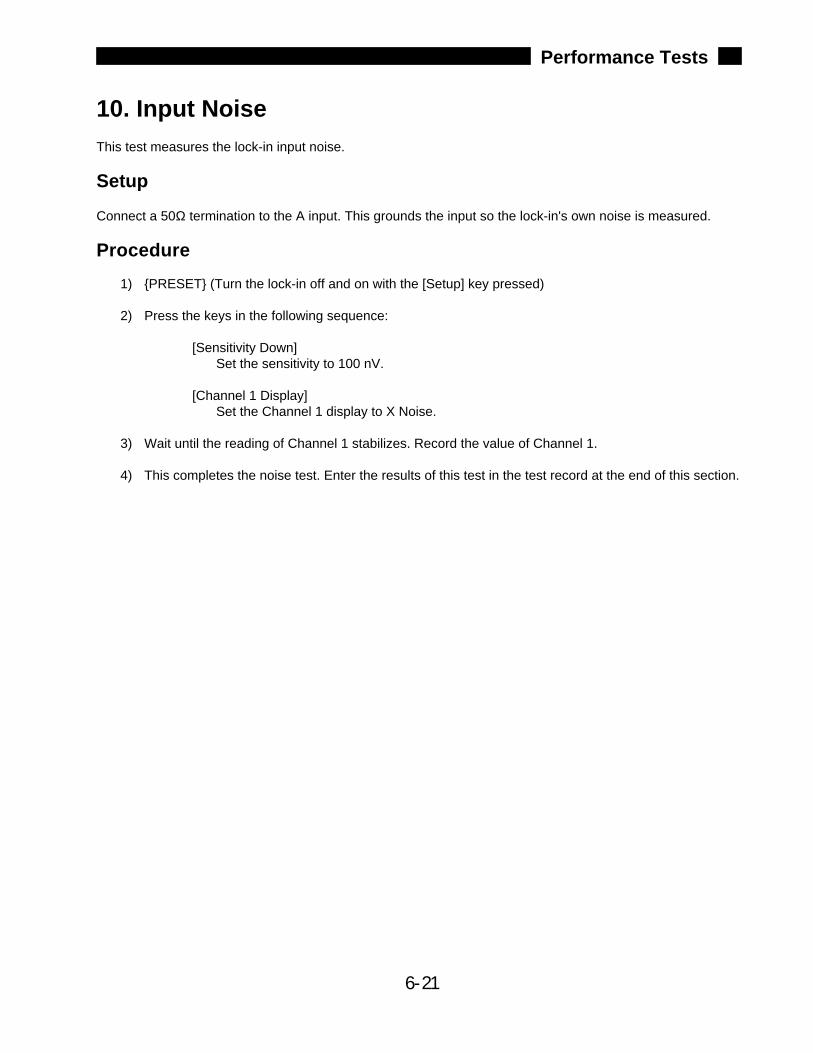
6-21
Performance Tests
10. Input NoiseThis test measures the lock-in input noise.
Setup
Connect a 50Ω termination to the A input. This grounds the input so the lock-in's own noise is measured.
Procedure
1) PRESET (Turn the lock-in off and on with the [Setup] key pressed)
2) Press the keys in the following sequence:
[Sensitivity Down]Set the sensitivity to 100 nV.
[Channel 1 Display]Set the Channel 1 display to X Noise.
3) Wait until the reading of Channel 1 stabilizes. Record the value of Channel 1.
4) This completes the noise test. Enter the results of this test in the test record at the end of this section.

6-22
Performance Tests
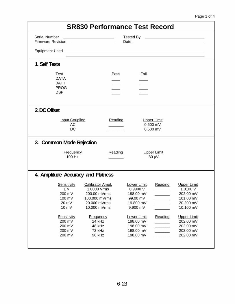
SR830 Performance Test Record Serial Number Tested ByFirmware Revision Date
Equipment Used
1. Self Tests
Test Pass FailDATA ____ ____BATT ____ ____PROG ____ ____DSP ____ ____
2. DC Offset
Input Coupling Reading Upper LimitAC _______ 0.500 mVDC _______ 0.500 mV
3. Common Mode Rejection
Frequency Reading Upper Limit100 Hz _______ 30 µV
4. Amplitude Accuracy and Flatness
Sensitivity Calibrator Ampl. Lower Limit Reading Upper Limit1 V 1.0000 Vrms 0.9900 V _______ 1.0100 V
200 mV 200.00 mVrms 198.00 mV _______ 202.00 mV100 mV 100.000 mVrms 99.00 mV _______ 101.00 mV20 mV 20.000 mVrms 19.800 mV _______ 20.200 mV10 mV 10.000 mVrms 9.900 mV _______ 10.100 mV
Sensitivity Frequency Lower Limit Reading Upper Limit200 mV 24 kHz 198.00 mV _______ 202.00 mV200 mV 48 kHz 198.00 mV _______ 202.00 mV200 mV 72 kHz 198.00 mV _______ 202.00 mV200 mV 96 kHz 198.00 mV _______ 202.00 mV
6-23
Page 1 of 4
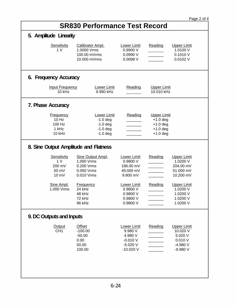
SR830 Performance Test Record 5. Amplitude Linearity
Sensitivity Calibrator Ampl. Lower Limit Reading Upper Limit1 V 1.0000 Vrms 0.9900 V _______ 1.0100 V
100.00 mVrms 0.0990 V _______ 0.1010 V10.000 mVrms 0.0098 V _______ 0.0102 V
6. Frequency Accuracy
Input Frequency Lower Limit Reading Upper Limit10 kHz 9.990 kHz _______ 10.010 kHz
7. Phase Accuracy
Frequency Lower Limit Reading Upper Limit10 Hz -1.0 deg _______ +1.0 deg
100 Hz -1.0 deg _______ +1.0 deg1 kHz -1.0 deg _______ +1.0 deg10 kHz -1.0 deg _______ +1.0 deg
8. Sine Output Amplitude and Flatness
Sensitivity Sine Output Ampl. Lower Limit Reading Upper Limit1 V 1.000 Vrms 0.9800 V _______ 1.0200 V
200 mV 0.200 Vrms 196.00 mV _______ 204.00 mV50 mV 0.050 Vrms 49.000 mV _______ 51.000 mV10 mV 0.010 Vrms 9.800 mV _______ 10.200 mV
Sine Ampl. Frequency Lower Limit Reading Upper Limit1.000 Vrms 24 kHz 0.9800 V _______ 1.0200 V
48 kHz 0.9800 V _______ 1.0200 V72 kHz 0.9800 V _______ 1.0200 V96 kHz 0.9800 V _______ 1.0200 V
9. DC Outputs and Inputs
Output Offset Lower Limit Reading Upper LimitCH1 -100.00 9.980 V _______ 10.020 V
-50.00 4.980 V _______ 5.020 V0.00 -0.010 V _______ 0.010 V50.00 -5.020 V _______ -4.980 V100.00 -10.020 V _______ -9.980 V
Page 2 of 4
6-24
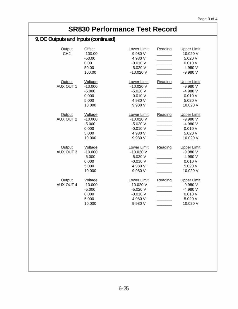
SR830 Performance Test Record 9. DC Outputs and Inputs (continued)
Output Offset Lower Limit Reading Upper LimitCH2 -100.00 9.980 V _______ 10.020 V
-50.00 4.980 V _______ 5.020 V0.00 -0.010 V _______ 0.010 V50.00 -5.020 V _______ -4.980 V100.00 -10.020 V _______ -9.980 V
Output Voltage Lower Limit Reading Upper LimitAUX OUT 1 -10.000 -10.020 V _______ -9.980 V
-5.000 -5.020 V _______ -4.980 V0.000 -0.010 V _______ 0.010 V5.000 4.980 V _______ 5.020 V10.000 9.980 V _______ 10.020 V
Output Voltage Lower Limit Reading Upper LimitAUX OUT 2 -10.000 -10.020 V _______ -9.980 V
-5.000 -5.020 V _______ -4.980 V0.000 -0.010 V _______ 0.010 V5.000 4.980 V _______ 5.020 V10.000 9.980 V _______ 10.020 V
Output Voltage Lower Limit Reading Upper LimitAUX OUT 3 -10.000 -10.020 V _______ -9.980 V
-5.000 -5.020 V _______ -4.980 V0.000 -0.010 V _______ 0.010 V5.000 4.980 V _______ 5.020 V10.000 9.980 V _______ 10.020 V
Output Voltage Lower Limit Reading Upper LimitAUX OUT 4 -10.000 -10.020 V _______ -9.980 V
-5.000 -5.020 V _______ -4.980 V0.000 -0.010 V _______ 0.010 V5.000 4.980 V _______ 5.020 V10.000 9.980 V _______ 10.020 V
Page 3 of 4
6-25
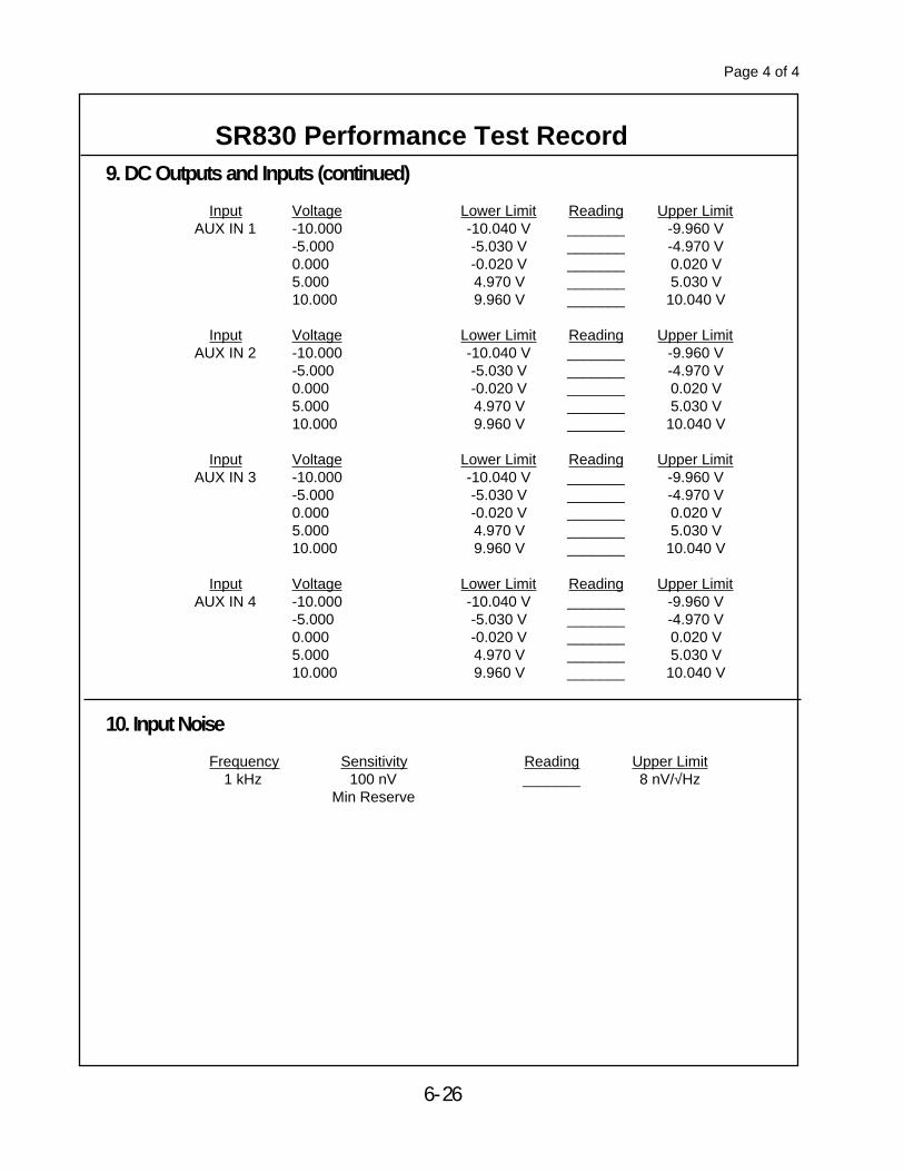
SR830 Performance Test Record 9. DC Outputs and Inputs (continued)
Input Voltage Lower Limit Reading Upper LimitAUX IN 1 -10.000 -10.040 V _______ -9.960 V
-5.000 -5.030 V _______ -4.970 V0.000 -0.020 V _______ 0.020 V5.000 4.970 V _______ 5.030 V10.000 9.960 V _______ 10.040 V
Input Voltage Lower Limit Reading Upper LimitAUX IN 2 -10.000 -10.040 V _______ -9.960 V
-5.000 -5.030 V _______ -4.970 V0.000 -0.020 V _______ 0.020 V5.000 4.970 V _______ 5.030 V10.000 9.960 V _______ 10.040 V
Input Voltage Lower Limit Reading Upper LimitAUX IN 3 -10.000 -10.040 V _______ -9.960 V
-5.000 -5.030 V _______ -4.970 V0.000 -0.020 V _______ 0.020 V5.000 4.970 V _______ 5.030 V10.000 9.960 V _______ 10.040 V
Input Voltage Lower Limit Reading Upper LimitAUX IN 4 -10.000 -10.040 V _______ -9.960 V
-5.000 -5.030 V _______ -4.970 V0.000 -0.020 V _______ 0.020 V5.000 4.970 V _______ 5.030 V10.000 9.960 V _______ 10.040 V
10. Input Noise
Frequency Sensitivity Reading Upper Limit1 kHz 100 nV _______ 8 nV/√Hz
Min Reserve
Page 4 of 4
6-26
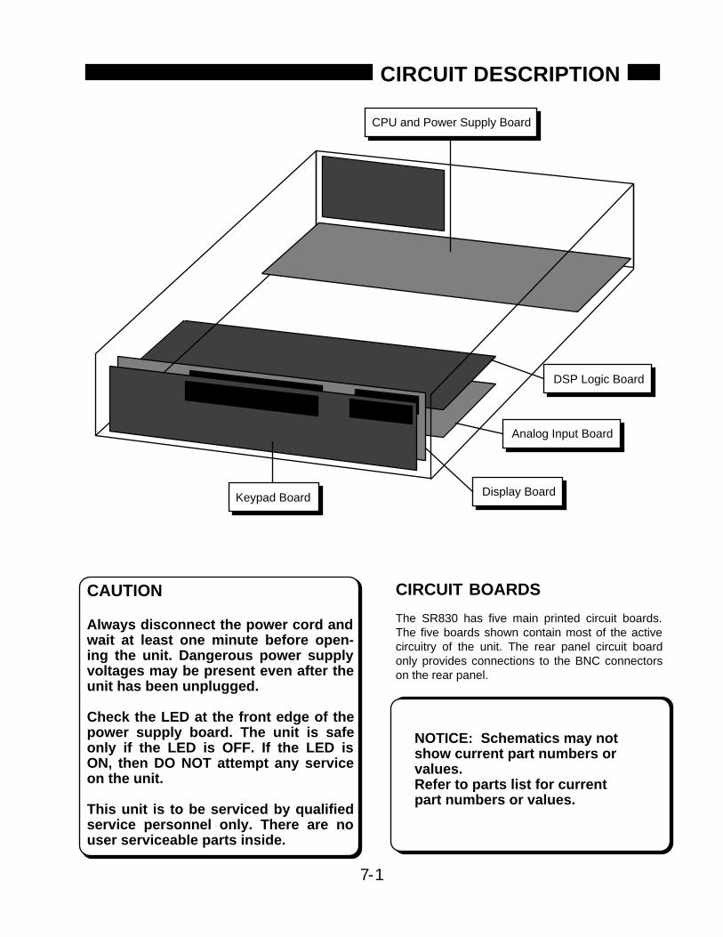
CAUTION
Always disconnect the power cord andwait at least one minute before open-ing the unit. Dangerous power supplyvoltages may be present even after theunit has been unplugged.
Check the LED at the front edge of thepower supply board. The unit is safeonly if the LED is OFF. If the LED isON, then DO NOT attempt any serviceon the unit.
This unit is to be serviced by qualifiedservice personnel only. There are nouser serviceable parts inside.
CIRCUIT BOARDS
The SR830 has five main printed circuit boards.The five boards shown contain most of the activecircuitry of the unit. The rear panel circuit boardonly provides connections to the BNC connectorson the rear panel.
7-1
CIRCUIT DESCRIPTION
CPU and Power Supply Board
DSP Logic Board
Analog Input Board
Keypad Board Display Board
NOTICE: Schematics may notshow current part numbers orvalues. Refer to parts list for currentpart numbers or values.

7-2
Circuit Description
7-3
Circuit Description
The CPU board contains the microprocessorsystem. All display, front panel, disk, and comput-er interfaces are on this board.
MICROPROCESSOR SYSTEM
The microprocessor, U101, is an 80C186 micro-controller which integrates a fast 16 bit processor,counter-timers, interrupt controller, DMA controller,and I/O decoding into a single component.
The 80C186 uses a 24.00 MHz crystal, X101, asits oscillator. The instruction clock cycle is 2 oscil-lator cycles or 12.0 MHz. The data and lower 16bits of address are multiplexed on AD0-AD15.U201, U202, U203 latch the address A0-A19 atthe beginning of each memory or I/O cycle. U204and U205 are bidirectional data bus drivers whichare active during the data read/write portion ofeach memory or I/O cycle.
The 80C186 can address 1 Mbyte of memory and64k of I/O space. The memory is mapped into 2256kbyte blocks. Each block has 2 sockets, onefor the low byte and one for the high byte of data.
U303 and U304 are 128kbyte EPROMS holdingthe program boot firmware. This memory ismapped at C0000H to FFFFFH (256k).
U401 and U402 are 128kbyte CMOS static RAMsmapped at 00000H to 3FFFFH (256k). U401 andU402 are backed up by the battery. Q401 providespower down RAM protection. This memory issystem memory.
3 of the 7 80C186's peripheral chip select strobesare used by peripherals on the CPU board. -PCS0is decoded into 16 I/O strobes which access thedisplays, keypad and knob, etc. -PCS1 decodesthe the GPIB controller. -PCS2 selects the UART.
FRONT PANEL INTERFACE
U614 and U615 buffer the front panel connectorcable. The Display Board holds the front panellogic.
SPIN KNOB
The knob is an optical encoder buffered by U612.Each transition of its outputs is clocked into U610or U611 and generates an interrupt at the outputof U602A. The processor keeps track of the knob'sposition continuously.
SPEAKER
The speaker is driven by a timer on the 80C186.The timer outputs a square wave which is enabledby U602B and drives the speaker through Q705.
GPIB INTERFACE
The GPIB (IEEE-488) interface is provided byU902, a TMS9914A controller. U903 and U904buffer data I/O to the GPIB connector. U902 is pro-grammed to provide an interrupt to the processorwhenever there is bus activity addressed to theunit.
RS232 INTERFACE
The SCN2641 UART, U905, provides all of theUART functions as well as baud rate generation.Standard baud rates up to 19.2k can be generatedfrom the 3.6864 MHz clock. U906 buffers the out-going data and control signals. Incoming signalsare received by U705A and U705B. If the hostcomputer asserts DTR, RS232 data output fromthe unit will cease.
The RS232 port is a DCE and may be connectedto a PC using a standard serial cable (not a "nullmodem" cable).
EXPANSION CONNECTOR
All control of the data acquisition hardware isthrough the signals on the 30 pin expansionconnector.
CPU and POWER SUPPLY BOARD
7-4
Circuit Description
POWER SUPPLY
CAUTION: Dangerous voltages are present onthis circuit board whenever the instrument isattached to an AC power source and the rearpanel power switch is "on".
Always disconnect the power cord and wait atleast one minute before opening the unit.Check the LED at the front edge of the powersupply board. The unit is safe only if the LED isOFF. If the LED is ON, then DO NOT attemptany service on the unit.
UNREGULATED POWER SUPPLIES
A power entry module, with RF line filter, is usedto configure the unit for 100, 120, 220, or 240VAC. The line filter reduces noise from the instru-ment and reduces the unit's susceptibility to linevoltage noise.
Bridge rectifiers are used to provide unregulatedDC at ±24V, ±20V and ±8V. Schottky diodes areused for all supplies to reduce rectifier losses.
Resistors provide a bleed current on all of theunregulated supply filter capacitors. Because ofthe large capacitances in this circuit, the time forthe voltages to bleed to zero is about a minuteafter the power is turned off.
POWER SUPPLY REGULATORS
The voltage regulators provide outputs at +5V,-5V, ±15V, and ±12V. The +5V regulators aredesigned to operate with a very low drop-outvoltage.
There are 2 +5V supplies, one to power the CPUboard and front panel displays (+5V_P), and oneto power the DSP Logic Board (+5V_I).
U6 and U8 are the ±12V regulators. U5 is the -5Vregulator.
U9 and U10 provide ±20V sources which are notreferenced to the digital ground (as are all of thesupplies mentioned above). This allows the analoginput board to establish a ground at the signalinput without digital ground noise.
U1 provides power-up and power-down reset.
The 24 VDC brushless fan cools the heat sink andpower supply rectifiers.
7-5
Circuit Description
OVERVIEW
The DSP LOGIC BOARD takes a digital input fromthe A/D Converter on the Analog Input Board andperforms all of the computations related to themeasurement before it is displayed on the screen.This includes generating the digital reference sinewave, demodulating the signal, low-pass filteringthe results, and offset and expanding the outputs.The internal oscillator sine output and Aux D/Aoutputs are generated on this board as well. Thereference phase lock loop controls the clock of thisboard whenever the reference mode is external.These functions are implemented within a systemcomprised of five functional blocks: the DigitalSignal Processor (DSP), the DAC Outputs, theTiming Signal Generator, the Reference ClockGenerator and the I/O Interface. Through the useof highly efficient algorithms, the system is capa-ble of real-time lock-in operation to 100 kHz with24 dB/oct filtering on both X and Y as well as pro-viding a synthesized analog sine output.
DSP PROCESSOR
The SR830 utilizes a Motorola 24-bit DSP56001digital signal processor (U501). The DSP is config-ured without external memory. The lock-in algo-rithms run entirely within the internal program anddata memory of the DSP itself. The Host proces-sor bus is connected to the main CPU Board viathe I/O Interface on the DSP Logic Board. The80C186 processor on the CPU Board acts as the"host" processor to the DSP. DSP firmware andcommands are downloaded from the CPU Boardto invoke different operating modes. The DSP alsohas two dedicated serial ports: one for receiving,and one for transmitting.
REFERENCE CLOCK SOURCE
The clock to the DSP is derived from the timinggenerator. U120, U121 and U122 are gates whichselect the clock source for the entire digital board.
When the reference mode is internal, the30.208 MHz crystal (U111) is used. The A/Dinputs and D/A outputs run with a 256 kHz cycleand the DSP performs 59 instructions each cycle(each instruction takes two clocks). The crystal
also sets the internal reference frequencyaccuracy.
When the reference mode is external, the VCO(voltage controlled oscillator, U110) is used as thesystem clock. The VCO nominally runs at 30 MHzas well. U105 is a phase comparator. The externalreference input, discriminated by U103 (or TTLbuffered through U104D) is one of the inputs tothe phase comparator. The other input is the inter-nal reference. The DSP always synthesizes a sinewave at the reference frequency. This is the SineOutput. This sine output is discriminated by U209into a TTL square wave (TTL Sync Out) and is theother input to the phase comparator. The phaselock loop then controls the VCO which is the clockto the DSP. This in turn changes the sine outputfrequency to maintain frequency lock with theexternal reference. The DSP is constantly gettingexternal frequency information from the host(based upon counter U622) which allows the DSPto synthesize nearly the correct reference frequen-cy assuming a 30 MHz clock. This keeps the VCOwithin range at all frequencies.
TIMING GENERATOR
All timing signals for the DSP and Analog boardsare derived from the system clock by PALs (U601-604). These PALs generate the clocks for theDACs and A/D converter, the multiplexing signalsfor the Aux inputs and outputs, etc.
SERIAL CHANNELS
There are two serial data streams from the A/Dconverter on the Analog Input board which need tobe received by the DSP. The digitized input signalis received directly via the DSP's serial input port.The Aux A/D input data is shifted into a pair ofserial-to-parallel registers (U502 and U503) and isread via the DSP data bus. Each A/D input chan-nel provides a new sample every 4 µs.
There are two dual-channel D/A converters on thisboard for a total of four D/A output channels. Eachoutput channel provides a new output every 4 µs.This means that 4 output values must be writtenby the DSP each 4 µs cycle. The DSP writes toone channel of each D/A converter via its serial
DSP LOGIC BOARD
7-6
Circuit Description
transmit port each cycle. The transmit port oper-ates at twice the frequency of the receive port. TheDSP writes to the other channel of each DAC via apair of parallel-to-serial registers (U504 andU505).
DAC OUTPUTS
Three of the DAC output channels provide SineOut, X and Y. The fourth channel is multiplexedinto eight slow outputs. Two of these are the frontpanel CH1 and CH2 outputs when the outputs areproportional to a trace. Four of these are the AuxD/A outputs. The last two are used to provideinternal offset trims to the reference and sinediscriminators.
The DSP generates sine waves using direct digitalsynthesis. At each 4 µs cycle, the DSP calculatesthe next sine output value based upon the desiredreference frequency. This value is output via aDAC and converted to an analog output. Thisoutput is a sampled sine wave. To convert this to asmooth, low distortion analog sine wave, theoutput is filtered to remove frequency componentsabove 100 kHz (U201-203). The filter output isscaled by DAC U206 and output by driver U207.U209 discriminates the zero crossings to provide aTTL square wave at the reference frequency. Thisis the TTL SYNC out as well as the feedback tothe phase lock loop in external reference mode.
I/O INTERFACE TO CPU BOARD
The I/O interface provides the communicationpathway between the DSP Logic Board and themain CPU Board. U610 and U613 are buffers forthe address and data bus connections. Both bufferchips are enabled only when the CPU Board iswriting to the DSP Logic Board. This helps isolatethe activity on the CPU Board from affecting cir-cuitry on the DSP Logic Board. U608 and U609are simple D-type latches used to hold configura-tion data for the DSP Logic Board. U606 is themain decoder PAL and generates all of the chipselects and strobes needed by the DSP LogicBoard.
POWER
The bulk of the digital circuitry, the DSP and thetiming PALs and the interface circuits are all pow-ered by +5V from the power supply board. The
±22V from the power supply is used to generate±15V for the op amps. ±5.6V for analog switchesand op amps is generated from the ±15V supplies.The reference and sine discriminators use separ-ate ±5V supplies regulated from the ±15V suppliesas well.
7-7
Circuit Description
OVERVIEW
The Analog Input Board provides the very impor-tant link between the user's input signal and theDSP processor. From the front panel BNC, theuser's signal passes through a low distortion front-end amplifier, gain stages, notch filters, anti-aliasing filter, and finally an A/D Converter. Onceconverted to digital form, the input signal is readyto be processed by the Digital Signal Processor.
INPUT AMPLIFIER
The goal of any measurement instrument is to per-form some given measurement while affecting thequantities to be measured as little as possible. Assuch, the input amplifier is often the most criticalstage in the entire signal path. The design of thefront end input amplifier in the SR830 was drivenby an effort to provide optimum performance in thefollowing areas: input voltage noise, input currentnoise, input capacitance, harmonic distortion, andcommon mode rejection (CMR). To provide suchperformance, a FET input differential amplifier withcommon-mode feedback architecture was chosen.The input signal is first passed through a series ofrelays to select input mode and input coupling.The input FETs U100A and U100B are extremelylow-noise matched FETs. To improve distortionperformance, the input FETs are cascoded tomaintain a constant drain-source voltage acrosseach FET. This prevents modulation of the drain-source voltage by the input voltage. U109 sensesthe source voltages and maintains the same volt-age at the drains (via FETs U108A and B) withsome DC offset determined by resistors N102 andN103. U105 provides common-mode feedbackand maintains a constant drain current in eachFET. The gain of the front end is fixed. U103 pro-vides the output. The DC offset is adjusted byP101 and the CMR by P102.
GAIN STAGES AND NOTCH FILTERS
Collectively, the front end amplifier and followinggain stages provide gain up to about 2000.
The notch filters are simple single stage, invertingband pass filters summing with their inputs toremove 60 Hz or 120 Hz. Each filter has a depth
and frequency adjustment. (60 Hz - depth:P222and freq:P221 120 Hz - depth:P202 andfreq:P201). The 120 Hz notch filter has a configur-able gain of either 1 or 3.17.
The notch filters are followed by two gain stages,each configurable up to a gain of 10.
Overloads are sensed at the input amplifier andthe final amplifier outputs. Since there is no attenu-ation in the amplifier chain, this is sufficient.
ANTI-ALIASING FILTER
To prevent aliasing, the input signal passesthrough a low-pass filter so that all frequency com-ponents greater than half the sampling frequencyare attenuated by at least 96 dB. This is accom-plished with an 8-zero 9-pole elliptical low passfilter. The pass band of this filter is DC to 102kHz.The stopband begins at 154 kHz. Stopband atten-uation is nominally 100 dB.
The architecture of the filter is based on a singlyterminated passive LC ladder filter. L's are simulat-ed with active gyrators formed by op-amp pairs(U311, U321, U331, U341). Passive LC ladder fil-ters have the special characteristic of being verytolerant of variations in component values.Because no section of the ladder is completely iso-lated from the other, a change in value of anysingle component affects the entire ladder. Thedesign of the LC ladder however, is such that thecharacteristics of the rest of the ladder will shift toaccount for the change in such a way as to mini-mize its effect on the ladder. Not only does thisloosen the requirement for extremely high accura-cy resistors and capacitors, but it also makes thefilter extremely stable despite wide temperaturevariations. As such, the anti-aliasing filter used inthe SR830 does not ever require calibration tomeets its specifications.
Following the anti-aliasing filter is the signal moni-tor buffer (U386) and A/D driver stage (U301).
A/D CONVERTER
The SR830 uses a dual channel A/D converter(U407). Each channel samples simultaneously at
ANALOG INPUT BOARD
7-8
Circuit Description
a rate of 256 kHz. One channel is dedicated to theinput signal. The other channel reads one of theAux A/D inputs. The Aux inputs are multiplexed sothat each input is read every four cycles. The twodigital output streams are buffered by U406 andsent to the DSP board.
I/O INTERFACE
The Analog Input Board communicates with theCPU Board via its I/O Interface. U504 and U506are simple latches which hold configuration datafor the analog board. They are written via the iso-lated data bus from the DSP board. This data busis active only when the Analog board isaddressed. This prevents noise from the CPU andDSP boards from entering the Analog Board.Timing signals for the A/D Converter are bufferedby U406.
POWER
Several voltages are generated on the AnalogInput Board locally. ±15V is generated for most ofthe analog IC's. A dedicated ±15V supply is alsogenerated for the front-end amplifier. ±5.6V is gen-erated for the digital circuitry as well as some ofthe drivers. The A/D Converter has its own ±5Vsupply.
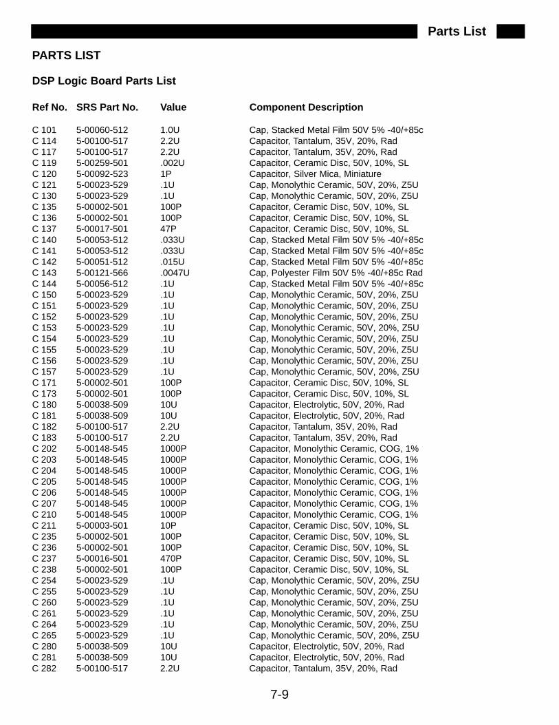
Parts List
7-9
PARTS LIST
DSP Logic Board Parts List
Ref No. SRS Part No. Value Component Description
C 101 5-00060-512 1.0U Cap, Stacked Metal Film 50V 5% -40/+85c C 114 5-00100-517 2.2U Capacitor, Tantalum, 35V, 20%, Rad C 117 5-00100-517 2.2U Capacitor, Tantalum, 35V, 20%, Rad C 119 5-00259-501 .002U Capacitor, Ceramic Disc, 50V, 10%, SLC 120 5-00092-523 1P Capacitor, Silver Mica, Miniature C 121 5-00023-529 .1U Cap, Monolythic Ceramic, 50V, 20%, Z5U C 130 5-00023-529 .1U Cap, Monolythic Ceramic, 50V, 20%, Z5U C 135 5-00002-501 100P Capacitor, Ceramic Disc, 50V, 10%, SLC 136 5-00002-501 100P Capacitor, Ceramic Disc, 50V, 10%, SLC 137 5-00017-501 47P Capacitor, Ceramic Disc, 50V, 10%, SLC 140 5-00053-512 .033U Cap, Stacked Metal Film 50V 5% -40/+85c C 141 5-00053-512 .033U Cap, Stacked Metal Film 50V 5% -40/+85c C 142 5-00051-512 .015U Cap, Stacked Metal Film 50V 5% -40/+85c C 143 5-00121-566 .0047U Cap, Polyester Film 50V 5% -40/+85c Rad C 144 5-00056-512 .1U Cap, Stacked Metal Film 50V 5% -40/+85c C 150 5-00023-529 .1U Cap, Monolythic Ceramic, 50V, 20%, Z5U C 151 5-00023-529 .1U Cap, Monolythic Ceramic, 50V, 20%, Z5U C 152 5-00023-529 .1U Cap, Monolythic Ceramic, 50V, 20%, Z5U C 153 5-00023-529 .1U Cap, Monolythic Ceramic, 50V, 20%, Z5U C 154 5-00023-529 .1U Cap, Monolythic Ceramic, 50V, 20%, Z5U C 155 5-00023-529 .1U Cap, Monolythic Ceramic, 50V, 20%, Z5U C 156 5-00023-529 .1U Cap, Monolythic Ceramic, 50V, 20%, Z5U C 157 5-00023-529 .1U Cap, Monolythic Ceramic, 50V, 20%, Z5U C 171 5-00002-501 100P Capacitor, Ceramic Disc, 50V, 10%, SLC 173 5-00002-501 100P Capacitor, Ceramic Disc, 50V, 10%, SLC 180 5-00038-509 10U Capacitor, Electrolytic, 50V, 20%, Rad C 181 5-00038-509 10U Capacitor, Electrolytic, 50V, 20%, Rad C 182 5-00100-517 2.2U Capacitor, Tantalum, 35V, 20%, Rad C 183 5-00100-517 2.2U Capacitor, Tantalum, 35V, 20%, Rad C 202 5-00148-545 1000P Capacitor, Monolythic Ceramic, COG, 1% C 203 5-00148-545 1000P Capacitor, Monolythic Ceramic, COG, 1% C 204 5-00148-545 1000P Capacitor, Monolythic Ceramic, COG, 1% C 205 5-00148-545 1000P Capacitor, Monolythic Ceramic, COG, 1% C 206 5-00148-545 1000P Capacitor, Monolythic Ceramic, COG, 1% C 207 5-00148-545 1000P Capacitor, Monolythic Ceramic, COG, 1% C 210 5-00148-545 1000P Capacitor, Monolythic Ceramic, COG, 1% C 211 5-00003-501 10P Capacitor, Ceramic Disc, 50V, 10%, SLC 235 5-00002-501 100P Capacitor, Ceramic Disc, 50V, 10%, SLC 236 5-00002-501 100P Capacitor, Ceramic Disc, 50V, 10%, SLC 237 5-00016-501 470P Capacitor, Ceramic Disc, 50V, 10%, SLC 238 5-00002-501 100P Capacitor, Ceramic Disc, 50V, 10%, SLC 254 5-00023-529 .1U Cap, Monolythic Ceramic, 50V, 20%, Z5U C 255 5-00023-529 .1U Cap, Monolythic Ceramic, 50V, 20%, Z5U C 260 5-00023-529 .1U Cap, Monolythic Ceramic, 50V, 20%, Z5U C 261 5-00023-529 .1U Cap, Monolythic Ceramic, 50V, 20%, Z5U C 264 5-00023-529 .1U Cap, Monolythic Ceramic, 50V, 20%, Z5U C 265 5-00023-529 .1U Cap, Monolythic Ceramic, 50V, 20%, Z5U C 280 5-00038-509 10U Capacitor, Electrolytic, 50V, 20%, Rad C 281 5-00038-509 10U Capacitor, Electrolytic, 50V, 20%, Rad C 282 5-00100-517 2.2U Capacitor, Tantalum, 35V, 20%, Rad
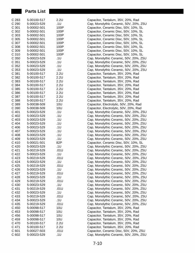
C 283 5-00100-517 2.2U Capacitor, Tantalum, 35V, 20%, Rad C 290 5-00023-529 .1U Cap, Monolythic Ceramic, 50V, 20%, Z5U C 301 5-00002-501 100P Capacitor, Ceramic Disc, 50V, 10%, SLC 302 5-00002-501 100P Capacitor, Ceramic Disc, 50V, 10%, SLC 303 5-00002-501 100P Capacitor, Ceramic Disc, 50V, 10%, SLC 305 5-00002-501 100P Capacitor, Ceramic Disc, 50V, 10%, SLC 307 5-00002-501 100P Capacitor, Ceramic Disc, 50V, 10%, SLC 308 5-00002-501 100P Capacitor, Ceramic Disc, 50V, 10%, SLC 309 5-00002-501 100P Capacitor, Ceramic Disc, 50V, 10%, SLC 310 5-00002-501 100P Capacitor, Ceramic Disc, 50V, 10%, SLC 350 5-00023-529 .1U Cap, Monolythic Ceramic, 50V, 20%, Z5U C 351 5-00023-529 .1U Cap, Monolythic Ceramic, 50V, 20%, Z5U C 352 5-00023-529 .1U Cap, Monolythic Ceramic, 50V, 20%, Z5U C 353 5-00023-529 .1U Cap, Monolythic Ceramic, 50V, 20%, Z5U C 381 5-00100-517 2.2U Capacitor, Tantalum, 35V, 20%, Rad C 382 5-00100-517 2.2U Capacitor, Tantalum, 35V, 20%, Rad C 383 5-00100-517 2.2U Capacitor, Tantalum, 35V, 20%, Rad C 384 5-00100-517 2.2U Capacitor, Tantalum, 35V, 20%, Rad C 385 5-00100-517 2.2U Capacitor, Tantalum, 35V, 20%, Rad C 386 5-00100-517 2.2U Capacitor, Tantalum, 35V, 20%, Rad C 387 5-00100-517 2.2U Capacitor, Tantalum, 35V, 20%, Rad C 388 5-00100-517 2.2U Capacitor, Tantalum, 35V, 20%, Rad C 389 5-00038-509 10U Capacitor, Electrolytic, 50V, 20%, Rad C 390 5-00038-509 10U Capacitor, Electrolytic, 50V, 20%, Rad C 401 5-00023-529 .1U Cap, Monolythic Ceramic, 50V, 20%, Z5U C 402 5-00023-529 .1U Cap, Monolythic Ceramic, 50V, 20%, Z5U C 403 5-00023-529 .1U Cap, Monolythic Ceramic, 50V, 20%, Z5U C 404 5-00023-529 .1U Cap, Monolythic Ceramic, 50V, 20%, Z5U C 406 5-00023-529 .1U Cap, Monolythic Ceramic, 50V, 20%, Z5U C 407 5-00023-529 .1U Cap, Monolythic Ceramic, 50V, 20%, Z5U C 408 5-00023-529 .1U Cap, Monolythic Ceramic, 50V, 20%, Z5U C 409 5-00023-529 .1U Cap, Monolythic Ceramic, 50V, 20%, Z5U C 410 5-00021-501 82P Capacitor, Ceramic Disc, 50V, 10%, SLC 420 5-00023-529 .1U Cap, Monolythic Ceramic, 50V, 20%, Z5U C 421 5-00219-529 .01U Cap, Monolythic Ceramic, 50V, 20%, Z5U C 422 5-00023-529 .1U Cap, Monolythic Ceramic, 50V, 20%, Z5U C 423 5-00219-529 .01U Cap, Monolythic Ceramic, 50V, 20%, Z5U C 424 5-00023-529 .1U Cap, Monolythic Ceramic, 50V, 20%, Z5U C 425 5-00219-529 .01U Cap, Monolythic Ceramic, 50V, 20%, Z5U C 426 5-00023-529 .1U Cap, Monolythic Ceramic, 50V, 20%, Z5U C 427 5-00219-529 .01U Cap, Monolythic Ceramic, 50V, 20%, Z5U C 428 5-00023-529 .1U Cap, Monolythic Ceramic, 50V, 20%, Z5U C 429 5-00219-529 .01U Cap, Monolythic Ceramic, 50V, 20%, Z5U C 430 5-00023-529 .1U Cap, Monolythic Ceramic, 50V, 20%, Z5U C 431 5-00219-529 .01U Cap, Monolythic Ceramic, 50V, 20%, Z5U C 432 5-00023-529 .1U Cap, Monolythic Ceramic, 50V, 20%, Z5U C 433 5-00219-529 .01U Cap, Monolythic Ceramic, 50V, 20%, Z5U C 434 5-00023-529 .1U Cap, Monolythic Ceramic, 50V, 20%, Z5U C 435 5-00219-529 .01U Cap, Monolythic Ceramic, 50V, 20%, Z5U C 450 5-00098-517 10U Capacitor, Tantalum, 35V, 20%, Rad C 453 5-00098-517 10U Capacitor, Tantalum, 35V, 20%, Rad C 456 5-00098-517 10U Capacitor, Tantalum, 35V, 20%, Rad C 459 5-00098-517 10U Capacitor, Tantalum, 35V, 20%, Rad C 470 5-00100-517 2.2U Capacitor, Tantalum, 35V, 20%, Rad C 471 5-00100-517 2.2U Capacitor, Tantalum, 35V, 20%, Rad C 601 5-00027-503 .01U Capacitor, Ceramic Disc, 50V, 20%, Z5U C 602 5-00023-529 .1U Cap, Monolythic Ceramic, 50V, 20%, Z5U
7-10
Parts List
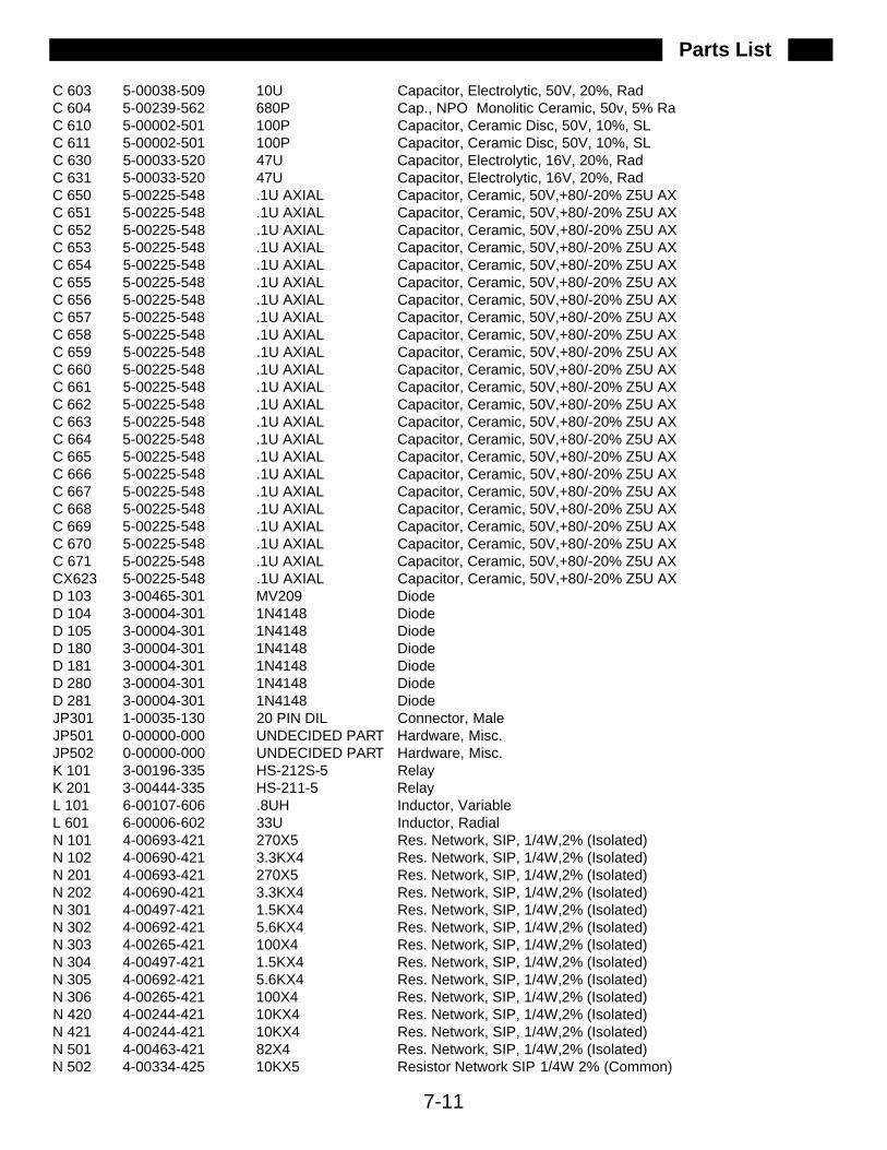
7-11
C 603 5-00038-509 10U Capacitor, Electrolytic, 50V, 20%, Rad C 604 5-00239-562 680P Cap., NPO Monolitic Ceramic, 50v, 5% RaC 610 5-00002-501 100P Capacitor, Ceramic Disc, 50V, 10%, SLC 611 5-00002-501 100P Capacitor, Ceramic Disc, 50V, 10%, SLC 630 5-00033-520 47U Capacitor, Electrolytic, 16V, 20%, Rad C 631 5-00033-520 47U Capacitor, Electrolytic, 16V, 20%, Rad C 650 5-00225-548 .1U AXIAL Capacitor, Ceramic, 50V,+80/-20% Z5U AX C 651 5-00225-548 .1U AXIAL Capacitor, Ceramic, 50V,+80/-20% Z5U AX C 652 5-00225-548 .1U AXIAL Capacitor, Ceramic, 50V,+80/-20% Z5U AX C 653 5-00225-548 .1U AXIAL Capacitor, Ceramic, 50V,+80/-20% Z5U AX C 654 5-00225-548 .1U AXIAL Capacitor, Ceramic, 50V,+80/-20% Z5U AX C 655 5-00225-548 .1U AXIAL Capacitor, Ceramic, 50V,+80/-20% Z5U AX C 656 5-00225-548 .1U AXIAL Capacitor, Ceramic, 50V,+80/-20% Z5U AX C 657 5-00225-548 .1U AXIAL Capacitor, Ceramic, 50V,+80/-20% Z5U AX C 658 5-00225-548 .1U AXIAL Capacitor, Ceramic, 50V,+80/-20% Z5U AX C 659 5-00225-548 .1U AXIAL Capacitor, Ceramic, 50V,+80/-20% Z5U AX C 660 5-00225-548 .1U AXIAL Capacitor, Ceramic, 50V,+80/-20% Z5U AX C 661 5-00225-548 .1U AXIAL Capacitor, Ceramic, 50V,+80/-20% Z5U AX C 662 5-00225-548 .1U AXIAL Capacitor, Ceramic, 50V,+80/-20% Z5U AX C 663 5-00225-548 .1U AXIAL Capacitor, Ceramic, 50V,+80/-20% Z5U AX C 664 5-00225-548 .1U AXIAL Capacitor, Ceramic, 50V,+80/-20% Z5U AX C 665 5-00225-548 .1U AXIAL Capacitor, Ceramic, 50V,+80/-20% Z5U AX C 666 5-00225-548 .1U AXIAL Capacitor, Ceramic, 50V,+80/-20% Z5U AX C 667 5-00225-548 .1U AXIAL Capacitor, Ceramic, 50V,+80/-20% Z5U AX C 668 5-00225-548 .1U AXIAL Capacitor, Ceramic, 50V,+80/-20% Z5U AX C 669 5-00225-548 .1U AXIAL Capacitor, Ceramic, 50V,+80/-20% Z5U AX C 670 5-00225-548 .1U AXIAL Capacitor, Ceramic, 50V,+80/-20% Z5U AX C 671 5-00225-548 .1U AXIAL Capacitor, Ceramic, 50V,+80/-20% Z5U AX CX623 5-00225-548 .1U AXIAL Capacitor, Ceramic, 50V,+80/-20% Z5U AX D 103 3-00465-301 MV209 Diode D 104 3-00004-301 1N4148 Diode D 105 3-00004-301 1N4148 Diode D 180 3-00004-301 1N4148 Diode D 181 3-00004-301 1N4148 Diode D 280 3-00004-301 1N4148 Diode D 281 3-00004-301 1N4148 Diode JP301 1-00035-130 20 PIN DIL Connector, Male JP501 0-00000-000 UNDECIDED PART Hardware, Misc. JP502 0-00000-000 UNDECIDED PART Hardware, Misc. K 101 3-00196-335 HS-212S-5 Relay K 201 3-00444-335 HS-211-5 Relay L 101 6-00107-606 .8UH Inductor, Variable L 601 6-00006-602 33U Inductor, Radial N 101 4-00693-421 270X5 Res. Network, SIP, 1/4W,2% (Isolated) N 102 4-00690-421 3.3KX4 Res. Network, SIP, 1/4W,2% (Isolated) N 201 4-00693-421 270X5 Res. Network, SIP, 1/4W,2% (Isolated) N 202 4-00690-421 3.3KX4 Res. Network, SIP, 1/4W,2% (Isolated) N 301 4-00497-421 1.5KX4 Res. Network, SIP, 1/4W,2% (Isolated) N 302 4-00692-421 5.6KX4 Res. Network, SIP, 1/4W,2% (Isolated) N 303 4-00265-421 100X4 Res. Network, SIP, 1/4W,2% (Isolated) N 304 4-00497-421 1.5KX4 Res. Network, SIP, 1/4W,2% (Isolated) N 305 4-00692-421 5.6KX4 Res. Network, SIP, 1/4W,2% (Isolated) N 306 4-00265-421 100X4 Res. Network, SIP, 1/4W,2% (Isolated) N 420 4-00244-421 10KX4 Res. Network, SIP, 1/4W,2% (Isolated) N 421 4-00244-421 10KX4 Res. Network, SIP, 1/4W,2% (Isolated) N 501 4-00463-421 82X4 Res. Network, SIP, 1/4W,2% (Isolated) N 502 4-00334-425 10KX5 Resistor Network SIP 1/4W 2% (Common)
Parts List
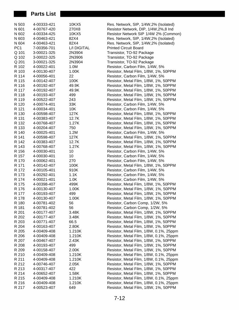
N 503 4-00333-421 10KX5 Res. Network, SIP, 1/4W,2% (Isolated) N 601 4-00767-420 270X8 Resistor Network, DIP, 1/4W,2%,8 Ind N 602 4-00334-425 10KX5 Resistor Network SIP 1/4W 2% (Common) N 603 4-00463-421 82X4 Res. Network, SIP, 1/4W,2% (Isolated) N 604 4-00463-421 82X4 Res. Network, SIP, 1/4W,2% (Isolated) PC1 7-00356-701 L/I DIGITAL Printed Circuit Board Q 101 3-00021-325 2N3904 Transistor, TO-92 Package Q 102 3-00022-325 2N3906 Transistor, TO-92 Package Q 201 3-00021-325 2N3904 Transistor, TO-92 Package R 102 4-00022-401 1.0M Resistor, Carbon Film, 1/4W, 5% R 103 4-00130-407 1.00K Resistor, Metal Film, 1/8W, 1%, 50PPM R 114 4-00056-401 22 Resistor, Carbon Film, 1/4W, 5% R 115 4-00142-407 100K Resistor, Metal Film, 1/8W, 1%, 50PPM R 116 4-00192-407 49.9K Resistor, Metal Film, 1/8W, 1%, 50PPM R 117 4-00192-407 49.9K Resistor, Metal Film, 1/8W, 1%, 50PPM R 118 4-00193-407 499 Resistor, Metal Film, 1/8W, 1%, 50PPM R 119 4-00522-407 243 Resistor, Metal Film, 1/8W, 1%, 50PPM R 120 4-00074-401 33K Resistor, Carbon Film, 1/4W, 5% R 121 4-00034-401 10K Resistor, Carbon Film, 1/4W, 5% R 130 4-00598-407 127K Resistor, Metal Film, 1/8W, 1%, 50PPM R 131 4-00383-407 12.7K Resistor, Metal Film, 1/8W, 1%, 50PPM R 132 4-00768-407 1.27K Resistor, Metal Film, 1/8W, 1%, 50PPM R 133 4-00204-407 750 Resistor, Metal Film, 1/8W, 1%, 50PPM R 140 4-00025-401 1.2M Resistor, Carbon Film, 1/4W, 5% R 141 4-00598-407 127K Resistor, Metal Film, 1/8W, 1%, 50PPM R 142 4-00383-407 12.7K Resistor, Metal Film, 1/8W, 1%, 50PPM R 143 4-00768-407 1.27K Resistor, Metal Film, 1/8W, 1%, 50PPM R 156 4-00030-401 10 Resistor, Carbon Film, 1/4W, 5% R 157 4-00030-401 10 Resistor, Carbon Film, 1/4W, 5% R 170 4-00062-401 270 Resistor, Carbon Film, 1/4W, 5% R 171 4-00142-407 100K Resistor, Metal Film, 1/8W, 1%, 50PPM R 172 4-00105-401 910K Resistor, Carbon Film, 1/4W, 5% R 173 4-00292-401 1.1K Resistor, Carbon Film, 1/4W, 5% R 174 4-00021-401 1.0K Resistor, Carbon Film, 1/4W, 5% R 175 4-00398-407 499K Resistor, Metal Film, 1/8W, 1%, 50PPM R 176 4-00130-407 1.00K Resistor, Metal Film, 1/8W, 1%, 50PPM R 177 4-00193-407 499 Resistor, Metal Film, 1/8W, 1%, 50PPM R 178 4-00130-407 1.00K Resistor, Metal Film, 1/8W, 1%, 50PPM R 180 4-00781-402 56 Resistor, Carbon Comp, 1/2W, 5% R 181 4-00781-402 56 Resistor, Carbon Comp, 1/2W, 5% R 201 4-00177-407 3.48K Resistor, Metal Film, 1/8W, 1%, 50PPM R 202 4-00177-407 3.48K Resistor, Metal Film, 1/8W, 1%, 50PPM R 203 4-00771-407 66.5 Resistor, Metal Film, 1/8W, 1%, 50PPM R 204 4-00163-407 2.80K Resistor, Metal Film, 1/8W, 1%, 50PPM R 205 4-00409-408 1.210K Resistor, Metal Film, 1/8W, 0.1%, 25ppm R 206 4-00409-408 1.210K Resistor, Metal Film, 1/8W, 0.1%, 25ppm R 207 4-00467-407 2.43K Resistor, Metal Film, 1/8W, 1%, 50PPM R 208 4-00193-407 499 Resistor, Metal Film, 1/8W, 1%, 50PPM R 209 4-00158-407 2.00K Resistor, Metal Film, 1/8W, 1%, 50PPM R 210 4-00409-408 1.210K Resistor, Metal Film, 1/8W, 0.1%, 25ppm R 211 4-00409-408 1.210K Resistor, Metal Film, 1/8W, 0.1%, 25ppm R 212 4-00746-407 2.05K Resistor, Metal Film, 1/8W, 1%, 50PPM R 213 4-00317-407 422 Resistor, Metal Film, 1/8W, 1%, 50PPM R 214 4-00652-407 1.58K Resistor, Metal Film, 1/8W, 1%, 50PPM R 215 4-00409-408 1.210K Resistor, Metal Film, 1/8W, 0.1%, 25ppm R 216 4-00409-408 1.210K Resistor, Metal Film, 1/8W, 0.1%, 25ppm R 217 4-00523-407 649 Resistor, Metal Film, 1/8W, 1%, 50PPM
7-12
Parts List
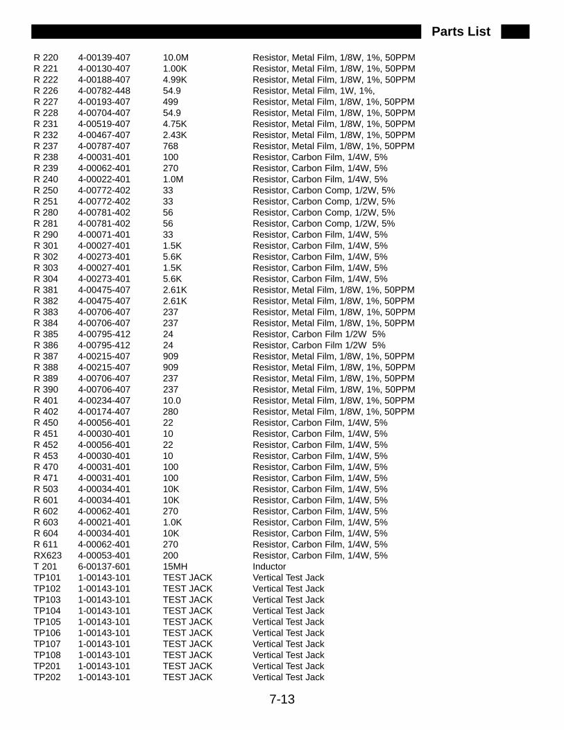
7-13
R 220 4-00139-407 10.0M Resistor, Metal Film, 1/8W, 1%, 50PPM R 221 4-00130-407 1.00K Resistor, Metal Film, 1/8W, 1%, 50PPM R 222 4-00188-407 4.99K Resistor, Metal Film, 1/8W, 1%, 50PPM R 226 4-00782-448 54.9 Resistor, Metal Film, 1W, 1%, R 227 4-00193-407 499 Resistor, Metal Film, 1/8W, 1%, 50PPM R 228 4-00704-407 54.9 Resistor, Metal Film, 1/8W, 1%, 50PPM R 231 4-00519-407 4.75K Resistor, Metal Film, 1/8W, 1%, 50PPM R 232 4-00467-407 2.43K Resistor, Metal Film, 1/8W, 1%, 50PPM R 237 4-00787-407 768 Resistor, Metal Film, 1/8W, 1%, 50PPM R 238 4-00031-401 100 Resistor, Carbon Film, 1/4W, 5% R 239 4-00062-401 270 Resistor, Carbon Film, 1/4W, 5% R 240 4-00022-401 1.0M Resistor, Carbon Film, 1/4W, 5% R 250 4-00772-402 33 Resistor, Carbon Comp, 1/2W, 5% R 251 4-00772-402 33 Resistor, Carbon Comp, 1/2W, 5% R 280 4-00781-402 56 Resistor, Carbon Comp, 1/2W, 5% R 281 4-00781-402 56 Resistor, Carbon Comp, 1/2W, 5% R 290 4-00071-401 33 Resistor, Carbon Film, 1/4W, 5% R 301 4-00027-401 1.5K Resistor, Carbon Film, 1/4W, 5% R 302 4-00273-401 5.6K Resistor, Carbon Film, 1/4W, 5% R 303 4-00027-401 1.5K Resistor, Carbon Film, 1/4W, 5% R 304 4-00273-401 5.6K Resistor, Carbon Film, 1/4W, 5% R 381 4-00475-407 2.61K Resistor, Metal Film, 1/8W, 1%, 50PPM R 382 4-00475-407 2.61K Resistor, Metal Film, 1/8W, 1%, 50PPM R 383 4-00706-407 237 Resistor, Metal Film, 1/8W, 1%, 50PPM R 384 4-00706-407 237 Resistor, Metal Film, 1/8W, 1%, 50PPM R 385 4-00795-412 24 Resistor, Carbon Film 1/2W 5% R 386 4-00795-412 24 Resistor, Carbon Film 1/2W 5% R 387 4-00215-407 909 Resistor, Metal Film, 1/8W, 1%, 50PPM R 388 4-00215-407 909 Resistor, Metal Film, 1/8W, 1%, 50PPM R 389 4-00706-407 237 Resistor, Metal Film, 1/8W, 1%, 50PPM R 390 4-00706-407 237 Resistor, Metal Film, 1/8W, 1%, 50PPM R 401 4-00234-407 10.0 Resistor, Metal Film, 1/8W, 1%, 50PPM R 402 4-00174-407 280 Resistor, Metal Film, 1/8W, 1%, 50PPM R 450 4-00056-401 22 Resistor, Carbon Film, 1/4W, 5% R 451 4-00030-401 10 Resistor, Carbon Film, 1/4W, 5% R 452 4-00056-401 22 Resistor, Carbon Film, 1/4W, 5% R 453 4-00030-401 10 Resistor, Carbon Film, 1/4W, 5% R 470 4-00031-401 100 Resistor, Carbon Film, 1/4W, 5% R 471 4-00031-401 100 Resistor, Carbon Film, 1/4W, 5% R 503 4-00034-401 10K Resistor, Carbon Film, 1/4W, 5% R 601 4-00034-401 10K Resistor, Carbon Film, 1/4W, 5% R 602 4-00062-401 270 Resistor, Carbon Film, 1/4W, 5% R 603 4-00021-401 1.0K Resistor, Carbon Film, 1/4W, 5% R 604 4-00034-401 10K Resistor, Carbon Film, 1/4W, 5% R 611 4-00062-401 270 Resistor, Carbon Film, 1/4W, 5% RX623 4-00053-401 200 Resistor, Carbon Film, 1/4W, 5% T 201 6-00137-601 15MH Inductor TP101 1-00143-101 TEST JACK Vertical Test Jack TP102 1-00143-101 TEST JACK Vertical Test Jack TP103 1-00143-101 TEST JACK Vertical Test Jack TP104 1-00143-101 TEST JACK Vertical Test Jack TP105 1-00143-101 TEST JACK Vertical Test Jack TP106 1-00143-101 TEST JACK Vertical Test Jack TP107 1-00143-101 TEST JACK Vertical Test Jack TP108 1-00143-101 TEST JACK Vertical Test Jack TP201 1-00143-101 TEST JACK Vertical Test Jack TP202 1-00143-101 TEST JACK Vertical Test Jack
Parts List
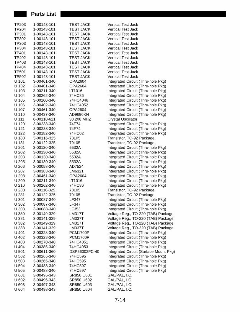
TP203 1-00143-101 TEST JACK Vertical Test Jack TP204 1-00143-101 TEST JACK Vertical Test Jack TP301 1-00143-101 TEST JACK Vertical Test Jack TP302 1-00143-101 TEST JACK Vertical Test Jack TP303 1-00143-101 TEST JACK Vertical Test Jack TP304 1-00143-101 TEST JACK Vertical Test Jack TP401 1-00143-101 TEST JACK Vertical Test Jack TP402 1-00143-101 TEST JACK Vertical Test Jack TP403 1-00143-101 TEST JACK Vertical Test Jack TP404 1-00143-101 TEST JACK Vertical Test Jack TP501 1-00143-101 TEST JACK Vertical Test Jack TP502 1-00143-101 TEST JACK Vertical Test Jack U 101 3-00461-340 OPA2604 Integrated Circuit (Thru-hole Pkg) U 102 3-00461-340 OPA2604 Integrated Circuit (Thru-hole Pkg) U 103 3-00211-340 LT1016 Integrated Circuit (Thru-hole Pkg) U 104 3-00262-340 74HC86 Integrated Circuit (Thru-hole Pkg) U 105 3-00160-340 74HC4046 Integrated Circuit (Thru-hole Pkg) U 106 3-00402-340 74HC4052 Integrated Circuit (Thru-hole Pkg) U 107 3-00461-340 OPA2604 Integrated Circuit (Thru-hole Pkg) U 110 3-00437-340 AD9696KN Integrated Circuit (Thru-hole Pkg) U 111 6-00110-621 30.208 MHZ Crystal Oscillator U 120 3-00238-340 74F74 Integrated Circuit (Thru-hole Pkg) U 121 3-00238-340 74F74 Integrated Circuit (Thru-hole Pkg) U 122 3-00182-340 74HC02 Integrated Circuit (Thru-hole Pkg) U 180 3-00116-325 78L05 Transistor, TO-92 Package U 181 3-00122-325 79L05 Transistor, TO-92 Package U 201 3-00130-340 5532A Integrated Circuit (Thru-hole Pkg) U 202 3-00130-340 5532A Integrated Circuit (Thru-hole Pkg) U 203 3-00130-340 5532A Integrated Circuit (Thru-hole Pkg) U 205 3-00130-340 5532A Integrated Circuit (Thru-hole Pkg) U 206 3-00058-340 AD7524 Integrated Circuit (Thru-hole Pkg) U 207 3-00383-340 LM6321 Integrated Circuit (Thru-hole Pkg) U 208 3-00461-340 OPA2604 Integrated Circuit (Thru-hole Pkg) U 209 3-00211-340 LT1016 Integrated Circuit (Thru-hole Pkg) U 210 3-00262-340 74HC86 Integrated Circuit (Thru-hole Pkg) U 280 3-00116-325 78L05 Transistor, TO-92 Package U 281 3-00122-325 79L05 Transistor, TO-92 Package U 301 3-00087-340 LF347 Integrated Circuit (Thru-hole Pkg) U 302 3-00087-340 LF347 Integrated Circuit (Thru-hole Pkg) U 303 3-00088-340 LF353 Integrated Circuit (Thru-hole Pkg) U 380 3-00149-329 LM317T Voltage Reg., TO-220 (TAB) Package U 381 3-00141-329 LM337T Voltage Reg., TO-220 (TAB) Package U 382 3-00149-329 LM317T Voltage Reg., TO-220 (TAB) Package U 383 3-00141-329 LM337T Voltage Reg., TO-220 (TAB) Package U 401 3-00328-340 PCM1700P Integrated Circuit (Thru-hole Pkg) U 402 3-00328-340 PCM1700P Integrated Circuit (Thru-hole Pkg) U 403 3-00270-340 74HC4051 Integrated Circuit (Thru-hole Pkg) U 404 3-00385-340 74HC4053 Integrated Circuit (Thru-hole Pkg) U 501 3-00611-360 DSP56002FC-40 Integrated Circuit (Surface Mount Pkg) U 502 3-00265-340 74HC595 Integrated Circuit (Thru-hole Pkg) U 503 3-00265-340 74HC595 Integrated Circuit (Thru-hole Pkg) U 504 3-00488-340 74HC597 Integrated Circuit (Thru-hole Pkg) U 505 3-00488-340 74HC597 Integrated Circuit (Thru-hole Pkg) U 601 3-00495-343 SR850 U601 GAL/PAL, I.C. U 602 3-00496-343 SR850 U602 GAL/PAL, I.C. U 603 3-00497-343 SR850 U603 GAL/PAL, I.C. U 604 3-00498-343 SR850 U604 GAL/PAL, I.C.
7-14
Parts List
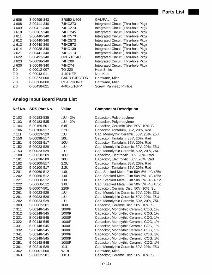
7-15
U 606 3-00499-343 SR850 U606 GAL/PAL, I.C. U 608 3-00411-340 74HC273 Integrated Circuit (Thru-hole Pkg) U 609 3-00411-340 74HC273 Integrated Circuit (Thru-hole Pkg) U 610 3-00387-340 74HC245 Integrated Circuit (Thru-hole Pkg) U 611 3-00440-340 74HC573 Integrated Circuit (Thru-hole Pkg) U 612 3-00440-340 74HC573 Integrated Circuit (Thru-hole Pkg) U 613 3-00440-340 74HC573 Integrated Circuit (Thru-hole Pkg) U 614 3-00038-340 74HC139 Integrated Circuit (Thru-hole Pkg) U 621 3-00441-340 74HC113 Integrated Circuit (Thru-hole Pkg) U 622 3-00491-340 UPD71054C Integrated Circuit (Thru-hole Pkg) U 623 3-00036-340 74HC00 Integrated Circuit (Thru-hole Pkg) U 630 3-00049-340 74HC74 Integrated Circuit (Thru-hole Pkg) Z 0 0-00012-007 TO-220 Heat Sinks Z 0 0-00043-011 4-40 KEP Nut, Kep Z 0 0-00373-000 CARD EJECTOR Hardware, Misc. Z 0 0-00388-000 RCA PHONO Hardware, Misc. Z 0 0-00438-021 4-40X5/16PP Screw, Panhead Phillips
Analog Input Board Parts List
Ref No. SRS Part No. Value Component Description
C 102 5-00183-535 .1U - 2% Capacitor, Polypropylene C 103 5-00183-535 .1U - 2% Capacitor, Polypropylene C 104 5-00159-501 6.8P Capacitor, Ceramic Disc, 50V, 10%, SLC 106 5-00100-517 2.2U Capacitor, Tantalum, 35V, 20%, Rad C 111 5-00023-529 .1U Cap, Monolythic Ceramic, 50V, 20%, Z5U C 150 5-00098-517 10U Capacitor, Tantalum, 35V, 20%, Rad C 151 5-00098-517 10U Capacitor, Tantalum, 35V, 20%, Rad C 152 5-00023-529 .1U Cap, Monolythic Ceramic, 50V, 20%, Z5U C 153 5-00023-529 .1U Cap, Monolythic Ceramic, 50V, 20%, Z5U C 180 5-00038-509 10U Capacitor, Electrolytic, 50V, 20%, Rad C 181 5-00038-509 10U Capacitor, Electrolytic, 50V, 20%, Rad C 182 5-00100-517 2.2U Capacitor, Tantalum, 35V, 20%, Rad C 183 5-00100-517 2.2U Capacitor, Tantalum, 35V, 20%, Rad C 201 5-00060-512 1.0U Cap, Stacked Metal Film 50V 5% -40/+85c C 202 5-00060-512 1.0U Cap, Stacked Metal Film 50V 5% -40/+85c C 221 5-00060-512 1.0U Cap, Stacked Metal Film 50V 5% -40/+85c C 222 5-00060-512 1.0U Cap, Stacked Metal Film 50V 5% -40/+85c C 225 5-00007-501 220P Capacitor, Ceramic Disc, 50V, 10%, SLC 261 5-00023-529 .1U Cap, Monolythic Ceramic, 50V, 20%, Z5U C 281 5-00023-529 .1U Cap, Monolythic Ceramic, 50V, 20%, Z5U C 282 5-00023-529 .1U Cap, Monolythic Ceramic, 50V, 20%, Z5U C 303 5-00002-501 100P Capacitor, Ceramic Disc, 50V, 10%, SLC 311 5-00148-545 1000P Capacitor, Monolythic Ceramic, COG, 1% C 312 5-00148-545 1000P Capacitor, Monolythic Ceramic, COG, 1% C 321 5-00148-545 1000P Capacitor, Monolythic Ceramic, COG, 1% C 322 5-00148-545 1000P Capacitor, Monolythic Ceramic, COG, 1% C 331 5-00148-545 1000P Capacitor, Monolythic Ceramic, COG, 1% C 332 5-00148-545 1000P Capacitor, Monolythic Ceramic, COG, 1% C 341 5-00148-545 1000P Capacitor, Monolythic Ceramic, COG, 1% C 342 5-00148-545 1000P Capacitor, Monolythic Ceramic, COG, 1% C 351 5-00148-545 1000P Capacitor, Monolythic Ceramic, COG, 1% C 361 5-00219-529 .01U Cap, Monolythic Ceramic, 50V, 20%, Z5U C 362 0-00001-000 WIRE Hardware, Misc. C 363 5-00022-501 .001U Capacitor, Ceramic Disc, 50V, 10%, SL
Parts List
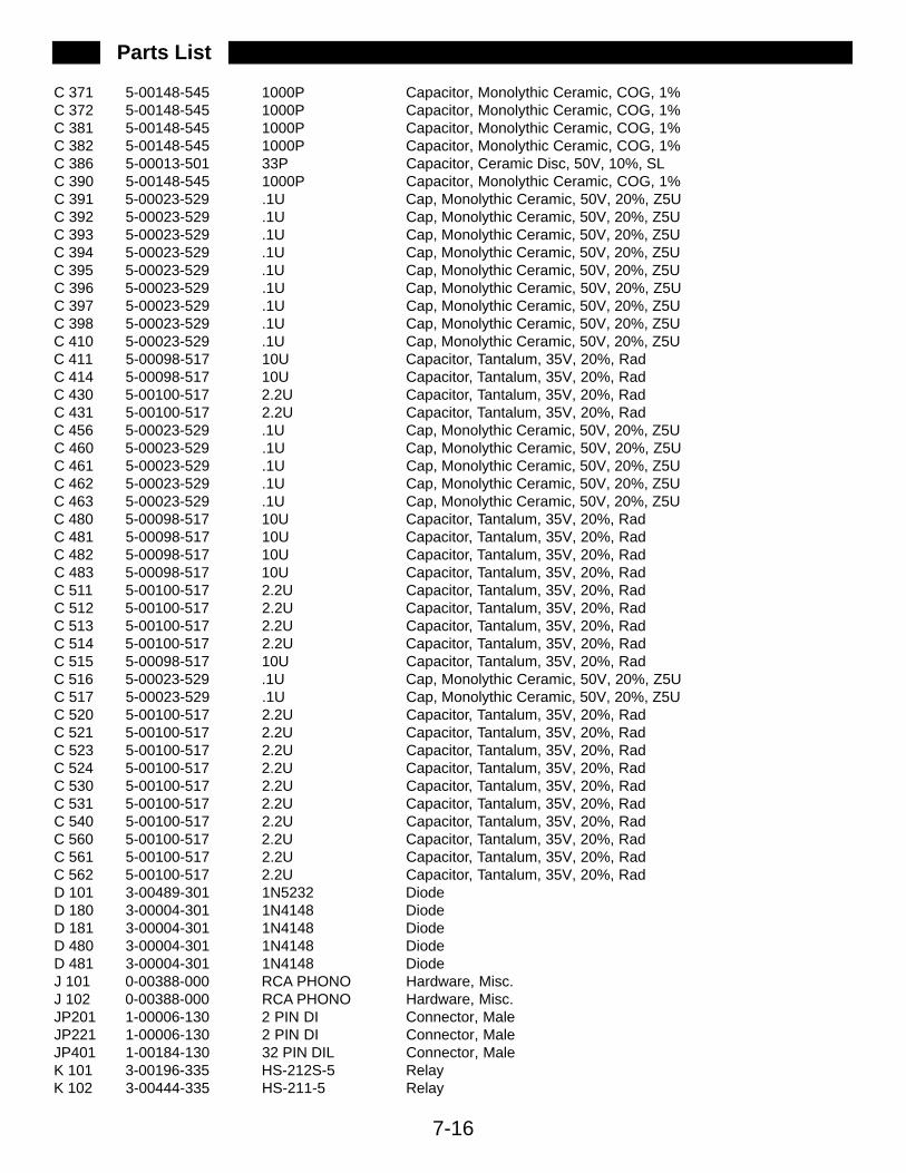
C 371 5-00148-545 1000P Capacitor, Monolythic Ceramic, COG, 1% C 372 5-00148-545 1000P Capacitor, Monolythic Ceramic, COG, 1% C 381 5-00148-545 1000P Capacitor, Monolythic Ceramic, COG, 1% C 382 5-00148-545 1000P Capacitor, Monolythic Ceramic, COG, 1% C 386 5-00013-501 33P Capacitor, Ceramic Disc, 50V, 10%, SLC 390 5-00148-545 1000P Capacitor, Monolythic Ceramic, COG, 1% C 391 5-00023-529 .1U Cap, Monolythic Ceramic, 50V, 20%, Z5U C 392 5-00023-529 .1U Cap, Monolythic Ceramic, 50V, 20%, Z5U C 393 5-00023-529 .1U Cap, Monolythic Ceramic, 50V, 20%, Z5U C 394 5-00023-529 .1U Cap, Monolythic Ceramic, 50V, 20%, Z5U C 395 5-00023-529 .1U Cap, Monolythic Ceramic, 50V, 20%, Z5U C 396 5-00023-529 .1U Cap, Monolythic Ceramic, 50V, 20%, Z5U C 397 5-00023-529 .1U Cap, Monolythic Ceramic, 50V, 20%, Z5U C 398 5-00023-529 .1U Cap, Monolythic Ceramic, 50V, 20%, Z5U C 410 5-00023-529 .1U Cap, Monolythic Ceramic, 50V, 20%, Z5U C 411 5-00098-517 10U Capacitor, Tantalum, 35V, 20%, Rad C 414 5-00098-517 10U Capacitor, Tantalum, 35V, 20%, Rad C 430 5-00100-517 2.2U Capacitor, Tantalum, 35V, 20%, Rad C 431 5-00100-517 2.2U Capacitor, Tantalum, 35V, 20%, Rad C 456 5-00023-529 .1U Cap, Monolythic Ceramic, 50V, 20%, Z5U C 460 5-00023-529 .1U Cap, Monolythic Ceramic, 50V, 20%, Z5U C 461 5-00023-529 .1U Cap, Monolythic Ceramic, 50V, 20%, Z5U C 462 5-00023-529 .1U Cap, Monolythic Ceramic, 50V, 20%, Z5U C 463 5-00023-529 .1U Cap, Monolythic Ceramic, 50V, 20%, Z5U C 480 5-00098-517 10U Capacitor, Tantalum, 35V, 20%, Rad C 481 5-00098-517 10U Capacitor, Tantalum, 35V, 20%, Rad C 482 5-00098-517 10U Capacitor, Tantalum, 35V, 20%, Rad C 483 5-00098-517 10U Capacitor, Tantalum, 35V, 20%, Rad C 511 5-00100-517 2.2U Capacitor, Tantalum, 35V, 20%, Rad C 512 5-00100-517 2.2U Capacitor, Tantalum, 35V, 20%, Rad C 513 5-00100-517 2.2U Capacitor, Tantalum, 35V, 20%, Rad C 514 5-00100-517 2.2U Capacitor, Tantalum, 35V, 20%, Rad C 515 5-00098-517 10U Capacitor, Tantalum, 35V, 20%, Rad C 516 5-00023-529 .1U Cap, Monolythic Ceramic, 50V, 20%, Z5U C 517 5-00023-529 .1U Cap, Monolythic Ceramic, 50V, 20%, Z5U C 520 5-00100-517 2.2U Capacitor, Tantalum, 35V, 20%, Rad C 521 5-00100-517 2.2U Capacitor, Tantalum, 35V, 20%, Rad C 523 5-00100-517 2.2U Capacitor, Tantalum, 35V, 20%, Rad C 524 5-00100-517 2.2U Capacitor, Tantalum, 35V, 20%, Rad C 530 5-00100-517 2.2U Capacitor, Tantalum, 35V, 20%, Rad C 531 5-00100-517 2.2U Capacitor, Tantalum, 35V, 20%, Rad C 540 5-00100-517 2.2U Capacitor, Tantalum, 35V, 20%, Rad C 560 5-00100-517 2.2U Capacitor, Tantalum, 35V, 20%, Rad C 561 5-00100-517 2.2U Capacitor, Tantalum, 35V, 20%, Rad C 562 5-00100-517 2.2U Capacitor, Tantalum, 35V, 20%, Rad D 101 3-00489-301 1N5232 Diode D 180 3-00004-301 1N4148 Diode D 181 3-00004-301 1N4148 Diode D 480 3-00004-301 1N4148 Diode D 481 3-00004-301 1N4148 Diode J 101 0-00388-000 RCA PHONO Hardware, Misc. J 102 0-00388-000 RCA PHONO Hardware, Misc. JP201 1-00006-130 2 PIN DI Connector, Male JP221 1-00006-130 2 PIN DI Connector, Male JP401 1-00184-130 32 PIN DIL Connector, Male K 101 3-00196-335 HS-212S-5 Relay K 102 3-00444-335 HS-211-5 Relay
7-16
Parts List
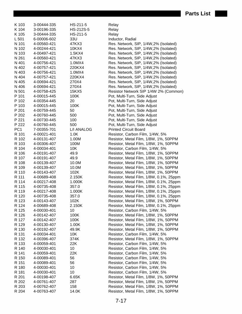
7-17
K 103 3-00444-335 HS-211-5 Relay K 104 3-00196-335 HS-212S-5 Relay K 105 3-00444-335 HS-211-5 Relay L 501 6-00006-602 33U Inductor, Radial N 101 4-00560-421 47KX3 Res. Network, SIP, 1/4W,2% (Isolated) N 102 4-00244-421 10KX4 Res. Network, SIP, 1/4W,2% (Isolated) N 103 4-00497-421 1.5KX4 Res. Network, SIP, 1/4W,2% (Isolated) N 261 4-00560-421 47KX3 Res. Network, SIP, 1/4W,2% (Isolated) N 401 4-00756-421 1.0MX4 Res. Network, SIP, 1/4W,2% (Isolated) N 402 4-00757-421 220KX4 Res. Network, SIP, 1/4W,2% (Isolated) N 403 4-00756-421 1.0MX4 Res. Network, SIP, 1/4W,2% (Isolated) N 404 4-00757-421 220KX4 Res. Network, SIP, 1/4W,2% (Isolated) N 405 4-00694-421 270X4 Res. Network, SIP, 1/4W,2% (Isolated) N 406 4-00694-421 270X4 Res. Network, SIP, 1/4W,2% (Isolated) N 501 4-00758-425 15KX5 Resistor Network SIP 1/4W 2% (Common) P 101 4-00015-445 100K Pot, Multi-Turn, Side Adjust P 102 4-00354-445 20 Pot, Multi-Turn, Side Adjust P 103 4-00015-445 100K Pot, Multi-Turn, Side Adjust P 201 4-00759-445 50 Pot, Multi-Turn, Side Adjust P 202 4-00760-445 500 Pot, Multi-Turn, Side Adjust P 221 4-00730-445 100 Pot, Multi-Turn, Side Adjust P 222 4-00760-445 500 Pot, Multi-Turn, Side Adjust PC1 7-00355-701 L/I ANALOG Printed Circuit Board R 101 4-00021-401 1.0K Resistor, Carbon Film, 1/4W, 5% R 102 4-00131-407 1.00M Resistor, Metal Film, 1/8W, 1%, 50PPM R 103 4-00306-407 100M Resistor, Metal Film, 1/8W, 1%, 50PPM R 104 4-00034-401 10K Resistor, Carbon Film, 1/4W, 5% R 106 4-00191-407 49.9 Resistor, Metal Film, 1/8W, 1%, 50PPM R 107 4-00191-407 49.9 Resistor, Metal Film, 1/8W, 1%, 50PPM R 108 4-00139-407 10.0M Resistor, Metal Film, 1/8W, 1%, 50PPM R 109 4-00139-407 10.0M Resistor, Metal Film, 1/8W, 1%, 50PPM R 110 4-00143-407 102K Resistor, Metal Film, 1/8W, 1%, 50PPM R 111 4-00689-408 2.150K Resistor, Metal Film, 1/8W, 0.1%, 25ppm R 114 4-00217-408 1.000K Resistor, Metal Film, 1/8W, 0.1%, 25ppm R 115 4-00735-408 357.0 Resistor, Metal Film, 1/8W, 0.1%, 25ppm R 119 4-00217-408 1.000K Resistor, Metal Film, 1/8W, 0.1%, 25ppm R 120 4-00735-408 357.0 Resistor, Metal Film, 1/8W, 0.1%, 25ppm R 123 4-00143-407 102K Resistor, Metal Film, 1/8W, 1%, 50PPM R 124 4-00689-408 2.150K Resistor, Metal Film, 1/8W, 0.1%, 25ppm R 125 4-00030-401 10 Resistor, Carbon Film, 1/4W, 5% R 126 4-00142-407 100K Resistor, Metal Film, 1/8W, 1%, 50PPM R 127 4-00142-407 100K Resistor, Metal Film, 1/8W, 1%, 50PPM R 129 4-00130-407 1.00K Resistor, Metal Film, 1/8W, 1%, 50PPM R 130 4-00192-407 49.9K Resistor, Metal Film, 1/8W, 1%, 50PPM R 131 4-00034-401 10K Resistor, Carbon Film, 1/4W, 5% R 132 4-00396-407 374K Resistor, Metal Film, 1/8W, 1%, 50PPM R 133 4-00059-401 22K Resistor, Carbon Film, 1/4W, 5% R 140 4-00030-401 10 Resistor, Carbon Film, 1/4W, 5% R 141 4-00059-401 22K Resistor, Carbon Film, 1/4W, 5% R 150 4-00089-401 56 Resistor, Carbon Film, 1/4W, 5% R 151 4-00089-401 56 Resistor, Carbon Film, 1/4W, 5% R 180 4-00030-401 10 Resistor, Carbon Film, 1/4W, 5% R 181 4-00030-401 10 Resistor, Carbon Film, 1/4W, 5% R 201 4-00198-407 6.65K Resistor, Metal Film, 1/8W, 1%, 50PPM R 202 4-00761-407 287 Resistor, Metal Film, 1/8W, 1%, 50PPM R 203 4-00762-407 158 Resistor, Metal Film, 1/8W, 1%, 50PPM R 204 4-00763-407 14.0K Resistor, Metal Film, 1/8W, 1%, 50PPM
Parts List
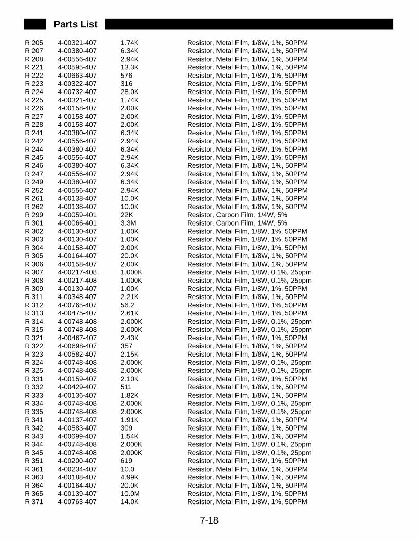
R 205 4-00321-407 1.74K Resistor, Metal Film, 1/8W, 1%, 50PPM R 207 4-00380-407 6.34K Resistor, Metal Film, 1/8W, 1%, 50PPM R 208 4-00556-407 2.94K Resistor, Metal Film, 1/8W, 1%, 50PPM R 221 4-00595-407 13.3K Resistor, Metal Film, 1/8W, 1%, 50PPM R 222 4-00663-407 576 Resistor, Metal Film, 1/8W, 1%, 50PPM R 223 4-00322-407 316 Resistor, Metal Film, 1/8W, 1%, 50PPM R 224 4-00732-407 28.0K Resistor, Metal Film, 1/8W, 1%, 50PPM R 225 4-00321-407 1.74K Resistor, Metal Film, 1/8W, 1%, 50PPM R 226 4-00158-407 2.00K Resistor, Metal Film, 1/8W, 1%, 50PPM R 227 4-00158-407 2.00K Resistor, Metal Film, 1/8W, 1%, 50PPM R 228 4-00158-407 2.00K Resistor, Metal Film, 1/8W, 1%, 50PPM R 241 4-00380-407 6.34K Resistor, Metal Film, 1/8W, 1%, 50PPM R 242 4-00556-407 2.94K Resistor, Metal Film, 1/8W, 1%, 50PPM R 244 4-00380-407 6.34K Resistor, Metal Film, 1/8W, 1%, 50PPM R 245 4-00556-407 2.94K Resistor, Metal Film, 1/8W, 1%, 50PPM R 246 4-00380-407 6.34K Resistor, Metal Film, 1/8W, 1%, 50PPM R 247 4-00556-407 2.94K Resistor, Metal Film, 1/8W, 1%, 50PPM R 249 4-00380-407 6.34K Resistor, Metal Film, 1/8W, 1%, 50PPM R 252 4-00556-407 2.94K Resistor, Metal Film, 1/8W, 1%, 50PPM R 261 4-00138-407 10.0K Resistor, Metal Film, 1/8W, 1%, 50PPM R 262 4-00138-407 10.0K Resistor, Metal Film, 1/8W, 1%, 50PPM R 299 4-00059-401 22K Resistor, Carbon Film, 1/4W, 5% R 301 4-00066-401 3.3M Resistor, Carbon Film, 1/4W, 5% R 302 4-00130-407 1.00K Resistor, Metal Film, 1/8W, 1%, 50PPM R 303 4-00130-407 1.00K Resistor, Metal Film, 1/8W, 1%, 50PPM R 304 4-00158-407 2.00K Resistor, Metal Film, 1/8W, 1%, 50PPM R 305 4-00164-407 20.0K Resistor, Metal Film, 1/8W, 1%, 50PPM R 306 4-00158-407 2.00K Resistor, Metal Film, 1/8W, 1%, 50PPM R 307 4-00217-408 1.000K Resistor, Metal Film, 1/8W, 0.1%, 25ppm R 308 4-00217-408 1.000K Resistor, Metal Film, 1/8W, 0.1%, 25ppm R 309 4-00130-407 1.00K Resistor, Metal Film, 1/8W, 1%, 50PPM R 311 4-00348-407 2.21K Resistor, Metal Film, 1/8W, 1%, 50PPM R 312 4-00765-407 56.2 Resistor, Metal Film, 1/8W, 1%, 50PPM R 313 4-00475-407 2.61K Resistor, Metal Film, 1/8W, 1%, 50PPM R 314 4-00748-408 2.000K Resistor, Metal Film, 1/8W, 0.1%, 25ppm R 315 4-00748-408 2.000K Resistor, Metal Film, 1/8W, 0.1%, 25ppm R 321 4-00467-407 2.43K Resistor, Metal Film, 1/8W, 1%, 50PPM R 322 4-00698-407 357 Resistor, Metal Film, 1/8W, 1%, 50PPM R 323 4-00582-407 2.15K Resistor, Metal Film, 1/8W, 1%, 50PPM R 324 4-00748-408 2.000K Resistor, Metal Film, 1/8W, 0.1%, 25ppm R 325 4-00748-408 2.000K Resistor, Metal Film, 1/8W, 0.1%, 25ppm R 331 4-00159-407 2.10K Resistor, Metal Film, 1/8W, 1%, 50PPM R 332 4-00429-407 511 Resistor, Metal Film, 1/8W, 1%, 50PPM R 333 4-00136-407 1.82K Resistor, Metal Film, 1/8W, 1%, 50PPM R 334 4-00748-408 2.000K Resistor, Metal Film, 1/8W, 0.1%, 25ppm R 335 4-00748-408 2.000K Resistor, Metal Film, 1/8W, 0.1%, 25ppm R 341 4-00137-407 1.91K Resistor, Metal Film, 1/8W, 1%, 50PPM R 342 4-00583-407 309 Resistor, Metal Film, 1/8W, 1%, 50PPM R 343 4-00699-407 1.54K Resistor, Metal Film, 1/8W, 1%, 50PPM R 344 4-00748-408 2.000K Resistor, Metal Film, 1/8W, 0.1%, 25ppm R 345 4-00748-408 2.000K Resistor, Metal Film, 1/8W, 0.1%, 25ppm R 351 4-00200-407 619 Resistor, Metal Film, 1/8W, 1%, 50PPM R 361 4-00234-407 10.0 Resistor, Metal Film, 1/8W, 1%, 50PPM R 363 4-00188-407 4.99K Resistor, Metal Film, 1/8W, 1%, 50PPM R 364 4-00164-407 20.0K Resistor, Metal Film, 1/8W, 1%, 50PPM R 365 4-00139-407 10.0M Resistor, Metal Film, 1/8W, 1%, 50PPM R 371 4-00763-407 14.0K Resistor, Metal Film, 1/8W, 1%, 50PPM
7-18
Parts List
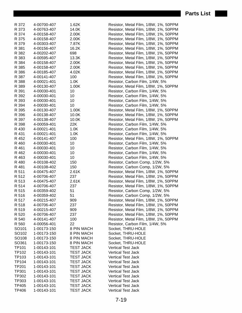
Parts List
7-19
R 372 4-00700-407 1.62K Resistor, Metal Film, 1/8W, 1%, 50PPM R 373 4-00763-407 14.0K Resistor, Metal Film, 1/8W, 1%, 50PPM R 374 4-00158-407 2.00K Resistor, Metal Film, 1/8W, 1%, 50PPM R 375 4-00158-407 2.00K Resistor, Metal Film, 1/8W, 1%, 50PPM R 379 4-00303-407 7.87K Resistor, Metal Film, 1/8W, 1%, 50PPM R 381 4-00156-407 16.2K Resistor, Metal Film, 1/8W, 1%, 50PPM R 382 4-00202-407 698 Resistor, Metal Film, 1/8W, 1%, 50PPM R 383 4-00595-407 13.3K Resistor, Metal Film, 1/8W, 1%, 50PPM R 384 4-00158-407 2.00K Resistor, Metal Film, 1/8W, 1%, 50PPM R 385 4-00158-407 2.00K Resistor, Metal Film, 1/8W, 1%, 50PPM R 386 4-00185-407 4.02K Resistor, Metal Film, 1/8W, 1%, 50PPM R 387 4-00141-407 100 Resistor, Metal Film, 1/8W, 1%, 50PPM R 388 4-00021-401 1.0K Resistor, Carbon Film, 1/4W, 5% R 389 4-00130-407 1.00K Resistor, Metal Film, 1/8W, 1%, 50PPM R 391 4-00030-401 10 Resistor, Carbon Film, 1/4W, 5% R 392 4-00030-401 10 Resistor, Carbon Film, 1/4W, 5% R 393 4-00030-401 10 Resistor, Carbon Film, 1/4W, 5% R 394 4-00030-401 10 Resistor, Carbon Film, 1/4W, 5% R 395 4-00130-407 1.00K Resistor, Metal Film, 1/8W, 1%, 50PPM R 396 4-00138-407 10.0K Resistor, Metal Film, 1/8W, 1%, 50PPM R 397 4-00138-407 10.0K Resistor, Metal Film, 1/8W, 1%, 50PPM R 398 4-00059-401 22K Resistor, Carbon Film, 1/4W, 5% R 430 4-00021-401 1.0K Resistor, Carbon Film, 1/4W, 5% R 431 4-00021-401 1.0K Resistor, Carbon Film, 1/4W, 5% R 452 4-00141-407 100 Resistor, Metal Film, 1/8W, 1%, 50PPM R 460 4-00030-401 10 Resistor, Carbon Film, 1/4W, 5% R 461 4-00030-401 10 Resistor, Carbon Film, 1/4W, 5% R 462 4-00030-401 10 Resistor, Carbon Film, 1/4W, 5% R 463 4-00030-401 10 Resistor, Carbon Film, 1/4W, 5% R 480 4-00108-402 150 Resistor, Carbon Comp, 1/2W, 5% R 481 4-00108-402 150 Resistor, Carbon Comp, 1/2W, 5% R 511 4-00475-407 2.61K Resistor, Metal Film, 1/8W, 1%, 50PPM R 512 4-00706-407 237 Resistor, Metal Film, 1/8W, 1%, 50PPM R 513 4-00475-407 2.61K Resistor, Metal Film, 1/8W, 1%, 50PPM R 514 4-00706-407 237 Resistor, Metal Film, 1/8W, 1%, 50PPM R 515 4-00359-402 51 Resistor, Carbon Comp, 1/2W, 5% R 516 4-00359-402 51 Resistor, Carbon Comp, 1/2W, 5% R 517 4-00215-407 909 Resistor, Metal Film, 1/8W, 1%, 50PPM R 518 4-00706-407 237 Resistor, Metal Film, 1/8W, 1%, 50PPM R 519 4-00215-407 909 Resistor, Metal Film, 1/8W, 1%, 50PPM R 520 4-00706-407 237 Resistor, Metal Film, 1/8W, 1%, 50PPM R 540 4-00141-407 100 Resistor, Metal Film, 1/8W, 1%, 50PPM R 560 4-00056-401 22 Resistor, Carbon Film, 1/4W, 5% SO101 1-00173-150 8 PIN MACH Socket, THRU-HOLE SO102 1-00173-150 8 PIN MACH Socket, THRU-HOLE SO108 1-00173-150 8 PIN MACH Socket, THRU-HOLE SO361 1-00173-150 8 PIN MACH Socket, THRU-HOLE TP101 1-00143-101 TEST JACK Vertical Test Jack TP102 1-00143-101 TEST JACK Vertical Test Jack TP103 1-00143-101 TEST JACK Vertical Test Jack TP104 1-00143-101 TEST JACK Vertical Test Jack TP201 1-00143-101 TEST JACK Vertical Test Jack TP301 1-00143-101 TEST JACK Vertical Test Jack TP302 1-00143-101 TEST JACK Vertical Test Jack TP303 1-00143-101 TEST JACK Vertical Test Jack TP405 1-00143-101 TEST JACK Vertical Test Jack TP406 1-00143-101 TEST JACK Vertical Test Jack
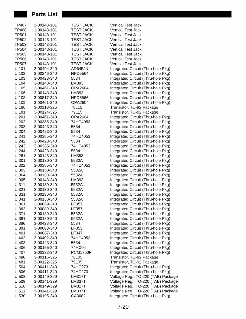
7-20
TP407 1-00143-101 TEST JACK Vertical Test Jack TP408 1-00143-101 TEST JACK Vertical Test Jack TP501 1-00143-101 TEST JACK Vertical Test Jack TP502 1-00143-101 TEST JACK Vertical Test Jack TP503 1-00143-101 TEST JACK Vertical Test Jack TP504 1-00143-101 TEST JACK Vertical Test Jack TP505 1-00143-101 TEST JACK Vertical Test Jack TP506 1-00143-101 TEST JACK Vertical Test Jack TP507 1-00143-101 TEST JACK Vertical Test Jack U 101 3-00494-340 AD645JN Integrated Circuit (Thru-hole Pkg) U 102 3-00246-340 NPD5564 Integrated Circuit (Thru-hole Pkg) U 103 3-00423-340 5534 Integrated Circuit (Thru-hole Pkg) U 104 3-00143-340 LM393 Integrated Circuit (Thru-hole Pkg) U 105 3-00461-340 OPA2604 Integrated Circuit (Thru-hole Pkg) U 106 3-00143-340 LM393 Integrated Circuit (Thru-hole Pkg) U 108 3-00817-340 NPD5566 Integrated Circuit (Thru-hole Pkg) U 109 3-00461-340 OPA2604 Integrated Circuit (Thru-hole Pkg) U 180 3-00118-325 78L15 Transistor, TO-92 Package U 181 3-00124-325 79L15 Transistor, TO-92 Package U 201 3-00461-340 OPA2604 Integrated Circuit (Thru-hole Pkg) U 202 3-00385-340 74HC4053 Integrated Circuit (Thru-hole Pkg) U 203 3-00423-340 5534 Integrated Circuit (Thru-hole Pkg) U 204 3-00423-340 5534 Integrated Circuit (Thru-hole Pkg) U 241 3-00385-340 74HC4053 Integrated Circuit (Thru-hole Pkg) U 242 3-00423-340 5534 Integrated Circuit (Thru-hole Pkg) U 243 3-00385-340 74HC4053 Integrated Circuit (Thru-hole Pkg) U 244 3-00423-340 5534 Integrated Circuit (Thru-hole Pkg) U 261 3-00143-340 LM393 Integrated Circuit (Thru-hole Pkg) U 301 3-00130-340 5532A Integrated Circuit (Thru-hole Pkg) U 302 3-00385-340 74HC4053 Integrated Circuit (Thru-hole Pkg) U 303 3-00130-340 5532A Integrated Circuit (Thru-hole Pkg) U 304 3-00130-340 5532A Integrated Circuit (Thru-hole Pkg) U 305 3-00143-340 LM393 Integrated Circuit (Thru-hole Pkg) U 311 3-00130-340 5532A Integrated Circuit (Thru-hole Pkg) U 321 3-00130-340 5532A Integrated Circuit (Thru-hole Pkg) U 331 3-00130-340 5532A Integrated Circuit (Thru-hole Pkg) U 341 3-00130-340 5532A Integrated Circuit (Thru-hole Pkg) U 361 3-00089-340 LF357 Integrated Circuit (Thru-hole Pkg) U 362 3-00089-340 LF357 Integrated Circuit (Thru-hole Pkg) U 371 3-00130-340 5532A Integrated Circuit (Thru-hole Pkg) U 381 3-00130-340 5532A Integrated Circuit (Thru-hole Pkg) U 386 3-00423-340 5534 Integrated Circuit (Thru-hole Pkg) U 391 3-00088-340 LF353 Integrated Circuit (Thru-hole Pkg) U 401 3-00087-340 LF347 Integrated Circuit (Thru-hole Pkg) U 402 3-00402-340 74HC4052 Integrated Circuit (Thru-hole Pkg) U 403 3-00423-340 5534 Integrated Circuit (Thru-hole Pkg) U 406 3-00155-340 74HC04 Integrated Circuit (Thru-hole Pkg) U 407 3-00392-340 PCM1750P Integrated Circuit (Thru-hole Pkg) U 480 3-00116-325 78L05 Transistor, TO-92 Package U 481 3-00122-325 79L05 Transistor, TO-92 Package U 504 3-00411-340 74HC273 Integrated Circuit (Thru-hole Pkg) U 506 3-00411-340 74HC273 Integrated Circuit (Thru-hole Pkg) U 508 3-00149-329 LM317T Voltage Reg., TO-220 (TAB) Package U 509 3-00141-329 LM337T Voltage Reg., TO-220 (TAB) Package U 510 3-00149-329 LM317T Voltage Reg., TO-220 (TAB) Package U 511 3-00141-329 LM337T Voltage Reg., TO-220 (TAB) Package U 530 3-00195-340 CA3082 Integrated Circuit (Thru-hole Pkg)
Parts List
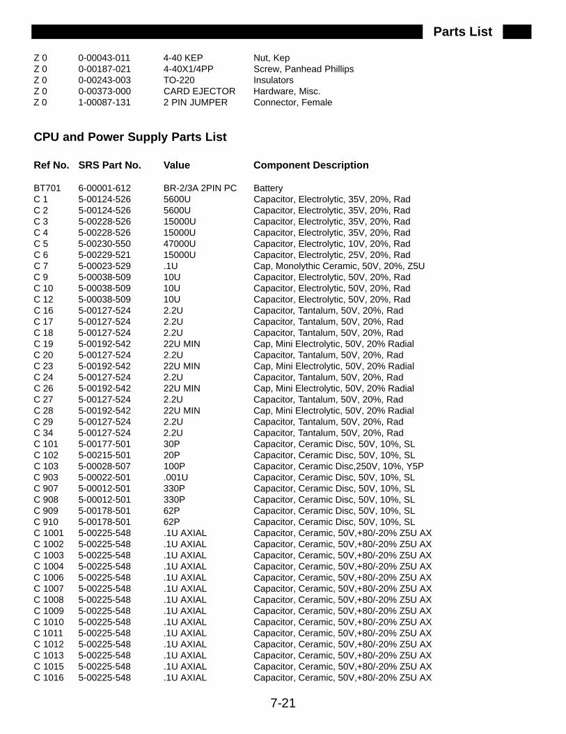
7-21
Z 0 0-00043-011 4-40 KEP Nut, Kep Z 0 0-00187-021 4-40X1/4PP Screw, Panhead Phillips Z 0 0-00243-003 TO-220 Insulators Z 0 0-00373-000 CARD EJECTOR Hardware, Misc. Z 0 1-00087-131 2 PIN JUMPER Connector, Female
CPU and Power Supply Parts List
Ref No. SRS Part No. Value Component Description
BT701 6-00001-612 BR-2/3A 2PIN PC Battery C 1 5-00124-526 5600U Capacitor, Electrolytic, 35V, 20%, Rad C 2 5-00124-526 5600U Capacitor, Electrolytic, 35V, 20%, Rad C 3 5-00228-526 15000U Capacitor, Electrolytic, 35V, 20%, Rad C 4 5-00228-526 15000U Capacitor, Electrolytic, 35V, 20%, Rad C 5 5-00230-550 47000U Capacitor, Electrolytic, 10V, 20%, Rad C 6 5-00229-521 15000U Capacitor, Electrolytic, 25V, 20%, Rad C 7 5-00023-529 .1U Cap, Monolythic Ceramic, 50V, 20%, Z5U C 9 5-00038-509 10U Capacitor, Electrolytic, 50V, 20%, Rad C 10 5-00038-509 10U Capacitor, Electrolytic, 50V, 20%, Rad C 12 5-00038-509 10U Capacitor, Electrolytic, 50V, 20%, Rad C 16 5-00127-524 2.2U Capacitor, Tantalum, 50V, 20%, Rad C 17 5-00127-524 2.2U Capacitor, Tantalum, 50V, 20%, Rad C 18 5-00127-524 2.2U Capacitor, Tantalum, 50V, 20%, Rad C 19 5-00192-542 22U MIN Cap, Mini Electrolytic, 50V, 20% Radial C 20 5-00127-524 2.2U Capacitor, Tantalum, 50V, 20%, Rad C 23 5-00192-542 22U MIN Cap, Mini Electrolytic, 50V, 20% Radial C 24 5-00127-524 2.2U Capacitor, Tantalum, 50V, 20%, Rad C 26 5-00192-542 22U MIN Cap, Mini Electrolytic, 50V, 20% Radial C 27 5-00127-524 2.2U Capacitor, Tantalum, 50V, 20%, Rad C 28 5-00192-542 22U MIN Cap, Mini Electrolytic, 50V, 20% Radial C 29 5-00127-524 2.2U Capacitor, Tantalum, 50V, 20%, Rad C 34 5-00127-524 2.2U Capacitor, Tantalum, 50V, 20%, Rad C 101 5-00177-501 30P Capacitor, Ceramic Disc, 50V, 10%, SLC 102 5-00215-501 20P Capacitor, Ceramic Disc, 50V, 10%, SLC 103 5-00028-507 100P Capacitor, Ceramic Disc,250V, 10%, Y5PC 903 5-00022-501 .001U Capacitor, Ceramic Disc, 50V, 10%, SLC 907 5-00012-501 330P Capacitor, Ceramic Disc, 50V, 10%, SLC 908 5-00012-501 330P Capacitor, Ceramic Disc, 50V, 10%, SLC 909 5-00178-501 62P Capacitor, Ceramic Disc, 50V, 10%, SLC 910 5-00178-501 62P Capacitor, Ceramic Disc, 50V, 10%, SLC 1001 5-00225-548 .1U AXIAL Capacitor, Ceramic, 50V,+80/-20% Z5U AX C 1002 5-00225-548 .1U AXIAL Capacitor, Ceramic, 50V,+80/-20% Z5U AX C 1003 5-00225-548 .1U AXIAL Capacitor, Ceramic, 50V,+80/-20% Z5U AX C 1004 5-00225-548 .1U AXIAL Capacitor, Ceramic, 50V,+80/-20% Z5U AX C 1006 5-00225-548 .1U AXIAL Capacitor, Ceramic, 50V,+80/-20% Z5U AX C 1007 5-00225-548 .1U AXIAL Capacitor, Ceramic, 50V,+80/-20% Z5U AX C 1008 5-00225-548 .1U AXIAL Capacitor, Ceramic, 50V,+80/-20% Z5U AX C 1009 5-00225-548 .1U AXIAL Capacitor, Ceramic, 50V,+80/-20% Z5U AX C 1010 5-00225-548 .1U AXIAL Capacitor, Ceramic, 50V,+80/-20% Z5U AX C 1011 5-00225-548 .1U AXIAL Capacitor, Ceramic, 50V,+80/-20% Z5U AX C 1012 5-00225-548 .1U AXIAL Capacitor, Ceramic, 50V,+80/-20% Z5U AX C 1013 5-00225-548 .1U AXIAL Capacitor, Ceramic, 50V,+80/-20% Z5U AX C 1015 5-00225-548 .1U AXIAL Capacitor, Ceramic, 50V,+80/-20% Z5U AX C 1016 5-00225-548 .1U AXIAL Capacitor, Ceramic, 50V,+80/-20% Z5U AX
Parts List
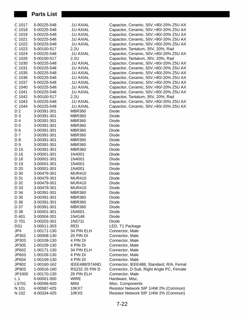
7-22
C 1017 5-00225-548 .1U AXIAL Capacitor, Ceramic, 50V,+80/-20% Z5U AX C 1018 5-00225-548 .1U AXIAL Capacitor, Ceramic, 50V,+80/-20% Z5U AX C 1019 5-00225-548 .1U AXIAL Capacitor, Ceramic, 50V,+80/-20% Z5U AX C 1021 5-00225-548 .1U AXIAL Capacitor, Ceramic, 50V,+80/-20% Z5U AX C 1022 5-00225-548 .1U AXIAL Capacitor, Ceramic, 50V,+80/-20% Z5U AX C 1023 5-00100-517 2.2U Capacitor, Tantalum, 35V, 20%, Rad C 1024 5-00225-548 .1U AXIAL Capacitor, Ceramic, 50V,+80/-20% Z5U AX C 1026 5-00100-517 2.2U Capacitor, Tantalum, 35V, 20%, Rad C 1030 5-00225-548 .1U AXIAL Capacitor, Ceramic, 50V,+80/-20% Z5U AX C 1031 5-00225-548 .1U AXIAL Capacitor, Ceramic, 50V,+80/-20% Z5U AX C 1035 5-00225-548 .1U AXIAL Capacitor, Ceramic, 50V,+80/-20% Z5U AX C 1036 5-00225-548 .1U AXIAL Capacitor, Ceramic, 50V,+80/-20% Z5U AX C 1037 5-00225-548 .1U AXIAL Capacitor, Ceramic, 50V,+80/-20% Z5U AX C 1040 5-00225-548 .1U AXIAL Capacitor, Ceramic, 50V,+80/-20% Z5U AX C 1041 5-00225-548 .1U AXIAL Capacitor, Ceramic, 50V,+80/-20% Z5U AX C 1042 5-00100-517 2.2U Capacitor, Tantalum, 35V, 20%, Rad C 1043 5-00225-548 .1U AXIAL Capacitor, Ceramic, 50V,+80/-20% Z5U AX C 1044 5-00225-548 .1U AXIAL Capacitor, Ceramic, 50V,+80/-20% Z5U AX D 2 3-00391-301 MBR360 Diode D 3 3-00391-301 MBR360 Diode D 4 3-00391-301 MBR360 Diode D 5 3-00391-301 MBR360 Diode D 6 3-00391-301 MBR360 Diode D 7 3-00391-301 MBR360 Diode D 8 3-00391-301 MBR360 Diode D 9 3-00391-301 MBR360 Diode D 15 3-00391-301 MBR360 Diode D 16 3-00001-301 1N4001 Diode D 18 3-00001-301 1N4001 Diode D 19 3-00001-301 1N4001 Diode D 20 3-00001-301 1N4001 Diode D 30 3-00479-301 MUR410 Diode D 31 3-00479-301 MUR410 Diode D 32 3-00479-301 MUR410 Diode D 33 3-00479-301 MUR410 Diode D 34 3-00391-301 MBR360 Diode D 35 3-00391-301 MBR360 Diode D 36 3-00391-301 MBR360 Diode D 37 3-00391-301 MBR360 Diode D 38 3-00001-301 1N4001 Diode D 401 3-00004-301 1N4148 Diode D 701 3-00203-301 1N5711 Diode DS1 3-00011-303 RED LED, T1 Package JP4 1-00171-130 34 PIN ELH Connector, Male JP302 1-00008-130 20 PIN DI Connector, Male JP303 1-00109-130 4 PIN DI Connector, Male JP305 1-00109-130 4 PIN DI Connector, Male JP602 1-00171-130 34 PIN ELH Connector, Male JP603 1-00109-130 4 PIN DI Connector, Male JP604 1-00109-130 4 PIN DI Connector, Male JP902 1-00160-162 IEEE488/STAND. Connector, IEEE488, Standard, R/A, FemalJP903 1-00016-160 RS232 25 PIN D Connector, D-Sub, Right Angle PC, FemaleJP1000 1-00170-130 26 PIN ELH Connector, Male L 1 0-00001-000 WIRE Hardware, Misc. LS701 6-00096-600 MINI Misc. Components N 101 4-00587-425 10KX7 Resistor Network SIP 1/4W 2% (Common) N 102 4-00334-425 10KX5 Resistor Network SIP 1/4W 2% (Common)
Parts List
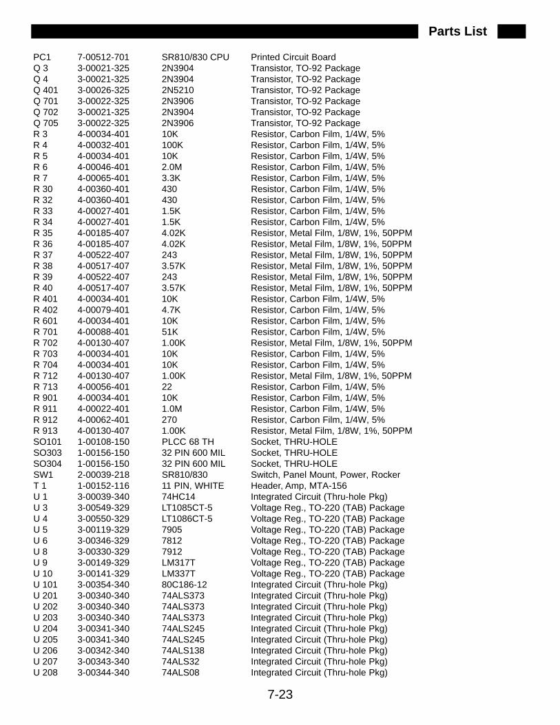
7-23
PC1 7-00512-701 SR810/830 CPU Printed Circuit Board Q 3 3-00021-325 2N3904 Transistor, TO-92 Package Q 4 3-00021-325 2N3904 Transistor, TO-92 Package Q 401 3-00026-325 2N5210 Transistor, TO-92 Package Q 701 3-00022-325 2N3906 Transistor, TO-92 Package Q 702 3-00021-325 2N3904 Transistor, TO-92 Package Q 705 3-00022-325 2N3906 Transistor, TO-92 Package R 3 4-00034-401 10K Resistor, Carbon Film, 1/4W, 5% R 4 4-00032-401 100K Resistor, Carbon Film, 1/4W, 5% R 5 4-00034-401 10K Resistor, Carbon Film, 1/4W, 5% R 6 4-00046-401 2.0M Resistor, Carbon Film, 1/4W, 5% R 7 4-00065-401 3.3K Resistor, Carbon Film, 1/4W, 5% R 30 4-00360-401 430 Resistor, Carbon Film, 1/4W, 5% R 32 4-00360-401 430 Resistor, Carbon Film, 1/4W, 5% R 33 4-00027-401 1.5K Resistor, Carbon Film, 1/4W, 5% R 34 4-00027-401 1.5K Resistor, Carbon Film, 1/4W, 5% R 35 4-00185-407 4.02K Resistor, Metal Film, 1/8W, 1%, 50PPM R 36 4-00185-407 4.02K Resistor, Metal Film, 1/8W, 1%, 50PPM R 37 4-00522-407 243 Resistor, Metal Film, 1/8W, 1%, 50PPM R 38 4-00517-407 3.57K Resistor, Metal Film, 1/8W, 1%, 50PPM R 39 4-00522-407 243 Resistor, Metal Film, 1/8W, 1%, 50PPM R 40 4-00517-407 3.57K Resistor, Metal Film, 1/8W, 1%, 50PPM R 401 4-00034-401 10K Resistor, Carbon Film, 1/4W, 5% R 402 4-00079-401 4.7K Resistor, Carbon Film, 1/4W, 5% R 601 4-00034-401 10K Resistor, Carbon Film, 1/4W, 5% R 701 4-00088-401 51K Resistor, Carbon Film, 1/4W, 5% R 702 4-00130-407 1.00K Resistor, Metal Film, 1/8W, 1%, 50PPM R 703 4-00034-401 10K Resistor, Carbon Film, 1/4W, 5% R 704 4-00034-401 10K Resistor, Carbon Film, 1/4W, 5% R 712 4-00130-407 1.00K Resistor, Metal Film, 1/8W, 1%, 50PPM R 713 4-00056-401 22 Resistor, Carbon Film, 1/4W, 5% R 901 4-00034-401 10K Resistor, Carbon Film, 1/4W, 5% R 911 4-00022-401 1.0M Resistor, Carbon Film, 1/4W, 5% R 912 4-00062-401 270 Resistor, Carbon Film, 1/4W, 5% R 913 4-00130-407 1.00K Resistor, Metal Film, 1/8W, 1%, 50PPM SO101 1-00108-150 PLCC 68 TH Socket, THRU-HOLE SO303 1-00156-150 32 PIN 600 MIL Socket, THRU-HOLE SO304 1-00156-150 32 PIN 600 MIL Socket, THRU-HOLE SW1 2-00039-218 SR810/830 Switch, Panel Mount, Power, Rocker T 1 1-00152-116 11 PIN, WHITE Header, Amp, MTA-156 U 1 3-00039-340 74HC14 Integrated Circuit (Thru-hole Pkg) U 3 3-00549-329 LT1085CT-5 Voltage Reg., TO-220 (TAB) Package U 4 3-00550-329 LT1086CT-5 Voltage Reg., TO-220 (TAB) Package U 5 3-00119-329 7905 Voltage Reg., TO-220 (TAB) Package U 6 3-00346-329 7812 Voltage Reg., TO-220 (TAB) Package U 8 3-00330-329 7912 Voltage Reg., TO-220 (TAB) Package U 9 3-00149-329 LM317T Voltage Reg., TO-220 (TAB) Package U 10 3-00141-329 LM337T Voltage Reg., TO-220 (TAB) Package U 101 3-00354-340 80C186-12 Integrated Circuit (Thru-hole Pkg) U 201 3-00340-340 74ALS373 Integrated Circuit (Thru-hole Pkg) U 202 3-00340-340 74ALS373 Integrated Circuit (Thru-hole Pkg) U 203 3-00340-340 74ALS373 Integrated Circuit (Thru-hole Pkg) U 204 3-00341-340 74ALS245 Integrated Circuit (Thru-hole Pkg) U 205 3-00341-340 74ALS245 Integrated Circuit (Thru-hole Pkg) U 206 3-00342-340 74ALS138 Integrated Circuit (Thru-hole Pkg) U 207 3-00343-340 74ALS32 Integrated Circuit (Thru-hole Pkg) U 208 3-00344-340 74ALS08 Integrated Circuit (Thru-hole Pkg)
Parts List
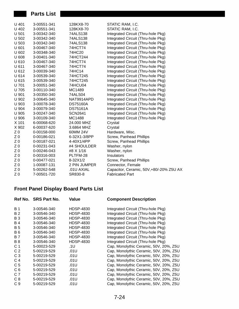
7-24
U 401 3-00551-341 128KX8-70 STATIC RAM, I.C. U 402 3-00551-341 128KX8-70 STATIC RAM, I.C. U 501 3-00342-340 74ALS138 Integrated Circuit (Thru-hole Pkg) U 502 3-00342-340 74ALS138 Integrated Circuit (Thru-hole Pkg) U 503 3-00342-340 74ALS138 Integrated Circuit (Thru-hole Pkg) U 601 3-00467-340 74HCT74 Integrated Circuit (Thru-hole Pkg) U 602 3-00348-340 74HC20 Integrated Circuit (Thru-hole Pkg) U 608 3-00401-340 74HCT244 Integrated Circuit (Thru-hole Pkg) U 610 3-00467-340 74HCT74 Integrated Circuit (Thru-hole Pkg) U 611 3-00467-340 74HCT74 Integrated Circuit (Thru-hole Pkg) U 612 3-00039-340 74HC14 Integrated Circuit (Thru-hole Pkg) U 614 3-00539-340 74HCT245 Integrated Circuit (Thru-hole Pkg) U 615 3-00539-340 74HCT245 Integrated Circuit (Thru-hole Pkg) U 701 3-00051-340 74HCU04 Integrated Circuit (Thru-hole Pkg) U 705 3-00110-340 MC1489 Integrated Circuit (Thru-hole Pkg) U 901 3-00350-340 74ALS04 Integrated Circuit (Thru-hole Pkg) U 902 3-00645-340 NAT9914APD Integrated Circuit (Thru-hole Pkg) U 903 3-00078-340 DS75160A Integrated Circuit (Thru-hole Pkg) U 904 3-00079-340 DS75161A Integrated Circuit (Thru-hole Pkg) U 905 3-00247-340 SCN2641 Integrated Circuit (Thru-hole Pkg) U 906 3-00109-340 MC1488 Integrated Circuit (Thru-hole Pkg) X 101 6-00068-620 24.000 MHZ Crystal X 902 6-00037-620 3.6864 MHZ Crystal Z 0 0-00158-000 60MM 24V Hardware, Misc. Z 0 0-00186-021 6-32X1-3/8PP Screw, Panhead Phillips Z 0 0-00187-021 4-40X1/4PP Screw, Panhead Phillips Z 0 0-00231-043 #4 SHOULDER Washer, nylon Z 0 0-00246-043 #8 X 1/16 Washer, nylon Z 0 0-00316-003 PLTFM-28 Insulators Z 0 0-00477-021 8-32X1/2 Screw, Panhead Phillips Z 0 1-00087-131 2 PIN JUMPER Connector, Female Z 0 5-00262-548 .01U AXIAL Capacitor, Ceramic, 50V,+80/-20% Z5U AX Z 0 7-00501-720 SR830-8 Fabricated Part
Front Panel Display Board Parts List
Ref No. SRS Part No. Value Component Description
B 1 3-00546-340 HDSP-4830 Integrated Circuit (Thru-hole Pkg) B 2 3-00546-340 HDSP-4830 Integrated Circuit (Thru-hole Pkg) B 3 3-00546-340 HDSP-4830 Integrated Circuit (Thru-hole Pkg) B 4 3-00546-340 HDSP-4830 Integrated Circuit (Thru-hole Pkg) B 5 3-00546-340 HDSP-4830 Integrated Circuit (Thru-hole Pkg) B 6 3-00546-340 HDSP-4830 Integrated Circuit (Thru-hole Pkg) B 7 3-00546-340 HDSP-4830 Integrated Circuit (Thru-hole Pkg) B 8 3-00546-340 HDSP-4830 Integrated Circuit (Thru-hole Pkg) C 1 5-00023-529 .1U Cap, Monolythic Ceramic, 50V, 20%, Z5U C 2 5-00219-529 .01U Cap, Monolythic Ceramic, 50V, 20%, Z5U C 3 5-00219-529 .01U Cap, Monolythic Ceramic, 50V, 20%, Z5U C 4 5-00219-529 .01U Cap, Monolythic Ceramic, 50V, 20%, Z5U C 5 5-00219-529 .01U Cap, Monolythic Ceramic, 50V, 20%, Z5U C 6 5-00219-529 .01U Cap, Monolythic Ceramic, 50V, 20%, Z5U C 7 5-00219-529 .01U Cap, Monolythic Ceramic, 50V, 20%, Z5U C 8 5-00219-529 .01U Cap, Monolythic Ceramic, 50V, 20%, Z5U C 9 5-00219-529 .01U Cap, Monolythic Ceramic, 50V, 20%, Z5U
Parts List
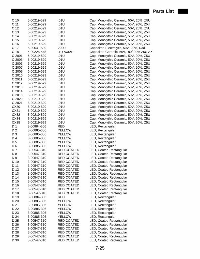
7-25
C 10 5-00219-529 .01U Cap, Monolythic Ceramic, 50V, 20%, Z5U C 11 5-00219-529 .01U Cap, Monolythic Ceramic, 50V, 20%, Z5U C 12 5-00219-529 .01U Cap, Monolythic Ceramic, 50V, 20%, Z5U C 13 5-00219-529 .01U Cap, Monolythic Ceramic, 50V, 20%, Z5U C 14 5-00219-529 .01U Cap, Monolythic Ceramic, 50V, 20%, Z5U C 15 5-00219-529 .01U Cap, Monolythic Ceramic, 50V, 20%, Z5U C 16 5-00219-529 .01U Cap, Monolythic Ceramic, 50V, 20%, Z5U C 17 5-00041-509 220U Capacitor, Electrolytic, 50V, 20%, Rad C 18 5-00225-548 .1U AXIAL Capacitor, Ceramic, 50V,+80/-20% Z5U AX C 2001 5-00219-529 .01U Cap, Monolythic Ceramic, 50V, 20%, Z5U C 2003 5-00219-529 .01U Cap, Monolythic Ceramic, 50V, 20%, Z5U C 2005 5-00219-529 .01U Cap, Monolythic Ceramic, 50V, 20%, Z5U C 2007 5-00219-529 .01U Cap, Monolythic Ceramic, 50V, 20%, Z5U C 2009 5-00219-529 .01U Cap, Monolythic Ceramic, 50V, 20%, Z5U C 2010 5-00219-529 .01U Cap, Monolythic Ceramic, 50V, 20%, Z5U C 2011 5-00219-529 .01U Cap, Monolythic Ceramic, 50V, 20%, Z5U C 2012 5-00219-529 .01U Cap, Monolythic Ceramic, 50V, 20%, Z5U C 2013 5-00219-529 .01U Cap, Monolythic Ceramic, 50V, 20%, Z5U C 2014 5-00219-529 .01U Cap, Monolythic Ceramic, 50V, 20%, Z5U C 2015 5-00219-529 .01U Cap, Monolythic Ceramic, 50V, 20%, Z5U C 2020 5-00219-529 .01U Cap, Monolythic Ceramic, 50V, 20%, Z5U C 2021 5-00219-529 .01U Cap, Monolythic Ceramic, 50V, 20%, Z5U CX30 5-00219-529 .01U Cap, Monolythic Ceramic, 50V, 20%, Z5U CX31 5-00219-529 .01U Cap, Monolythic Ceramic, 50V, 20%, Z5U CX32 5-00219-529 .01U Cap, Monolythic Ceramic, 50V, 20%, Z5U CX34 5-00219-529 .01U Cap, Monolythic Ceramic, 50V, 20%, Z5U CX35 5-00219-529 .01U Cap, Monolythic Ceramic, 50V, 20%, Z5U D 1 3-00884-306 RED LED, Rectangular D 2 3-00885-306 YELLOW LED, Rectangular D 3 3-00885-306 YELLOW LED, Rectangular D 4 3-00885-306 YELLOW LED, Rectangular D 5 3-00885-306 YELLOW LED, Rectangular D 6 3-00885-306 YELLOW LED, Rectangular D 7 3-00547-310 RED COATED LED, Coated Rectangular D 8 3-00547-310 RED COATED LED, Coated Rectangular D 9 3-00547-310 RED COATED LED, Coated Rectangular D 10 3-00547-310 RED COATED LED, Coated Rectangular D 11 3-00547-310 RED COATED LED, Coated Rectangular D 12 3-00547-310 RED COATED LED, Coated Rectangular D 13 3-00547-310 RED COATED LED, Coated Rectangular D 14 3-00547-310 RED COATED LED, Coated Rectangular D 15 3-00547-310 RED COATED LED, Coated Rectangular D 16 3-00547-310 RED COATED LED, Coated Rectangular D 17 3-00547-310 RED COATED LED, Coated Rectangular D 18 3-00547-310 RED COATED LED, Coated Rectangular D 19 3-00884-306 RED LED, Rectangular D 20 3-00885-306 YELLOW LED, Rectangular D 21 3-00885-306 YELLOW LED, Rectangular D 22 3-00885-306 YELLOW LED, Rectangular D 23 3-00885-306 YELLOW LED, Rectangular D 24 3-00885-306 YELLOW LED, Rectangular D 25 3-00547-310 RED COATED LED, Coated Rectangular D 26 3-00547-310 RED COATED LED, Coated Rectangular D 27 3-00547-310 RED COATED LED, Coated Rectangular D 28 3-00547-310 RED COATED LED, Coated Rectangular D 29 3-00547-310 RED COATED LED, Coated Rectangular D 30 3-00547-310 RED COATED LED, Coated Rectangular
Parts List
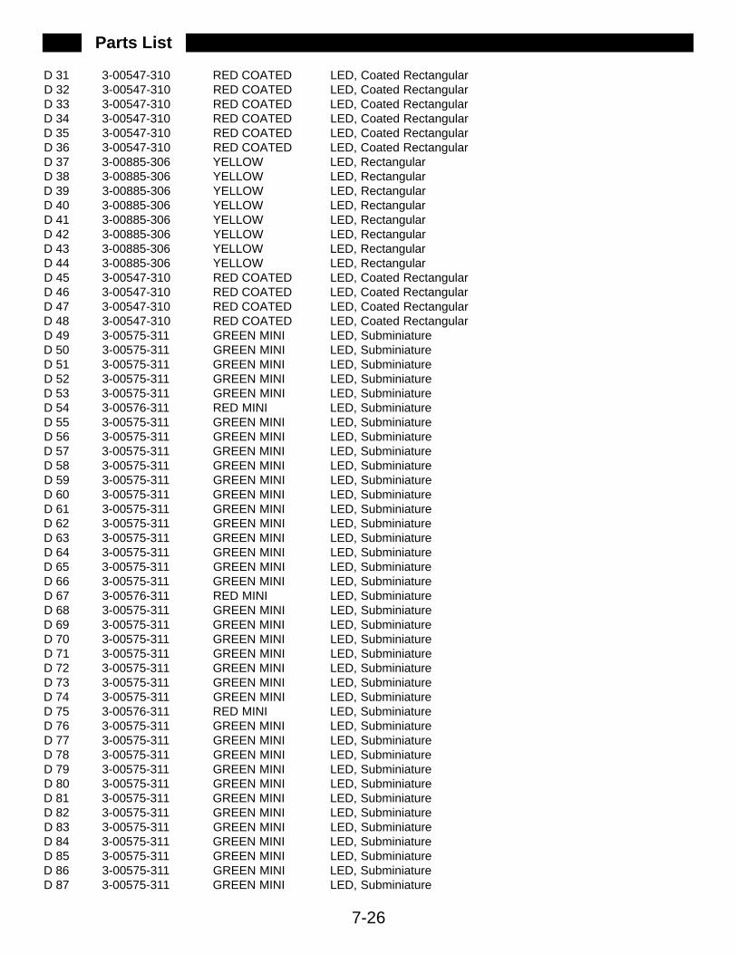
7-26
D 31 3-00547-310 RED COATED LED, Coated Rectangular D 32 3-00547-310 RED COATED LED, Coated Rectangular D 33 3-00547-310 RED COATED LED, Coated Rectangular D 34 3-00547-310 RED COATED LED, Coated Rectangular D 35 3-00547-310 RED COATED LED, Coated Rectangular D 36 3-00547-310 RED COATED LED, Coated Rectangular D 37 3-00885-306 YELLOW LED, Rectangular D 38 3-00885-306 YELLOW LED, Rectangular D 39 3-00885-306 YELLOW LED, Rectangular D 40 3-00885-306 YELLOW LED, Rectangular D 41 3-00885-306 YELLOW LED, Rectangular D 42 3-00885-306 YELLOW LED, Rectangular D 43 3-00885-306 YELLOW LED, Rectangular D 44 3-00885-306 YELLOW LED, Rectangular D 45 3-00547-310 RED COATED LED, Coated Rectangular D 46 3-00547-310 RED COATED LED, Coated Rectangular D 47 3-00547-310 RED COATED LED, Coated Rectangular D 48 3-00547-310 RED COATED LED, Coated Rectangular D 49 3-00575-311 GREEN MINI LED, Subminiature D 50 3-00575-311 GREEN MINI LED, Subminiature D 51 3-00575-311 GREEN MINI LED, Subminiature D 52 3-00575-311 GREEN MINI LED, Subminiature D 53 3-00575-311 GREEN MINI LED, Subminiature D 54 3-00576-311 RED MINI LED, Subminiature D 55 3-00575-311 GREEN MINI LED, Subminiature D 56 3-00575-311 GREEN MINI LED, Subminiature D 57 3-00575-311 GREEN MINI LED, Subminiature D 58 3-00575-311 GREEN MINI LED, Subminiature D 59 3-00575-311 GREEN MINI LED, Subminiature D 60 3-00575-311 GREEN MINI LED, Subminiature D 61 3-00575-311 GREEN MINI LED, Subminiature D 62 3-00575-311 GREEN MINI LED, Subminiature D 63 3-00575-311 GREEN MINI LED, Subminiature D 64 3-00575-311 GREEN MINI LED, Subminiature D 65 3-00575-311 GREEN MINI LED, Subminiature D 66 3-00575-311 GREEN MINI LED, Subminiature D 67 3-00576-311 RED MINI LED, Subminiature D 68 3-00575-311 GREEN MINI LED, Subminiature D 69 3-00575-311 GREEN MINI LED, Subminiature D 70 3-00575-311 GREEN MINI LED, Subminiature D 71 3-00575-311 GREEN MINI LED, Subminiature D 72 3-00575-311 GREEN MINI LED, Subminiature D 73 3-00575-311 GREEN MINI LED, Subminiature D 74 3-00575-311 GREEN MINI LED, Subminiature D 75 3-00576-311 RED MINI LED, Subminiature D 76 3-00575-311 GREEN MINI LED, Subminiature D 77 3-00575-311 GREEN MINI LED, Subminiature D 78 3-00575-311 GREEN MINI LED, Subminiature D 79 3-00575-311 GREEN MINI LED, Subminiature D 80 3-00575-311 GREEN MINI LED, Subminiature D 81 3-00575-311 GREEN MINI LED, Subminiature D 82 3-00575-311 GREEN MINI LED, Subminiature D 83 3-00575-311 GREEN MINI LED, Subminiature D 84 3-00575-311 GREEN MINI LED, Subminiature D 85 3-00575-311 GREEN MINI LED, Subminiature D 86 3-00575-311 GREEN MINI LED, Subminiature D 87 3-00575-311 GREEN MINI LED, Subminiature
Parts List
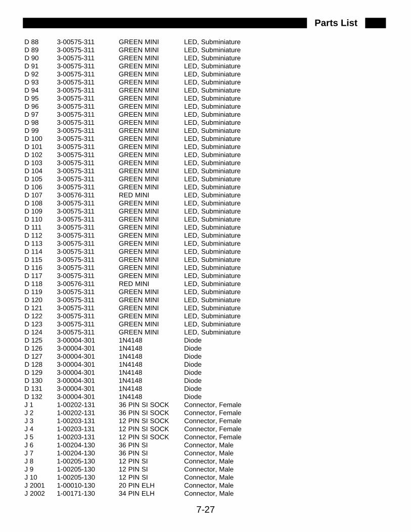
7-27
D 88 3-00575-311 GREEN MINI LED, Subminiature D 89 3-00575-311 GREEN MINI LED, Subminiature D 90 3-00575-311 GREEN MINI LED, Subminiature D 91 3-00575-311 GREEN MINI LED, Subminiature D 92 3-00575-311 GREEN MINI LED, Subminiature D 93 3-00575-311 GREEN MINI LED, Subminiature D 94 3-00575-311 GREEN MINI LED, Subminiature D 95 3-00575-311 GREEN MINI LED, Subminiature D 96 3-00575-311 GREEN MINI LED, Subminiature D 97 3-00575-311 GREEN MINI LED, Subminiature D 98 3-00575-311 GREEN MINI LED, Subminiature D 99 3-00575-311 GREEN MINI LED, Subminiature D 100 3-00575-311 GREEN MINI LED, Subminiature D 101 3-00575-311 GREEN MINI LED, Subminiature D 102 3-00575-311 GREEN MINI LED, Subminiature D 103 3-00575-311 GREEN MINI LED, Subminiature D 104 3-00575-311 GREEN MINI LED, Subminiature D 105 3-00575-311 GREEN MINI LED, Subminiature D 106 3-00575-311 GREEN MINI LED, Subminiature D 107 3-00576-311 RED MINI LED, Subminiature D 108 3-00575-311 GREEN MINI LED, Subminiature D 109 3-00575-311 GREEN MINI LED, Subminiature D 110 3-00575-311 GREEN MINI LED, Subminiature D 111 3-00575-311 GREEN MINI LED, Subminiature D 112 3-00575-311 GREEN MINI LED, Subminiature D 113 3-00575-311 GREEN MINI LED, Subminiature D 114 3-00575-311 GREEN MINI LED, Subminiature D 115 3-00575-311 GREEN MINI LED, Subminiature D 116 3-00575-311 GREEN MINI LED, Subminiature D 117 3-00575-311 GREEN MINI LED, Subminiature D 118 3-00576-311 RED MINI LED, Subminiature D 119 3-00575-311 GREEN MINI LED, Subminiature D 120 3-00575-311 GREEN MINI LED, Subminiature D 121 3-00575-311 GREEN MINI LED, Subminiature D 122 3-00575-311 GREEN MINI LED, Subminiature D 123 3-00575-311 GREEN MINI LED, Subminiature D 124 3-00575-311 GREEN MINI LED, Subminiature D 125 3-00004-301 1N4148 Diode D 126 3-00004-301 1N4148 Diode D 127 3-00004-301 1N4148 Diode D 128 3-00004-301 1N4148 Diode D 129 3-00004-301 1N4148 Diode D 130 3-00004-301 1N4148 Diode D 131 3-00004-301 1N4148 Diode D 132 3-00004-301 1N4148 Diode J 1 1-00202-131 36 PIN SI SOCK Connector, Female J 2 1-00202-131 36 PIN SI SOCK Connector, Female J 3 1-00203-131 12 PIN SI SOCK Connector, Female J 4 1-00203-131 12 PIN SI SOCK Connector, Female J 5 1-00203-131 12 PIN SI SOCK Connector, Female J 6 1-00204-130 36 PIN SI Connector, Male J 7 1-00204-130 36 PIN SI Connector, Male J 8 1-00205-130 12 PIN SI Connector, Male J 9 1-00205-130 12 PIN SI Connector, Male J 10 1-00205-130 12 PIN SI Connector, Male J 2001 1-00010-130 20 PIN ELH Connector, Male J 2002 1-00171-130 34 PIN ELH Connector, Male
Parts List
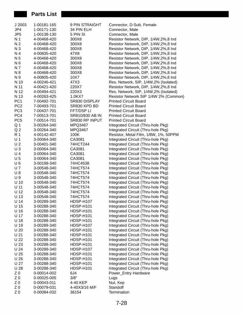
7-28
J 2003 1-00181-165 9 PIN STRAIGHT Connector, D-Sub, Female JP4 1-00171-130 34 PIN ELH Connector, Male JP5 1-00138-130 5 PIN SI Connector, Male N 1 4-00468-420 300X8 Resistor Network, DIP, 1/4W,2%,8 Ind N 2 4-00468-420 300X8 Resistor Network, DIP, 1/4W,2%,8 Ind N 3 4-00468-420 300X8 Resistor Network, DIP, 1/4W,2%,8 Ind N 4 4-00835-420 47X8 Resistor Network, DIP, 1/4W,2%,8 Ind N 5 4-00468-420 300X8 Resistor Network, DIP, 1/4W,2%,8 Ind N 6 4-00468-420 300X8 Resistor Network, DIP, 1/4W,2%,8 Ind N 7 4-00468-420 300X8 Resistor Network, DIP, 1/4W,2%,8 Ind N 8 4-00468-420 300X8 Resistor Network, DIP, 1/4W,2%,8 Ind N 9 4-00805-420 10X7 Resistor Network, DIP, 1/4W,2%,8 Ind N 10 4-00246-421 47X3 Res. Network, SIP, 1/4W,2% (Isolated) N 11 4-00421-420 220X7 Resistor Network, DIP, 1/4W,2%,8 Ind N 12 4-00494-421 220X3 Res. Network, SIP, 1/4W,2% (Isolated) N 13 4-00263-425 1.0KX7 Resistor Network SIP 1/4W 2% (Common) PC1 7-00492-701 SR830 DISPLAY Printed Circuit Board PC2 7-00493-701 SR830 KPD BD Printed Circuit Board PC3 7-00437-701 FFT/DSP LI Printed Circuit Board PC4 7-00513-701 SR810/830 AB IN Printed Circuit Board PC5 7-00514-701 SR830 RP INPUT Printed Circuit Board Q 1 3-00264-340 MPQ3467 Integrated Circuit (Thru-hole Pkg) Q 2 3-00264-340 MPQ3467 Integrated Circuit (Thru-hole Pkg) R 1 4-00142-407 100K Resistor, Metal Film, 1/8W, 1%, 50PPM U 1 3-00064-340 CA3081 Integrated Circuit (Thru-hole Pkg) U 2 3-00401-340 74HCT244 Integrated Circuit (Thru-hole Pkg) U 3 3-00064-340 CA3081 Integrated Circuit (Thru-hole Pkg) U 4 3-00064-340 CA3081 Integrated Circuit (Thru-hole Pkg) U 5 3-00064-340 CA3081 Integrated Circuit (Thru-hole Pkg) U 6 3-00199-340 74HC4538 Integrated Circuit (Thru-hole Pkg) U 7 3-00548-340 74HCT574 Integrated Circuit (Thru-hole Pkg) U 8 3-00548-340 74HCT574 Integrated Circuit (Thru-hole Pkg) U 9 3-00548-340 74HCT574 Integrated Circuit (Thru-hole Pkg) U 10 3-00548-340 74HCT574 Integrated Circuit (Thru-hole Pkg) U 11 3-00548-340 74HCT574 Integrated Circuit (Thru-hole Pkg) U 12 3-00548-340 74HCT574 Integrated Circuit (Thru-hole Pkg) U 13 3-00548-340 74HCT574 Integrated Circuit (Thru-hole Pkg) U 14 3-00289-340 HDSP-H107 Integrated Circuit (Thru-hole Pkg) U 15 3-00288-340 HDSP-H101 Integrated Circuit (Thru-hole Pkg) U 16 3-00288-340 HDSP-H101 Integrated Circuit (Thru-hole Pkg) U 17 3-00288-340 HDSP-H101 Integrated Circuit (Thru-hole Pkg) U 18 3-00288-340 HDSP-H101 Integrated Circuit (Thru-hole Pkg) U 19 3-00289-340 HDSP-H107 Integrated Circuit (Thru-hole Pkg) U 20 3-00288-340 HDSP-H101 Integrated Circuit (Thru-hole Pkg) U 21 3-00288-340 HDSP-H101 Integrated Circuit (Thru-hole Pkg) U 22 3-00288-340 HDSP-H101 Integrated Circuit (Thru-hole Pkg) U 23 3-00288-340 HDSP-H101 Integrated Circuit (Thru-hole Pkg) U 24 3-00289-340 HDSP-H107 Integrated Circuit (Thru-hole Pkg) U 25 3-00288-340 HDSP-H101 Integrated Circuit (Thru-hole Pkg) U 26 3-00288-340 HDSP-H101 Integrated Circuit (Thru-hole Pkg) U 27 3-00288-340 HDSP-H101 Integrated Circuit (Thru-hole Pkg) U 28 3-00288-340 HDSP-H101 Integrated Circuit (Thru-hole Pkg) Z 0 0-00014-002 6J4 Power_Entry Hardware Z 0 0-00025-005 3/8” Lugs Z 0 0-00043-011 4-40 KEP Nut, Kep Z 0 0-00079-031 4-40X3/16 M/F StandoffZ 0 0-00084-032 36154 Termination
Parts List
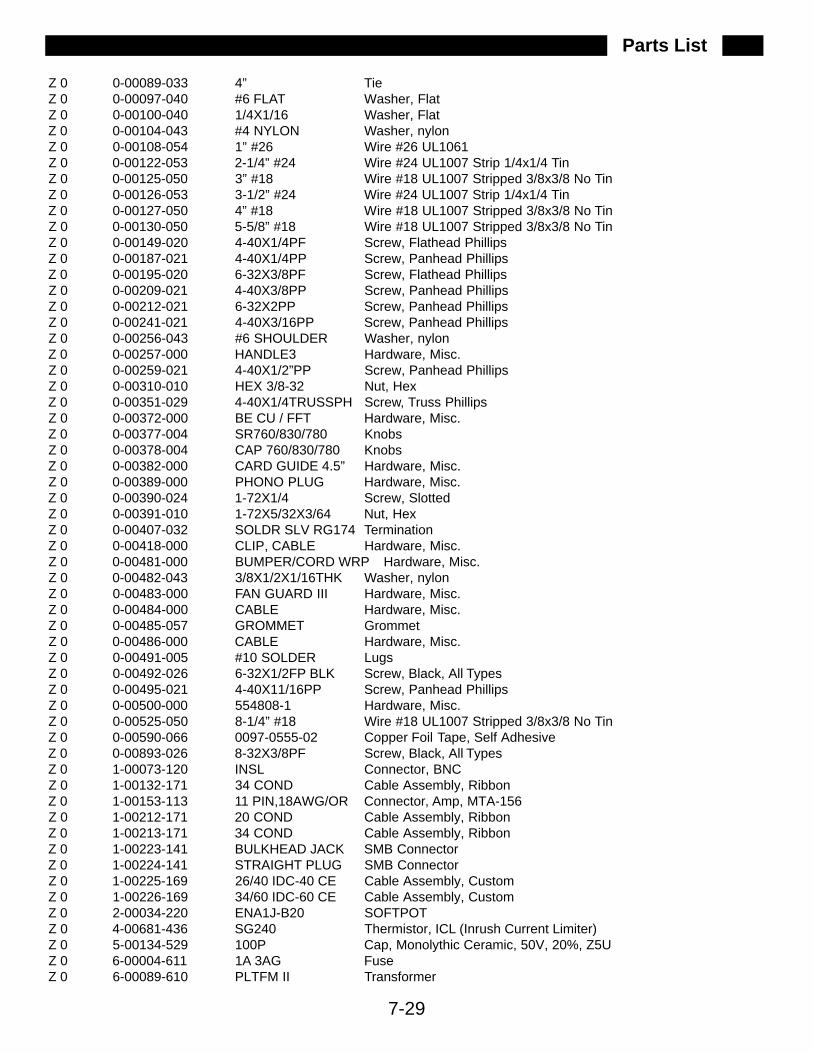
7-29
Z 0 0-00089-033 4” Tie Z 0 0-00097-040 #6 FLAT Washer, Flat Z 0 0-00100-040 1/4X1/16 Washer, Flat Z 0 0-00104-043 #4 NYLON Washer, nylon Z 0 0-00108-054 1” #26 Wire #26 UL1061 Z 0 0-00122-053 2-1/4” #24 Wire #24 UL1007 Strip 1/4x1/4 Tin Z 0 0-00125-050 3” #18 Wire #18 UL1007 Stripped 3/8x3/8 No Tin Z 0 0-00126-053 3-1/2” #24 Wire #24 UL1007 Strip 1/4x1/4 Tin Z 0 0-00127-050 4” #18 Wire #18 UL1007 Stripped 3/8x3/8 No Tin Z 0 0-00130-050 5-5/8” #18 Wire #18 UL1007 Stripped 3/8x3/8 No Tin Z 0 0-00149-020 4-40X1/4PF Screw, Flathead Phillips Z 0 0-00187-021 4-40X1/4PP Screw, Panhead Phillips Z 0 0-00195-020 6-32X3/8PF Screw, Flathead Phillips Z 0 0-00209-021 4-40X3/8PP Screw, Panhead Phillips Z 0 0-00212-021 6-32X2PP Screw, Panhead Phillips Z 0 0-00241-021 4-40X3/16PP Screw, Panhead Phillips Z 0 0-00256-043 #6 SHOULDER Washer, nylon Z 0 0-00257-000 HANDLE3 Hardware, Misc. Z 0 0-00259-021 4-40X1/2”PP Screw, Panhead Phillips Z 0 0-00310-010 HEX 3/8-32 Nut, Hex Z 0 0-00351-029 4-40X1/4TRUSSPH Screw, Truss Phillips Z 0 0-00372-000 BE CU / FFT Hardware, Misc. Z 0 0-00377-004 SR760/830/780 Knobs Z 0 0-00378-004 CAP 760/830/780 Knobs Z 0 0-00382-000 CARD GUIDE 4.5” Hardware, Misc. Z 0 0-00389-000 PHONO PLUG Hardware, Misc. Z 0 0-00390-024 1-72X1/4 Screw, Slotted Z 0 0-00391-010 1-72X5/32X3/64 Nut, Hex Z 0 0-00407-032 SOLDR SLV RG174 Termination Z 0 0-00418-000 CLIP, CABLE Hardware, Misc. Z 0 0-00481-000 BUMPER/CORD WRP Hardware, Misc. Z 0 0-00482-043 3/8X1/2X1/16THK Washer, nylon Z 0 0-00483-000 FAN GUARD III Hardware, Misc. Z 0 0-00484-000 CABLE Hardware, Misc. Z 0 0-00485-057 GROMMET Grommet Z 0 0-00486-000 CABLE Hardware, Misc. Z 0 0-00491-005 #10 SOLDER Lugs Z 0 0-00492-026 6-32X1/2FP BLK Screw, Black, All Types Z 0 0-00495-021 4-40X11/16PP Screw, Panhead Phillips Z 0 0-00500-000 554808-1 Hardware, Misc. Z 0 0-00525-050 8-1/4” #18 Wire #18 UL1007 Stripped 3/8x3/8 No Tin Z 0 0-00590-066 0097-0555-02 Copper Foil Tape, Self Adhesive Z 0 0-00893-026 8-32X3/8PF Screw, Black, All Types Z 0 1-00073-120 INSL Connector, BNC Z 0 1-00132-171 34 COND Cable Assembly, Ribbon Z 0 1-00153-113 11 PIN,18AWG/OR Connector, Amp, MTA-156 Z 0 1-00212-171 20 COND Cable Assembly, Ribbon Z 0 1-00213-171 34 COND Cable Assembly, Ribbon Z 0 1-00223-141 BULKHEAD JACK SMB Connector Z 0 1-00224-141 STRAIGHT PLUG SMB Connector Z 0 1-00225-169 26/40 IDC-40 CE Cable Assembly, Custom Z 0 1-00226-169 34/60 IDC-60 CE Cable Assembly, Custom Z 0 2-00034-220 ENA1J-B20 SOFTPOTZ 0 4-00681-436 SG240 Thermistor, ICL (Inrush Current Limiter)Z 0 5-00134-529 100P Cap, Monolythic Ceramic, 50V, 20%, Z5U Z 0 6-00004-611 1A 3AG Fuse Z 0 6-00089-610 PLTFM II Transformer
Parts List
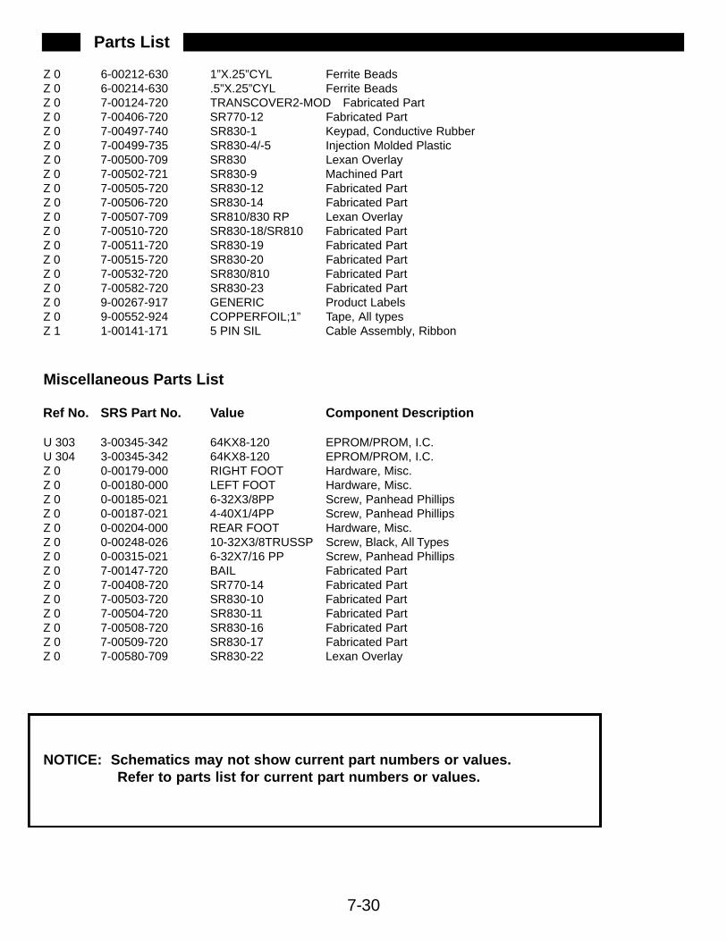
7-30
Z 0 6-00212-630 1”X.25”CYL Ferrite Beads Z 0 6-00214-630 .5”X.25”CYL Ferrite Beads Z 0 7-00124-720 TRANSCOVER2-MOD Fabricated Part Z 0 7-00406-720 SR770-12 Fabricated Part Z 0 7-00497-740 SR830-1 Keypad, Conductive Rubber Z 0 7-00499-735 SR830-4/-5 Injection Molded Plastic Z 0 7-00500-709 SR830 Lexan Overlay Z 0 7-00502-721 SR830-9 Machined Part Z 0 7-00505-720 SR830-12 Fabricated Part Z 0 7-00506-720 SR830-14 Fabricated Part Z 0 7-00507-709 SR810/830 RP Lexan Overlay Z 0 7-00510-720 SR830-18/SR810 Fabricated Part Z 0 7-00511-720 SR830-19 Fabricated Part Z 0 7-00515-720 SR830-20 Fabricated Part Z 0 7-00532-720 SR830/810 Fabricated Part Z 0 7-00582-720 SR830-23 Fabricated Part Z 0 9-00267-917 GENERIC Product Labels Z 0 9-00552-924 COPPERFOIL;1” Tape, All types Z 1 1-00141-171 5 PIN SIL Cable Assembly, Ribbon
Miscellaneous Parts List
Ref No. SRS Part No. Value Component Description
U 303 3-00345-342 64KX8-120 EPROM/PROM, I.C. U 304 3-00345-342 64KX8-120 EPROM/PROM, I.C. Z 0 0-00179-000 RIGHT FOOT Hardware, Misc. Z 0 0-00180-000 LEFT FOOT Hardware, Misc. Z 0 0-00185-021 6-32X3/8PP Screw, Panhead Phillips Z 0 0-00187-021 4-40X1/4PP Screw, Panhead Phillips Z 0 0-00204-000 REAR FOOT Hardware, Misc. Z 0 0-00248-026 10-32X3/8TRUSSP Screw, Black, All Types Z 0 0-00315-021 6-32X7/16 PP Screw, Panhead Phillips Z 0 7-00147-720 BAIL Fabricated Part Z 0 7-00408-720 SR770-14 Fabricated Part Z 0 7-00503-720 SR830-10 Fabricated Part Z 0 7-00504-720 SR830-11 Fabricated Part Z 0 7-00508-720 SR830-16 Fabricated Part Z 0 7-00509-720 SR830-17 Fabricated Part Z 0 7-00580-709 SR830-22 Lexan Overlay
NOTICE: Schematics may not show current part numbers or values. Refer to parts list for current part numbers or values.
Parts List

Parts List
7-31