
doras.dcu.iedoras.dcu.ie/17855/1/TSF.docx · Web viewSemiconductor Photonics Group, Physics...
29
Growth of n-type γ-CuCl with improved carrier concentration by pulsed dc sputtering: structural, electronic and UV emission properties K. V. Rajani 1* , F. Olabanji Lucas 2 , S. Daniels 1 , D. Danieluk 3 , A. L. Bradley 3 , A. Cowley 2 , M. M. Alam 2 and P. J. McNally 2 1 Nanomaterials Processing Laboratory, NCPST, School of Electronic Engineering, Dublin City University, Dublin 9, Ireland 2 Nanomaterials Processing Laboratory, The Rince Institute, School of Electronic Engineering, Dublin City University, Dublin 9, Ireland. 3 Semiconductor Photonics Group, Physics Department, Trinity College Dublin, Dublin 2, Ireland * Corresponding author: Tel.: +353 1 700 5872, fax: +353 1 700 5508
Transcript of doras.dcu.iedoras.dcu.ie/17855/1/TSF.docx · Web viewSemiconductor Photonics Group, Physics...
Growth of n-type γ-CuCl with improved carrier
concentration by pulsed dc sputtering: structural, electronic
and UV emission propertiesK. V. Rajani 1*, F. Olabanji Lucas 2, S. Daniels 1, D. Danieluk 3, A. L. Bradley 3, A. Cowley 2,
M. M. Alam 2 and P. J. McNally 2
1Nanomaterials Processing Laboratory, NCPST, School of Electronic Engineering, Dublin
City University, Dublin 9, Ireland
2Nanomaterials Processing Laboratory, The Rince Institute, School of Electronic
Engineering, Dublin City University, Dublin 9, Ireland.
3Semiconductor Photonics Group, Physics Department, Trinity College Dublin,
Dublin 2, Ireland
* Corresponding author: Tel.: +353 1 700 5872, fax: +353 1 700 5508
Email Address: [email protected]

Abstract
Copper (I) chloride is naturally a direct band gap, zincblende and p-type semiconductor
material with much potential in linear and non-linear optical applications owing to its large
free excitonic binding energy. In order to fabricate an efficient electrically pumped emitter, a
combination of both p-type and n-type semiconductor materials will be required. In this
study, we report on the growth of n-type γ-CuCl with improved carrier concentration by
pulsed dc magnetron sputtering of CuCl/Zn target. An improvement of carrier concentration
up to an order of ~ 9.8x1018 cm-3, which is much higher than the previously reported (~ 1016
cm-3), has been achieved. An enhancement in crystallinity of CuCl along the (111) orientation
and its consistency with the morphological studies have also been investigated as an effect of
doping. Influence of Zn wt % in the sputtering target on the Hall mobility and resistivity of
the doped films is explored. The strong ultraviolet emission of doped films is confirmed
using room temperature and low temperature photoluminescence studies.
Keywords: n-Type CuCl thin films; sputtering; Photoluminescence; Semiconductor.
1. Introduction
The investigation of materials for solid-state lighting has a fundamental role in the
development of cost-effective and environmentally friendly light sources. Wide band gap
materials like GaN and ZnO are being studied extensively by many researchers for the past
few years due to their potential applications in the fabrication of ultraviolet (UV) light
emitting diodes (LEDs) and laser diodes [1-3]. But a crucial problem associated with these
materials is the presence of threading dislocations due to the lattice mismatch with non-
parental substrates [4, 5]. Furthermore, ZnO suffers from difficulties in producing consistent
p-type material [6, 7]. The lattice mismatch between the semiconductor and the substrate can
create defect densities as high as 1010 cm-2. These defect densities tend to reduce the internal
quantum efficiencies and hence the reliability of the devices [8]. The wide band gap,
zincblende, I-VII compound semiconductor, -CuCl, could be a worthwhile candidate due to
its small lattice mismatch with Si (<0.4 %), and it has a direct band gap of approx. 3.39eV at
room temperature. Furthermore, the excitonic binding energy of CuCl is of the order of 190
meV [9], which is much higher than that of GaN (25 meV) [10], ZnO (60 meV) [11] and
other related direct band gap inorganic materials. This exciton stability could see this material
system develop into an efficient candidate for UV LEDs and diode lasers operable at room
temperature. To make use of the advantages of CuCl in real devices, there should be a
reliable technique for doping this material system.
There have been several reports on the electrical properties of cuprous chloride and
related halides by many authors: Wagner et al. [12] studied the total electrical conductivity
and hole conductivity of bulk copper halides (CuCl, CuBr and CuI) between 523 and 723 K
using AC voltages at 1 kHz and DC polarization methods; Brendahan et al. [13] investigated
the total conductivity and the electronic conductivity of CuBr thin films between 186 K and
350 K using impedance spectroscopy and DC polarization methods; Knauth et al. [14, 15]

performed room temperature Hall effect measurements and Mott-Schottky analysis on CuBr
thick films, while Lucas et al. [16, 17] probed the total conductivity and the electronic
conductivity of CuCl thin films between 160 and 400 K using impedance/admittance
spectroscopy and DC polarization methods. The summary of all these experiments is that
cuprous halides are naturally p-type mixed ionic–electronic semiconducting materials with a
very low electronic conductivity at room temperature and above. The hole conductivity arises
from a Cu deficiency δ, in the copper halide crystals (Cu1 – δ X: where X = Cl, Br or I). As part
of the effort for the realization of exciton related light emitting devices using CuCl, O’Reilly
et al. [18] co-evaporated CuCl/ZnCl2 thin films and demonstrated the first n-type CuCl based
films. However, the carrier concentration in these doped films was very low (n~ 1 ×
1016/cm3) probably due to compensation effects caused by the simultaneous introduction of
excessive Cl atoms from the co-evaporation of ZnCl2.
Here, we proceed from our previous work on the growth and characterization of CuCl
films [17-19] and move a step closer to the realization of an efficient homojunction light
emitting device based on CuCl technology by presenting the optoelectronic properties of n-
type CuCl:Zn thin films with improved carrier concentrations grown by pulsed dc magnetron
sputtering on glass and Si substrates. Unlike the vacuum evaporation technique, sputtering is
capable of depositing thin films of repeatable stoichiometry [20] which is crucial for the
reliable performance of a compound semiconductor material like CuCl:Zn. In addition to this,
the use of Zn powder instead of ZnCl2 will prevent the problems of additional Cl inclusion
during film deposition as was experienced in the co-evaporation of CuCl/ZnCl2 films [18].
2. Experimental details
Thin films of CuCl:Zn were prepared by pulsed dc magnetron sputtering of a CuCl/Zn
target, with the weight percentage of Zn in the target varying from 0-5%, onto glass and Si
substrates. Prior to deposition the substrates were ultrasonically cleaned using acetone,
trychloroethane and methanol followed by de-ionised water. An ENI RPG-100 pulse
generator was used to drive a planar magnetron fitted with the target in the power regulation
mode. The chamber was first pumped down to a base pressure of 2x10 -5 Pa by cryogenic
pumping. The target was pre-sputtered for about 10 minutes prior to deposition in order to
reduce the contamination and to obtain a stable plasma density. Sputtering was carried out in
pure argon atmosphere and the working pressure was adjusted to 0.55 Pa. The target to
substrate distance was adjusted to 6 cm. The power density at the target and duty cycle of the
pulse were optimized from a number of iterations to be 1.73 W/cm2 and 40%, respectively.
The substrates were held at floating potential and the sputtering time was adjusted to 15
minutes to obtain a uniform film thickness of 350 20 nm for all the deposited samples.
X-Ray diffraction (XRD) analysis was carried out using Copper Kα radiation of
wavelength 1.54 Ǻ from a Bruker D8 instrument to determine the crystallinity of the CuCl:Zn
films, using configuration. The morphology of the thin films was investigated using
Scanning Electron Microscopy (SEM) at an operating voltage of 13 kV. Circular gold ohmic
contacts of 1mm diameter were evaporated on the films deposited on glass substrates. Hall
effect measurements were carried out in the van der Pauw configuration using a Nanometrics
HL5500PC Hall effect system. UV/Vis absorption spectra of the films were explored using a
Perkin Elmer Lambda 40 UV/Vis spectrometer in a range of wavelengths from 320-420 nm.
Temperature dependent photoluminescence (PL) measurements were carried out from room
temperature down to 17 K by employing a closed helium cryostat system and a 355 nm
excitation laser. The photoluminescence spectra were collected on a Jobin Yvon-Horiba Triax
190 spectrometer coupled with liquid nitrogen cooled CCD detector.
3. Results and discussion
The CuCl:Zn films (samples) are deposited on glass and Si (100) substrates at room
temperature by pulsed dc magnetron sputtering of CuCl/Zn targets containing 0, 1, 3 and 5wt.
% Zn, and from here onwards these samples are designated as A, B, D and E, respectively
(See Table 1). The crystalline quality of the CuCl:Zn films was examined and the
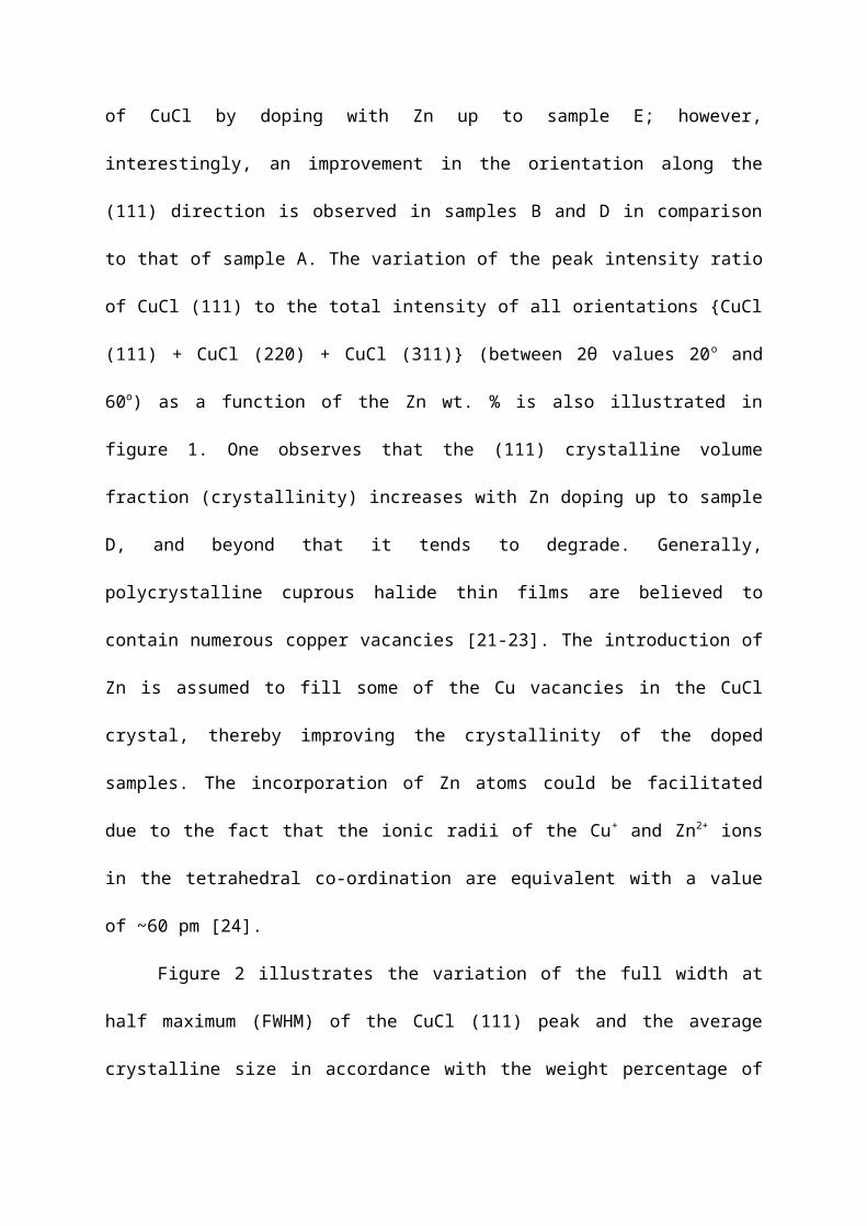
corresponding diffraction peaks were indexed. In Figure 1(inset), plots (a), (b), (c) and (d)
show the powder XRD pattern of samples A, B, D and E, respectively. All the measurements
were carried out in identical experimental conditions. The Bragg diffraction patterns of the
samples are in good agreement with the ICDD data for polycrystalline CuCl. All the samples
show the cubic zincblende structure with lattice planes oriented along (111), (220) and (311)
directions with 2θ values ~28.5, ~47.4 and ~56.3, respectively, and preferential orientation
along the (111) planes. XRD patterns indicate no sign of structural deformity of CuCl by
doping with Zn up to sample E; however, interestingly, an improvement in the orientation
along the (111) direction is observed in samples B and D in comparison to that of sample A.
The variation of the peak intensity ratio of CuCl (111) to the total intensity of all orientations
{CuCl (111) + CuCl (220) + CuCl (311)} (between 2θ values 20o and 60o) as a function of
the Zn wt. % is also illustrated in figure 1. One observes that the (111) crystalline volume
fraction (crystallinity) increases with Zn doping up to sample D, and beyond that it tends to
degrade. Generally, polycrystalline cuprous halide thin films are believed to contain
numerous copper vacancies [21-23]. The introduction of Zn is assumed to fill some of the Cu
vacancies in the CuCl crystal, thereby improving the crystallinity of the doped samples. The
incorporation of Zn atoms could be facilitated due to the fact that the ionic radii of the Cu+
and Zn2+ ions in the tetrahedral co-ordination are equivalent with a value of ~60 pm [24].
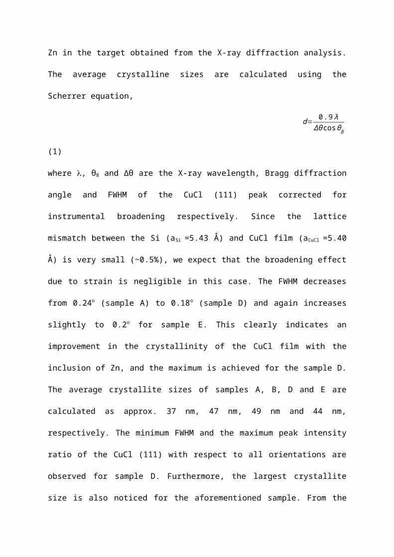
Figure 2 illustrates the variation of the full width at half maximum (FWHM) of the
CuCl (111) peak and the average crystalline size in accordance with the weight percentage of
Zn in the target obtained from the X-ray diffraction analysis. The average crystalline sizes are
calculated using the Scherrer equation,
d= 0 . 9 λ
Δθ cosθB (1)
where , θB and Δθ are the X-ray wavelength, Bragg diffraction angle and FWHM of the
CuCl (111) peak corrected for instrumental broadening respectively. Since the lattice
mismatch between the Si (aSi =5.43 Å) and CuCl film (aCuCl =5.40 Å) is very small (~0.5%),
we expect that the broadening effect due to strain is negligible in this case. The FWHM
decreases from 0.24o (sample A) to 0.18o (sample D) and again increases slightly to 0.2o for
sample E. This clearly indicates an improvement in the crystallinity of the CuCl film with the
inclusion of Zn, and the maximum is achieved for the sample D. The average crystallite sizes
of samples A, B, D and E are calculated as approx. 37 nm, 47 nm, 49 nm and 44 nm,
respectively. The minimum FWHM and the maximum peak intensity ratio of the CuCl (111)
with respect to all orientations are observed for sample D. Furthermore, the largest crystallite
size is also noticed for the aforementioned sample. From the XRD results, one observes that
the doping of CuCl films with 3 wt. % Zn (sample D) appears to be the optimum process and
further increases in target Zn concentrations result in a reduction in the (111) crystalline
volume fraction and crystalline size (sample E). The reduction in the crystal properties may
be due to the segregation of dopants in the grain boundaries beyond a doping level
corresponding to sample D (> 3 wt. % Zn in the target). This hypothesis is examined using
SEM analysis of the appearance of non-uniform grains with irregular orientations.
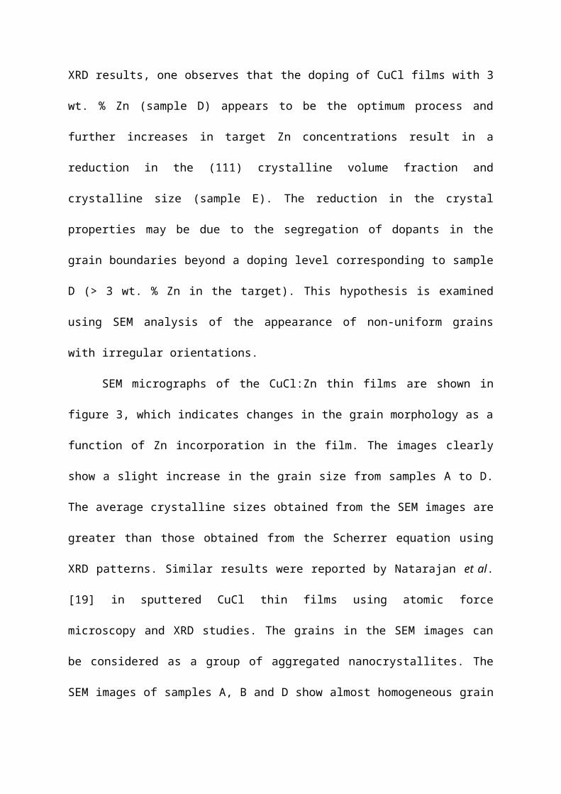
SEM micrographs of the CuCl:Zn thin films are shown in figure 3, which indicates
changes in the grain morphology as a function of Zn incorporation in the film. The images
clearly show a slight increase in the grain size from samples A to D. The average crystalline
sizes obtained from the SEM images are greater than those obtained from the Scherrer
equation using XRD patterns. Similar results were reported by Natarajan et al. [19] in
sputtered CuCl thin films using atomic force microscopy and XRD studies. The grains in the
SEM images can be considered as a group of aggregated nanocrystallites. The SEM images
of samples A, B and D show almost homogeneous grain morphology, with uniform
orientation of grains, while that of the sample E shows grains with irregular size and shape
with different orientations. This is confirmed by the XRD pattern via a decrease in the peak
intensity ratio of the CuCl (111) peak to total intensity of all orientations as shown in figure
1.
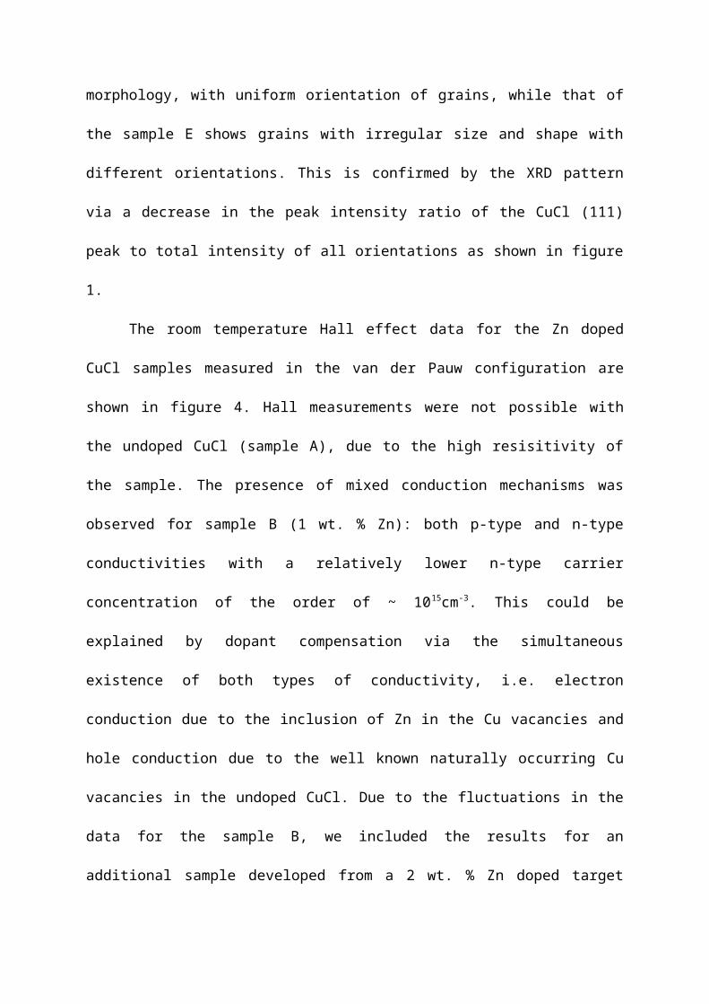
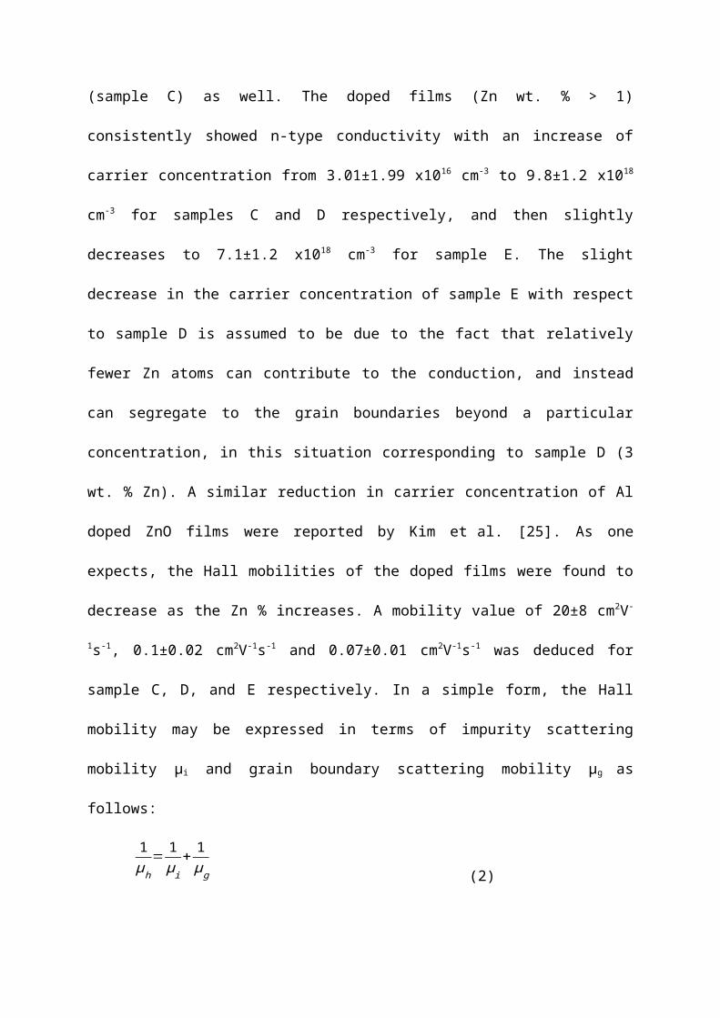
The room temperature Hall effect data for the Zn doped CuCl samples measured in
the van der Pauw configuration are shown in figure 4. Hall measurements were not possible
with the undoped CuCl (sample A), due to the high resisitivity of the sample. The presence of
mixed conduction mechanisms was observed for sample B (1 wt. % Zn): both p-type and n-
type conductivities with a relatively lower n-type carrier concentration of the order of ~
1015cm-3. This could be explained by dopant compensation via the simultaneous existence of
both types of conductivity, i.e. electron conduction due to the inclusion of Zn in the Cu
vacancies and hole conduction due to the well known naturally occurring Cu vacancies in the
undoped CuCl. Due to the fluctuations in the data for the sample B, we included the results
for an additional sample developed from a 2 wt. % Zn doped target (sample C) as well. The
doped films (Zn wt. % > 1) consistently showed n-type conductivity with an increase of
carrier concentration from 3.01±1.99 x1016 cm-3 to 9.8±1.2 x1018 cm-3 for samples C and D
respectively, and then slightly decreases to 7.1±1.2 x1018 cm-3 for sample E. The slight
decrease in the carrier concentration of sample E with respect to sample D is assumed to be
due to the fact that relatively fewer Zn atoms can contribute to the conduction, and instead
can segregate to the grain boundaries beyond a particular concentration, in this situation
corresponding to sample D (3 wt. % Zn). A similar reduction in carrier concentration of Al
doped ZnO films were reported by Kim et al. [25]. As one expects, the Hall mobilities of the
doped films were found to decrease as the Zn % increases. A mobility value of 20±8 cm 2V-1s-
1, 0.1±0.02 cm2V-1s-1 and 0.07±0.01 cm2V-1s-1 was deduced for sample C, D, and E
respectively. In a simple form, the Hall mobility may be expressed in terms of impurity
scattering mobility µi and grain boundary scattering mobility µg as follows:
1μh
= 1μi
+ 1μg (2)
The sharp decrease in the mobility from sample C (2 wt. %Zn) to D (3 wt. % Zn) can
be attributed mainly to the impact of increased impurity scattering. The presence of grain
boundaries and trapped interface charges in semiconductors results in inter-grain band
bending and potential barriers which are well known to cause a considerable reduction in the
resultant Hall mobility [26]. A further reduction in the mobility of sample E in comparison to
sample D may be ascribed to be the combination of both impurity scattering and grain
boundary scattering mechanisms as the presence of more grain boundaries was observed in
the SEM image of sample E (see figure 3).
The variation of resistivities of the samples is also illustrated in figure 4 (inset). A
value of 250 Ω cm was previously reported as the room temperature resistivity for undoped
CuCl films using 4 point probe measurement [18]. The resistivities of the samples decrease to
a minimum value of ~ 6 Ω cm for the sample D, and increase to ~ 11 Ω cm for sample E.
Obviously, the reduction of resistivity of sample D is due to higher carrier concentration
while the slight increase in resistivity of the sample E is due to a slight reduction in carrier
concentration perhaps combined with the effect of increased grain boundary scattering as
explained earlier. The electrical measurements confirm the efficacy of pulsed dc magnetron
sputtering as a means of incorporating Zn in to the CuCl crystal lattice. The substitutional Zn
leads to optimal carrier concentrations and resistivities for 3 wt. % Zn in the CuCl/Zn sputter
target. We are currently looking at means of improving the mobility of these doped samples
via post deposition thermal treatments. In addition X-ray fine structure experiments are
planned in order to confirm the substitutional site for Zn, i.e. ZnCu.
The room temperature UV-Vis absorption spectra for the CuCl:Zn films is shown in
figure 5. Herein, the major peaks correspond to both high and low energy excitonic bands
known as the Z1, 2 and Z3 excitons, respectively. The Z1, 2 and Z3 excitons are due to the
coupling of the lowest conduction band state Г6 to both the uppermost valence band holes, Г8
(Z1,2) and Г7 (Z3), respectively [9, 27]. The Z1,2 peak at ~ 372 nm (3.34eV) and the shoulder Z3
peak at ~ 379 nm (3.28eV) are in good agreement with the previously reported absorption
data for the undoped CuCl [18].
The PL measurements for all the samples (both doped and undoped) showed similar
excitonic emissions at all temperatures. Figure 6 shows the temperature dependence of the PL
spectrum of sample D. This graph clearly delineates four main peaks represented as Z3
(~3.21eV), I1 (~3.19eV), M (~3.17eV) and N1 (~3.14eV), corresponding to the Z3 free exciton,
I1 impurity bound exciton, M free biexciton and N1 impurity bound exciton, respectively. The
impurity corresponding to the I1 peak has already been reported as being due to a copper
vacancy [28], the M free biexciton results from exciton-exciton collisions [9] and the N1 peak
originates from a biexciton bound to an impurity. These results are in agreement with the
previously reported low temperature PL data of the undoped CuCl [17, 18], indicating that
the optical properties of the doped films are not compromised as a result of incorporation of
Zn atoms. As the temperature increases, the rate of decrease of the peak intensities of I 1 and
N1 become higher compared to that of the Z3 free excitonic peak intensity, and the spectra
become dominated by the Z3 peak above 100 K up to room temperature due to the high free
excitonic binding energy of CuCl. The influence of temperature on the Z3 free exciton peak is
manifested as a peak energy shift from ~3.205 eV to ~3.248 eV for a temperature increase
from 17 K to room temperature. The increase in the energy value of the Z3 free exciton as the
temperature increases corresponds to an increase in the band gap energy and was
theoretically and experimentally analysed for undoped CuCl samples by Garro et al. [29].
Analogous results in thin films and nanocrystals of CuCl have been reported previously [30,
31].
4. Conclusion
A reliable method for the development of n-type CuCl with improved carrier
concentration using pulsed dc magnetron sputtering has been presented in this study. The
resistivity of the Zn doped CuCl film was found to decrease by more than an order of
magnitude compared to the undoped CuCl film with an average maximum carrier
concentration of ~ 9.8x1018 cm-3 and a minimum average resistivity of ~ 6 cm for 3 wt. %
Zn doped samples. Improvement in the crystallinity of CuCl films by doping with Zn has
been investigated, and maximum crystallinity is obtained for 3 wt. % Zn doped sample. The
strong UV emission of the doped films confirms its utility in the optoelectronic field.
Acknowledgements
This project was funded by the Science Foundation Ireland Research Frontiers
Programme (Project#06/RFP/ENE/027) and by the Enterprise Ireland
Commercialisation Fund for Technology Development (Project#
CFTD/07/IT/331). This work was part-funded by the Irish Higher Education Authority
PRTLI "INSPIRE" project. The authors would like to thank Mr. Billy Roarty for his technical
support.
References
[1] S. Nakamura, T. Mukai, T. Senoh, Appl. Phys. Lett. 64 (1994) 1687.
[2] Y. Ryu, T.S. Lee, J.A. Lubguban, H.W. White, B.J. Kim, Y.S. Park, C.J. Youn,
Appl. Phys. Lett. 88 (2006) 241108.
[3] D.M. Bagnall, Y.F. Chen, Z. Zhu, T. Yao, S. Koyama, M.Y. Shen, T. Goto,
Appl. Phys. Lett. 70 (1997) 2230.
[4] J.K. Jeong, J.H. Choi, H.J. Kim, H.C. Seo, H.J. Kim, E. Yoon, C.S. Hwang, H.J.
Kim, J. Cryst. Growth 276 (2005) 407.
[5] X. Li, S.G. Bishop, J.J. Coleman, Appl. Phys. Lett. 73 (1998) 1179.
[6] T.M. Barnes, K. Olson, C.A. Wolden, Appl.Phys.Lett. 86 (2005) 112112.
[7] K. Minegishi, Y. Koiwai, Y. Kikuchi, K. Yano, M. Kasuga, A. Shimizu, Jpn. J. Appl.
Phys. 36 (1997) L1453.
[8] A. Bergh, G. Craford, A. Duggal, R. Haitz, Phys. Today 54 (2001) 42.
[9] M. Nakayama, H. Ichida, H. Nishimura, J. phys.: Condens. Matter 11(1999) 7653.
[10] B. Monemar, Phys. Rev. B. 10 (1974) 676.
[11] Y.R. Ryu, T.S. Lee, H.W. White, Appl. Phys. Lett. 83 (2003) 87.
[12] J.B. Wagner, C.Wagner, J. Chem. Phys. 26 (1957) 1597.
[13] M. Bendahan, C. Jacolin, P. Lauque, J.L. Seguin, P. Knauth, J. Phys. Chem. B 105
(2001) 8327.
[14] P. Knauth, Y. Massiani, J. Electroanal. Chem. 442 (1998) 229.
[15] P. Knauth, Y. Massiani, P. Pasquinelli, Phys. Stat. Sol. 165 (1998) 461.
[16] F.O. Lucas, P.J. McNally, S. Daniels, D.M. Taylor, J. Mater. Sci: Mater. Electron.
20 (2009) S144.
[17] F.O. Lucas, A. Mitra, P.J. McNally, S. Daniels, A.L. Bradley, D.M. Taylor, Y.Y.
Proskuryakov, K. Durose, D.C. Cameron, J. Phys. D: Appl. Phys. 40 (2007) 3461.
[18] L.O’Reilly, A. Mitra, G. Natarajan, O.F. Lucas, P.J. McNally, S. Daniels,
D.C. Camron, A.L. Bradley, A. Reader, J. Cryst. Growth 287 (2006) 139.
[19] Gomathi Natarajan, S. Daniels, D.C. Cameron, L.O’Reilly, A. Mitra, P.J. McNally,
O.F. Lucas, R.T. Rajendra Kumar, I. Reid, A.L. Bradley, J. Appl. Phys.100
(2006) 033520.
[20] R. Schmidt, A. Basu, A.W. Brinkman, J. Eur. Ceram. Soc. 24 (2004) 1233.
[21] S. Kondo, K. Mikami, T. Saito, Opt. Mater. 30 (2008) 473.
[22] R.S. Bradley, D.C. Munro, P.N. Spencer, Trans. Faraday. Soc. 65 (1969) 1912.
[23] M. Ueta, H. Kazaki, K. Kobayashi, Y.Toyozawa, E. Hanamura, Excitonic
Processes in solid (Springer : Berlin. 1986).
[24] R. D. Shannon, Acta Crystallogr. A 32 (1976) 751.
[25] K.H. Kim, K.C. Park, D. Y. Ma, J. Appl. Phys. 81(1997) 7764.
[26] T. Pisarkiewicz, K. Zakrzewska, E. Leja, Thin Solid Films 174 (1989) 217.
[27] A. Goldmann, Phys.Stat. Sol (b). 81 (1977) 9.
[28] M. Certier, C.Wecker, S. Nikitine, J. Phys. Chem. Solids 30 (1969) 2135.
[29] N. Garro, A. Cantarero, M. Cardona, T. Ruf, A. Gobel, C. Lin, K. Reimann, K.
Rtibenacke, M. Steube, Solid State Commun. 98 (1996) 27.
[30] A.Gobel, T. Ruf, M. Cardona, C.T. Lin, J. Wrzesinski, M. Steube, K. Reimann, J.C.
Merle, M. Joucla, Phys. Rev. B. 57 (1998) 15183.
[31] O. Pages, H. Erguig, A. Lazreg, A. Katty, A. Lusson, O. Gorochov, Mater. Sci. Eng. B
69 (2000) 431.
List of figure captions:
Figure 1. Variation of (111) peak intensity to the total intensity of all orientations as a
function of the Zn wt. % in the target. The inset graph shows the X-Ray powder diffraction
pattern for samples corresponding to (a) 0 wt. %, (b) 1 wt. %, (c) 5 wt. % and (d) 3 wt. % Zn
doped CuCl targets.
Figure 2. Variation of FWHM of CuCl (111) peak and average crystal size of the CuCl: Zn
film as a function of the weight percentage of Zn in the target.
Figure 3. SEM micrographs of CuCl: Zn films with (a) 0 wt. %, (b) 1 wt. %, (c) 3 wt. %, and
(d) 5 wt. % Zn in the target.
Figure 4. Variation of resistivity, carrier concentration and mobility (inset) as a function of
the wt. % of Zn in the target. Sample notation is indicated in Table 1.
Figure 5. Room temperature UV-Vis absorption of (a) 3 wt. % Zn doped CuCl and (b)
undoped CuCl.
Figure 6. Temperature dependence and room temperature PL spectrum (inset) of 3 wt. % Zn
doped CuCl films.
0 1 2 3 4 50.75
0.80
0.85
0.90
0.95
1.00
1.05
Peak
inte
nsity
ratio
of (
111)
to a
ll orie
ntat
ions
Zn Wt. % in target
20 30 40 50 60
CuCl
(311
)
CuCl
(220
)
dc b aIn
tens
ity (a
rb.u
nits)
2theta (deg)
CuCl
(111
)
Table 1
Sample notation used in the text.
Figure 1
SampleWt % of Zn in
the targetABCDE
01235
0 1 2 3 4 50.18
0.19
0.20
0.21
0.22
0.23
0.24
0.25
Crys
tal s
ize (n
m)
FWHM
(deg
)
Wt. % of Zn in the target
36
38
40
42
44
46
48
50
Figure 2
Figure 3
1 2 3 4 5 6
101
102
103
Carrier concentration Resistivity Mobility
Carri
er co
ncen
tratio
n (cm-3
)
Resis
tivity
( cm
)
Zn wt.% in target
1014
1015
1016
1017
1018
1019
0 1 2 3 4 510-1
100
101
102
Mob
ility (
cm2 /V
s)
Zn wt.% in target
320 340 360 380 400 420
(b)
(a)
Z3
Z12
Abso
rban
ce (a
rb.u
nits)
Wavelength (nm)
Figure 4
Figure 5
370 380 390 400 410 420
N1
MI1
Z3 17 K30 K50 K80 K
100 K
Inte
nsity
(arb
.unit
s)
Wavelength (nm)
360 370 380 390 400
Inte
nsity
(arb
.unit
s)
Wavelength (nm)
Figure 6