Doc.Number SOP,Heidelberg μPG 501...
14
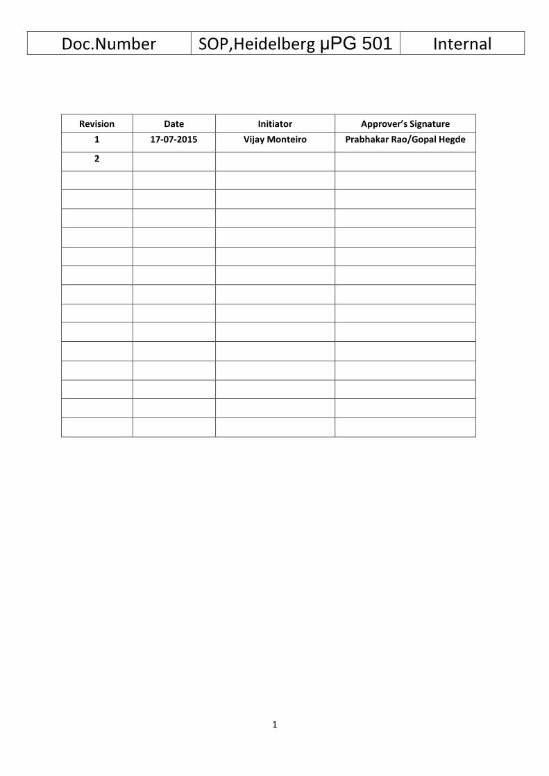
Doc.Number SOP,Heidelberg μPG 501 Internal 1 Revision Date Initiator Approver’s Signature 1 17-07-2015 Vijay Monteiro Prabhakar Rao/Gopal Hegde 2
Transcript of Doc.Number SOP,Heidelberg μPG 501...
Doc.Number SOP,Heidelberg μPG 501 Internal
1
Revision Date Initiator Approver’s Signature
1 17-07-2015 Vijay Monteiro Prabhakar Rao/Gopal Hegde
2
Doc.Number SOP,Heidelberg μPG 501 Internal
2
1. Purpose
This document describes the steps to be followed by the user, to perform
direct writing /mask writing on the substrate/Mask.
2. Scope
It covers the instructions for operation the system, the safety precautions to
be followed while operating the system and the penalty, in case of any
deviations from following SOP.
3. Pre-Checks on Tool
a. Ensure that all the details have been entered into the FOM system. b. Ensure that the Power is switched “ON” for both the tool and computer.
Doc.Number SOP,Heidelberg μPG 501 Internal
3
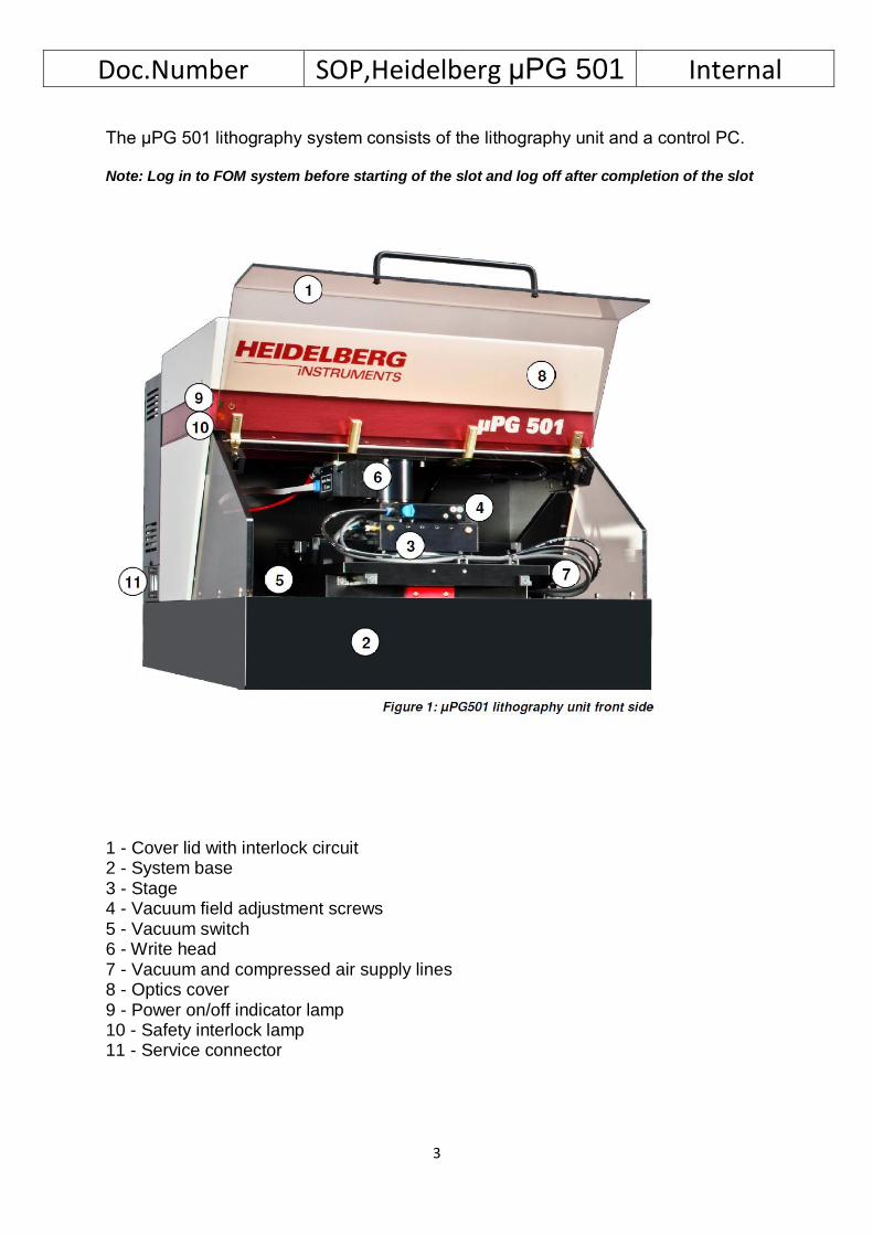
The μPG 501 lithography system consists of the lithography unit and a control PC. Note: Log in to FOM system before starting of the slot and log off after completion of the slot
1 - Cover lid with interlock circuit 2 - System base 3 - Stage 4 - Vacuum field adjustment screws 5 - Vacuum switch 6 - Write head 7 - Vacuum and compressed air supply lines 8 - Optics cover 9 - Power on/off indicator lamp 10 - Safety interlock lamp 11 - Service connector
Doc.Number SOP,Heidelberg μPG 501 Internal
4
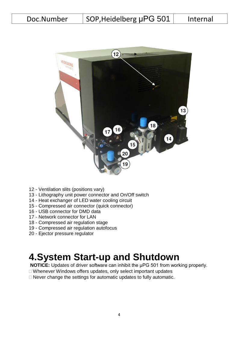
12 - Ventilation slits (positions vary) 13 - Lithography unit power connector and On/Off switch 14 - Heat exchanger of LED water cooling circuit 15 - Compressed air connector (quick connector) 16 - USB connector for DMD data 17 - Network connector for LAN 18 - Compressed air regulation stage 19 - Compressed air regulation autofocus 20 - Ejector pressure regulator
4.System Start-up and Shutdown NOTICE: Updates of driver software can inhibit the μPG 501 from working properly.
Whenever Windows offers updates, only select important updates
Never change the settings for automatic updates to fully automatic.
Doc.Number SOP,Heidelberg μPG 501 Internal
5
STARTUP 1. At the Lithography Unit, switch on the μPG 501 with the On/Off switch (13). The Power On/Off Indicator Lamp (9) lights up. 2. Make sure that air pressure for the stage is applied and the lid is closed. The Safety Interlock Lamp (10) should be off. 3. Power up the Menu PC according to the manufacturer’s instructions. Factory settings for login are user upg501, password upg501. 4. Start the Exposure Wizard. When starting the wizard after a shutdown, startup takes approximately a minute due to the necessary initialization processes. 5. With the wizard, the camera software HI Vision starts. Do not close the camera window while the wizard is running, otherwise the wizard may crash and has to
be restarted. 6. Once the startup sequence of the wizard is finished, run a stage initialization (Tools Initialize Stage)
SHUTDOWN
1. Close the wizard (FileExit). It takes around 10 seconds for the software to finish all background processes before the wizard itself stops. 2. Switch off the μPG system with the On/Off switch (13). The Power On/Off Indicator Lamp (9) goes out. 3. Power down the Menu PC according to the manufacturer's instructions.
RESTART 1. Close the wizard (File Exit). 2. Switch off the μPG system with the On/Off switch (13). 3. Wait ~20 seconds. 4. Switch on the μPG system. 5. If required (e.g., because of communication problems), reboot the User PC according to the manufacturer's instructions. Factory settings for login are user upg501, password upg501. 6. Start the Exposure Wizard. 7. With the wizard, the camera software HI Vision starts. Do not close the camera window while the wizard is running, otherwise the wizard may crash and has to
be restarted. 8. Once the startup sequence of the wizard is finished, run a stage initialization (ToolsInitialize Stage)
Design Data GDS-2 or CIF is the preferred format of the design.
Doc.Number SOP,Heidelberg μPG 501 Internal
6
5.CHOICE OF SUBSTRATE To do lithographic exposures, substrates and especially the photosensitive coating of the substrates have to be chosen according to the intended application. In addition, the specifications have to fall into the specification range of the μPG 501. Standard substrates:
for mask making to use e.g., in a stepper:
o soda-lime or quartz plates (depending on the requirements concerning
temperature stability) o size between 2” and 5”
o maximum thickness 6mm
o flatness < ± 20μm
o chromium coating with anti-reflection layer (e.g., chromium-oxide)
for direct writing on wafers: o silicon wafers (for other wafer types, please contact the Heidelberg Instruments
Customer Support on information if they are usable at all, and recommendations on exposure and processing)
o size between 2” and 5”
o maximum thickness 6mm
o flatness < ± 20μm
Recommended photoresist coatings: AZ5214E, AZ1518, S1813, S1805 General Advice:
Take care to protect the substrates from light (even safe light, as far as possible) and humidity at all times until developing is finished.
Always wear lint-free gloves (e.g. Latex) when handling the substrates.
Protect the substrate from scratches whenever transporting it. Use only designated transport boxes.
Never use out-of-date batches.
Carefully clean the back side of the substrate before use to make sure it gets good vacuum suction on the μPG 501 stage chuck.
Don’t expose substrates to water, humidity, solvents, or solvent fumes.
6.EXPOSURE PROCEDURE For easy use, the μPG 501 provides an Exposure Wizard that guides the operator through the steps of an exposure. There are three different types of exposure: the standard exposure, an exposure with alignment to existing structures, and the optional target mode exposure that allows to directly expose structures defined in the camera image.
Doc.Number SOP,Heidelberg μPG 501 Internal
7
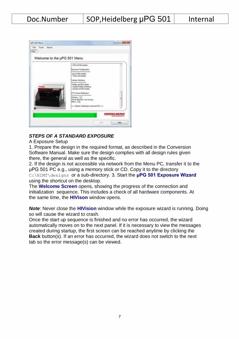
STEPS OF A STANDARD EXPOSURE A Exposure Setup 1. Prepare the design in the required format, as described in the Conversion Software Manual. Make sure the design complies with all design rules given there, the general as well as the specific. 2. If the design is not accessible via network from the Menu PC, transfer it to the μPG 501 PC e.g., using a memory stick or CD. Copy it to the directory C:\HIMT\designs or a sub-directory. 3. Start the μPG 501 Exposure Wizard
using the shortcut on the desktop. The Welcome Screen opens, showing the progress of the connection and initialization sequence. This includes a check of all hardware components. At the same time, the HIVison window opens. Note: Never close the HIVision window while the exposure wizard is running. Doing
so will cause the wizard to crash. Once the start up sequence is finished and no error has occurred, the wizard automatically moves on to the next panel. If it is necessary to view the messages created during startup, the first screen can be reached anytime by clicking the Back button(s). If an error has occurred, the wizard does not switch to the next tab so the error message(s) can be viewed.
Doc.Number SOP,Heidelberg μPG 501 Internal
8
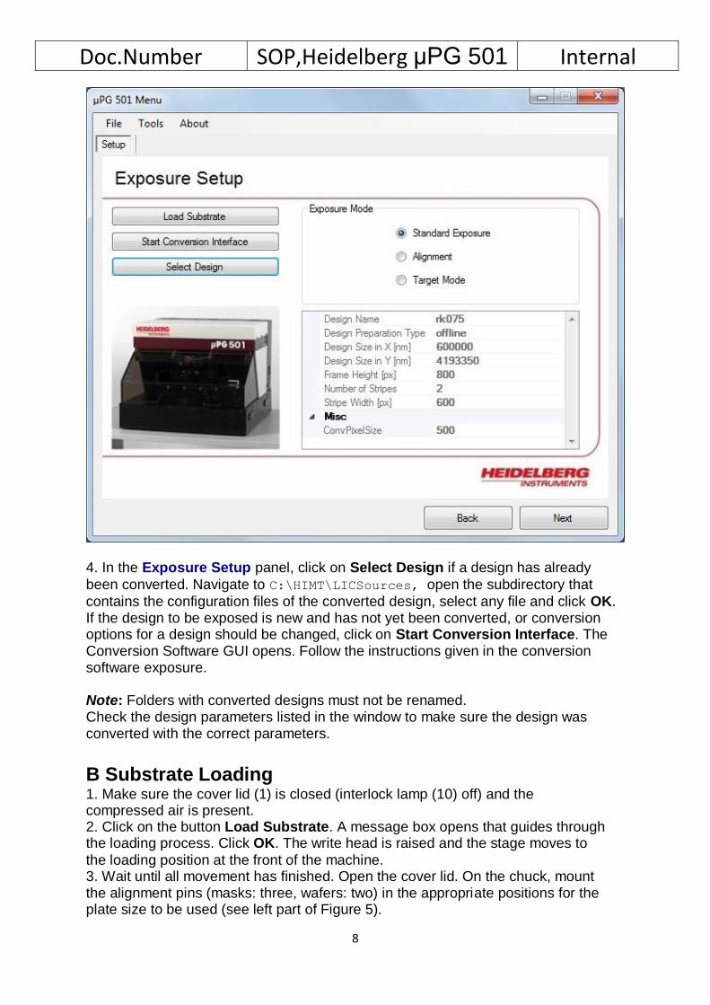
4. In the Exposure Setup panel, click on Select Design if a design has already
been converted. Navigate to C:\HIMT\LICSources, open the subdirectory that
contains the configuration files of the converted design, select any file and click OK. If the design to be exposed is new and has not yet been converted, or conversion options for a design should be changed, click on Start Conversion Interface. The Conversion Software GUI opens. Follow the instructions given in the conversion software exposure. Note: Folders with converted designs must not be renamed. Check the design parameters listed in the window to make sure the design was converted with the correct parameters.
B Substrate Loading 1. Make sure the cover lid (1) is closed (interlock lamp (10) off) and the compressed air is present. 2. Click on the button Load Substrate. A message box opens that guides through the loading process. Click OK. The write head is raised and the stage moves to
the loading position at the front of the machine. 3. Wait until all movement has finished. Open the cover lid. On the chuck, mount the alignment pins (masks: three, wafers: two) in the appropriate positions for the plate size to be used (see left part of Figure 5).
Doc.Number SOP,Heidelberg μPG 501 Internal
9
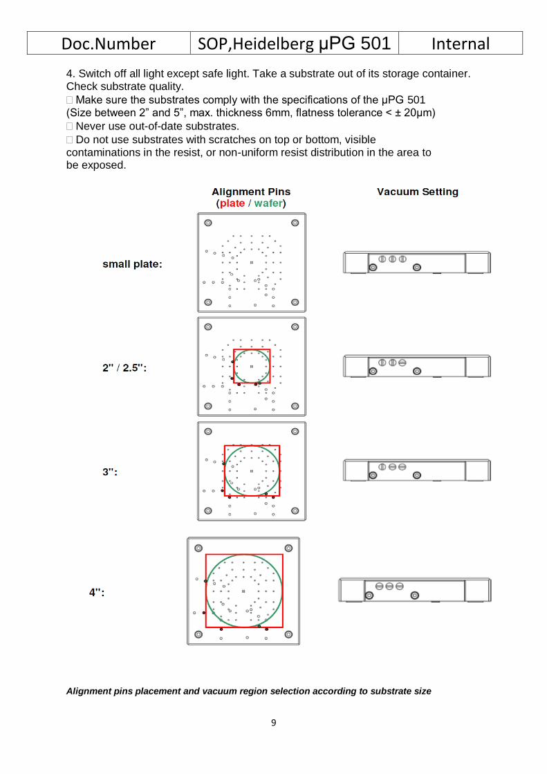
4. Switch off all light except safe light. Take a substrate out of its storage container. Check substrate quality.
Make sure the substrates comply with the specifications of the μPG 501 (Size between 2” and 5”, max. thickness 6mm, flatness tolerance < ± 20μm)
Never use out-of-date substrates.
Do not use substrates with scratches on top or bottom, visible contaminations in the resist, or non-uniform resist distribution in the area to be exposed.
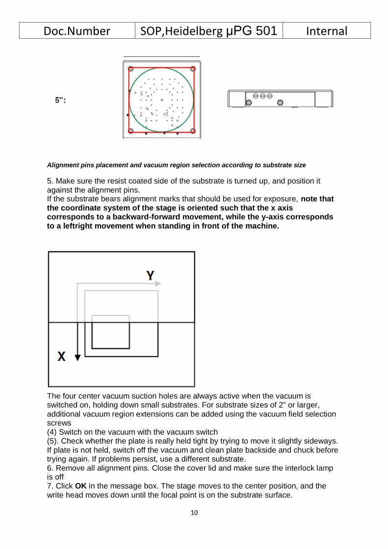
Alignment pins placement and vacuum region selection according to substrate size
Doc.Number SOP,Heidelberg μPG 501 Internal
10
Alignment pins placement and vacuum region selection according to substrate size
5. Make sure the resist coated side of the substrate is turned up, and position it against the alignment pins. If the substrate bears alignment marks that should be used for exposure, note that the coordinate system of the stage is oriented such that the x axis corresponds to a backward-forward movement, while the y-axis corresponds to a leftright movement when standing in front of the machine.
The four center vacuum suction holes are always active when the vacuum is switched on, holding down small substrates. For substrate sizes of 2" or larger, additional vacuum region extensions can be added using the vacuum field selection screws (4) Switch on the vacuum with the vacuum switch (5). Check whether the plate is really held tight by trying to move it slightly sideways. If plate is not held, switch off the vacuum and clean plate backside and chuck before trying again. If problems persist, use a different substrate. 6. Remove all alignment pins. Close the cover lid and make sure the interlock lamp is off 7. Click OK in the message box. The stage moves to the center position, and the write head moves down until the focal point is on the substrate surface.
Doc.Number SOP,Heidelberg μPG 501 Internal
11
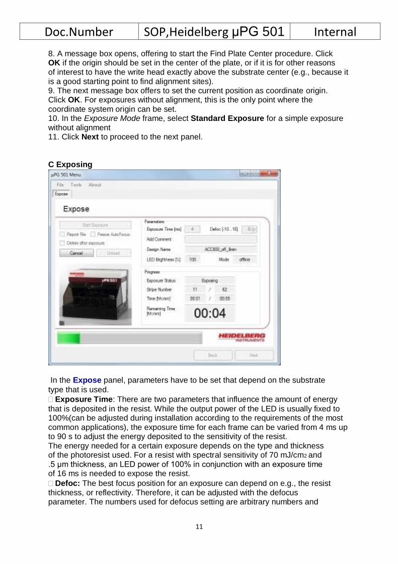
8. A message box opens, offering to start the Find Plate Center procedure. Click OK if the origin should be set in the center of the plate, or if it is for other reasons of interest to have the write head exactly above the substrate center (e.g., because it is a good starting point to find alignment sites). 9. The next message box offers to set the current position as coordinate origin. Click OK. For exposures without alignment, this is the only point where the coordinate system origin can be set. 10. In the Exposure Mode frame, select Standard Exposure for a simple exposure without alignment 11. Click Next to proceed to the next panel. C Exposing
In the Expose panel, parameters have to be set that depend on the substrate
type that is used.
Exposure Time: There are two parameters that influence the amount of energy
that is deposited in the resist. While the output power of the LED is usually fixed to 100%(can be adjusted during installation according to the requirements of the most common applications), the exposure time for each frame can be varied from 4 ms up to 90 s to adjust the energy deposited to the sensitivity of the resist. The energy needed for a certain exposure depends on the type and thickness of the photoresist used. For a resist with spectral sensitivity of 70 mJ/cm2 and .5 μm thickness, an LED power of 100% in conjunction with an exposure time of 16 ms is needed to expose the resist.
Defoc: The best focus position for an exposure can depend on e.g., the resist thickness, or reflectivity. Therefore, it can be adjusted with the defocus parameter. The numbers used for defocus setting are arbitrary numbers and
Doc.Number SOP,Heidelberg μPG 501 Internal
12
range from –10…10. The full range corresponds roughly to the focal depth of the exposure lens (~ 10 μm). NOTICE: Manual focusing while this function is active can lead to irreversible
damage to the system. Don’t use any focusing functions before the freezing is deactivated. Check again if air pressure is OK, the lid is closed, and no alignment pins have been left in the stage chuck. Click Start Exposure.
During an exposure, the exposure status is shown online in the window. Make sure that during the complete exposure time the cover lid stays closed, and no white light is switched on in the room. In addition, to get best results, avoid vibrations caused by people passing by or by heavy loads being moved on the floor close to the system. To interrupt an exposure, click on Cancel and confirm.
D Unloading 1. After exposure is finished, if no further designs should be exposed on the same plate, click on Unload.
2. Wait until all movement has stopped. 3. Open the lid, switch off the vacuum with the vacuum switch and carefully lift the substrate off the chuck. Store it in a light-proof transport box. 4. Process the substrate as soon as possible according to the substrate type and manufacturers recommendation. 5. For further exposures of the same design on the same substrate, adjust parameters if required and restart. For a different exposure on the same substrate, use the Back button to get back to the Exposure Setup panel.
SUBSTRATE PROCESSING The steps of processing of a substrate are:
Post exposure bake: Depending on application and resist type, a post exposure bake of the exposed substrate on a hot plate or in an oven may be required. Refer to the resist manufacturer’s documentation for specific information on this. The resists recommended here for standard purposes do not need a post exposure bake.
Developing: The exposed parts of the resist have been chemically altered by the light and can now be washed out of the resist layer by use of specific developer chemicals. If the energy dose was sufficient to enable the reaction through the complete layer, after developing, the surface of the coated substrate is accessible wherever the resist was exposed with full intensity. In regions where the energy dose was below the limit, only a part of the layer is removed, thus allowing for three dimensional structuring of sufficiently thick resist layers. Note: In negative resist such as SU8, the developer removes the parts which were not exposed. Developing times depend on resist type, resist thickness, and developer type, as well as the energy dose used during exposure. Typical developing times are 1 – 1.5 minutes for thin resists, and around 0.5 minutes/μm for thick resists. The combination of energy and developing technique can influence the quality of an exposure result strongly. Using too high energy during exposure or using too
Doc.Number SOP,Heidelberg μPG 501 Internal
13
strong developer makes the developing time very critical, leading to plate-toplate structure size variations. On the other hand, too low energy or too diluted developer can lead to angled and irregular resist walls, causing bad linewidth stability and rough pattern edges. The best combination of exposure parameters and processing procedure for a specific application has to be found by series of test exposures.
Hard bake: A hard bake can serve to better prepare the remaining resist layer for
the next processing step by hardening it. On the down side, it can round sharp resist edges and lead to rifts in the resist layer. Again, it depends on application and resist if a hard bake is required and recommendable, and how it should be used. Material recommendations:
developer: TMAH series (metal-ion free), or 351B.
rinsing: all rinsing during processing should be done with DI water
stripper: commercial stripper, or concentrated NaOH solution (e.g., undiluted developer) after exposure of the remaining resist with an UV lamp
cleaning: after the processing, chrome plates can be cleaned with solvents and piranha clean. Standard Process for mask writing
1. Soda lime mask (530nm AZ1518 Resist,110nm Chrome deposition) Exposure setting: For minimum feature 1 micron – Dose 28, Defocus -2 Above 3um : Dose 22 , Defocus -2 Developer AZ351B (1:4) for 1 Min, Chrome etch – 45 secs and Piranha clean of the mask
General advice:
Never use out-of-date chemicals.
If a dilution is used as developer, always shake well before use so the heavier parts are well distributed.
Take care that all materials and tools involved in processing – wipes, trays, sinks, taps, pincers etc. – are always clean.
Take care that chemicals are not mixed. Alwayse rinse well the substrate and any containers used before proceeding to the next step.
For dilutions, only use DI water.
Take care that no air bubbles stay on the substrate when submerging it into a chemical. This is especially critical during etching, where air might be caught in small structures or round holes in the resist, preventing them from being etched into the layer beneath.

Doc.Number SOP,Heidelberg μPG 501 Internal
14
NOTE: Any deviations from this SOP will be
considered as a breach of User Agreement conditions
and will result in appropriate disciplinary action.