DMOS dual full bridge driver - tme.eu€¦ · 5/23 L6206 PACKAGE Name Type Function SO24/...
23
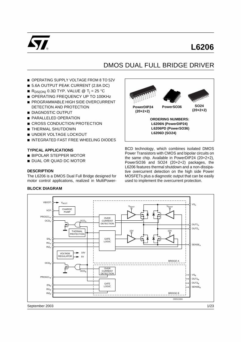
1/23 L6206 September 2003 ■ OPERATING SUPPLY VOLTAGE FROM 8 TO 52V ■ 5.6A OUTPUT PEAK CURRENT (2.8A DC) ■ R DS(ON) 0.3Ω TYP. VALUE @ T j = 25 °C ■ OPERATING FREQUENCY UP TO 100KHz ■ PROGRAMMABLE HIGH SIDE OVERCURRENT DETECTION AND PROTECTION ■ DIAGNOSTIC OUTPUT ■ PARALLELED OPERATION ■ CROSS CONDUCTION PROTECTION ■ THERMAL SHUTDOWN ■ UNDER VOLTAGE LOCKOUT ■ INTEGRATED FAST FREE WHEELING DIODES TYPICAL APPLICATIONS ■ BIPOLAR STEPPER MOTOR ■ DUAL OR QUAD DC MOTOR DESCRIPTION The L6206 is a DMOS Dual Full Bridge designed for motor control applications, realized in MultiPower- BCD technology, which combines isolated DMOS Power Transistors with CMOS and bipolar circuits on the same chip. Available in PowerDIP24 (20+2+2), PowerSO36 and SO24 (20+2+2) packages, the L6206 features thermal shutdown and a non-dissipa- tive overcurrent detection on the high side Power MOSFETs plus a diagnostic output that can be easily used to implement the overcurrent protection. BLOCK DIAGRAM D99IN1088A GATE LOGIC OVER CURRENT DETECTION OVER CURRENT DETECTION GATE LOGIC VCP VBOOT EN A IN1 A IN2 A EN B IN1 B IN2 B V BOOT 5V 10V VS A VS B OUT1 A OUT2 A OUT1 B OUT2 B SENSE A CHARGE PUMP VOLTAGE REGULATOR THERMAL PROTECTION V BOOT V BOOT 10V 10V BRIDGE A BRIDGE B SENSE B PROGCL B OCD B OCD A PROGCL A OCD A OCD B ORDERING NUMBERS: L6206N (PowerDIP24) L6206PD (PowerSO36) L6206D (SO24) PowerDIP24 (20+2+2) PowerSO36 SO24 (20+2+2) DMOS DUAL FULL BRIDGE DRIVER
Transcript of DMOS dual full bridge driver - tme.eu€¦ · 5/23 L6206 PACKAGE Name Type Function SO24/...
1/23
L6206
September 2003
OPERATING SUPPLY VOLTAGE FROM 8 TO 52V 5.6A OUTPUT PEAK CURRENT (2.8A DC) RDS(ON) 0.3Ω TYP. VALUE @ Tj = 25 °C OPERATING FREQUENCY UP TO 100KHz PROGRAMMABLE HIGH SIDE OVERCURRENT
DETECTION AND PROTECTION DIAGNOSTIC OUTPUT PARALLELED OPERATION CROSS CONDUCTION PROTECTION THERMAL SHUTDOWN UNDER VOLTAGE LOCKOUT INTEGRATED FAST FREE WHEELING DIODES
TYPICAL APPLICATIONS BIPOLAR STEPPER MOTOR DUAL OR QUAD DC MOTOR
DESCRIPTIONThe L6206 is a DMOS Dual Full Bridge designed formotor control applications, realized in MultiPower-
BCD technology, which combines isolated DMOSPower Transistors with CMOS and bipolar circuits onthe same chip. Available in PowerDIP24 (20+2+2),PowerSO36 and SO24 (20+2+2) packages, theL6206 features thermal shutdown and a non-dissipa-tive overcurrent detection on the high side PowerMOSFETs plus a diagnostic output that can be easilyused to implement the overcurrent protection.
BLOCK DIAGRAM
D99IN1088A
GATELOGIC
OVERCURRENT
DETECTION
OVERCURRENT
DETECTION
GATELOGIC
VCP
VBOOT
ENA
IN1A
IN2A
ENB
IN1B
IN2B
VBOOT
5V
10V
VSA
VSB
OUT1A
OUT2A
OUT1B
OUT2B
SENSEA
CHARGEPUMP
VOLTAGEREGULATOR
THERMALPROTECTION
VBOOT VBOOT
10V 10V
BRIDGE A
BRIDGE B
SENSEB
PROGCLB
OCDB
OCDA
PROGCLA
OCDA
OCDB
ORDERING NUMBERS:L6206N (PowerDIP24)L6206PD (PowerSO36)L6206D (SO24)
PowerDIP24 (20+2+2)
PowerSO36 SO24 (20+2+2)
DMOS DUAL FULL BRIDGE DRIVER
L6206
2/23
ABSOLUTE MAXIMUM RATINGS
RECOMMENDED OPERATING CONDITIONS
Symbol Parameter Test conditions Value Unit
VS Supply Voltage VSA = VSB = VS 60 V
VOD Differential Voltage betweenVSA, OUT1A, OUT2A, SENSEA and VSB, OUT1B, OUT2B, SENSEB
VSA = VSB = VS = 60V;VSENSEA = VSENSEB = GND
60 V
OCDA,OCDB OCD pins Voltage Range -0.3 to +10 V
PROGCLA,PROGCLB
PROGCL pins Voltage Range -0.3 to +7 V
VBOOT Bootstrap Peak Voltage VSA = VSB = VS VS + 10 V
VIN,VEN Input and Enable Voltage Range -0.3 to +7 V
VSENSEA, VSENSEB
Voltage Range at pins SENSEA and SENSEB
-1 to +4 V
IS(peak) Pulsed Supply Current (for each VS pin), internally limited by the overcurrent protection
VSA = VSB = VS;tPULSE < 1ms
7.1 A
IS RMS Supply Current (for each VS pin)
VSA = VSB = VS 2.8 A
Tstg, TOP Storage and Operating Temperature Range
-40 to 150 °C
Symbol Parameter Test Conditions MIN MAX Unit
VS Supply Voltage VSA = VSB = VS 8 52 V
VOD Differential Voltage BetweenVSA, OUT1A, OUT2A, SENSEA and VSB, OUT1B, OUT2B, SENSEB
VSA = VSB = VS;VSENSEA = VSENSEB
52 V
VSENSEA, VSENSEB
Voltage Range at pins SENSEA and SENSEB
(pulsed tW < trr)(DC)
-6-1
61
VV
IOUT RMS Output Current 2.8 A
Tj Operating Junction Temperature -25 +125 °C
fsw Switching Frequency 100 KHz
3/23
L6206
THERMAL DATA
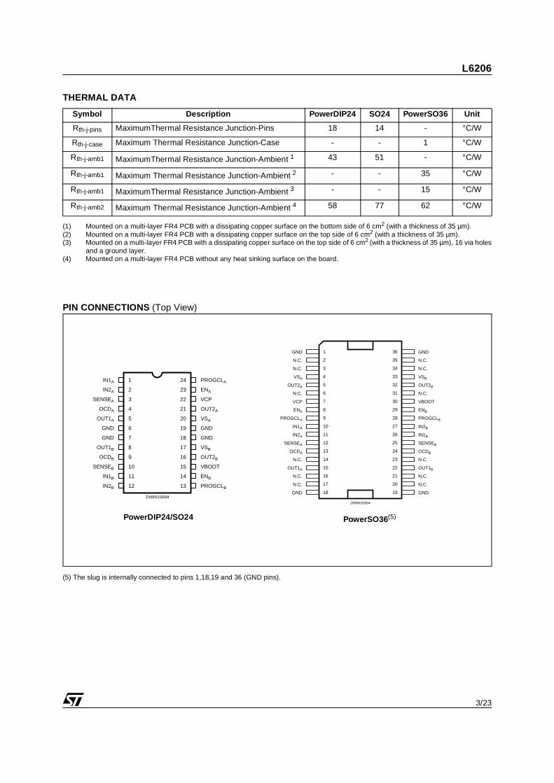
PIN CONNECTIONS (Top View)
(5) The slug is internally connected to pins 1,18,19 and 36 (GND pins).
Symbol Description PowerDIP24 SO24 PowerSO36 Unit
Rth-j-pins MaximumThermal Resistance Junction-Pins 18 14 - °C/W
Rth-j-case Maximum Thermal Resistance Junction-Case - - 1 °C/W
Rth-j-amb1 MaximumThermal Resistance Junction-Ambient 1
(1) Mounted on a multi-layer FR4 PCB with a dissipating copper surface on the bottom side of 6 cm2 (with a thickness of 35 µm).
43 51 - °C/W
Rth-j-amb1 Maximum Thermal Resistance Junction-Ambient 2
(2) Mounted on a multi-layer FR4 PCB with a dissipating copper surface on the top side of 6 cm2 (with a thickness of 35 µm).
- - 35 °C/W
Rth-j-amb1 MaximumThermal Resistance Junction-Ambient 3
(3) Mounted on a multi-layer FR4 PCB with a dissipating copper surface on the top side of 6 cm2 (with a thickness of 35 µm), 16 via holesand a ground layer.
- - 15 °C/W
Rth-j-amb2 Maximum Thermal Resistance Junction-Ambient 4
(4) Mounted on a multi-layer FR4 PCB without any heat sinking surface on the board.
58 77 62 °C/W
PowerDIP24/SO24 PowerSO36 (5)
GND
GND
OUT1B
OCDB
SENSEB
IN2B
IN1B
1
3
2
4
5
6
7
8
9
PROGCLB
VBOOT
ENB
OUT2B
VSB
GND
GND19
18
17
16
15
13
14
D99IN1089A
10
11
12
24
23
22
21
20
IN1A
IN2A
SENSEA
OCDA
OUT1A VSA
OUT2A
VCP
ENA
PROGCLA
GND
N.C.
N.C.
VSA
OCDA
OUT1A
N.C.
N.C.
N.C. N.C.
N.C.
OUT1B
OCDB
N.C.
VSB
N.C.
N.C.
GND
18
16
17
15
6
5
4
3
2
21
22
31
32
33
35
34
36
20
1
19GND GND
D99IN1090A
IN1A
SENSEA
IN2A
SENSEB
IN2B
IN1B
9
8
7
28
29
30
PROGCLA PROGCLB
10 27
OUT2A
ENA
VCP
ENB
OUT2B
VBOOT
14
12
11
23
25
26
N.C. N.C.
13 24
L6206
4/23
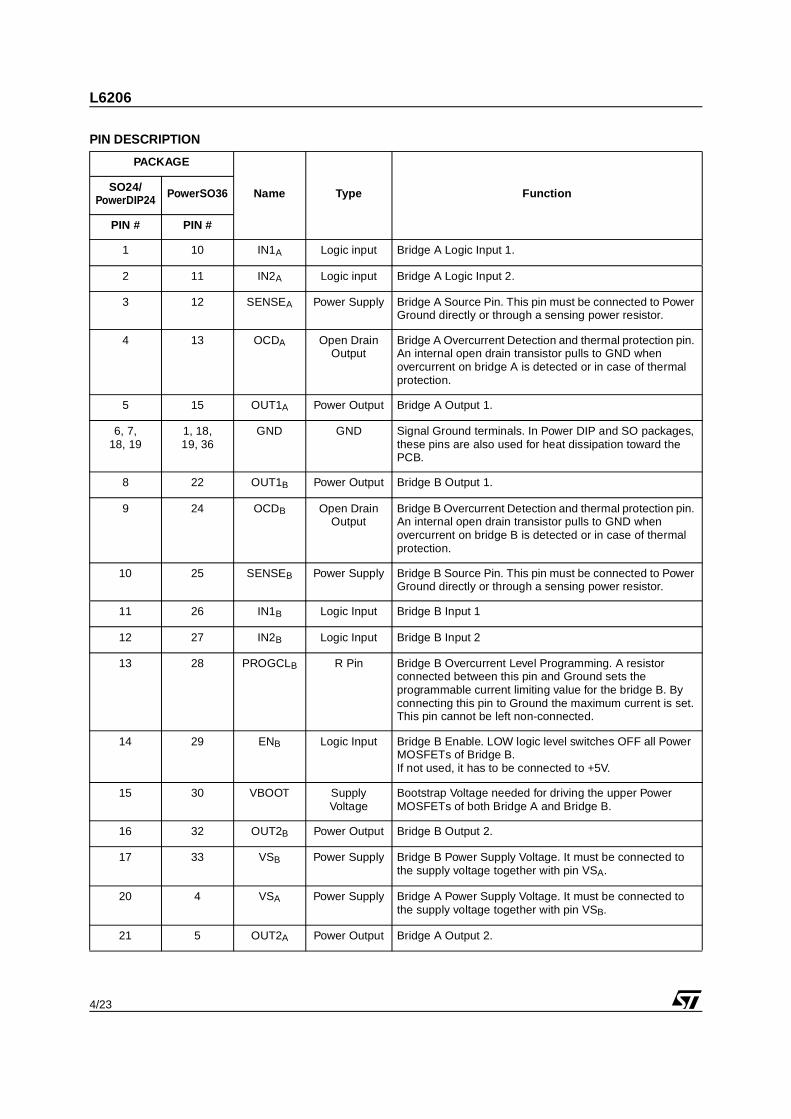
PIN DESCRIPTION
PACKAGE
Name Type FunctionSO24/PowerDIP24 PowerSO36
PIN # PIN #
1 10 IN1A Logic input Bridge A Logic Input 1.
2 11 IN2A Logic input Bridge A Logic Input 2.
3 12 SENSEA Power Supply Bridge A Source Pin. This pin must be connected to Power Ground directly or through a sensing power resistor.
4 13 OCDA Open Drain Output
Bridge A Overcurrent Detection and thermal protection pin. An internal open drain transistor pulls to GND when overcurrent on bridge A is detected or in case of thermal protection.
5 15 OUT1A Power Output Bridge A Output 1.
6, 7,18, 19
1, 18,19, 36
GND GND Signal Ground terminals. In Power DIP and SO packages, these pins are also used for heat dissipation toward the PCB.
8 22 OUT1B Power Output Bridge B Output 1.
9 24 OCDB Open Drain Output
Bridge B Overcurrent Detection and thermal protection pin. An internal open drain transistor pulls to GND when overcurrent on bridge B is detected or in case of thermal protection.
10 25 SENSEB Power Supply Bridge B Source Pin. This pin must be connected to Power Ground directly or through a sensing power resistor.
11 26 IN1B Logic Input Bridge B Input 1
12 27 IN2B Logic Input Bridge B Input 2
13 28 PROGCLB R Pin Bridge B Overcurrent Level Programming. A resistor connected between this pin and Ground sets the programmable current limiting value for the bridge B. By connecting this pin to Ground the maximum current is set. This pin cannot be left non-connected.
14 29 ENB Logic Input Bridge B Enable. LOW logic level switches OFF all Power MOSFETs of Bridge B.If not used, it has to be connected to +5V.
15 30 VBOOT Supply Voltage
Bootstrap Voltage needed for driving the upper Power MOSFETs of both Bridge A and Bridge B.
16 32 OUT2B Power Output Bridge B Output 2.
17 33 VSB Power Supply Bridge B Power Supply Voltage. It must be connected to the supply voltage together with pin VSA.
20 4 VSA Power Supply Bridge A Power Supply Voltage. It must be connected to the supply voltage together with pin VSB.
21 5 OUT2A Power Output Bridge A Output 2.
5/23
L6206
PACKAGE
Name Type FunctionSO24/PowerDIP24 PowerSO36
PIN # PIN #
22 7 VCP Output Charge Pump Oscillator Output.
23 8 ENA Logic Input Bridge A Enable. LOW logic level switches OFF all Power MOSFETs of Bridge A.If not used, it has to be connected to +5V.
24 9 PROGCLA R Pin Bridge A Overcurrent Level Programming. A resistor connected between this pin and Ground sets the programmable current limiting value for the bridge A. By connecting this pin to Ground the maximum current is set. This pin cannot be left non-connected.
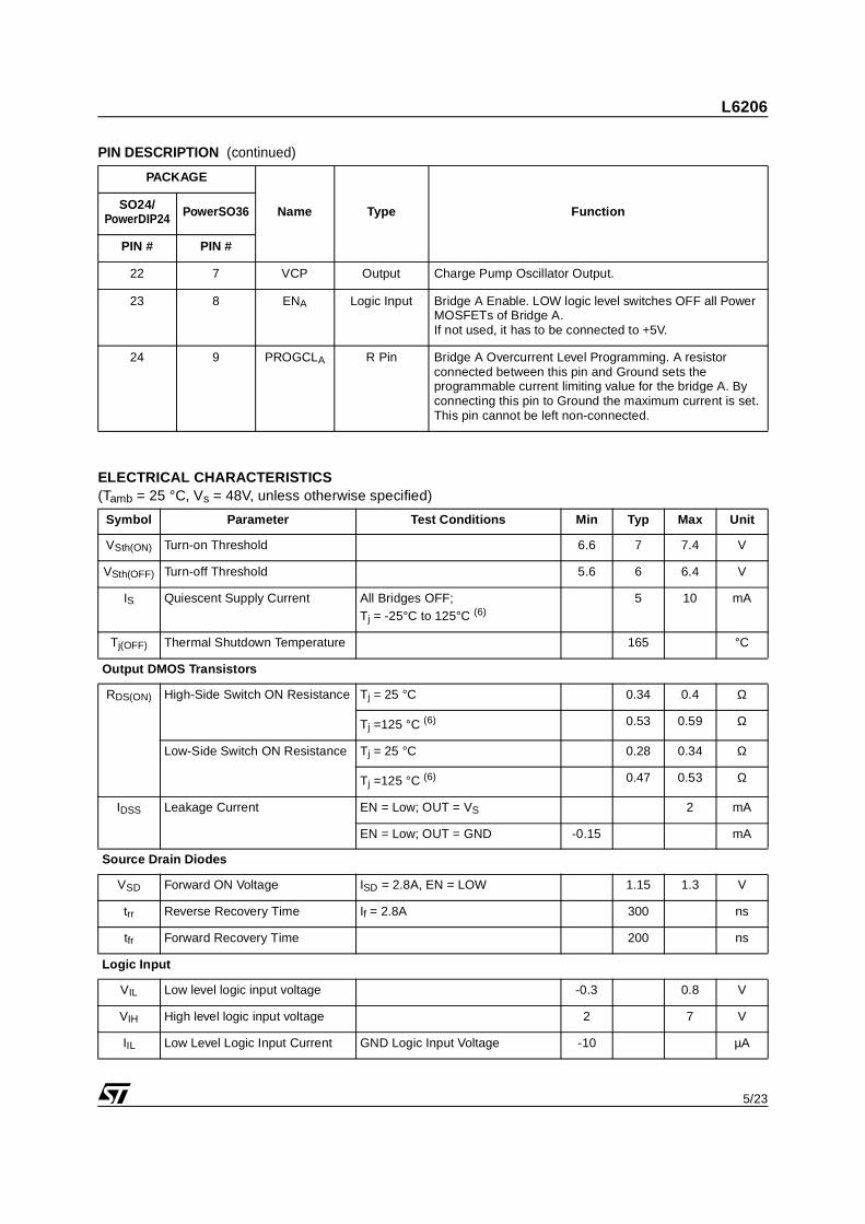
ELECTRICAL CHARACTERISTICS (Tamb = 25 °C, Vs = 48V, unless otherwise specified)
Symbol Parameter Test Conditions Min Typ Max Unit
VSth(ON) Turn-on Threshold 6.6 7 7.4 V
VSth(OFF) Turn-off Threshold 5.6 6 6.4 V
IS Quiescent Supply Current All Bridges OFF;Tj = -25°C to 125°C (6)
5 10 mA
Tj(OFF) Thermal Shutdown Temperature 165 °C
Output DMOS Transistors
RDS(ON) High-Side Switch ON Resistance Tj = 25 °C 0.34 0.4 Ω
Tj =125 °C (6) 0.53 0.59 Ω
Low-Side Switch ON Resistance Tj = 25 °C 0.28 0.34 Ω
Tj =125 °C (6) 0.47 0.53 Ω
IDSS Leakage Current EN = Low; OUT = VS 2 mA
EN = Low; OUT = GND -0.15 mA
Source Drain Diodes
VSD Forward ON Voltage ISD = 2.8A, EN = LOW 1.15 1.3 V
trr Reverse Recovery Time If = 2.8A 300 ns
tfr Forward Recovery Time 200 ns
Logic Input
VIL Low level logic input voltage -0.3 0.8 V
VIH High level logic input voltage 2 7 V
IIL Low Level Logic Input Current GND Logic Input Voltage -10 µA
PIN DESCRIPTION (continued)
L6206
6/23
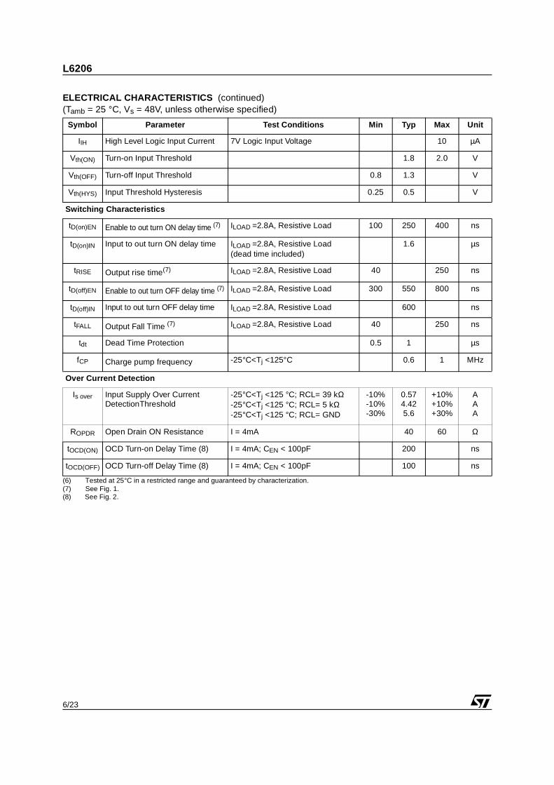
(6) Tested at 25°C in a restricted range and guaranteed by characterization.(7) See Fig. 1.(8) See Fig. 2.
IIH High Level Logic Input Current 7V Logic Input Voltage 10 µA
Vth(ON) Turn-on Input Threshold 1.8 2.0 V
Vth(OFF) Turn-off Input Threshold 0.8 1.3 V
Vth(HYS) Input Threshold Hysteresis 0.25 0.5 V
Switching Characteristics
tD(on)EN Enable to out turn ON delay time (7) ILOAD =2.8A, Resistive Load 100 250 400 ns
tD(on)IN Input to out turn ON delay time ILOAD =2.8A, Resistive Load(dead time included)
1.6 µs
tRISE Output rise time(7) ILOAD =2.8A, Resistive Load 40 250 ns
tD(off)EN Enable to out turn OFF delay time (7) ILOAD =2.8A, Resistive Load 300 550 800 ns
tD(off)IN Input to out turn OFF delay time ILOAD =2.8A, Resistive Load 600 ns
tFALL Output Fall Time (7) ILOAD =2.8A, Resistive Load 40 250 ns
tdt Dead Time Protection 0.5 1 µs
fCP Charge pump frequency -25°C<Tj <125°C 0.6 1 MHz
Over Current Detection
Is over Input Supply Over Current DetectionThreshold
-25°C<Tj <125 °C; RCL= 39 kΩ-25°C<Tj <125 °C; RCL= 5 kΩ-25°C<Tj <125 °C; RCL= GND
-10%-10%-30%
0.574.425.6
+10%+10%+30%
AAA
ROPDR Open Drain ON Resistance I = 4mA 40 60 Ω
tOCD(ON) OCD Turn-on Delay Time (8) I = 4mA; CEN < 100pF 200 ns
tOCD(OFF) OCD Turn-off Delay Time (8) I = 4mA; CEN < 100pF 100 ns
ELECTRICAL CHARACTERISTICS (continued)(Tamb = 25 °C, Vs = 48V, unless otherwise specified)
Symbol Parameter Test Conditions Min Typ Max Unit
7/23
L6206
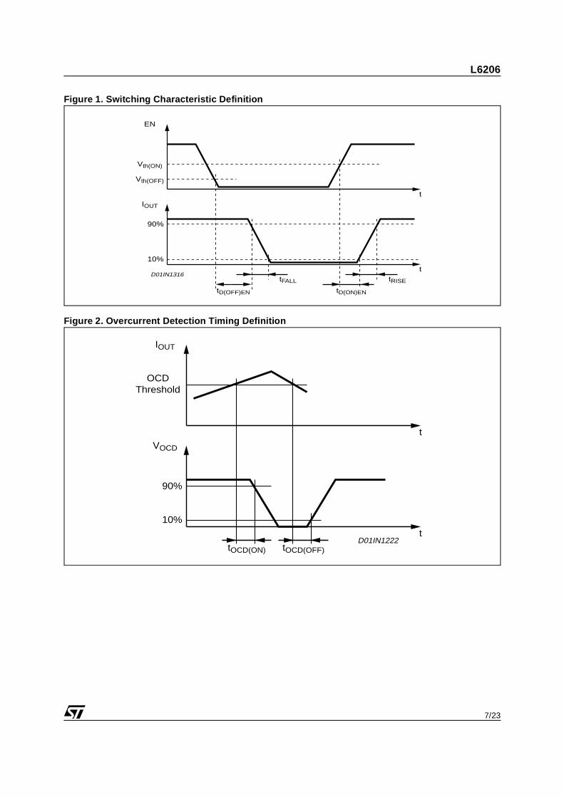
Figure 1. Switching Characteristic Definition
Figure 2. Overcurrent Detection Timing Definition
Vth(ON)
Vth(OFF)
90%
10%
EN
IOUT
t
ttFALL
tD(OFF)EN
tRISE
tD(ON)EN
D01IN1316
OCDThreshold
90%
10%
IOUT
VOCD
t
t
tOCD(OFF)tOCD(ON)D01IN1222
L6206
8/23
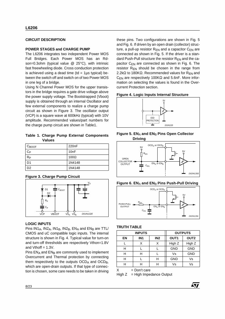
CIRCUIT DESCRIPTION
POWER STAGES and CHARGE PUMPThe L6206 integrates two independent Power MOSFull Bridges. Each Power MOS has an Rd-son=0.3ohm (typical value @ 25°C), with intrinsicfast freewheeling diode. Cross conduction protectionis achieved using a dead time (td = 1µs typical) be-tween the switch off and switch on of two Power MOSin one leg of a bridge.Using N Channel Power MOS for the upper transis-tors in the bridge requires a gate drive voltage abovethe power supply voltage. The Bootstrapped (Vboot)supply is obtained through an internal Oscillator andfew external components to realize a charge pumpcircuit as shown in Figure 3. The oscillator output(VCP) is a square wave at 600kHz (typical) with 10Vamplitude. Recommended values/part numbers forthe charge pump circuit are shown in Table1.
Table 1. Charge Pump External ComponentsValues
Figure 3. Charge Pump Circuit
LOGIC INPUTSPins IN1A, IN2A, IN1B, IN2B, ENA and ENB are TTL/CMOS and uC compatible logic inputs. The internalstructure is shown in Fig. 4. Typical value for turn-onand turn-off thresholds are respectively Vthon=1.8Vand Vthoff = 1.3V.Pins ENA and ENB are commonly used to implementOvercurrent and Thermal protection by connectingthem respectively to the outputs OCDA and OCDB,which are open-drain outputs. If that type of connec-tion is chosen, some care needs to be taken in driving
these pins. Two configurations are shown in Fig. 5and Fig. 6. If driven by an open drain (collector) struc-ture, a pull-up resistor REN and a capacitor CEN areconnected as shown in Fig. 5. If the driver is a stan-dard Push-Pull structure the resistor REN and the ca-pacitor CEN are connected as shown in Fig. 6. Theresistor REN should be chosen in the range from2.2kΩ to 180KΩ. Recommended values for REN andCEN are respectively 100KΩ and 5.6nF. More infor-mation on selecting the values is found in the Over-current Protection section.
Figure 4. Logic Inputs Internal Structure
Figure 5. EN A and ENB Pins Open Collector Driving
Figure 6. EN A and ENB Pins Push-Pull Driving
TRUTH TABLE
X = Don't careHigh Z = High Impedance Output
CBOOT 220nF
CP 10nF
RP 100Ω
D1 1N4148
D2 1N4148
D2
CBOOTD1
RP
CP
VS
VSAVCP VBOOT VSB D01IN1328
INPUTS OUTPUTS
EN IN1 IN2 OUT1 OUT2
L X X High Z High Z
H L L GND GND
H H L Vs GND
H L H GND Vs
H H H Vs Vs
5V
D01IN1329
ESDPROTECTION
5V
5V
OPENCOLLECTOR
OUTPUT
REN
CEN
ENA or ENB
OCDA or OCDB
D02IN1355
5V
PUSH-PULLOUTPUT
REN
CEN
ENA or ENB
D02IN1356
OCDA or OCDB
9/23
L6206
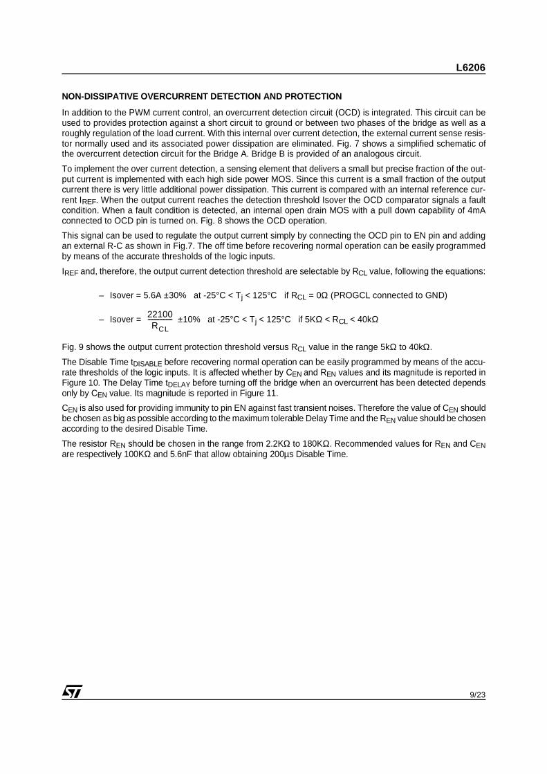
NON-DISSIPATIVE OVERCURRENT DETECTION AND PROTECTION
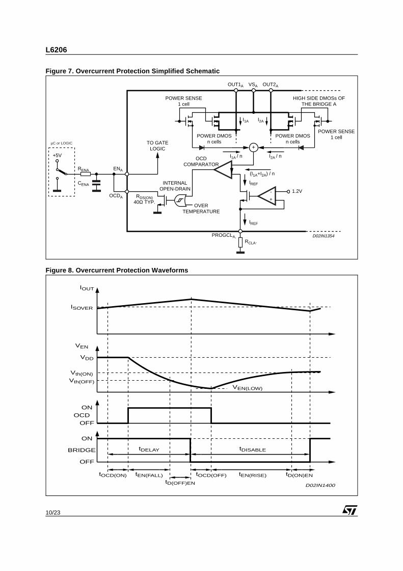
In addition to the PWM current control, an overcurrent detection circuit (OCD) is integrated. This circuit can beused to provides protection against a short circuit to ground or between two phases of the bridge as well as aroughly regulation of the load current. With this internal over current detection, the external current sense resis-tor normally used and its associated power dissipation are eliminated. Fig. 7 shows a simplified schematic ofthe overcurrent detection circuit for the Bridge A. Bridge B is provided of an analogous circuit.
To implement the over current detection, a sensing element that delivers a small but precise fraction of the out-put current is implemented with each high side power MOS. Since this current is a small fraction of the outputcurrent there is very little additional power dissipation. This current is compared with an internal reference cur-rent IREF. When the output current reaches the detection threshold Isover the OCD comparator signals a faultcondition. When a fault condition is detected, an internal open drain MOS with a pull down capability of 4mAconnected to OCD pin is turned on. Fig. 8 shows the OCD operation.
This signal can be used to regulate the output current simply by connecting the OCD pin to EN pin and addingan external R-C as shown in Fig.7. The off time before recovering normal operation can be easily programmedby means of the accurate thresholds of the logic inputs.
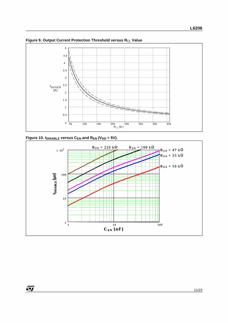
IREF and, therefore, the output current detection threshold are selectable by RCL value, following the equations:
– Isover = 5.6A ±30% at -25°C < Tj < 125°C if RCL = 0Ω (PROGCL connected to GND)
– Isover = ±10% at -25°C < Tj < 125°C if 5KΩ < RCL < 40kΩ
Fig. 9 shows the output current protection threshold versus RCL value in the range 5kΩ to 40kΩ.
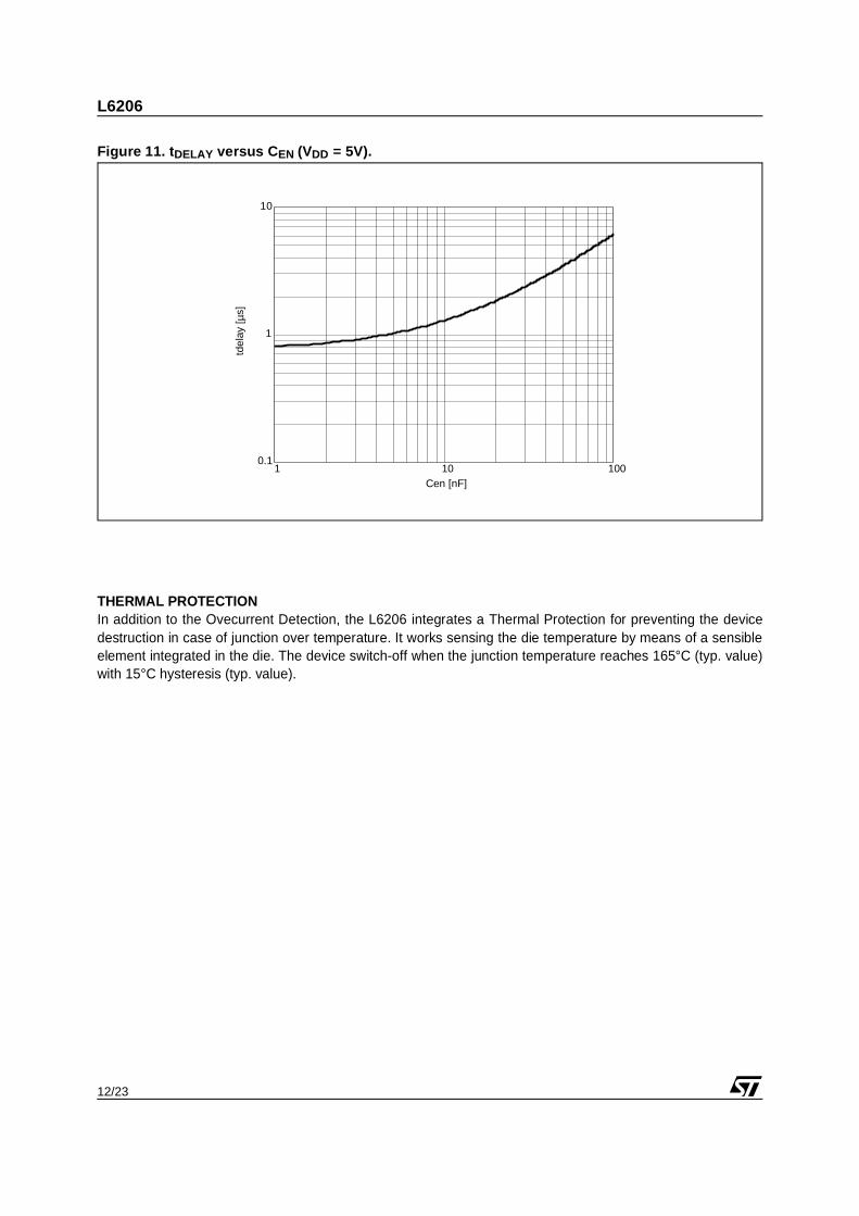
The Disable Time tDISABLE before recovering normal operation can be easily programmed by means of the accu-rate thresholds of the logic inputs. It is affected whether by CEN and REN values and its magnitude is reported inFigure 10. The Delay Time tDELAY before turning off the bridge when an overcurrent has been detected dependsonly by CEN value. Its magnitude is reported in Figure 11.
CEN is also used for providing immunity to pin EN against fast transient noises. Therefore the value of CEN shouldbe chosen as big as possible according to the maximum tolerable Delay Time and the REN value should be chosenaccording to the desired Disable Time.
The resistor REN should be chosen in the range from 2.2KΩ to 180KΩ. Recommended values for REN and CENare respectively 100KΩ and 5.6nF that allow obtaining 200µs Disable Time.
22100RCL
----------------
L6206
10/23
Figure 7. Overcurrent Protection Simplified Schematic
Figure 8. Overcurrent Protection Waveforms
+
OVERTEMPERATURE
IREF
IREF
(I1A+I2A) / n
I1A / n
POWER SENSE1 cell
POWER SENSE1 cellPOWER DMOS
n cellsPOWER DMOS
n cells
HIGH SIDE DMOSs OFTHE BRIDGE A
OUT1A OUT2A VSA
I1A I2A
I2A / nOCDCOMPARATOR
TO GATELOGIC
INTERNALOPEN-DRAIN
RDS(ON)40Ω TYP.
CENA
RENA
RCLA.
ENA
OCDA
PROGCLA,
+5V
1.2V-
+
µC or LOGIC
D02IN1354
ISOVER
IOUT
Vth(ON)
Vth(OFF)VEN(LOW)
VDD
tOCD(ON) tD(ON)ENtEN(FALL) tEN(RISE)
tDISABLEtDELAY
tOCD(OFF)
tD(OFF)EN
VEN
BRIDGE
ON
OFF
OCDON
OFF
D02IN1400
11/23
L6206
Figure 9. Output Current Protection Threshold versus R CL Value
Figure 10. t DISABLE versus C EN and REN (VDD = 5V).
5k 10k 15k 20k 25k 30k 35k 40k 0
0.5
1
1.5
2
2.5
3
3.5
5
R CL [ Ω ]
4
4.5
I SOVER [A]
1 10 1001
10
100
1 .103
C E N [n F ]
t DIS
AB
LE[µ
s]
R E N = 2 20 kΩ R E N = 1 00 kΩR E N = 4 7 kΩR E N = 3 3 kΩ
R E N = 1 0 kΩ
1 10 1001
10
100
1 .103
C E N [n F ]
t DIS
AB
LE[µ
s]
R E N = 2 20 kΩ R E N = 1 00 kΩR E N = 4 7 kΩR E N = 3 3 kΩ
R E N = 1 0 kΩ
L6206
12/23
Figure 11. t DELAY versus C EN (VDD = 5V).
THERMAL PROTECTIONIn addition to the Ovecurrent Detection, the L6206 integrates a Thermal Protection for preventing the devicedestruction in case of junction over temperature. It works sensing the die temperature by means of a sensibleelement integrated in the die. The device switch-off when the junction temperature reaches 165°C (typ. value)with 15°C hysteresis (typ. value).
1 10 1000.1
1
10
Cen [nF]
tdel
ay [ µ
s]
13/23
L6206
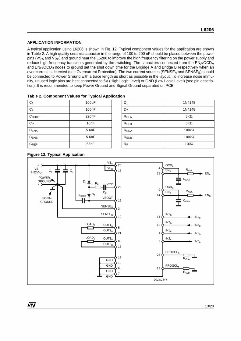
APPLICATION INFORMATION
A typical application using L6206 is shown in Fig. 12. Typical component values for the application are shownin Table 2. A high quality ceramic capacitor in the range of 100 to 200 nF should be placed between the powerpins (VSA and VSB) and ground near the L6206 to improve the high frequency filtering on the power supply andreduce high frequency transients generated by the switching. The capacitors connected from the ENA/OCDAand ENB/OCDB nodes to ground set the shut down time for the Brgidge A and Bridge B respectively when anover current is detected (see Overcurrent Protection). The two current sources (SENSEA and SENSEB) shouldbe connected to Power Ground with a trace length as short as possible in the layout. To increase noise immu-nity, unused logic pins are best connected to 5V (High Logic Level) or GND (Low Logic Level) (see pin descrip-tion). It is recommended to keep Power Ground and Signal Ground separated on PCB.
Table 2. Component Values for Typical Application
Figure 12. Typical Application
C1 100uF D1 1N4148
C2 100nF D2 1N4148
CBOOT 220nF RCLA 5KΩ
CP 10nF RCLB 5KΩ
CENA 5.6nF RENA 100kΩ
CENB 5.6nF RENB 100kΩ
CREF 68nF RP 100Ω
CPCBOOT
RP
D2
D1
C2
OUT1ALOADA
LOADB
OCDA
OCDB
1
5
21
18
19
8
16
OUT2A
GND
GND
GND
GND
PROGCLA
OUT2B
OUT1B
VSA
POWERGROUND
SIGNALGROUND
+
-
VS8-52VDC
4VSB
VCP
VBOOT
C1
SENSEA
20
IN1A
IN2A
IN1A
IN2A2
6
7
9
ENA
ENB
CENB
RENB
RENAENA
ENB
23
IN2B12
IN1B
IN2B
IN1B11
14
24
17
3
15
22
SENSEB
RCLA
10
CENA
PROGCLB13
RCLB
D02IN1344
L6206
14/23
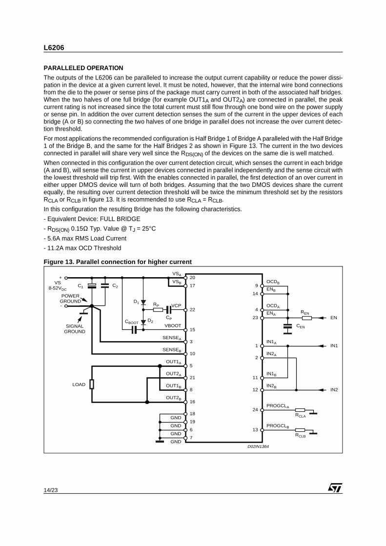
PARALLELED OPERATION
The outputs of the L6206 can be paralleled to increase the output current capability or reduce the power dissi-pation in the device at a given current level. It must be noted, however, that the internal wire bond connectionsfrom the die to the power or sense pins of the package must carry current in both of the associated half bridges.When the two halves of one full bridge (for example OUT1A and OUT2A) are connected in parallel, the peakcurrent rating is not increased since the total current must still flow through one bond wire on the power supplyor sense pin. In addition the over current detection senses the sum of the current in the upper devices of eachbridge (A or B) so connecting the two halves of one bridge in parallel does not increase the over current detec-tion threshold.
For most applications the recommended configuration is Half Bridge 1 of Bridge A paralleled with the Half Bridge1 of the Bridge B, and the same for the Half Bridges 2 as shown in Figure 13. The current in the two devicesconnected in parallel will share very well since the RDS(ON) of the devices on the same die is well matched.
When connected in this configuration the over current detection circuit, which senses the current in each bridge(A and B), will sense the current in upper devices connected in parallel independently and the sense circuit withthe lowest threshold will trip first. With the enables connected in parallel, the first detection of an over current ineither upper DMOS device will turn of both bridges. Assuming that the two DMOS devices share the currentequally, the resulting over current detection threshold will be twice the minimum threshold set by the resistorsRCLA or RCLB in figure 13. It is recommended to use RCLA = RCLB.
In this configuration the resulting Bridge has the following characteristics.
- Equivalent Device: FULL BRIDGE
- RDS(ON) 0.15Ω Typ. Value @ TJ = 25°C
- 5.6A max RMS Load Current
- 11.2A max OCD Threshold
Figure 13. Parallel connection for higher current
CPCBOOT
RP
D2
D1
C2
OUT1A
LOAD
OCDA
OCDB
1
5
21
18
19
8
16
OUT2A
GND
GND
GND
GND
PROGCLA
OUT2B
OUT1B
VSA
POWERGROUND
SIGNALGROUND
+
-
VS8-52VDC
4
VSB
VCP
VBOOT
C1
SENSEA
20
IN2
IN1A
IN2B12
6
7
9
ENA
ENB
RENEN23
IN1B11
IN2A
IN1
2
14
24
17
3
15
22
SENSEB
RCLA
10
CEN
PROGCLB13
RCLB
D02IN1364
15/23
L6206
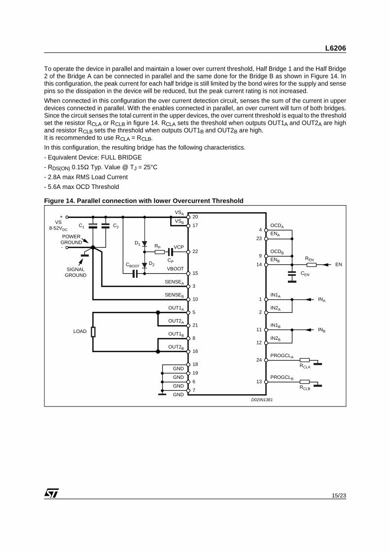
To operate the device in parallel and maintain a lower over current threshold, Half Bridge 1 and the Half Bridge2 of the Bridge A can be connected in parallel and the same done for the Bridge B as shown in Figure 14. Inthis configuration, the peak current for each half bridge is still limited by the bond wires for the supply and sensepins so the dissipation in the device will be reduced, but the peak current rating is not increased.
When connected in this configuration the over current detection circuit, senses the sum of the current in upperdevices connected in parallel. With the enables connected in parallel, an over current will turn of both bridges.Since the circuit senses the total current in the upper devices, the over current threshold is equal to the thresholdset the resistor RCLA or RCLB in figure 14. RCLA sets the threshold when outputs OUT1A and OUT2A are highand resistor RCLB sets the threshold when outputs OUT1B and OUT2B are high.It is recommended to use RCLA = RCLB.
In this configuration, the resulting bridge has the following characteristics.
- Equivalent Device: FULL BRIDGE
- RDS(ON) 0.15Ω Typ. Value @ TJ = 25°C
- 2.8A max RMS Load Current
- 5.6A max OCD Threshold
Figure 14. Parallel connection with lower Overcurrent Threshold
CPCBOOT
RP
D2
D1
C2
OUT1A
LOAD
OCDA
OCDB
1
5
21
18
19
8
16
OUT2A
GND
GND
GND
GND
PROGCLA
OUT2B
OUT1B
VSA
POWERGROUND
SIGNALGROUND
+
-
VS8-52VDC 4
VSB
VCP
VBOOT
C1
SENSEA
20
INA
IN1A
IN2A2
6
7
9
ENA
ENB
CEN
RENEN
23
IN2B12
IN1BINB11
14
24
17
3
15
22
SENSEB
RCLA
10
PROGCLB13
RCLB
D02IN1361
L6206
16/23
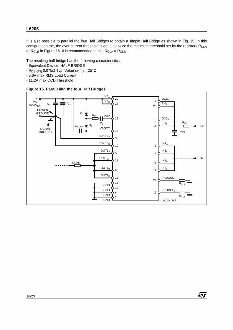
It is also possible to parallel the four Half Bridges to obtain a simple Half Bridge as shown in Fig. 15. In thisconfiguration the, the over current threshold is equal to twice the minimum threshold set by the resistors RCLAor RCLB in Figure 15. It is recommended to use RCLA = RCLB.
The resulting half bridge has the following characteristics. - Equivalent Device: HALF BRIDGE- RDS(ON) 0.075Ω Typ. Value @ TJ = 25°C- 5.6A max RMS Load Current- 11.2A max OCD Threshold
Figure 15. Paralleling the four Half Bridges
CPCBOOT
RP
D2
D1
C2
OUT1A
LOAD
OCDA
OCDB
1
5
21
18
19
8
16
OUT2A
GND
GND
GND
GND
PROGCLA
OUT2B
OUT1B
VSA
POWERGROUND
SIGNALGROUND
+
-
VS8-52VDC
4VSB
VCP
VBOOT
C1
SENSEA
20
IN
IN1A
IN2A2
6
7
9
ENA
ENB
CEN
RENEN
23
IN2B12
IN1B11
14
24
17
3
15
22
SENSEB
RCLA
10
PROGCLB13
RCLB
D02IN1365
17/23
L6206
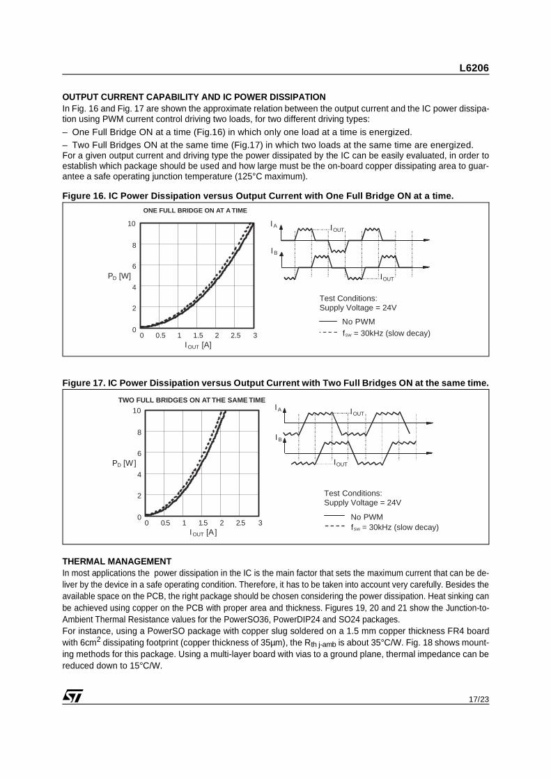
OUTPUT CURRENT CAPABILITY AND IC POWER DISSIPATIONIn Fig. 16 and Fig. 17 are shown the approximate relation between the output current and the IC power dissipa-tion using PWM current control driving two loads, for two different driving types:– One Full Bridge ON at a time (Fig.16) in which only one load at a time is energized.– Two Full Bridges ON at the same time (Fig.17) in which two loads at the same time are energized.For a given output current and driving type the power dissipated by the IC can be easily evaluated, in order toestablish which package should be used and how large must be the on-board copper dissipating area to guar-antee a safe operating junction temperature (125°C maximum).
Figure 16. IC Power Dissipation versus Output Current with One Full Bridge ON at a time.
Figure 17. IC Power Dissipation versus Output Current with Two Full Bridges ON at the same time.
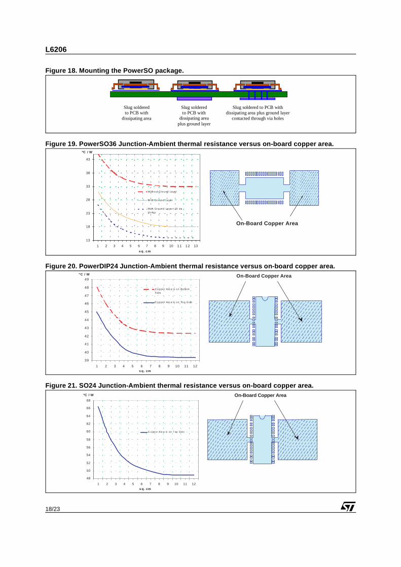
THERMAL MANAGEMENTIn most applications the power dissipation in the IC is the main factor that sets the maximum current that can be de-liver by the device in a safe operating condition. Therefore, it has to be taken into account very carefully. Besides theavailable space on the PCB, the right package should be chosen considering the power dissipation. Heat sinking canbe achieved using copper on the PCB with proper area and thickness. Figures 19, 20 and 21 show the Junction-to-Ambient Thermal Resistance values for the PowerSO36, PowerDIP24 and SO24 packages. For instance, using a PowerSO package with copper slug soldered on a 1.5 mm copper thickness FR4 boardwith 6cm2 dissipating footprint (copper thickness of 35µm), the Rth j-amb is about 35°C/W. Fig. 18 shows mount-ing methods for this package. Using a multi-layer board with vias to a ground plane, thermal impedance can bereduced down to 15°C/W.
No PWMfSW = 30kHz (slow decay)
Test Conditions:Supply Voltage = 24V
IA
IB
IOUT
IOUT
0 0.5 1 1.5 2 2.5 30
2
4
6
8
10
PD [W]
IOUT [A]
ONE FULL BRIDGE ON AT A TIME
No PWMfSW = 30kHz (slow decay)
Test Conditions:Supply Voltage = 24V
IA
IB
IOUT
IOUT
0 0.5 1 1.5 2 2.5 30
2
4
6
8
10
PD [W]
IOUT [A]
TWO FULL BRIDGES ON AT THE SAME TIME
L6206
18/23
Figure 18. Mounting the PowerSO package.
Figure 19. PowerSO36 Junction-Ambient thermal resistance versus on-board copper area.
Figure 20. PowerDIP24 Junction-Ambient thermal resistance versus on-board copper area.
Figure 21. SO24 Junction-Ambient thermal resistance versus on-board copper area.
Slug soldered to PCB with
dissipating area
Slug soldered to PCB with
dissipating area plus ground layer
Slug soldered to PCB with dissipating area plus ground layer
contacted through via holes
13
18
23
28
33
38
43
1 2 3 4 5 6 7 8 9 10 11 12 13
W ith o ut G ro u nd La yer
W ith Gro un d La yer
W ith Gro un d La yer+16 viaH o le s
s q. cm
ºC / W
On-Board Copper Area
39
40
41
42
43
44
45
46
47
48
49
1 2 3 4 5 6 7 8 9 10 11 12
Co p pe r Are a is o n Bo tto mS id e
Co p pe r Are a is o n To p S ide
s q. cm
ºC / W On-Board Copper Area
48
50
52
54
56
58
60
62
64
66
68
1 2 3 4 5 6 7 8 9 10 11 12
C o pp er Are a is on T op Sid e
s q. cm
ºC / W On-Board Copper Area
19/23
L6206
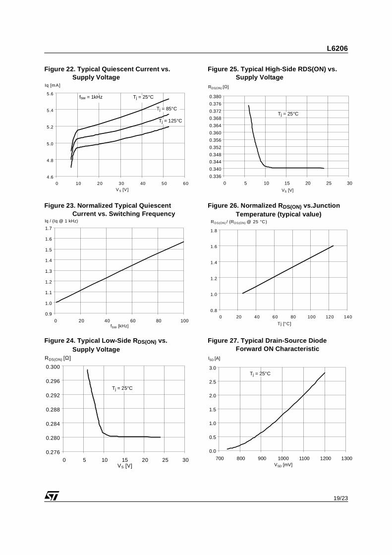
Figure 22. Typical Quiescent Current vs. Supply Voltage
Figure 23. Normalized Typical Quiescent Current vs. Switching Frequency
Figure 24. Typical Low-Side R DS(ON) vs. Supply Voltage
Figure 25. Typical High-Side RDS(ON) vs. Supply Voltage
Figure 26. Normalized R DS(ON) vs.Junction Temperature (typical value)
Figure 27. Typical Drain-Source Diode Forward ON Characteristic
4.6
4.8
5.0
5.2
5.4
5.6
0 10 20 30 40 50 60
Iq [mA]
VS [V]
fsw = 1kHz Tj = 25°C
Tj = 85°C
Tj = 125°C
0.9
1.0
1.1
1.2
1.3
1.4
1.5
1.6
1.7
0 20 40 60 80 100
Iq / (Iq @ 1 kHz)
fSW [kHz]
0.276
0.280
0.284
0.288
0.292
0.296
0.300
0 5 10 15 20 25 30
RDS(ON) [Ω]
VS [V]
Tj = 25°C
0.336
0.340
0.344
0.348
0.352
0.356
0.360
0.364
0.368
0.372
0.376
0.380
0 5 10 15 20 25 30
RDS(ON) [Ω]
VS [V]
Tj = 25°C
0.8
1.0
1.2
1.4
1.6
1.8
0 20 40 60 80 100 120 140
RDS(ON) / (RDS(ON) @ 25 °C)
Tj [°C]
0.0
0.5
1.0
1.5
2.0
2.5
3.0
700 800 900 1000 1100 1200 1300
ISD [A]
VSD [mV]
Tj = 25°C
L6206
20/23
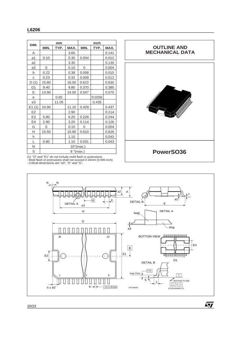
DIM.mm inch
MIN. TYP. MAX. MIN. TYP. MAX.
A 3.60 0.141
a1 0.10 0.30 0.004 0.012
a2 3.30 0.130
a3 0 0.10 0 0.004
b 0.22 0.38 0.008 0.015
c 0.23 0.32 0.009 0.012
D (1) 15.80 16.00 0.622 0.630
D1 9.40 9.80 0.370 0.385
E 13.90 14.50 0.547 0.570
e 0.65 0.0256
e3 11.05 0.435
E1 (1) 10.90 11.10 0.429 0.437
E2 2.90 0.114
E3 5.80 6.20 0.228 0.244
E4 2.90 3.20 0.114 0.126
G 0 0.10 0 0.004
H 15.50 15.90 0.610 0.626
h 1.10 0.043
L 0.80 1.10 0.031 0.043
N 10°(max.)
S 8 °(max.)
(1): "D" and "E1" do not include mold flash or protrusions- Mold flash or protrusions shall not exceed 0.15mm (0.006 inch)- Critical dimensions are "a3", "E" and "G".
PowerSO36
e
a2 A
E
a1
PSO36MEC
DETAIL A
D
1 1 8
1936
E1E2
h x 45˚
DETAIL Alead
sluga3
S
Gage Plane0.35
L
DETAIL B
DETAIL B
(COPLANARITY)
G C
- C -
SEATING PLANE
e3
c
NN
⊕ M0.12 A Bb
B
A
H
E3
D1
BOTTOM VIEW
OUTLINE ANDMECHANICAL DATA
21/23
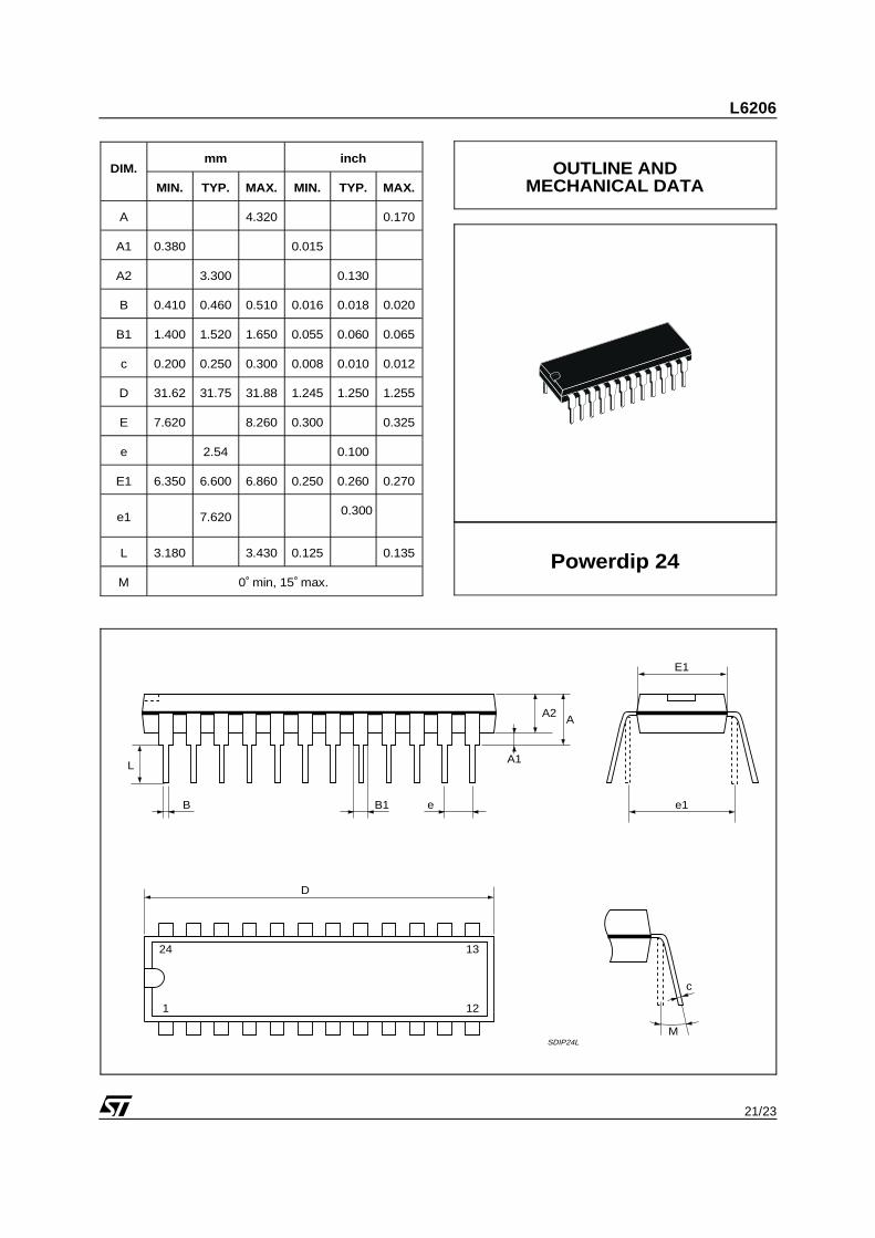
L6206
DIM.mm inch
MIN. TYP. MAX. MIN. TYP. MAX.
A 4.320 0.170
A1 0.380 0.015
A2 3.300 0.130
B 0.410 0.460 0.510 0.016 0.018 0.020
B1 1.400 1.520 1.650 0.055 0.060 0.065
c 0.200 0.250 0.300 0.008 0.010 0.012
D 31.62 31.75 31.88 1.245 1.250 1.255
E 7.620 8.260 0.300 0.325
e 2.54 0.100
E1 6.350 6.600 6.860 0.250 0.260 0.270
e1 7.620 0.300
L 3.180 3.430 0.125 0.135
M 0 min, 15 max.
Powerdip 24
A1
B eB1
D
13
12
24
1
L
A
e1
A2
c
E1
SDIP24LM
OUTLINE ANDMECHANICAL DATA
L6206
22/23
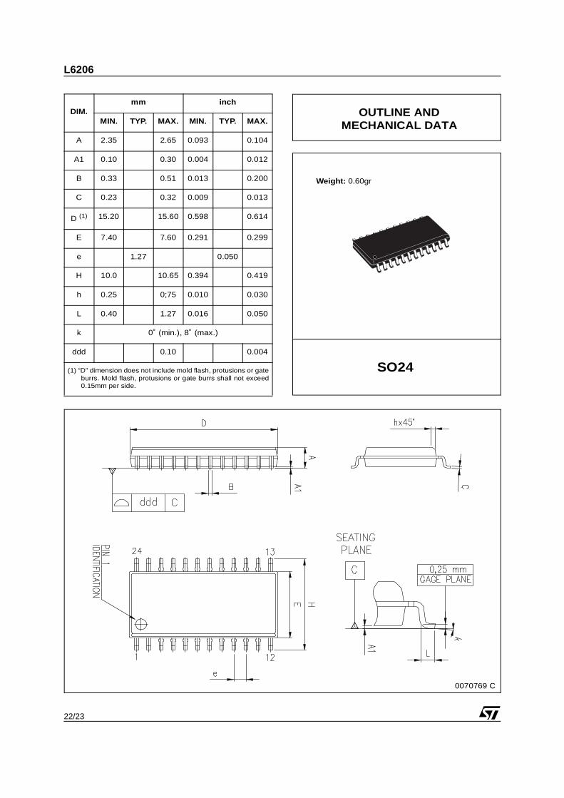
OUTLINE ANDMECHANICAL DATA
DIM.mm inch
MIN. TYP. MAX. MIN. TYP. MAX.
A 2.35 2.65 0.093 0.104
A1 0.10 0.30 0.004 0.012
B 0.33 0.51 0.013 0.200
C 0.23 0.32 0.009 0.013
D (1) 15.20 15.60 0.598 0.614
E 7.40 7.60 0.291 0.299
e 1.27 0.050
H 10.0 10.65 0.394 0.419
h 0.25 0;75 0.010 0.030
L 0.40 1.27 0.016 0.050
k 0˚ (min.), 8˚ (max.)
ddd 0.10 0.004
(1) “D” dimension does not include mold flash, protusions or gateburrs. Mold flash, protusions or gate burrs shall not exceed0.15mm per side.
SO24
0070769 C
Weight: 0.60gr

Information furnished is believed to be accurate and reliable. However, STMicroelectronics assumes no responsibility for the consequencesof use of such information nor for any infringement of patents or other rights of third parties which may result from its use. No license is grantedby implication or otherwise under any patent or patent rights of STMicroelectronics. Specifications mentioned in this publication are subjectto change without notice. This publication supersedes and replaces all information previously supplied. STMicroelectronics products are notauthorized for use as critical components in life support devices or systems without express written approval of STMicroelectronics.
The ST logo is a registered trademark of STMicroelectronics.All other names are the property of their respective owners
© 2003 STMicroelectronics - All rights reserved
STMicroelectronics GROUP OF COMPANIESAustralia - Belgium - Brazil - Canada - China - Czech Republic - Finland - France - Germany - Hong Kong - India - Israel - Italy - Japan -
Malaysia - Malta - Morocco - Singapore - Spain - Sweden - Switzerland - United Kingdom - United Stateswww.st.com
23/23
L6206


![IC-7800 Instruction Manual - · PDF file(p. 2-5) External transverter input/output connector. Activated by voltage applied to [ACC 2] pin 6, or when the transverter function is in](https://static.fdocument.org/doc/165x107/5a793a3f7f8b9ac53b8c4853/ic-7800-instruction-manual-p-2-5-external-transverter-inputoutput-connector.jpg)