
DLP9500 DLP 0.95 1080p Type A DMD (Rev. C) · PDF file7 Specifications ... 8.2 Functional...
54
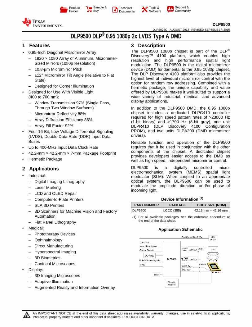
Product Folder Sample & Buy Technical Documents Tools & Software Support & Community DLP9500 DLPS025C – AUGUST 2012 – REVISED SEPTEMBER 2015 DLP9500 DLP ® 0.95 1080p 2x LVDS Type A DMD 1 Features 3 Description The DLP9500 1080p chipset is part of the DLP ® 1• 0.95-Inch Diagonal Micromirror Array Discovery™ 4100 platform, which enables high – 1920 × 1080 Array of Aluminum, Micrometer- resolution and high performance spatial light Sized Mirrors (1080p Resolution) modulation. The DLP9500 is the digital micromirror – 10.8-μm Micromirror Pitch device (DMD) fundamental to the 0.95 1080p chipset. The DLP Discovery 4100 platform also provides the – ±12° Micromirror Tilt Angle (Relative to Flat highest level of individual micromirror control with the State) option for random row addressing. Combined with a – Designed for Corner Illumination hermetic package, the unique capability and value • Designed for Use With Visible Light offered by DLP9500 makes it well suited to support a wide variety of industrial, medical, and advanced (400 to 700 nm): display applications. – Window Transmission 97% (Single Pass, Through Two Window Surfaces) In addition to the DLP9500 DMD, the 0.95 1080p chipset includes a dedicated DLPC410 controller – Micromirror Reflectivity 88% required for high speed pattern rates of >23000 Hz – Array Diffraction Efficiency 86% (1-bit binary) and >1700 Hz (8-bit gray), one unit – Array Fill Factor 92% DLPR410 (DLP Discovery 4100 Configuration PROM), and two units DLPA200 (DMD micromirror • Four 16-Bit, Low-Voltage Differential Signaling drivers). (LVDS), Double Data Rate (DDR) Input Data Buses Reliable function and operation of the DLP9500 requires that it be used in conjunction with the other • Up to 400-MHz Input Data Clock Rate components of the chipset. A dedicated chipset • 42.2-mm × 42.2-mm × 7-mm Package Footprint provides developers easier access to the DMD as • Hermetic Package well as high speed, independent micromirror control. DLP9500 is a digitally controlled micro- 2 Applications electromechanical system (MEMS) spatial light • Industrial: modulator (SLM). When coupled to an appropriate optical system, the DLP9500 can be used to – Digital Imaging Lithography modulate the amplitude, direction, and/or phase of – Laser Marking incoming light. – LCD and OLED Repair Device Information (1) – Computer-to-Plate Printers PART NUMBER PACKAGE BODY SIZE (NOM) – SLA 3D Printers DLP9500 LCCC (355) 42.16 mm × 42.16 mm – 3D Scanners for Machine Vision and Factory Automation (1) For all available packages, see the orderable addendum at the end of the data sheet. – Flat Panel Lithography • Medical: Application Schematic – Phototherapy Devices – Ophthalmology – Direct Manufacturing – Hyperspectral Imaging – 3D Biometrics – Confocal Microscopes • Display: – 3D Imaging Microscopes – Adaptive Illumination – Augmented Reality and Information Overlay 1 An IMPORTANT NOTICE at the end of this data sheet addresses availability, warranty, changes, use in safety-critical applications, intellectual property matters and other important disclaimers. PRODUCTION DATA.
Transcript of DLP9500 DLP 0.95 1080p Type A DMD (Rev. C) · PDF file7 Specifications ... 8.2 Functional...
Product
Folder
Sample &Buy
Technical
Documents
Tools &
Software
Support &Community
DLP9500DLPS025C –AUGUST 2012–REVISED SEPTEMBER 2015
DLP9500 DLP® 0.95 1080p 2x LVDS Type A DMD1 Features 3 Description
The DLP9500 1080p chipset is part of the DLP®1• 0.95-Inch Diagonal Micromirror Array
Discovery™ 4100 platform, which enables high– 1920 × 1080 Array of Aluminum, Micrometer- resolution and high performance spatial lightSized Mirrors (1080p Resolution) modulation. The DLP9500 is the digital micromirror
– 10.8-µm Micromirror Pitch device (DMD) fundamental to the 0.95 1080p chipset.The DLP Discovery 4100 platform also provides the– ±12° Micromirror Tilt Angle (Relative to Flathighest level of individual micromirror control with theState)option for random row addressing. Combined with a
– Designed for Corner Illumination hermetic package, the unique capability and value• Designed for Use With Visible Light offered by DLP9500 makes it well suited to support a
wide variety of industrial, medical, and advanced(400 to 700 nm):display applications.– Window Transmission 97% (Single Pass,
Through Two Window Surfaces) In addition to the DLP9500 DMD, the 0.95 1080pchipset includes a dedicated DLPC410 controller– Micromirror Reflectivity 88%required for high speed pattern rates of >23000 Hz– Array Diffraction Efficiency 86% (1-bit binary) and >1700 Hz (8-bit gray), one unit
– Array Fill Factor 92% DLPR410 (DLP Discovery 4100 ConfigurationPROM), and two units DLPA200 (DMD micromirror• Four 16-Bit, Low-Voltage Differential Signalingdrivers).(LVDS), Double Data Rate (DDR) Input Data
Buses Reliable function and operation of the DLP9500requires that it be used in conjunction with the other• Up to 400-MHz Input Data Clock Ratecomponents of the chipset. A dedicated chipset• 42.2-mm × 42.2-mm × 7-mm Package Footprintprovides developers easier access to the DMD as
• Hermetic Package well as high speed, independent micromirror control.
DLP9500 is a digitally controlled micro-2 Applicationselectromechanical system (MEMS) spatial light
• Industrial: modulator (SLM). When coupled to an appropriateoptical system, the DLP9500 can be used to– Digital Imaging Lithographymodulate the amplitude, direction, and/or phase of– Laser Marking incoming light.
– LCD and OLED RepairDevice Information (1)– Computer-to-Plate Printers
PART NUMBER PACKAGE BODY SIZE (NOM)– SLA 3D PrintersDLP9500 LCCC (355) 42.16 mm × 42.16 mm– 3D Scanners for Machine Vision and Factory
Automation (1) For all available packages, see the orderable addendum atthe end of the data sheet.– Flat Panel Lithography
• Medical: Application Schematic– Phototherapy Devices– Ophthalmology– Direct Manufacturing– Hyperspectral Imaging– 3D Biometrics– Confocal Microscopes
• Display:– 3D Imaging Microscopes– Adaptive Illumination– Augmented Reality and Information Overlay
1
An IMPORTANT NOTICE at the end of this data sheet addresses availability, warranty, changes, use in safety-critical applications,intellectual property matters and other important disclaimers. PRODUCTION DATA.
DLP9500DLPS025C –AUGUST 2012–REVISED SEPTEMBER 2015 www.ti.com
Table of Contents8.3 Feature Description................................................. 261 Features .................................................................. 18.4 Device Functional Modes........................................ 322 Applications ........................................................... 18.5 Window Characteristics and Optics ....................... 343 Description ............................................................. 18.6 Micromirror Array Temperature Calculation............ 354 Revision History..................................................... 28.7 Micromirror Landed-On and Landed-Off Duty5 Description (continued)......................................... 4 Cycle ........................................................................ 37
6 Pin Configuration and Functions ......................... 4 9 Application and Implementation ........................ 397 Specifications....................................................... 13 9.1 Application Information............................................ 39
7.1 Absolute Maximum Ratings .................................... 13 9.2 Typical Application ................................................. 407.2 Storage Conditions.................................................. 13 10 Power Supply Recommendations ..................... 427.3 ESD Ratings............................................................ 13 10.1 Power-Up Sequence (Handled by the DLPC410) 427.4 Recommended Operating Conditions..................... 14 10.2 DMD Power-Up and Power-Down Procedures..... 427.5 Thermal Information ................................................ 15 11 Layout................................................................... 437.6 Electrical Characteristics......................................... 15 11.1 Layout Guidelines ................................................. 437.7 LVDS Timing Requirements ................................... 16 11.2 Layout Example .................................................... 457.8 LVDS Waveform Requirements.............................. 17 12 Device and Documentation Support ................. 467.9 Serial Control Bus Timing Requirements................ 18
12.1 Device Support .................................................... 467.10 Systems Mounting Interface Loads....................... 1912.2 Documentation Support ........................................ 467.11 Micromirror Array Physical Characteristics ........... 2012.3 Community Resources.......................................... 467.12 Micromirror Array Optical Characteristics ............. 2112.4 Trademarks ........................................................... 477.13 Window Characteristics......................................... 2212.5 Electrostatic Discharge Caution............................ 477.14 Chipset Component Usage Specification ............. 2312.6 Glossary ................................................................ 478 Detailed Description ............................................ 24 13 Mechanical, Packaging, and Orderable8.1 Overview ................................................................. 24 Information ........................................................... 47
8.2 Functional Block Diagram ....................................... 24
4 Revision HistoryNOTE: Page numbers for previous revisions may differ from page numbers in the current version.
Changes from Revision B (July 2013) to Revision C Page
• Added ESD Ratings table, Feature Description section, Device Functional Modes, Application and Implementationsection, Power Supply Recommendations section, Layout section, Device and Documentation Support section, andMechanical, Packaging, and Orderable Information section ................................................................................................. 1
• Minor wording changes in Features and Description sections............................................................................................... 1• Changed name of Micromirror clocking pulse reset ............................................................................................................. 11• Changed ESD Ratings table to match new standard........................................................................................................... 13• Adjusted recommended power density conditions ............................................................................................................... 14• Changed thermal test points to match new test point diagram ............................................................................................ 14• Replaced Figure 3. ............................................................................................................................................................... 18• Changed units from lbs to N................................................................................................................................................. 19• Added Max Recommended DMD Temperature – Derating Curve....................................................................................... 22• Added explanation for the15 MBRST lines to the DLP9500 from each DLPA200............................................................... 26• Changed Thermal Test Point Location graphic .................................................................................................................... 35• Added program interface to system interface list ................................................................................................................. 41• Corrected number of banks of DMD mirrors to 15 ............................................................................................................... 41• Removed link to DLP Discovery 4100 chipset datasheet..................................................................................................... 46• Added Community Resources ............................................................................................................................................. 46
2 Submit Documentation Feedback Copyright © 2012–2015, Texas Instruments Incorporated
Product Folder Links: DLP9500
DLP9500www.ti.com DLPS025C –AUGUST 2012–REVISED SEPTEMBER 2015
Changes from Revision A (September 2012) to Revision B Page
• Added DLPR4101 enhanced PROM to DLPR410 in chipset list ........................................................................................... 1• Added DLPR4101 Enhanced PROM to DLPR410 in Related Documentation .................................................................... 46
Changes from Original (August 2012) to Revision A Page
• Changed the device From: Product Preview To: Production ................................................................................................. 1
Copyright © 2012–2015, Texas Instruments Incorporated Submit Documentation Feedback 3
Product Folder Links: DLP9500
J
K
E
F
C
D
3
B
G
R
L
N
U
W
M
T
H
V
Y
P
AA
AC
AE
AB
AD
AF
AG
AH
AJ
AK
AL
A
598
124
1110
1514
76
1918
1312
2322
1716
2524
2120
2726
2928
3130
DLP9500DLPS025C –AUGUST 2012–REVISED SEPTEMBER 2015 www.ti.com
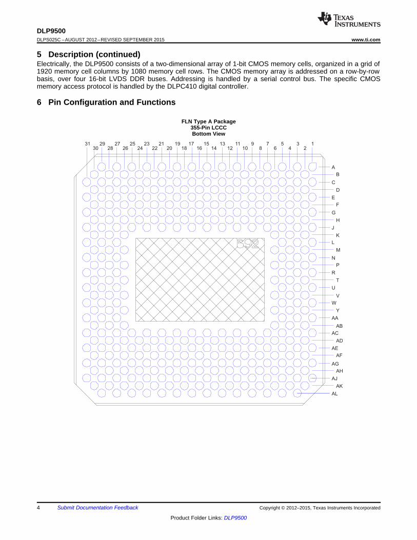
5 Description (continued)Electrically, the DLP9500 consists of a two-dimensional array of 1-bit CMOS memory cells, organized in a grid of1920 memory cell columns by 1080 memory cell rows. The CMOS memory array is addressed on a row-by-rowbasis, over four 16-bit LVDS DDR buses. Addressing is handled by a serial control bus. The specific CMOSmemory access protocol is handled by the DLPC410 digital controller.
6 Pin Configuration and Functions
FLN Type A Package355-Pin LCCCBottom View
4 Submit Documentation Feedback Copyright © 2012–2015, Texas Instruments Incorporated
Product Folder Links: DLP9500
DLP9500www.ti.com DLPS025C –AUGUST 2012–REVISED SEPTEMBER 2015
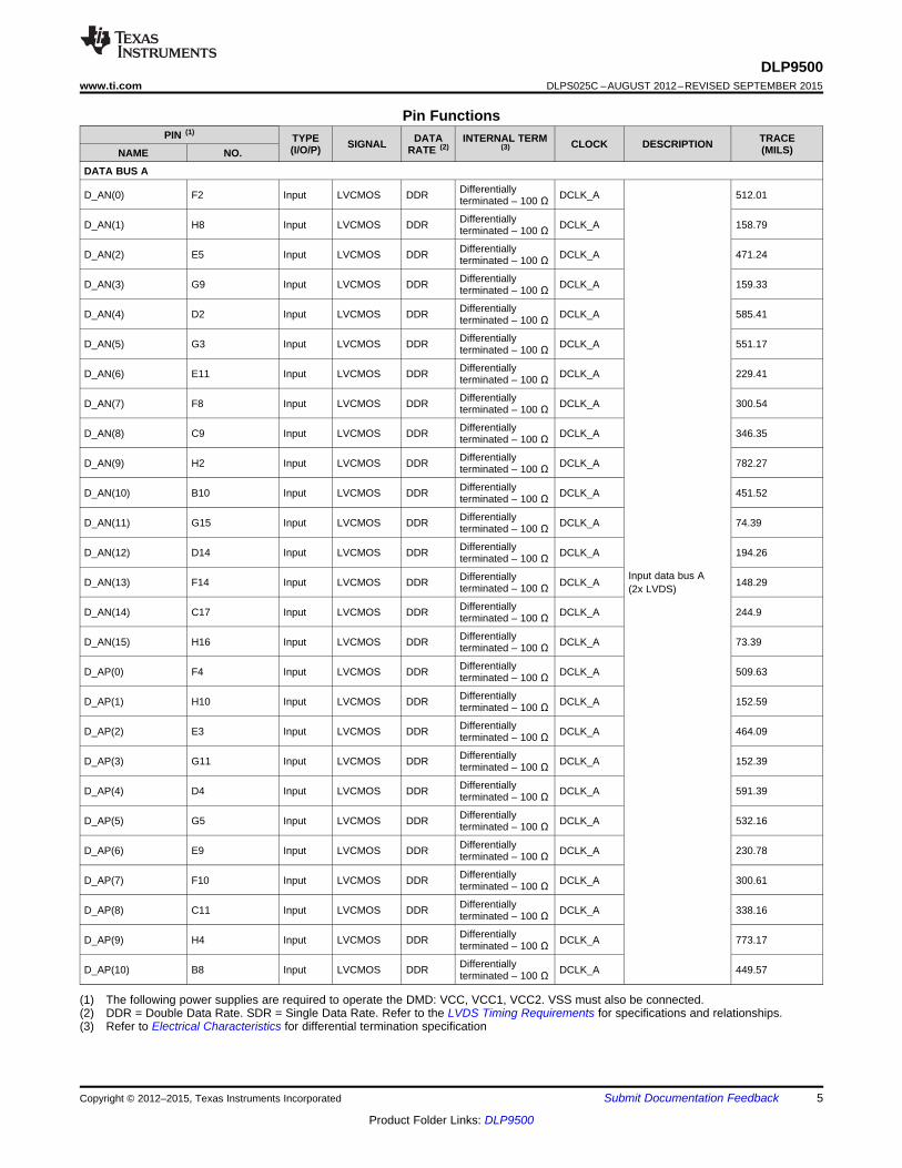
Pin FunctionsPIN (1)
TYPE DATA INTERNAL TERM TRACESIGNAL CLOCK DESCRIPTION(I/O/P) RATE (2) (3) (MILS)NAME NO.
DATA BUS A
DifferentiallyD_AN(0) F2 Input LVCMOS DDR DCLK_A 512.01terminated – 100 Ω
DifferentiallyD_AN(1) H8 Input LVCMOS DDR DCLK_A 158.79terminated – 100 Ω
DifferentiallyD_AN(2) E5 Input LVCMOS DDR DCLK_A 471.24terminated – 100 Ω
DifferentiallyD_AN(3) G9 Input LVCMOS DDR DCLK_A 159.33terminated – 100 Ω
DifferentiallyD_AN(4) D2 Input LVCMOS DDR DCLK_A 585.41terminated – 100 Ω
DifferentiallyD_AN(5) G3 Input LVCMOS DDR DCLK_A 551.17terminated – 100 Ω
DifferentiallyD_AN(6) E11 Input LVCMOS DDR DCLK_A 229.41terminated – 100 Ω
DifferentiallyD_AN(7) F8 Input LVCMOS DDR DCLK_A 300.54terminated – 100 Ω
DifferentiallyD_AN(8) C9 Input LVCMOS DDR DCLK_A 346.35terminated – 100 Ω
DifferentiallyD_AN(9) H2 Input LVCMOS DDR DCLK_A 782.27terminated – 100 Ω
DifferentiallyD_AN(10) B10 Input LVCMOS DDR DCLK_A 451.52terminated – 100 Ω
DifferentiallyD_AN(11) G15 Input LVCMOS DDR DCLK_A 74.39terminated – 100 Ω
DifferentiallyD_AN(12) D14 Input LVCMOS DDR DCLK_A 194.26terminated – 100 ΩInput data bus ADifferentiallyD_AN(13) F14 Input LVCMOS DDR DCLK_A 148.29terminated – 100 Ω (2x LVDS)
DifferentiallyD_AN(14) C17 Input LVCMOS DDR DCLK_A 244.9terminated – 100 Ω
DifferentiallyD_AN(15) H16 Input LVCMOS DDR DCLK_A 73.39terminated – 100 Ω
DifferentiallyD_AP(0) F4 Input LVCMOS DDR DCLK_A 509.63terminated – 100 Ω
DifferentiallyD_AP(1) H10 Input LVCMOS DDR DCLK_A 152.59terminated – 100 Ω
DifferentiallyD_AP(2) E3 Input LVCMOS DDR DCLK_A 464.09terminated – 100 Ω
DifferentiallyD_AP(3) G11 Input LVCMOS DDR DCLK_A 152.39terminated – 100 Ω
DifferentiallyD_AP(4) D4 Input LVCMOS DDR DCLK_A 591.39terminated – 100 Ω
DifferentiallyD_AP(5) G5 Input LVCMOS DDR DCLK_A 532.16terminated – 100 Ω
DifferentiallyD_AP(6) E9 Input LVCMOS DDR DCLK_A 230.78terminated – 100 Ω
DifferentiallyD_AP(7) F10 Input LVCMOS DDR DCLK_A 300.61terminated – 100 Ω
DifferentiallyD_AP(8) C11 Input LVCMOS DDR DCLK_A 338.16terminated – 100 Ω
DifferentiallyD_AP(9) H4 Input LVCMOS DDR DCLK_A 773.17terminated – 100 Ω
DifferentiallyD_AP(10) B8 Input LVCMOS DDR DCLK_A 449.57terminated – 100 Ω
(1) The following power supplies are required to operate the DMD: VCC, VCC1, VCC2. VSS must also be connected.(2) DDR = Double Data Rate. SDR = Single Data Rate. Refer to the LVDS Timing Requirements for specifications and relationships.(3) Refer to Electrical Characteristics for differential termination specification
Copyright © 2012–2015, Texas Instruments Incorporated Submit Documentation Feedback 5
Product Folder Links: DLP9500
DLP9500DLPS025C –AUGUST 2012–REVISED SEPTEMBER 2015 www.ti.com
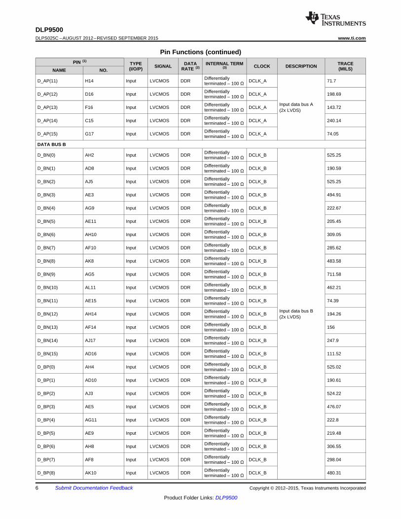
Pin Functions (continued)PIN (1)
TYPE DATA INTERNAL TERM TRACESIGNAL CLOCK DESCRIPTION(I/O/P) RATE (2) (3) (MILS)NAME NO.
DifferentiallyD_AP(11) H14 Input LVCMOS DDR DCLK_A 71.7terminated – 100 Ω
DifferentiallyD_AP(12) D16 Input LVCMOS DDR DCLK_A 198.69terminated – 100 ΩInput data bus ADifferentiallyD_AP(13) F16 Input LVCMOS DDR DCLK_A 143.72terminated – 100 Ω (2x LVDS)
DifferentiallyD_AP(14) C15 Input LVCMOS DDR DCLK_A 240.14terminated – 100 Ω
DifferentiallyD_AP(15) G17 Input LVCMOS DDR DCLK_A 74.05terminated – 100 Ω
DATA BUS B
DifferentiallyD_BN(0) AH2 Input LVCMOS DDR DCLK_B 525.25terminated – 100 Ω
DifferentiallyD_BN(1) AD8 Input LVCMOS DDR DCLK_B 190.59terminated – 100 Ω
DifferentiallyD_BN(2) AJ5 Input LVCMOS DDR DCLK_B 525.25terminated – 100 Ω
DifferentiallyD_BN(3) AE3 Input LVCMOS DDR DCLK_B 494.91terminated – 100 Ω
DifferentiallyD_BN(4) AG9 Input LVCMOS DDR DCLK_B 222.67terminated – 100 Ω
DifferentiallyD_BN(5) AE11 Input LVCMOS DDR DCLK_B 205.45terminated – 100 Ω
DifferentiallyD_BN(6) AH10 Input LVCMOS DDR DCLK_B 309.05terminated – 100 Ω
DifferentiallyD_BN(7) AF10 Input LVCMOS DDR DCLK_B 285.62terminated – 100 Ω
DifferentiallyD_BN(8) AK8 Input LVCMOS DDR DCLK_B 483.58terminated – 100 Ω
DifferentiallyD_BN(9) AG5 Input LVCMOS DDR DCLK_B 711.58terminated – 100 Ω
DifferentiallyD_BN(10) AL11 Input LVCMOS DDR DCLK_B 462.21terminated – 100 Ω
DifferentiallyD_BN(11) AE15 Input LVCMOS DDR DCLK_B 74.39terminated – 100 ΩInput data bus BDifferentiallyD_BN(12) AH14 Input LVCMOS DDR DCLK_B 194.26terminated – 100 Ω (2x LVDS)
DifferentiallyD_BN(13) AF14 Input LVCMOS DDR DCLK_B 156terminated – 100 Ω
DifferentiallyD_BN(14) AJ17 Input LVCMOS DDR DCLK_B 247.9terminated – 100 Ω
DifferentiallyD_BN(15) AD16 Input LVCMOS DDR DCLK_B 111.52terminated – 100 Ω
DifferentiallyD_BP(0) AH4 Input LVCMOS DDR DCLK_B 525.02terminated – 100 Ω
DifferentiallyD_BP(1) AD10 Input LVCMOS DDR DCLK_B 190.61terminated – 100 Ω
DifferentiallyD_BP(2) AJ3 Input LVCMOS DDR DCLK_B 524.22terminated – 100 Ω
DifferentiallyD_BP(3) AE5 Input LVCMOS DDR DCLK_B 476.07terminated – 100 Ω
DifferentiallyD_BP(4) AG11 Input LVCMOS DDR DCLK_B 222.8terminated – 100 Ω
DifferentiallyD_BP(5) AE9 Input LVCMOS DDR DCLK_B 219.48terminated – 100 Ω
DifferentiallyD_BP(6) AH8 Input LVCMOS DDR DCLK_B 306.55terminated – 100 Ω
DifferentiallyD_BP(7) AF8 Input LVCMOS DDR DCLK_B 298.04terminated – 100 Ω
DifferentiallyD_BP(8) AK10 Input LVCMOS DDR DCLK_B 480.31terminated – 100 Ω
6 Submit Documentation Feedback Copyright © 2012–2015, Texas Instruments Incorporated
Product Folder Links: DLP9500
DLP9500www.ti.com DLPS025C –AUGUST 2012–REVISED SEPTEMBER 2015
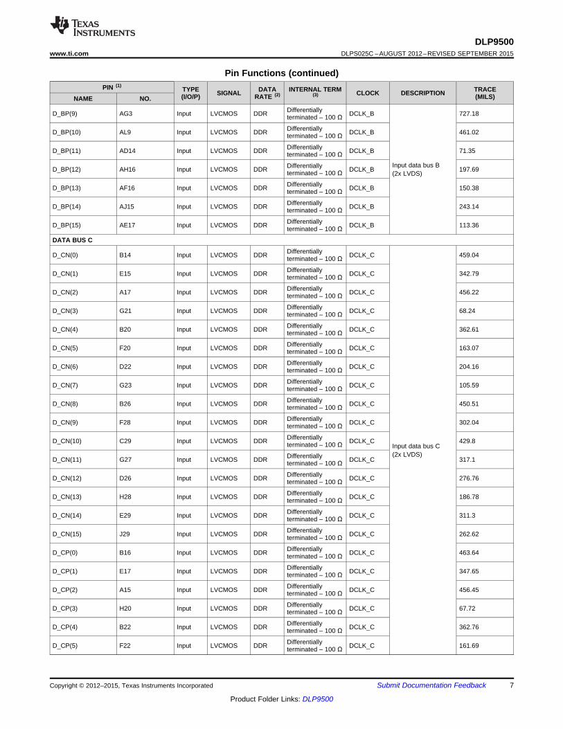
Pin Functions (continued)PIN (1)
TYPE DATA INTERNAL TERM TRACESIGNAL CLOCK DESCRIPTION(I/O/P) RATE (2) (3) (MILS)NAME NO.
DifferentiallyD_BP(9) AG3 Input LVCMOS DDR DCLK_B 727.18terminated – 100 Ω
DifferentiallyD_BP(10) AL9 Input LVCMOS DDR DCLK_B 461.02terminated – 100 Ω
DifferentiallyD_BP(11) AD14 Input LVCMOS DDR DCLK_B 71.35terminated – 100 ΩInput data bus BDifferentiallyD_BP(12) AH16 Input LVCMOS DDR DCLK_B 197.69terminated – 100 Ω (2x LVDS)
DifferentiallyD_BP(13) AF16 Input LVCMOS DDR DCLK_B 150.38terminated – 100 Ω
DifferentiallyD_BP(14) AJ15 Input LVCMOS DDR DCLK_B 243.14terminated – 100 Ω
DifferentiallyD_BP(15) AE17 Input LVCMOS DDR DCLK_B 113.36terminated – 100 Ω
DATA BUS C
DifferentiallyD_CN(0) B14 Input LVCMOS DDR DCLK_C 459.04terminated – 100 Ω
DifferentiallyD_CN(1) E15 Input LVCMOS DDR DCLK_C 342.79terminated – 100 Ω
DifferentiallyD_CN(2) A17 Input LVCMOS DDR DCLK_C 456.22terminated – 100 Ω
DifferentiallyD_CN(3) G21 Input LVCMOS DDR DCLK_C 68.24terminated – 100 Ω
DifferentiallyD_CN(4) B20 Input LVCMOS DDR DCLK_C 362.61terminated – 100 Ω
DifferentiallyD_CN(5) F20 Input LVCMOS DDR DCLK_C 163.07terminated – 100 Ω
DifferentiallyD_CN(6) D22 Input LVCMOS DDR DCLK_C 204.16terminated – 100 Ω
DifferentiallyD_CN(7) G23 Input LVCMOS DDR DCLK_C 105.59terminated – 100 Ω
DifferentiallyD_CN(8) B26 Input LVCMOS DDR DCLK_C 450.51terminated – 100 Ω
DifferentiallyD_CN(9) F28 Input LVCMOS DDR DCLK_C 302.04terminated – 100 Ω
DifferentiallyD_CN(10) C29 Input LVCMOS DDR DCLK_C 429.8terminated – 100 Ω Input data bus C(2x LVDS)DifferentiallyD_CN(11) G27 Input LVCMOS DDR DCLK_C 317.1terminated – 100 Ω
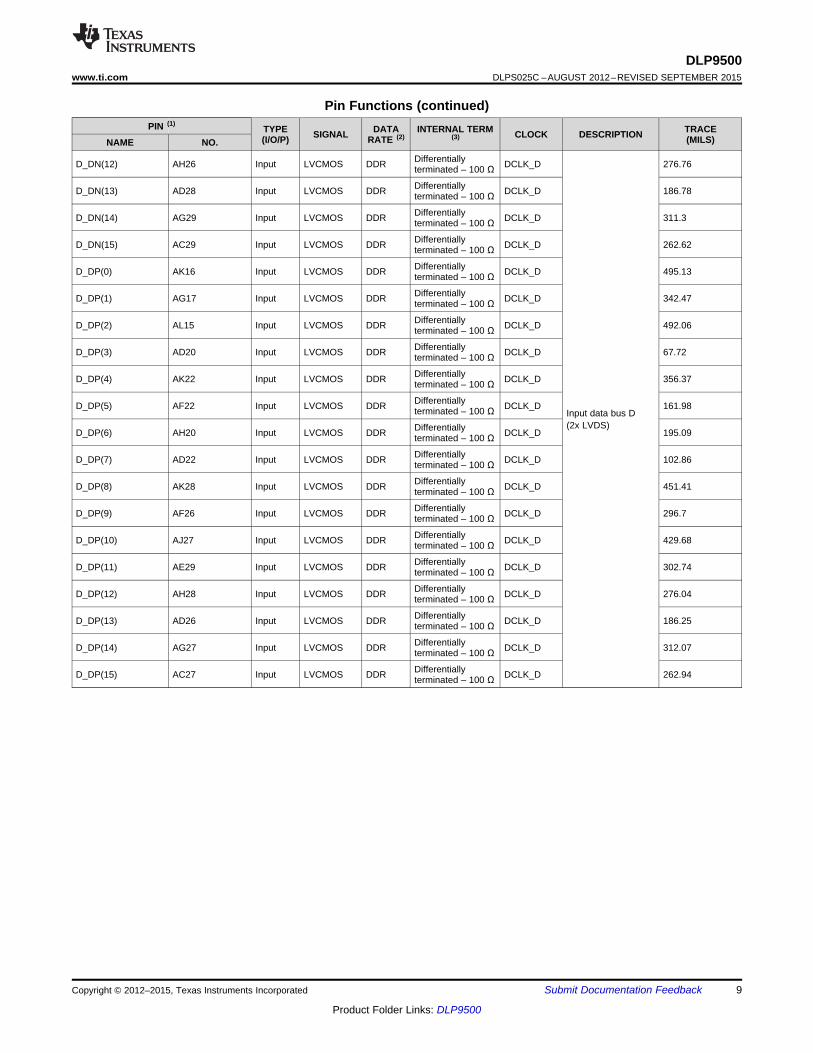
DifferentiallyD_CN(12) D26 Input LVCMOS DDR DCLK_C 276.76terminated – 100 Ω
DifferentiallyD_CN(13) H28 Input LVCMOS DDR DCLK_C 186.78terminated – 100 Ω
DifferentiallyD_CN(14) E29 Input LVCMOS DDR DCLK_C 311.3terminated – 100 Ω
DifferentiallyD_CN(15) J29 Input LVCMOS DDR DCLK_C 262.62terminated – 100 Ω
DifferentiallyD_CP(0) B16 Input LVCMOS DDR DCLK_C 463.64terminated – 100 Ω
DifferentiallyD_CP(1) E17 Input LVCMOS DDR DCLK_C 347.65terminated – 100 Ω
DifferentiallyD_CP(2) A15 Input LVCMOS DDR DCLK_C 456.45terminated – 100 Ω
DifferentiallyD_CP(3) H20 Input LVCMOS DDR DCLK_C 67.72terminated – 100 Ω
DifferentiallyD_CP(4) B22 Input LVCMOS DDR DCLK_C 362.76terminated – 100 Ω
DifferentiallyD_CP(5) F22 Input LVCMOS DDR DCLK_C 161.69terminated – 100 Ω
Copyright © 2012–2015, Texas Instruments Incorporated Submit Documentation Feedback 7
Product Folder Links: DLP9500
DLP9500DLPS025C –AUGUST 2012–REVISED SEPTEMBER 2015 www.ti.com
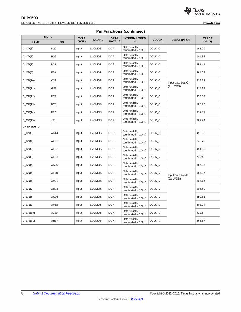
Pin Functions (continued)PIN (1)
TYPE DATA INTERNAL TERM TRACESIGNAL CLOCK DESCRIPTION(I/O/P) RATE (2) (3) (MILS)NAME NO.
DifferentiallyD_CP(6) D20 Input LVCMOS DDR DCLK_C 195.09terminated – 100 Ω
DifferentiallyD_CP(7) H22 Input LVCMOS DDR DCLK_C 104.86terminated – 100 Ω
DifferentiallyD_CP(8) B28 Input LVCMOS DDR DCLK_C 451.41terminated – 100 Ω
DifferentiallyD_CP(9) F26 Input LVCMOS DDR DCLK_C 294.22terminated – 100 Ω
DifferentiallyD_CP(10) C27 Input LVCMOS DDR DCLK_C 429.68terminated – 100 Ω Input data bus C(2x LVDS)DifferentiallyD_CP(11) G29 Input LVCMOS DDR DCLK_C 314.98terminated – 100 Ω
DifferentiallyD_CP(12) D28 Input LVCMOS DDR DCLK_C 276.04terminated – 100 Ω
DifferentiallyD_CP(13) H26 Input LVCMOS DDR DCLK_C 186.25terminated – 100 Ω
DifferentiallyD_CP(14) E27 Input LVCMOS DDR DCLK_C 312.07terminated – 100 Ω
DifferentiallyD_CP(15) J27 Input LVCMOS DDR DCLK_C 262.94terminated – 100 Ω
DATA BUS D
DifferentiallyD_DN(0) AK14 Input LVCMOS DDR DCLK_D 492.53terminated – 100 Ω
DifferentiallyD_DN(1) AG15 Input LVCMOS DDR DCLK_D 342.78terminated – 100 Ω
DifferentiallyD_DN(2) AL17 Input LVCMOS DDR DCLK_D 491.83terminated – 100 Ω
DifferentiallyD_DN(3) AE21 Input LVCMOS DDR DCLK_D 74.24terminated – 100 Ω
DifferentiallyD_DN(4) AK20 Input LVCMOS DDR DCLK_D 356.23terminated – 100 Ω
DifferentiallyD_DN(5) AF20 Input LVCMOS DDR DCLK_D 163.07terminated – 100 Ω Input data bus D(2x LVDS)DifferentiallyD_DN(6) AH22 Input LVCMOS DDR DCLK_D 204.16terminated – 100 Ω
DifferentiallyD_DN(7) AE23 Input LVCMOS DDR DCLK_D 105.59terminated – 100 Ω
DifferentiallyD_DN(8) AK26 Input LVCMOS DDR DCLK_D 450.51terminated – 100 Ω
DifferentiallyD_DN(9) AF28 Input LVCMOS DDR DCLK_D 302.04terminated – 100 Ω
DifferentiallyD_DN(10) AJ29 Input LVCMOS DDR DCLK_D 429.8terminated – 100 Ω
DifferentiallyD_DN(11) AE27 Input LVCMOS DDR DCLK_D 298.87terminated – 100 Ω
8 Submit Documentation Feedback Copyright © 2012–2015, Texas Instruments Incorporated
Product Folder Links: DLP9500
DLP9500www.ti.com DLPS025C –AUGUST 2012–REVISED SEPTEMBER 2015
Pin Functions (continued)PIN (1)
TYPE DATA INTERNAL TERM TRACESIGNAL CLOCK DESCRIPTION(I/O/P) RATE (2) (3) (MILS)NAME NO.
DifferentiallyD_DN(12) AH26 Input LVCMOS DDR DCLK_D 276.76terminated – 100 Ω
DifferentiallyD_DN(13) AD28 Input LVCMOS DDR DCLK_D 186.78terminated – 100 Ω
DifferentiallyD_DN(14) AG29 Input LVCMOS DDR DCLK_D 311.3terminated – 100 Ω
DifferentiallyD_DN(15) AC29 Input LVCMOS DDR DCLK_D 262.62terminated – 100 Ω
DifferentiallyD_DP(0) AK16 Input LVCMOS DDR DCLK_D 495.13terminated – 100 Ω
DifferentiallyD_DP(1) AG17 Input LVCMOS DDR DCLK_D 342.47terminated – 100 Ω
DifferentiallyD_DP(2) AL15 Input LVCMOS DDR DCLK_D 492.06terminated – 100 Ω
DifferentiallyD_DP(3) AD20 Input LVCMOS DDR DCLK_D 67.72terminated – 100 Ω
DifferentiallyD_DP(4) AK22 Input LVCMOS DDR DCLK_D 356.37terminated – 100 Ω
DifferentiallyD_DP(5) AF22 Input LVCMOS DDR DCLK_D 161.98terminated – 100 Ω Input data bus D(2x LVDS)DifferentiallyD_DP(6) AH20 Input LVCMOS DDR DCLK_D 195.09terminated – 100 Ω
DifferentiallyD_DP(7) AD22 Input LVCMOS DDR DCLK_D 102.86terminated – 100 Ω
DifferentiallyD_DP(8) AK28 Input LVCMOS DDR DCLK_D 451.41terminated – 100 Ω
DifferentiallyD_DP(9) AF26 Input LVCMOS DDR DCLK_D 296.7terminated – 100 Ω
DifferentiallyD_DP(10) AJ27 Input LVCMOS DDR DCLK_D 429.68terminated – 100 Ω
DifferentiallyD_DP(11) AE29 Input LVCMOS DDR DCLK_D 302.74terminated – 100 Ω
DifferentiallyD_DP(12) AH28 Input LVCMOS DDR DCLK_D 276.04terminated – 100 Ω
DifferentiallyD_DP(13) AD26 Input LVCMOS DDR DCLK_D 186.25terminated – 100 Ω
DifferentiallyD_DP(14) AG27 Input LVCMOS DDR DCLK_D 312.07terminated – 100 Ω
DifferentiallyD_DP(15) AC27 Input LVCMOS DDR DCLK_D 262.94terminated – 100 Ω
Copyright © 2012–2015, Texas Instruments Incorporated Submit Documentation Feedback 9
Product Folder Links: DLP9500
DLP9500DLPS025C –AUGUST 2012–REVISED SEPTEMBER 2015 www.ti.com
Pin Functions (continued)PIN (1)
TYPE DATA INTERNAL TERM TRACESIGNAL CLOCK DESCRIPTION(I/O/P) RATE (2) (3) (MILS)NAME NO.
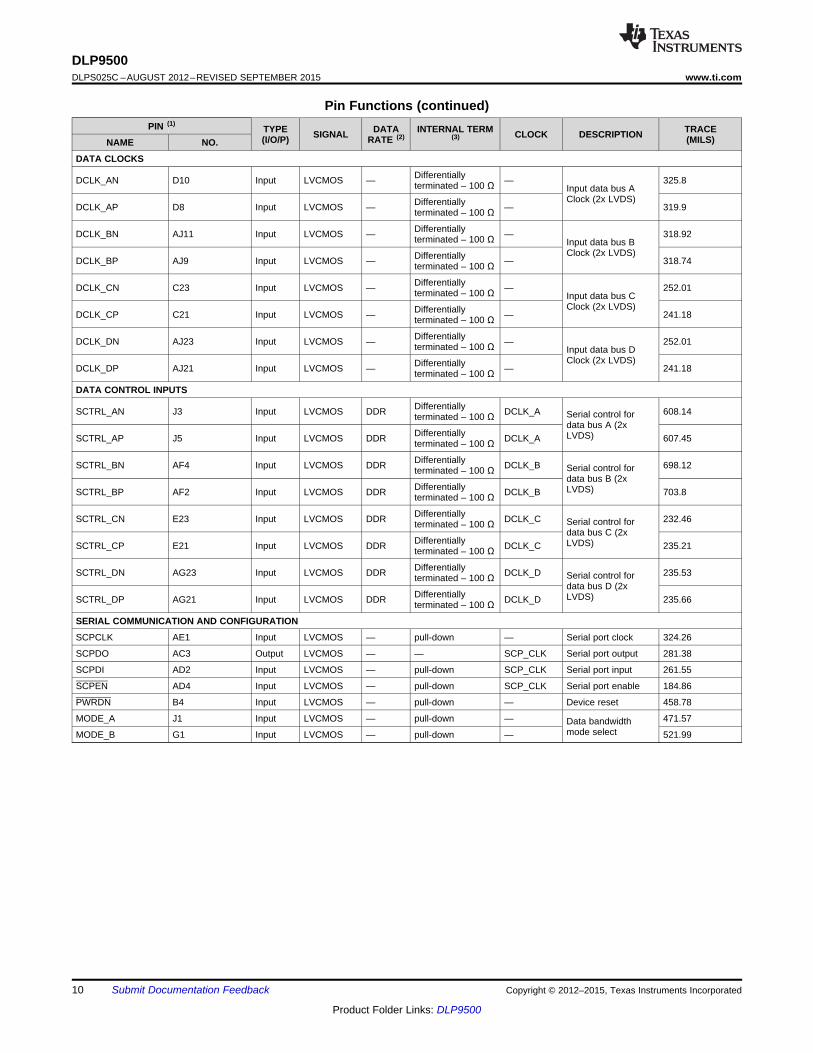
DATA CLOCKS
DifferentiallyDCLK_AN D10 Input LVCMOS — — 325.8terminated – 100 Ω Input data bus AClock (2x LVDS)DifferentiallyDCLK_AP D8 Input LVCMOS — — 319.9terminated – 100 Ω
DifferentiallyDCLK_BN AJ11 Input LVCMOS — — 318.92terminated – 100 Ω Input data bus BClock (2x LVDS)DifferentiallyDCLK_BP AJ9 Input LVCMOS — — 318.74terminated – 100 Ω
DifferentiallyDCLK_CN C23 Input LVCMOS — — 252.01terminated – 100 Ω Input data bus CClock (2x LVDS)DifferentiallyDCLK_CP C21 Input LVCMOS — — 241.18terminated – 100 Ω
DifferentiallyDCLK_DN AJ23 Input LVCMOS — — 252.01terminated – 100 Ω Input data bus DClock (2x LVDS)DifferentiallyDCLK_DP AJ21 Input LVCMOS — — 241.18terminated – 100 Ω
DATA CONTROL INPUTS
DifferentiallySCTRL_AN J3 Input LVCMOS DDR DCLK_A 608.14Serial control forterminated – 100 Ωdata bus A (2x
Differentially LVDS)SCTRL_AP J5 Input LVCMOS DDR DCLK_A 607.45terminated – 100 Ω
DifferentiallySCTRL_BN AF4 Input LVCMOS DDR DCLK_B 698.12Serial control forterminated – 100 Ωdata bus B (2x
Differentially LVDS)SCTRL_BP AF2 Input LVCMOS DDR DCLK_B 703.8terminated – 100 Ω
DifferentiallySCTRL_CN E23 Input LVCMOS DDR DCLK_C 232.46Serial control forterminated – 100 Ωdata bus C (2x
Differentially LVDS)SCTRL_CP E21 Input LVCMOS DDR DCLK_C 235.21terminated – 100 Ω
DifferentiallySCTRL_DN AG23 Input LVCMOS DDR DCLK_D 235.53Serial control forterminated – 100 Ωdata bus D (2x
Differentially LVDS)SCTRL_DP AG21 Input LVCMOS DDR DCLK_D 235.66terminated – 100 Ω
SERIAL COMMUNICATION AND CONFIGURATION
SCPCLK AE1 Input LVCMOS — pull-down — Serial port clock 324.26
SCPDO AC3 Output LVCMOS — — SCP_CLK Serial port output 281.38
SCPDI AD2 Input LVCMOS — pull-down SCP_CLK Serial port input 261.55
SCPEN AD4 Input LVCMOS — pull-down SCP_CLK Serial port enable 184.86
PWRDN B4 Input LVCMOS — pull-down — Device reset 458.78
MODE_A J1 Input LVCMOS — pull-down — 471.57Data bandwidthmode selectMODE_B G1 Input LVCMOS — pull-down — 521.99
10 Submit Documentation Feedback Copyright © 2012–2015, Texas Instruments Incorporated
Product Folder Links: DLP9500
DLP9500www.ti.com DLPS025C –AUGUST 2012–REVISED SEPTEMBER 2015
Pin Functions (continued)PIN (1)
TYPE DATA INTERNAL TERM TRACESIGNAL CLOCK DESCRIPTION(I/O/P) RATE (2) (3) (MILS)NAME NO.
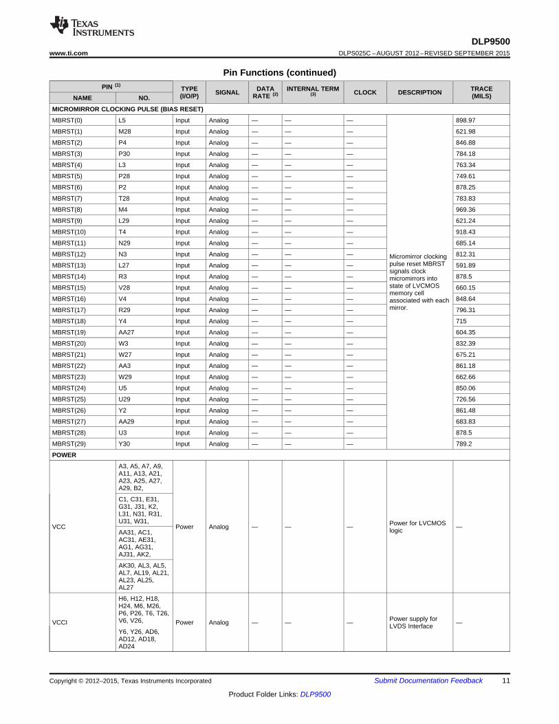
MICROMIRROR CLOCKING PULSE (BIAS RESET)
MBRST(0) L5 Input Analog — — — 898.97
MBRST(1) M28 Input Analog — — — 621.98
MBRST(2) P4 Input Analog — — — 846.88
MBRST(3) P30 Input Analog — — — 784.18
MBRST(4) L3 Input Analog — — — 763.34
MBRST(5) P28 Input Analog — — — 749.61
MBRST(6) P2 Input Analog — — — 878.25
MBRST(7) T28 Input Analog — — — 783.83
MBRST(8) M4 Input Analog — — — 969.36
MBRST(9) L29 Input Analog — — — 621.24
MBRST(10) T4 Input Analog — — — 918.43
MBRST(11) N29 Input Analog — — — 685.14
MBRST(12) N3 Input Analog — — — 812.31Micromirror clockingpulse reset MBRSTMBRST(13) L27 Input Analog — — — 591.89signals clock
MBRST(14) R3 Input Analog — — — 878.5micromirrors intostate of LVCMOSMBRST(15) V28 Input Analog — — — 660.15memory cell
MBRST(16) V4 Input Analog — — — 848.64associated with eachmirror.MBRST(17) R29 Input Analog — — — 796.31
MBRST(18) Y4 Input Analog — — — 715
MBRST(19) AA27 Input Analog — — — 604.35
MBRST(20) W3 Input Analog — — — 832.39
MBRST(21) W27 Input Analog — — — 675.21
MBRST(22) AA3 Input Analog — — — 861.18
MBRST(23) W29 Input Analog — — — 662.66
MBRST(24) U5 Input Analog — — — 850.06
MBRST(25) U29 Input Analog — — — 726.56
MBRST(26) Y2 Input Analog — — — 861.48
MBRST(27) AA29 Input Analog — — — 683.83
MBRST(28) U3 Input Analog — — — 878.5
MBRST(29) Y30 Input Analog — — — 789.2
POWER
A3, A5, A7, A9,A11, A13, A21,A23, A25, A27,A29, B2,
C1, C31, E31,G31, J31, K2,L31, N31, R31,U31, W31, Power for LVCMOSVCC Power Analog — — — —logicAA31, AC1,AC31, AE31,AG1, AG31,AJ31, AK2,
AK30, AL3, AL5,AL7, AL19, AL21,AL23, AL25,AL27
H6, H12, H18,H24, M6, M26,P6, P26, T6, T26,
Power supply forV6, V26,VCCI Power Analog — — — —LVDS InterfaceY6, Y26, AD6,AD12, AD18,AD24
Copyright © 2012–2015, Texas Instruments Incorporated Submit Documentation Feedback 11
Product Folder Links: DLP9500
DLP9500DLPS025C –AUGUST 2012–REVISED SEPTEMBER 2015 www.ti.com
Pin Functions (continued)PIN (1)
TYPE DATA INTERNAL TERM TRACESIGNAL CLOCK DESCRIPTION(I/O/P) RATE (2) (3) (MILS)NAME NO.
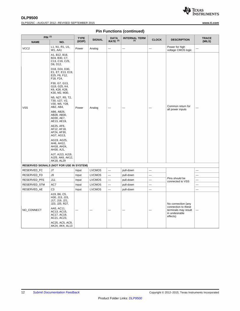
L1, N1, R1, U1, Power for highVCC2 Power Analog — — — —W1, AA1 voltage CMOS logic
A1, B12, B18,B24, B30, C7,C13, C19, C25,D6, D12,
D18, D24, D30,E1, E7, E13, E19,E25, F6, F12,F18, F24,
F30, G7, G13,G19, G25, K4,K6, K26, K28,K30, M2, M30,
N5, N27, R5, T2,T30, U27, V2,V30, W5, Y28,
Common return forAB2, AB4,VSS Power Analog — — — —all power inputsAB6, AB26,AB28, AB30,AD30, AE7,AE13, AE19,
AE25, AF6,AF12, AF18,AF24, AF30,AG7, AG13,
AG19, AG25,AH6, AH12,AH18, AH24,AH30, AJ1,
AJ7, AJ13, AJ19,AJ25, AK6, AK12,AK18, AL29
RESERVED SIGNALS (NOT FOR USE IN SYSTEM)
RESERVED_FC J7 Input LVCMOS — pull-down — —
RESERVED_FD J9 Input LVCMOS — pull-down — —Pins should beRESERVED_PFE J11 Input LVCMOS — pull-down — —connected to VSS
RESERVED_STM AC7 Input LVCMOS — pull-down — —
RESERVED_AE C3 Input LVCMOS — pull-down — —
A19, B6, C5,H30, J13, J15,J17, J19, J21,J23, J25, R27, No connection (any
connection to theseAA5, AC11,NO_CONNECT — — — — — terminals may result —AC13, AC15, in undesirableAC17, AC19, effects)AC21, AC23,
AC25, AC5, AC9,AK24, AK4, AL13
12 Submit Documentation Feedback Copyright © 2012–2015, Texas Instruments Incorporated
Product Folder Links: DLP9500
DLP9500www.ti.com DLPS025C –AUGUST 2012–REVISED SEPTEMBER 2015
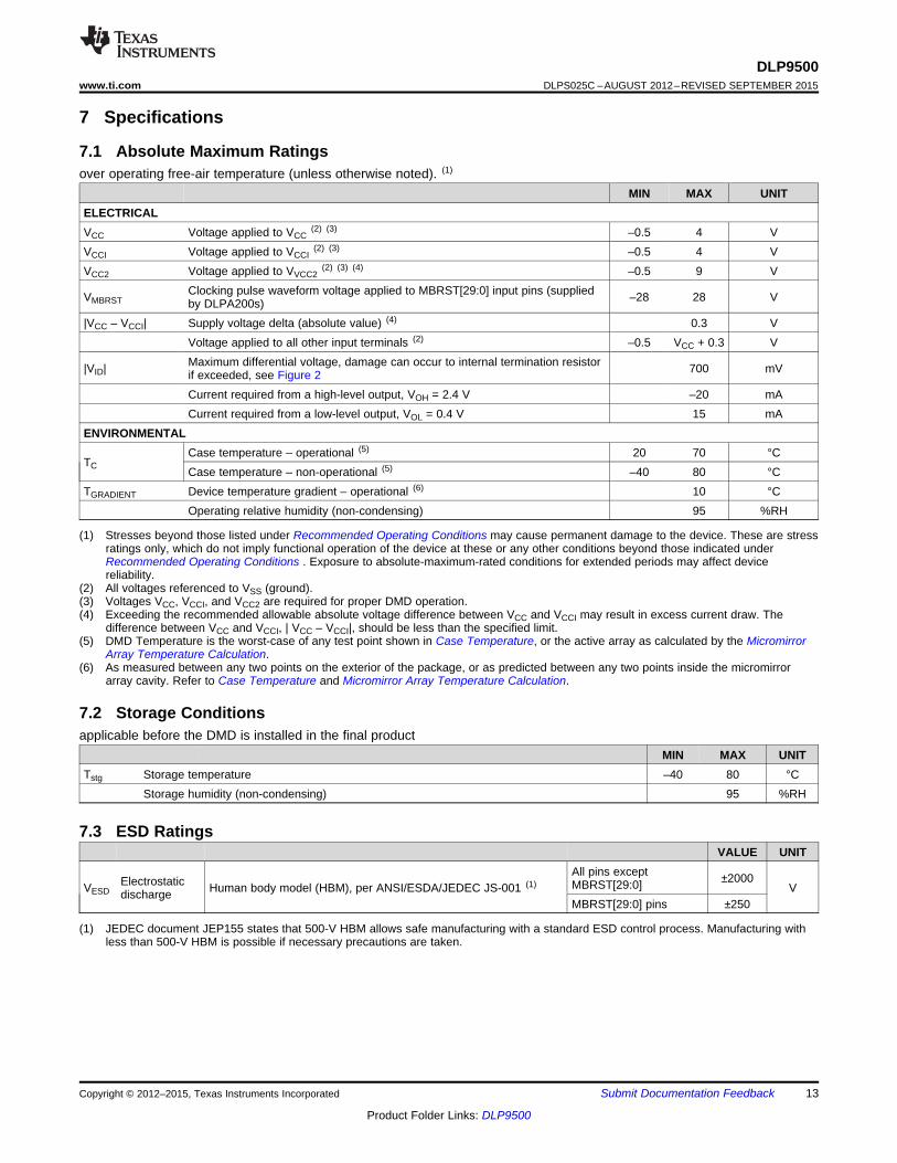
7 Specifications
7.1 Absolute Maximum Ratingsover operating free-air temperature (unless otherwise noted). (1)
MIN MAX UNITELECTRICALVCC Voltage applied to VCC
(2) (3) –0.5 4 VVCCI Voltage applied to VCCI
(2) (3) –0.5 4 VVCC2 Voltage applied to VVCC2
(2) (3) (4) –0.5 9 VClocking pulse waveform voltage applied to MBRST[29:0] input pins (suppliedVMBRST –28 28 Vby DLPA200s)
|VCC – VCCI| Supply voltage delta (absolute value) (4) 0.3 VVoltage applied to all other input terminals (2) –0.5 VCC + 0.3 VMaximum differential voltage, damage can occur to internal termination resistor|VID| 700 mVif exceeded, see Figure 2Current required from a high-level output, VOH = 2.4 V –20 mACurrent required from a low-level output, VOL = 0.4 V 15 mA
ENVIRONMENTALCase temperature – operational (5) 20 70 °C
TC Case temperature – non-operational (5) –40 80 °CTGRADIENT Device temperature gradient – operational (6) 10 °C
Operating relative humidity (non-condensing) 95 %RH
(1) Stresses beyond those listed under Recommended Operating Conditions may cause permanent damage to the device. These are stressratings only, which do not imply functional operation of the device at these or any other conditions beyond those indicated underRecommended Operating Conditions . Exposure to absolute-maximum-rated conditions for extended periods may affect devicereliability.
(2) All voltages referenced to VSS (ground).(3) Voltages VCC, VCCI, and VCC2 are required for proper DMD operation.(4) Exceeding the recommended allowable absolute voltage difference between VCC and VCCI may result in excess current draw. The
difference between VCC and VCCI, | VCC – VCCI|, should be less than the specified limit.(5) DMD Temperature is the worst-case of any test point shown in Case Temperature, or the active array as calculated by the Micromirror
Array Temperature Calculation.(6) As measured between any two points on the exterior of the package, or as predicted between any two points inside the micromirror
array cavity. Refer to Case Temperature and Micromirror Array Temperature Calculation.
7.2 Storage Conditionsapplicable before the DMD is installed in the final product
MIN MAX UNITTstg Storage temperature –40 80 °C
Storage humidity (non-condensing) 95 %RH
7.3 ESD RatingsVALUE UNIT
All pins except ±2000Electrostatic MBRST[29:0]VESD Human body model (HBM), per ANSI/ESDA/JEDEC JS-001 (1) VdischargeMBRST[29:0] pins ±250
(1) JEDEC document JEP155 states that 500-V HBM allows safe manufacturing with a standard ESD control process. Manufacturing withless than 500-V HBM is possible if necessary precautions are taken.
Copyright © 2012–2015, Texas Instruments Incorporated Submit Documentation Feedback 13
Product Folder Links: DLP9500
DLP9500DLPS025C –AUGUST 2012–REVISED SEPTEMBER 2015 www.ti.com
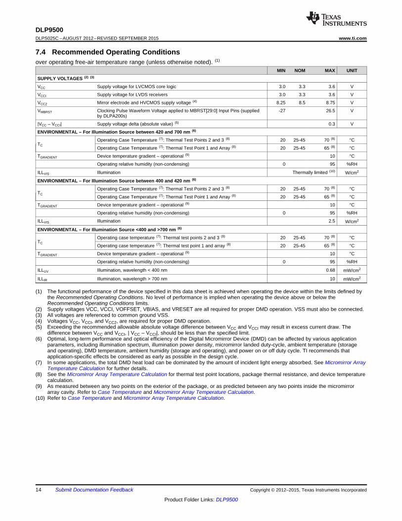
7.4 Recommended Operating Conditionsover operating free-air temperature range (unless otherwise noted). (1)
MIN NOM MAX UNIT
SUPPLY VOLTAGES (2) (3)
VCC Supply voltage for LVCMOS core logic 3.0 3.3 3.6 V
VCCI Supply voltage for LVDS receivers 3.0 3.3 3.6 V
VCC2 Mirror electrode and HVCMOS supply voltage (4) 8.25 8.5 8.75 V
VMBRST Clocking Pulse Waveform Voltage applied to MBRST[29:0] Input Pins (supplied -27 26.5 Vby DLPA200s)
|VCC – VCCI| Supply voltage delta (absolute value) (5) 0.3 V
ENVIRONMENTAL – For Illumination Source between 420 and 700 nm (6)
Operating Case Temperature (7): Thermal Test Points 2 and 3 (8) 20 25-45 70 (8) °CTC
Operating Case Temperature (7): Thermal Test Point 1 and Array (8) 20 25-45 65 (8) °C
TGRADIENT Device temperature gradient – operational (9) 10 °C
Operating relative humidity (non-condensing) 0 95 %RH
ILLVIS Illumination Thermally limited (10) W/cm2
ENVIRONMENTAL – For Illumination Source between 400 and 420 nm (6)
Operating Case Temperature (7): Thermal Test Points 2 and 3 (8) 20 25-45 70 (8) °CTC
Operating Case Temperature (7): Thermal Test Point 1 and Array (8) 20 25-45 65 (8) °C
TGRADIENT Device temperature gradient – operational (9) 10 °C
Operating relative humidity (non-condensing) 0 95 %RH
ILLVIS Illumination 2.5 W/cm2
ENVIRONMENTAL – For Illumination Source <400 and >700 nm (6)
Operating case temperature (7): Thermal test points 2 and 3 (8) 20 25-45 70 (8) °CTC
Operating case temperature (7): Thermal test point 1 and array (8) 20 25-45 65 (8) °C
TGRADIENT Device temperature gradient – operational (9) 10 °C
Operating relative humidity (non-condensing) 0 95 %RH
ILLUV Illumination, wavelength < 400 nm 0.68 mW/cm2
ILLIR Illumination, wavelength > 700 nm 10 mW/cm2
(1) The functional performance of the device specified in this data sheet is achieved when operating the device within the limits defined bythe Recommended Operating Conditions. No level of performance is implied when operating the device above or below theRecommended Operating Conditions limits.
(2) Supply voltages VCC, VCCI, VOFFSET, VBIAS, and VRESET are all required for proper DMD operation. VSS must also be connected.(3) All voltages are referenced to common ground VSS.(4) Voltages VCC, VCCI, and VCC2, are required for proper DMD operation.(5) Exceeding the recommended allowable absolute voltage difference between VCC and VCCI may result in excess current draw. The
difference between VCC and VCCI, | VCC – VCCI|, should be less than the specified limit.(6) Optimal, long-term performance and optical efficiency of the Digital Micromirror Device (DMD) can be affected by various application
parameters, including illumination spectrum, illumination power density, micromirror landed duty-cycle, ambient temperature (storageand operating), DMD temperature, ambient humidity (storage and operating), and power on or off duty cycle. TI recommends thatapplication-specific effects be considered as early as possible in the design cycle.
(7) In some applications, the total DMD heat load can be dominated by the amount of incident light energy absorbed. See Micromirror ArrayTemperature Calculation for further details.
(8) See the Micromirror Array Temperature Calculation for thermal test point locations, package thermal resistance, and device temperaturecalculation.
(9) As measured between any two points on the exterior of the package, or as predicted between any two points inside the micromirrorarray cavity. Refer to Case Temperature and Micromirror Array Temperature Calculation.
(10) Refer to Case Temperature and Micromirror Array Temperature Calculation.
14 Submit Documentation Feedback Copyright © 2012–2015, Texas Instruments Incorporated
Product Folder Links: DLP9500
DLP9500www.ti.com DLPS025C –AUGUST 2012–REVISED SEPTEMBER 2015
7.5 Thermal InformationDLP9500
THERMAL METRIC (1) (2) LCCC UNIT355 PINS
Active micromirror array resistance to TC2 0.5 °C/W
(1) The DMD is designed to conduct absorbed and dissipated heat to the back of the package where it can be removed by an appropriateheat sink. The heat sink and cooling system must be capable of maintaining the package within the temperature range specified in theRecommended Operating Conditions. The total heat load on the DMD is largely driven by the incident light absorbed by the active area;although other contributions include light energy absorbed by the window aperture and electrical power dissipation of the array. Opticalsystems should be designed to minimize the light energy falling outside the window clear aperture since any additional thermal load inthis area can significantly degrade the reliability of the device.
(2) For more information about traditional and new thermal metrics, see the Semiconductor and IC Package Thermal Metrics applicationreport, SPRA953.
7.6 Electrical Characteristicsover the range of recommended supply voltage and recommended case operating temperature (unless otherwise noted);under recommended operating conditions
PARAMETER TEST CONDITIONS MIN TYP MAX UNITHigh-level output voltage (1),VOH VCC = 3 V, IOH = –20 mA 2.4 VSee Figure 11Low-level output voltage (1),VOL VCC = 3.6 V, IOH = 15 mA 0.4 VSee Figure 11Clocking pulse waveform applied to
VMBRST MBRST[29:0] input pins (supplied by –27 26.5 VDLPA200s)
IOZ High-impedance output current (1) VCC = 3.6 V 10 µAVOH = 2.4 V, VCC ≥ 3 V –20
IOH High-level output current (1) mAVOH = 1.7 V, VCC ≥ 2.25 V –15
IOL VOL = 0.4 V, VCC ≥ 3 V 15Low-level output current (1) mA
VOL = 0.4 V, VCC ≥ 2.25 V 14VIH High-level input voltage (1) 1.7 VCC + .3 VVIL Low-level input voltage (1) –0.3 0.7 VIIL Low-level input current (1) VCC = 3.6 V, VI = 0 V –60 µAIIH High-level input current (1) VCC = 3.6 V, VI = VCC 60 µAICC Current into VCC pin VCC = 3.6 V, 2990 mAICCI Current into VOFFSET pin (2) VCCI = 3.6 V 910 mAICC2 Current into VCC2 pin VCC2 = 8.75 V 25 mAPD Power dissipation 4.4 WZIN Internal differential impedance 95 105 ΩZLINE Line differential impedance (PWB, trace) 90 100 110 ΩCI Input capacitance (1) ƒ = 1 MHz 10 pFCO Output capacitance (1) ƒ = 1 MHz 10 pFCIM Input capacitance for MBRST[29:0] pins ƒ = 1 MHz 270 355 pF
(1) Applies to LVCMOS pins only.(2) Exceeding the maximum allowable absolute voltage difference between VCC and VCCI may result in excess current draw. (See Absolute
Maximum Ratings for details.)
Copyright © 2012–2015, Texas Instruments Incorporated Submit Documentation Feedback 15
Product Folder Links: DLP9500
SCTRL_AN
SCTRL_AP
D_AN(15:0)
D_AP(15:0)
D_BN(15:0)D_BP(15:0)
DCLK_BN
DCLK_BP
SCTRL_BNSCTRL_BP
DCLK_AN
DCLK_APt w
tc
th
th
ts
ts
t ske
w
SCTRL_CNSCTRL_CP
D_CN(15:0)D_CP(15:0)
D_DN(15:0)
D_DP(15:0)
DCLK_DNDCLK_DP
SCTRL_DNSCTRL_DP
DCLK_CNDCLK_CP
t ske
w
t w
ts
ts
th
th
t w
tc
t w
ts
tsth
tht w tc
t w
ts
tsth
tht w tc
t w
DLP9500DLPS025C –AUGUST 2012–REVISED SEPTEMBER 2015 www.ti.com
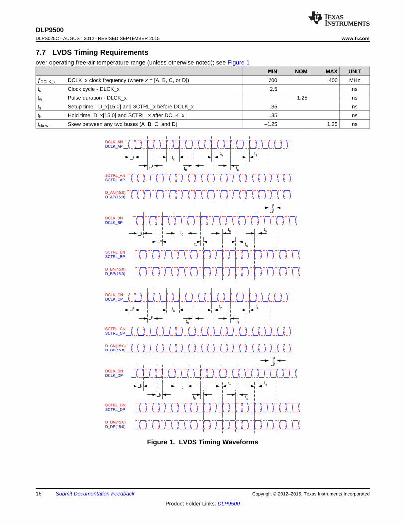
7.7 LVDS Timing Requirementsover operating free-air temperature range (unless otherwise noted); see Figure 1
MIN NOM MAX UNITƒDCLK_x DCLK_x clock frequency (where x = [A, B, C, or D]) 200 400 MHztc Clock cycle - DLCK_x 2.5 nstw Pulse duration - DLCK_x 1.25 nsts Setup time - D_x[15:0] and SCTRL_x before DCLK_x .35 nsth Hold time, D_x[15:0] and SCTRL_x after DCLK_x .35 nstskew Skew between any two buses (A ,B, C, and D) –1.25 1.25 ns
Figure 1. LVDS Timing Waveforms
16 Submit Documentation Feedback Copyright © 2012–2015, Texas Instruments Incorporated
Product Folder Links: DLP9500
VCM
VID
t r
tf
VLVDS max
= VCM max
+ | 1/2 × VID max
VLVDS min
= VCM min
± | 1/2 × VID max
|
|
DLP9500www.ti.com DLPS025C –AUGUST 2012–REVISED SEPTEMBER 2015
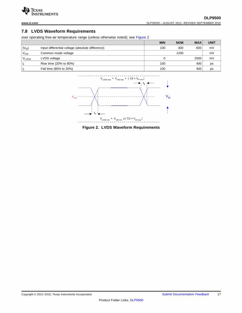
7.8 LVDS Waveform Requirementsover operating free-air temperature range (unless otherwise noted); see Figure 2
MIN NOM MAX UNIT|VID| Input differential voltage (absolute difference) 100 400 600 mVVCM Common mode voltage 1200 mVVLVDS LVDS voltage 0 2000 mVtr Rise time (20% to 80%) 100 400 pstr Fall time (80% to 20%) 100 400 ps
Figure 2. LVDS Waveform Requirements
Copyright © 2012–2015, Texas Instruments Incorporated Submit Documentation Feedback 17
Product Folder Links: DLP9500
V /2CC
0 v
SCP_CLK,
SCP_DI,
SCP_EN
Input Controller VCC
tr_SCP
tf_SCP
50% 50%
tc fclock = 1 / tc
SCPCLK
SCPDI 50%
tSCP_SKEW
SCPD0 50%
tSCP_DELAY
DLP9500DLPS025C –AUGUST 2012–REVISED SEPTEMBER 2015 www.ti.com
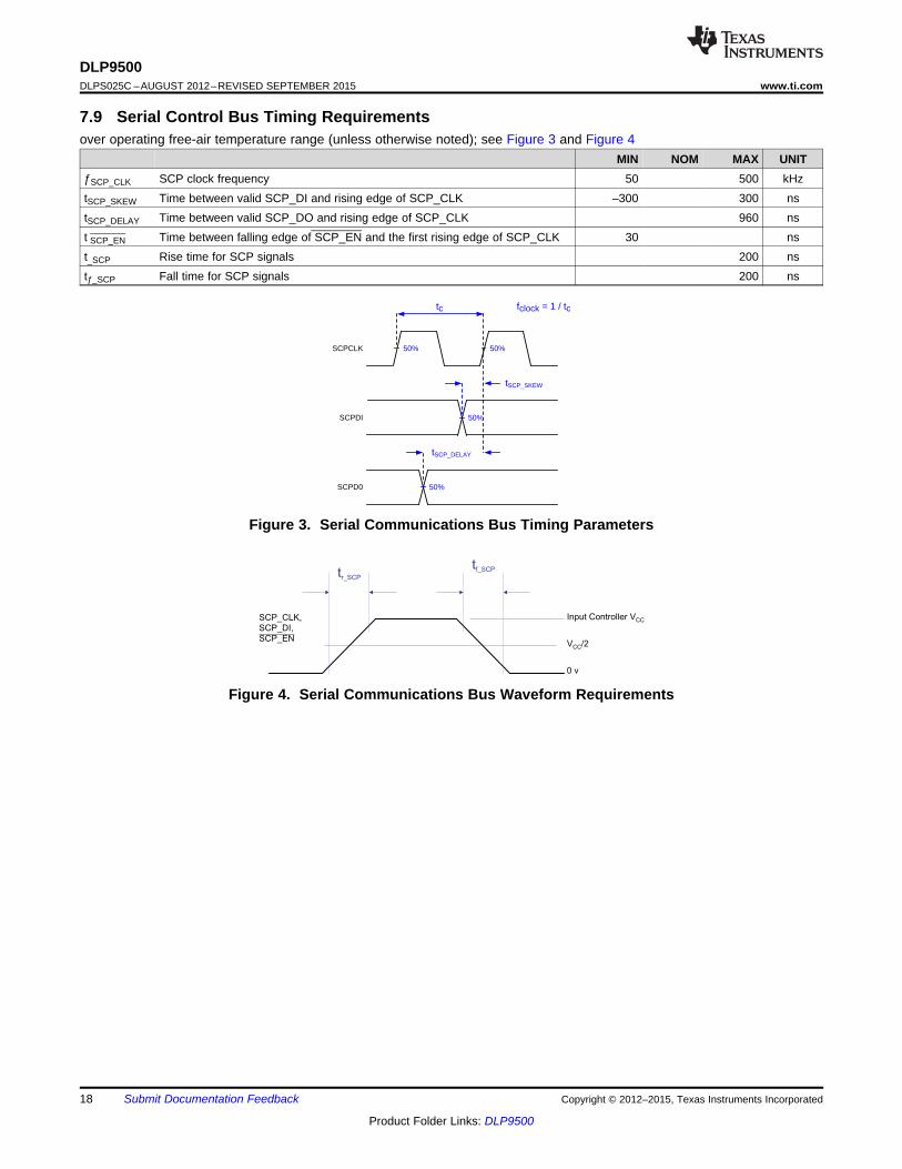
7.9 Serial Control Bus Timing Requirementsover operating free-air temperature range (unless otherwise noted); see Figure 3 and Figure 4
MIN NOM MAX UNITƒSCP_CLK SCP clock frequency 50 500 kHztSCP_SKEW Time between valid SCP_DI and rising edge of SCP_CLK –300 300 nstSCP_DELAY Time between valid SCP_DO and rising edge of SCP_CLK 960 nst SCP_EN Time between falling edge of SCP_EN and the first rising edge of SCP_CLK 30 nst_SCP Rise time for SCP signals 200 nstƒ_SCP Fall time for SCP signals 200 ns
Figure 3. Serial Communications Bus Timing Parameters
Figure 4. Serial Communications Bus Waveform Requirements
18 Submit Documentation Feedback Copyright © 2012–2015, Texas Instruments Incorporated
Product Folder Links: DLP9500
Other Area
Thermal
Interface Area
Electrical
Interface Area
Datum ‘A’ Areas
DLP9500www.ti.com DLPS025C –AUGUST 2012–REVISED SEPTEMBER 2015
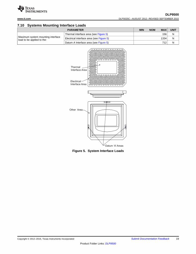
7.10 Systems Mounting Interface LoadsPARAMETER MIN NOM MAX UNIT
Thermal interface area (see Figure 5) 156 NMaximum system mounting interface Electrical interface area (see Figure 5) 1334 Nload to be applied to the:
Datum A Interface area (see Figure 5) 712 N
Figure 5. System Interface Loads
Copyright © 2012–2015, Texas Instruments Incorporated Submit Documentation Feedback 19
Product Folder Links: DLP9500
N ± 1
0 1 2
012
M ±
1
DMD Active Array
3
N ± 4
3 M ±
2
M ±
3
M ±
4
N ± 2N ± 3
M x P
N x PM x N Micromirrors
P P
P
Border micromirrors omitted for clarity.
Not to scale.
P
Details omitted for clarity.
DLP9500DLPS025C –AUGUST 2012–REVISED SEPTEMBER 2015 www.ti.com
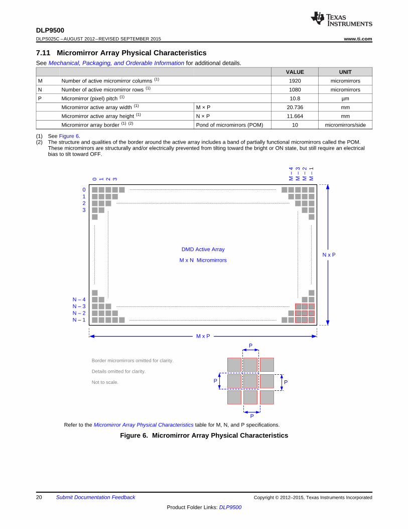
7.11 Micromirror Array Physical CharacteristicsSee Mechanical, Packaging, and Orderable Information for additional details.
VALUE UNITM Number of active micromirror columns (1) 1920 micromirrorsN Number of active micromirror rows (1) 1080 micromirrorsP Micromirror (pixel) pitch (1) 10.8 µm
Micromirror active array width (1) M × P 20.736 mmMicromirror active array height (1) N × P 11.664 mmMicromirror array border (1) (2) Pond of micromirrors (POM) 10 micromirrors/side
(1) See Figure 6.(2) The structure and qualities of the border around the active array includes a band of partially functional micromirrors called the POM.
These micromirrors are structurally and/or electrically prevented from tilting toward the bright or ON state, but still require an electricalbias to tilt toward OFF.
Refer to the Micromirror Array Physical Characteristics table for M, N, and P specifications.
Figure 6. Micromirror Array Physical Characteristics
20 Submit Documentation Feedback Copyright © 2012–2015, Texas Instruments Incorporated
Product Folder Links: DLP9500
DLP9500www.ti.com DLPS025C –AUGUST 2012–REVISED SEPTEMBER 2015
7.12 Micromirror Array Optical CharacteristicsTI assumes no responsibility for end-equipment optical performance. Achieving the desired end-equipment opticalperformance involves making trade-offs between numerous component and system design parameters. See the relatedapplication reports (listed in Related Documentation) for guidelines.
PARAMETER TEST CONDITIONS MIN TYP MAX UNITDMD parked state (1) (2) (3), 0See Figure 12
a Micromirror tilt angle degreesDMD landed state (1) (4) (5) 12See Figure 12
β Micromirror tilt angle variation (1) (4) (6) (7) (8) See Figure 12 –1 1 degreesMicromirror crossover time (9) 16 22 µsMicromirror switching time at 400 MHz with global 56 µsreset (10)
Non-adjacent micromirrors 10Non-operating micromirrors (11) micromirrors
Adjacent micromirrors 0Orientation of the micromirror axis-of-rotation (12) See Figure 12 44 45 46 degrees
400 to 700 nm, with allMicromirror array optical efficiency (13) (14) 68%micromirrors in the ON state
(1) Measured relative to the plane formed by the overall micromirror array(2) Parking the micromirror array returns all of the micromirrors to an essentially flat (0˚) state (as measured relative to the plane formed by
the overall micromirror array).(3) When the micromirror array is parked, the tilt angle of each individual micromirror is uncontrolled.(4) Additional variation exists between the micromirror array and the package datums, as shown in Mechanical, Packaging, and Orderable
Information.(5) When the micromirror array is landed, the tilt angle of each individual micromirror is dictated by the binary contents of the CMOS
memory cell associated with each individual micromirror. A binary value of 1 results in a micromirror landing in an nominal angularposition of +12°. A binary value of 0 results in a micromirror landing in an nominal angular position of –12°.
(6) Represents the landed tilt angle variation relative to the nominal landed tilt angle.(7) Represents the variation that can occur between any two individual micromirrors, located on the same device or located on different
devices.(8) For some applications, it is critical to account for the micromirror tilt angle variation in the overall system optical design. With some
system optical designs, the micromirror tilt angle variation within a device may result in perceivable non-uniformities in the light fieldreflected from the micromirror array. With some system optical designs, the micromirror tilt angle variation between devices may result incolorimetry variations and/or system contrast variation.
(9) Micromirror crossover time is primarily a function of the natural response time of the micromirrors.(10) Micromirror switching is controlled and coordinated by the DLPC410 (DLPS024) and DLPA200 (DLPS015). Nominal switching time
depends on the system implementation and represents the time for the entire micromirror array to be refreshed.(11) Non-operating micromirror is defined as a micromirror that is unable to transition nominally from the –12° position to +12° or vice versa.(12) Measured relative to the package datums 'B' and 'C', shown in the Mechanical, Packaging, and Orderable Information.(13) The minimum or maximum DMD optical efficiency observed in a specific application depends on numerous application-specific design
variables, such as:(a) Illumination wavelength, bandwidth/line-width, degree of coherence(b) Illumination angle, plus angle tolerance(c) Illumination and projection aperture size, and location in the system optical path(d) Illumination overfill of the DMD micromirror array(e) Aberrations present in the illumination source and/or path(f) Aberrations present in the projection path
The specified nominal DMD optical efficiency is based on the following use conditions:(a) Visible illumination (400 to 700 nm )(b) Input illumination optical axis oriented at 24° relative to the window normal(c) Projection optical axis oriented at 0° relative to the window normal(d) ƒ / 3 illumination aperture(e) ƒ / 2.4 projection aperture
Based on these use conditions, the nominal DMD optical efficiency results from the following four components:(a) Micromirror array fill factor: nominally 92%(b) Micromirror array diffraction efficiency: nominally 86%(c) Micromirror surface reflectivity: nominally 88%(d) Window transmission: nominally 97% (single pass, through two surface transitions)
(14) Does not account for the effect of micromirror switching duty cycle, which is application dependent. Micromirror switching duty cyclerepresents the percentage of time that the micromirror is actually reflecting light from the optical illumination path to the optical projectionpath. This duty cycle depends on the illumination aperture size, the projection aperture size, and the micromirror array update rate.
Copyright © 2012–2015, Texas Instruments Incorporated Submit Documentation Feedback 21
Product Folder Links: DLP9500
DLP9500DLPS025C –AUGUST 2012–REVISED SEPTEMBER 2015 www.ti.com
7.13 Window Characteristics
PARAMETER (1) TEST CONDITIONS MIN TYP MAX UNITWindow material designation Corning 7056Window refractive index At wavelength 589 nm 1.487Window flatness (2) Per 25 mm 4 fringesWindow artifact size Within the Window Aperture (3) 400 µmWindow aperture See (4)
Illumination overfill Refer to Illumination OverfillAt wavelength 405 nm. Applies to 0° and 24° AOI only. 95%Minimum within the wavelength range 420 nm to 680 nm.Window transmittance, single–pass 97%Applies to all angles 0° to 30° AOI.through both surfaces and glass (5)
Average over the wavelength range 420 nm to 680 nm. 97%Applies to all angles 30° to 45° AOI.
(1) See Window Characteristics and Optics for more information.(2) At a wavelength of 632.8 nm.(3) See the Mechanical, Packaging, and Orderable Information section at the end of this document for details regarding the size and
location of the window aperture.(4) For details regarding the size and location of the window aperture, see the package mechanical characteristics listed in the Mechanical
ICD in the Mechanical, Packaging, and Orderable Information section.(5) See the TI application report DLPA031, Wavelength Transmittance Considerations for DLP DMD Window.
Figure 7. Max Recommended DMD Temperature – Derating Curve
22 Submit Documentation Feedback Copyright © 2012–2015, Texas Instruments Incorporated
Product Folder Links: DLP9500
DLP9500www.ti.com DLPS025C –AUGUST 2012–REVISED SEPTEMBER 2015
7.14 Chipset Component Usage SpecificationThe DLP9500 is a component of one or more DLP chipsets. Reliable function and operation of the DLP9500requires that it be used in conjunction with the other components of the applicable DLP chipset, including thosecomponents that contain or implement TI DMD control technology. TI DMD control technology is the TItechnology and devices for operating or controlling a DLP DMD.
Copyright © 2012–2015, Texas Instruments Incorporated Submit Documentation Feedback 23
Product Folder Links: DLP9500
DLP9500DLPS025C –AUGUST 2012–REVISED SEPTEMBER 2015 www.ti.com
8 Detailed Description
8.1 OverviewOptically, the DLP9500 consists of 2,073,600 highly reflective, digitally switchable, micrometer-sized mirrors(micromirrors), organized in a two-dimensional array of 1920 micromirror columns by 1080 micromirror rows ().Each aluminum micromirror is approximately 10.8 microns in size (see the Micromirror Pitch in ) and isswitchable between two discrete angular positions: –12° and 12°. The angular positions are measured relative toa 0° flat state, which is parallel to the array plane (see Figure 12). The tilt direction is perpendicular to the hinge-axis, which is positioned diagonally relative to the overall array. The On State landed position is directed towardrow 0, column 0 (upper left) corner of the device package (see the Micromirror Hinge-Axis Orientation in ). In thefield of visual displays, the 1920 × 1080 pixel resolution is referred to as 1080p.
Each individual micromirror is positioned over a corresponding CMOS memory cell. The angular position of aspecific micromirror is determined by the binary state (logic 0 or 1) of the corresponding CMOS memory cellcontents, after the mirror clocking pulse is applied. The angular position (–12° or +12°) of the individualmicromirrors changes synchronously with a micromirror clocking pulse, rather than being synchronous with theCMOS memory cell data update. Therefore, writing a logic 1 into a memory cell followed by a mirror clockingpulse will result in the corresponding micromirror switching to a 12° position. Writing a logic 0 into a memory cellfollowed by a mirror clocking pulse will result in the corresponding micromirror switching to a –12° position.
Updating the angular position of the micromirror array consists of two steps. First, updating the contents of theCMOS memory. Second, application of a micromirror clocking pulse to all or a portion of the micromirror array(depending upon the configuration of the system). Micromirror clocking pulses are generated externally by twoDLPA200s, with application of the pulses being coordinated by the DLPC410 controller.
Around the perimeter of the 1920 by 1080 array of micromirrors is a uniform band of border micromirrors. Theborder micromirrors are not user-addressable. The border micromirrors land in the –12° position once power hasbeen applied to the device. There are 10 border micromirrors on each side of the 1920 by 1080 active array.
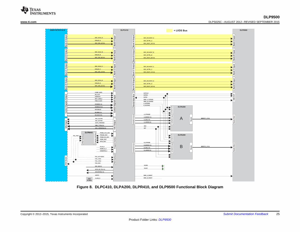
Figure 8 shows a DLPC410 and DLP9500 chipset block diagram. The DLPC410 and DLPA200s control andcoordinate the data loading and micromirror switching for reliable DLP9500 operation. The DLPR410 is theprogrammed PROM required to properly configure the DLPC410 controller. For more information on the chipsetcomponents, see Application and Implementation. For a typical system application using the DLP Discovery 4100chipset including a DLP9500, see Figure 18.
8.2 Functional Block DiagramFigure 8 shows a simplified system block diagram with the use of the DLPC410 with the following chipsetcomponents:
DLPC410 Xilinx [XC5VLX30] FPGA configured to provide high-speed DMD data and control, and DLPA200timing and control
DLPR410 [XCF16PFSG48C] serial flash PROM contains startup configuration information (EEPROM)
DLPA200 Two DMD micromirror drivers for the DLP9500 DMD
DLP9500 Spatial light modulator (DMD)
24 Submit Documentation Feedback Copyright © 2012–2015, Texas Instruments Incorporated
Product Folder Links: DLP9500
PROM_CCK_DDC
PROM_DO_DDC
PROGB_DDC
DONE_DDC
INTB_DDC
DLPC410
Ban
kA
Inp
ut
DDC_DCLK_A
DVALID_A
DDC_DIN_A(15:0)
Ban
k B
In
pu
t
DDC_DCLK_B
DVALID_B
DDC_DIN_B(15:0)
Ban
k C
In
pu
t
DDC_DCLK_C
DVALID_C
DDC_DIN_C(15:0)
Ban
k D
In
pu
t
DDC_DCLK_D
DVALID_D
DDC_DIN_D(15:0)
DDC_DCLKOUT_D
DDC_SCTRL_D
DDC_DOUT_D(15:0)
DDC_DCLKOUT_A
DDC_SCTRL_A
DDC_DOUT_A(15:0)
Ban
kA
Ou
tpu
t
DDC_DCLKOUT_B
DDC_SCTRL_B
DDC_DOUT_B(15:0)
Ban
k B
Ou
tpu
t
DDC_DCLKOUT_C
DDC_SCTRL_C
DDC_DOUT_C(15:0)
Ban
k C
Ou
tpu
tB
an
k B
Ou
tpu
t
DLP9500
Ban
kA
Inp
ut
Ban
k B
In
pu
tB
an
k C
In
pu
tB
an
k B
In
pu
t
Seri
al D
ata
Bu
s
CLKIN_R
RST_ACTIVE
ARSTZ
Info
Ou
tpu
t
DMD_TYPE(3:0)
INIT_ACTIVE
DDC_VERSION(2:0)
ECP2_FINISHED
DLPA200
OSC50 Mhz
DLPR410
MBRST1_(15:0)A_MODE(1:0)
A_STROBE
A_ADDR(3:0)
A_SEL(1:0) A
INIT
OEZ
DMD_A_SCPENZ
DMD_B_SCPENZ
DMD_A_RESET
DMD_B_RESET
A_SCPENZ
SCPDO
SCPCLK
B_SCPENZ
DLPA200
MBRST2_(15:0)B_MODE(1:0)
B_STROBE
B_ADDR(3:0)
B_SEL(1:0) B
DL
PA
200
AIn
pu
tD
LP
A200 B
In
pu
t
DL
PA
20
0A
Ou
tpu
tD
LP
A2
00
B O
utp
ut
DL
PA
20
0A
SC
PD
LP
A20
0 B
SC
P
DM
D S
CP
Resets
Sid
e 1
Resets
Sid
e 2
ECP2_M_TP(31:0)
DDCSPARE(1:0)
VLED0
VLED1
DDC_M(2:0)
Pro
gra
m I
nte
rfa
ce
JTA
G I
nte
rfa
ce
TDO_XCF16DDC
TCK_JTAG
TDO_DDC
USER INTERFACE
JTA
G I
nte
rfa
ce
Pro
gra
m I
nte
rfa
ce
TDI_JTAG
JTA
G H
ea
de
r
CS_B_0
RDWR_B_0
HSWAPEN_0
TCK_JTAG
Info
In
pu
tB
an
k D
Ou
tpu
tB
an
k C
Ou
tpu
tB
an
k B
Ou
tpu
tB
an
kA
Ou
tpu
t
= LVDS Bus
SCPDI
Resets
Resets
Co
ntr
ol S
ign
als
In
pu
t
ROWMD(1:0)
ROWAD(10:0)
BLKMD(1:0)
BLKAD(10:0)
COMP_DATA
NS_FLIP
STEPVCC
WDT_ENBLZ
PWR_FLOAT
Co
ntr
ol S
ign
als
Ou
tpu
t
RST2BLKZ
DLP9500www.ti.com DLPS025C –AUGUST 2012–REVISED SEPTEMBER 2015
Figure 8. DLPC410, DLPA200, DLPR410, and DLP9500 Functional Block Diagram
Copyright © 2012–2015, Texas Instruments Incorporated Submit Documentation Feedback 25
Product Folder Links: DLP9500
DLP9500DLPS025C –AUGUST 2012–REVISED SEPTEMBER 2015 www.ti.com
8.3 Feature Description
Table 1. DMD OverviewSINGLE BLOCK GLOBAL RESET DATA RATEDMD ARRAY MODE MODE MIRROR PITCH(GIGA PIXELS/s)(PATTERNS/s) (PATTERNS/s)
DLP9500 - 0.95" 1080p 1920 × 1080 23148 17857 48 10.8 μm
8.3.1 DLPC410 ControllerThe DLPC410 chipset includes the DLPC410 controller which provides a high-speed LVDS data and controlinterface for DMD control. This interface is also connected to a second FPGA used to drive applications (notincluded in the chipset). The DLPC410 generates DMD and DLPA200 initialization and control signals inresponse to the inputs on the control interface.
For more information, see the DLPC410 data sheet (DLPS024).
8.3.2 DLPA200 DMD Micromirror DriversDLPA200 micromirror drivers provide the micromirror clocking pulse driver functions for the DMD. Two driversare required for DLP9500.
The DLPA200 is designed to work with multiple DLP chipsets. Although the DLPA200 contains 16 MBSRT outputpins, only 15 lines are used with the DLP9500 chipset. For more information see and the DLPA200 data sheet(DLPS015).
8.3.3 Flash Configuration PROMThe DLPC410 is configured at startup from the serial flash PROM. The contents of this PROM can not bealtered. For more information, see the DLPC410 data sheet (DLPS024) and DLPR410 data sheet (DLPS027).
8.3.4 DMD
8.3.4.1 DLP9500 1080p Chipset InterfacesThis section will describe the interface between the different components included in the chipset. For moreinformation on component interfacing, see Application and Implementation.
8.3.4.1.1 DLPC410 Interface Description
8.3.4.1.1.1 DLPC410 IO
Table 2 describes the inputs and outputs of the DLPC410 to the user. For more details on these signals, see theDLPC410 data sheet (DLPS024).
26 Submit Documentation Feedback Copyright © 2012–2015, Texas Instruments Incorporated
Product Folder Links: DLP9500
DLP9500www.ti.com DLPS025C –AUGUST 2012–REVISED SEPTEMBER 2015
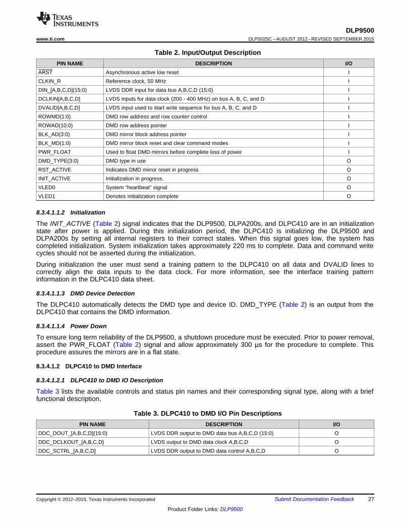
Table 2. Input/Output DescriptionPIN NAME DESCRIPTION I/O
ARST Asynchronous active low reset ICLKIN_R Reference clock, 50 MHz IDIN_[A,B,C,D](15:0) LVDS DDR input for data bus A,B,C,D (15:0) IDCLKIN[A,B,C,D] LVDS inputs for data clock (200 - 400 MHz) on bus A, B, C, and D IDVALID[A,B,C,D] LVDS input used to start write sequence for bus A, B, C, and D IROWMD(1:0) DMD row address and row counter control IROWAD(10:0) DMD row address pointer IBLK_AD(3:0) DMD mirror block address pointer IBLK_MD(1:0) DMD mirror block reset and clear command modes IPWR_FLOAT Used to float DMD mirrors before complete loss of power IDMD_TYPE(3:0) DMD type in use ORST_ACTIVE Indicates DMD mirror reset in progress OINIT_ACTIVE Initialization in progress. OVLED0 System “heartbeat” signal OVLED1 Denotes initialization complete O
8.3.4.1.1.2 Initialization
The INIT_ACTIVE (Table 2) signal indicates that the DLP9500, DLPA200s, and DLPC410 are in an initializationstate after power is applied. During this initialization period, the DLPC410 is initializing the DLP9500 andDLPA200s by setting all internal registers to their correct states. When this signal goes low, the system hascompleted initialization. System initialization takes approximately 220 ms to complete. Data and command writecycles should not be asserted during the initialization.
During initialization the user must send a training pattern to the DLPC410 on all data and DVALID lines tocorrectly align the data inputs to the data clock. For more information, see the interface training patterninformation in the DLPC410 data sheet.
8.3.4.1.1.3 DMD Device Detection
The DLPC410 automatically detects the DMD type and device ID. DMD_TYPE (Table 2) is an output from theDLPC410 that contains the DMD information.
8.3.4.1.1.4 Power Down
To ensure long term reliability of the DLP9500, a shutdown procedure must be executed. Prior to power removal,assert the PWR_FLOAT (Table 2) signal and allow approximately 300 µs for the procedure to complete. Thisprocedure assures the mirrors are in a flat state.
8.3.4.1.2 DLPC410 to DMD Interface
8.3.4.1.2.1 DLPC410 to DMD IO Description
Table 3 lists the available controls and status pin names and their corresponding signal type, along with a brieffunctional description.
Table 3. DLPC410 to DMD I/O Pin DescriptionsPIN NAME DESCRIPTION I/O
DDC_DOUT_[A,B,C,D](15:0) LVDS DDR output to DMD data bus A,B,C,D (15:0) ODDC_DCLKOUT_[A,B,C,D] LVDS output to DMD data clock A,B,C,D ODDC_SCTRL_[A,B,C,D] LVDS DDR output to DMD data control A,B,C,D O
Copyright © 2012–2015, Texas Instruments Incorporated Submit Documentation Feedback 27
Product Folder Links: DLP9500
DLPC410
LVDS BUS D
s
s
s
DIN_D(15:0)DCLK_DDVALID_D
LV
DS
BU
S B
sss DIN
_B
(15
:0)
DC
LK
_B
DV
AL
ID_
B
LVDS BUS C
s
s
s
DIN_C(15:0)DCLK_CDVALID_C
LV
DS
BU
SA
sss DIN
_A
(15
:0)
DC
LK
_A
DV
AL
ID_
A
LV
DS
BU
S B
ss DIN
_B
(15
:0)
DC
LK
_B
sDV
AL
ID_
B
LV
DS
BU
S C
ss DO
UT
_C
(15
:0)
DC
LK
OU
T_
CsS
CT
RL
_C
LVDS BUS D
s
s
DOUT_D(15:0)DCLKOUT_DsSCTRL_D
LVDS BUS A
s
s
DOUT_A(15:0)DCLKOUT_AsSCTRL_A
DLP9500DLPS025C –AUGUST 2012–REVISED SEPTEMBER 2015 www.ti.com
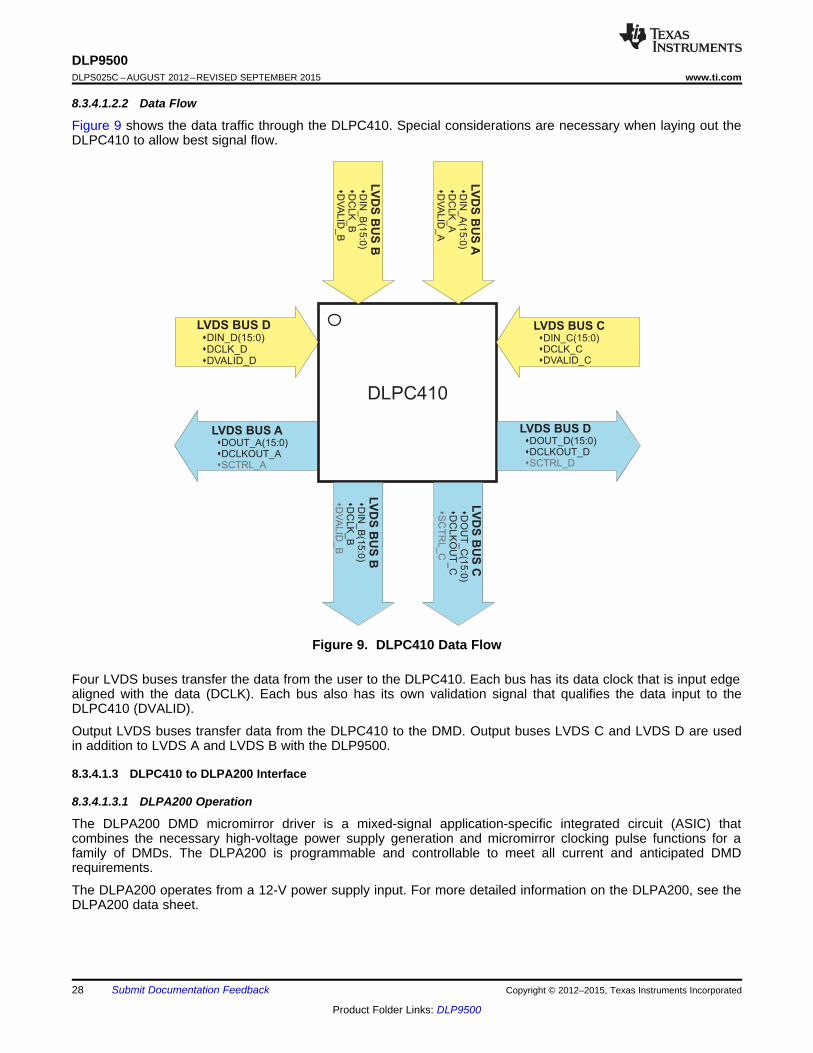
8.3.4.1.2.2 Data Flow
Figure 9 shows the data traffic through the DLPC410. Special considerations are necessary when laying out theDLPC410 to allow best signal flow.
Figure 9. DLPC410 Data Flow
Four LVDS buses transfer the data from the user to the DLPC410. Each bus has its data clock that is input edgealigned with the data (DCLK). Each bus also has its own validation signal that qualifies the data input to theDLPC410 (DVALID).
Output LVDS buses transfer data from the DLPC410 to the DMD. Output buses LVDS C and LVDS D are usedin addition to LVDS A and LVDS B with the DLP9500.
8.3.4.1.3 DLPC410 to DLPA200 Interface
8.3.4.1.3.1 DLPA200 Operation
The DLPA200 DMD micromirror driver is a mixed-signal application-specific integrated circuit (ASIC) thatcombines the necessary high-voltage power supply generation and micromirror clocking pulse functions for afamily of DMDs. The DLPA200 is programmable and controllable to meet all current and anticipated DMDrequirements.
The DLPA200 operates from a 12-V power supply input. For more detailed information on the DLPA200, see theDLPA200 data sheet.
28 Submit Documentation Feedback Copyright © 2012–2015, Texas Instruments Incorporated
Product Folder Links: DLP9500
DLPC410
SCP bus
SCP bus
DLPA200
DLPA200
DLP9500www.ti.com DLPS025C –AUGUST 2012–REVISED SEPTEMBER 2015
8.3.4.1.3.2 DLPC410 to DLPA200 IO Description
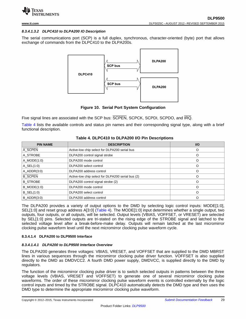
The serial communications port (SCP) is a full duplex, synchronous, character-oriented (byte) port that allowsexchange of commands from the DLPC410 to the DLPA200s.
Figure 10. Serial Port System Configuration
Five signal lines are associated with the SCP bus: SCPEN, SCPCK, SCPDI, SCPDO, and IRQ.
Table 4 lists the available controls and status pin names and their corresponding signal type, along with a brieffunctional description.
Table 4. DLPC410 to DLPA200 I/O Pin DescriptionsPIN NAME DESCRIPTION I/O
A_SCPEN Active-low chip select for DLPA200 serial bus OA_STROBE DLPA200 control signal strobe OA_MODE(1:0) DLPA200 mode control OA_SEL(1:0) DLPA200 select control OA_ADDR(3:0) DLPA200 address control OB_SCPEN Active-low chip select for DLPA200 serial bus (2) OB_STROBE DLPA200 control signal strobe (2) OB_MODE(1:0) DLPA200 mode control OB_SEL(1:0) DLPA200 select control OB_ADDR(3:0) DLPA200 address control O
The DLPA200 provides a variety of output options to the DMD by selecting logic control inputs: MODE[1:0],SEL[1:0] and reset group address A[3:0] (Table 4). The MODE[1:0] input determines whether a single output, twooutputs, four outputs, or all outputs, will be selected. Output levels (VBIAS, VOFFSET, or VRESET) are selectedby SEL[1:0] pins. Selected outputs are tri-stated on the rising edge of the STROBE signal and latched to theselected voltage level after a break-before-make delay. Outputs will remain latched at the last micromirrorclocking pulse waveform level until the next micromirror clocking pulse waveform cycle.
8.3.4.1.4 DLPA200 to DLP9500 Interface
8.3.4.1.4.1 DLPA200 to DLP9500 Interface Overview
The DLPA200 generates three voltages: VBIAS, VRESET, and VOFFSET that are supplied to the DMD MBRSTlines in various sequences through the micromirror clocking pulse driver function. VOFFSET is also supplieddirectly to the DMD as DMDVCC2. A fourth DMD power supply, DMDVCC, is supplied directly to the DMD byregulators.
The function of the micromirror clocking pulse driver is to switch selected outputs in patterns between the threevoltage levels (VBIAS, VRESET and VOFFSET) to generate one of several micromirror clocking pulsewaveforms. The order of these micromirror clocking pulse waveform events is controlled externally by the logiccontrol inputs and timed by the STROBE signal. DLPC410 automatically detects the DMD type and then uses theDMD type to determine the appropriate micromirror clocking pulse waveform.
Copyright © 2012–2015, Texas Instruments Incorporated Submit Documentation Feedback 29
Product Folder Links: DLP9500
From OutputUnder Test
TesterChannel
LOAD CIRCUIT
C = 50 pF
C = 5 pF for Disable TimeL
L
RL
DLP9500DLPS025C –AUGUST 2012–REVISED SEPTEMBER 2015 www.ti.com
A direct micromirror clocking pulse operation causes a mirror to transition directly from one latched state to thenext. The address must already be set up on the mirror electrodes when the micromirror clocking pulse isinitiated. Where the desired mirror display period does not allow for time to set up the address, a micromirrorclocking pulse with release can be performed. This operation allows the mirror to go to a relaxed state regardlessof the address while a new address is set up, after which the mirror can be driven to a new latched state.
A mirror in the relaxed state typically reflects light into a system collection aperture and can be thought of as offalthough the light is likely to be more than a mirror latched in the off state. System designers should carefullyevaluate the impact of relaxed mirror conditions on optical performance.
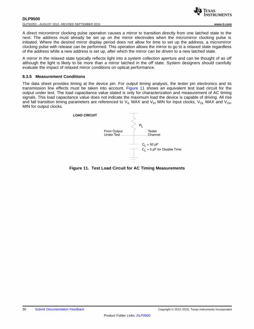
8.3.5 Measurement ConditionsThe data sheet provides timing at the device pin. For output timing analysis, the tester pin electronics and itstransmission line effects must be taken into account. Figure 11 shows an equivalent test load circuit for theoutput under test. The load capacitance value stated is only for characterization and measurement of AC timingsignals. This load capacitance value does not indicate the maximum load the device is capable of driving. All riseand fall transition timing parameters are referenced to VIL MAX and VIH MIN for input clocks, VOL MAX and VOHMIN for output clocks.
Figure 11. Test Load Circuit for AC Timing Measurements
30 Submit Documentation Feedback Copyright © 2012–2015, Texas Instruments Incorporated
Product Folder Links: DLP9500
DLP9500
Package PinA1 Corner
Inci
dent
Illum
inat
ion
Inci
dent
Illum
inat
ion
For Reference
Flat-State( “parked” )
Micromirror Position
“Off-State”Micromirror
“On-State”Micromirror
Silicon SubstrateSilicon Substrate
a ± b -a ± b
Two“On-State”
Micromirrors
Two“Off-State”
Micromirrors
Incid
en
t
Illum
inatio
n-L
igh
tP
ath
Incid
en
t
Illum
inatio
n-L
igh
tP
athP
roje
cte
d-L
igh
tP
ath
Off-
State
-Lig
ht
Path
DLP9500www.ti.com DLPS025C –AUGUST 2012–REVISED SEPTEMBER 2015
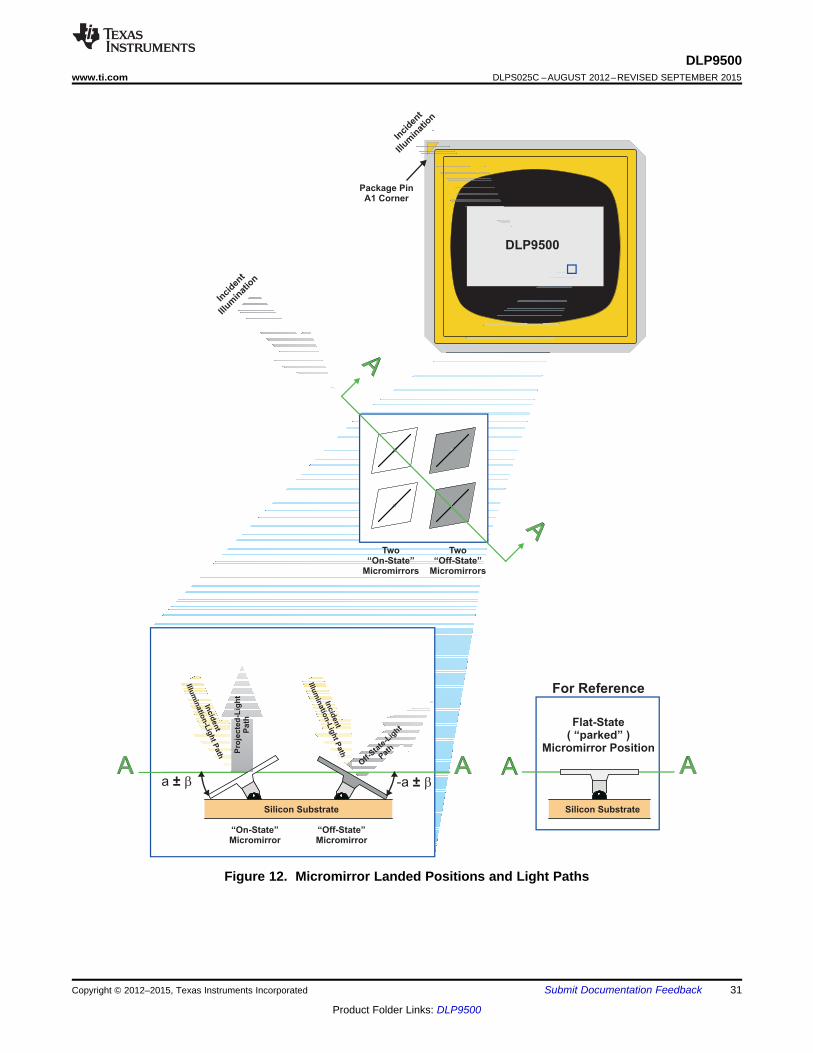
Figure 12. Micromirror Landed Positions and Light Paths
Copyright © 2012–2015, Texas Instruments Incorporated Submit Documentation Feedback 31
Product Folder Links: DLP9500
DLP9500DLPS025C –AUGUST 2012–REVISED SEPTEMBER 2015 www.ti.com
8.4 Device Functional ModesThe DLP9500 has only one functional mode; it is set to be highly optimized for low latency and high speed ingenerating mirror clocking pulses and timings.
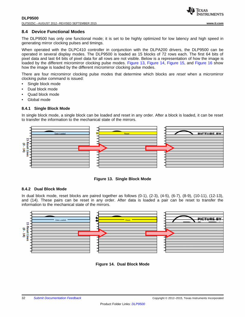
When operated with the DLPC410 controller in conjunction with the DLPA200 drivers, the DLP9500 can beoperated in several display modes. The DLP9500 is loaded as 15 blocks of 72 rows each. The first 64 bits ofpixel data and last 64 bits of pixel data for all rows are not visible. Below is a representation of how the image isloaded by the different micromirror clocking pulse modes. Figure 13, Figure 14, Figure 15, and Figure 16 showhow the image is loaded by the different micromirror clocking pulse modes.
There are four micromirror clocking pulse modes that determine which blocks are reset when a micromirrorclocking pulse command is issued:• Single block mode• Dual block mode• Quad block mode• Global mode
8.4.1 Single Block ModeIn single block mode, a single block can be loaded and reset in any order. After a block is loaded, it can be resetto transfer the information to the mechanical state of the mirrors.
Figure 13. Single Block Mode
8.4.2 Dual Block ModeIn dual block mode, reset blocks are paired together as follows (0-1), (2-3), (4-5), (6-7), (8-9), (10-11), (12-13),and (14). These pairs can be reset in any order. After data is loaded a pair can be reset to transfer theinformation to the mechanical state of the mirrors.
Figure 14. Dual Block Mode
32 Submit Documentation Feedback Copyright © 2012–2015, Texas Instruments Incorporated
Product Folder Links: DLP9500
DLP9500www.ti.com DLPS025C –AUGUST 2012–REVISED SEPTEMBER 2015
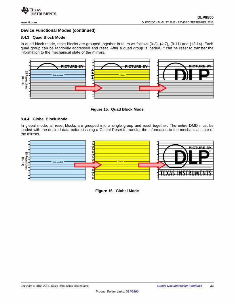
Device Functional Modes (continued)8.4.3 Quad Block ModeIn quad block mode, reset blocks are grouped together in fours as follows (0-3), (4-7), (8-11) and (12-14). Eachquad group can be randomly addressed and reset. After a quad group is loaded, it can be reset to transfer theinformation to the mechanical state of the mirrors.
Figure 15. Quad Block Mode
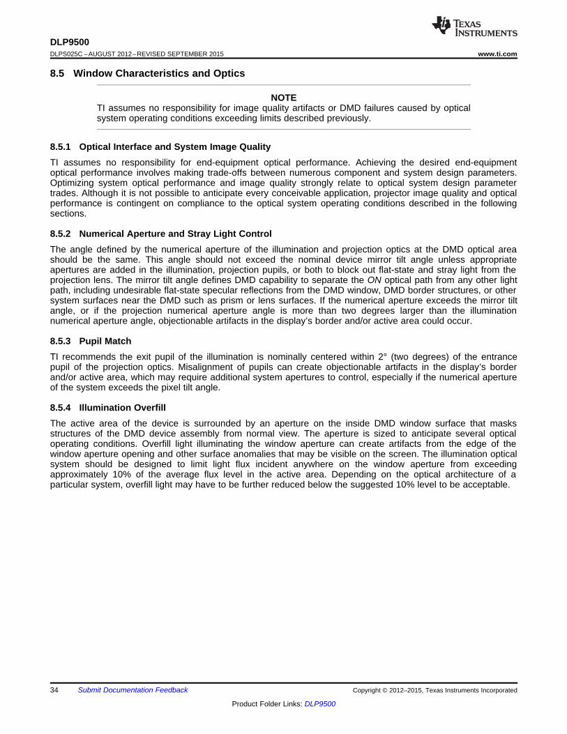
8.4.4 Global Block ModeIn global mode, all reset blocks are grouped into a single group and reset together. The entire DMD must beloaded with the desired data before issuing a Global Reset to transfer the information to the mechanical state ofthe mirrors.
Figure 16. Global Mode
Copyright © 2012–2015, Texas Instruments Incorporated Submit Documentation Feedback 33
Product Folder Links: DLP9500
DLP9500DLPS025C –AUGUST 2012–REVISED SEPTEMBER 2015 www.ti.com
8.5 Window Characteristics and Optics
NOTETI assumes no responsibility for image quality artifacts or DMD failures caused by opticalsystem operating conditions exceeding limits described previously.
8.5.1 Optical Interface and System Image QualityTI assumes no responsibility for end-equipment optical performance. Achieving the desired end-equipmentoptical performance involves making trade-offs between numerous component and system design parameters.Optimizing system optical performance and image quality strongly relate to optical system design parametertrades. Although it is not possible to anticipate every conceivable application, projector image quality and opticalperformance is contingent on compliance to the optical system operating conditions described in the followingsections.
8.5.2 Numerical Aperture and Stray Light ControlThe angle defined by the numerical aperture of the illumination and projection optics at the DMD optical areashould be the same. This angle should not exceed the nominal device mirror tilt angle unless appropriateapertures are added in the illumination, projection pupils, or both to block out flat-state and stray light from theprojection lens. The mirror tilt angle defines DMD capability to separate the ON optical path from any other lightpath, including undesirable flat-state specular reflections from the DMD window, DMD border structures, or othersystem surfaces near the DMD such as prism or lens surfaces. If the numerical aperture exceeds the mirror tiltangle, or if the projection numerical aperture angle is more than two degrees larger than the illuminationnumerical aperture angle, objectionable artifacts in the display’s border and/or active area could occur.
8.5.3 Pupil MatchTI recommends the exit pupil of the illumination is nominally centered within 2° (two degrees) of the entrancepupil of the projection optics. Misalignment of pupils can create objectionable artifacts in the display’s borderand/or active area, which may require additional system apertures to control, especially if the numerical apertureof the system exceeds the pixel tilt angle.
8.5.4 Illumination OverfillThe active area of the device is surrounded by an aperture on the inside DMD window surface that masksstructures of the DMD device assembly from normal view. The aperture is sized to anticipate several opticaloperating conditions. Overfill light illuminating the window aperture can create artifacts from the edge of thewindow aperture opening and other surface anomalies that may be visible on the screen. The illumination opticalsystem should be designed to limit light flux incident anywhere on the window aperture from exceedingapproximately 10% of the average flux level in the active area. Depending on the optical architecture of aparticular system, overfill light may have to be further reduced below the suggested 10% level to be acceptable.
34 Submit Documentation Feedback Copyright © 2012–2015, Texas Instruments Incorporated
Product Folder Links: DLP9500
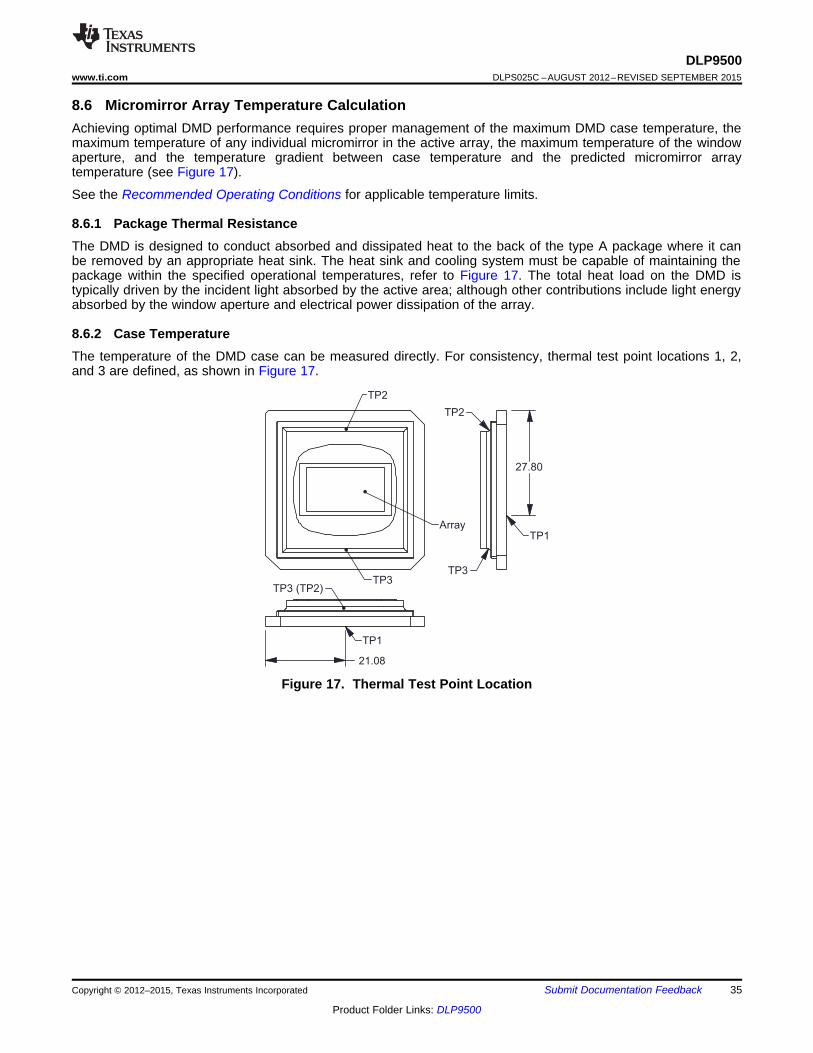
21.08
DLP9500www.ti.com DLPS025C –AUGUST 2012–REVISED SEPTEMBER 2015
8.6 Micromirror Array Temperature CalculationAchieving optimal DMD performance requires proper management of the maximum DMD case temperature, themaximum temperature of any individual micromirror in the active array, the maximum temperature of the windowaperture, and the temperature gradient between case temperature and the predicted micromirror arraytemperature (see Figure 17).
See the Recommended Operating Conditions for applicable temperature limits.
8.6.1 Package Thermal ResistanceThe DMD is designed to conduct absorbed and dissipated heat to the back of the type A package where it canbe removed by an appropriate heat sink. The heat sink and cooling system must be capable of maintaining thepackage within the specified operational temperatures, refer to Figure 17. The total heat load on the DMD istypically driven by the incident light absorbed by the active area; although other contributions include light energyabsorbed by the window aperture and electrical power dissipation of the array.
8.6.2 Case TemperatureThe temperature of the DMD case can be measured directly. For consistency, thermal test point locations 1, 2,and 3 are defined, as shown in Figure 17.
Figure 17. Thermal Test Point Location
Copyright © 2012–2015, Texas Instruments Incorporated Submit Documentation Feedback 35
Product Folder Links: DLP9500
DLP9500DLPS025C –AUGUST 2012–REVISED SEPTEMBER 2015 www.ti.com
Micromirror Array Temperature Calculation (continued)8.6.3 Micromirror Array Temperature CalculationMicromirror array temperature cannot be measured directly; therefore, it must be computed analytically frommeasurement points (Figure 17), the package thermal resistance, the electrical power, and the illumination heatload. The relationship between micromirror array temperature and the case temperature are provided byEquation 1 and Equation 2:
TArray = T Ceramic + (QArray × RArray-To-Ceramic) (1)
QArray = QELE + QILL
where• TArray = Computed micromirror array temperature (°C)• TCeramic = Ceramic temperature (°C) (TP1 location Figure 17)• QArray = Total DMD array power (electrical + absorbed) (measured in Watts)• RArray-To-Ceramic = Thermal resistance of DMD package from array to TP1 (°C/W) (see Package Thermal
Resistance)• QELE = Nominal electrical power (W)• QILL = Absorbed illumination energy (W) (2)
An example calculation is provided based on a traditional DLP video projection system. The electrical powerdissipation of the DMD is variable and depends on the voltages, data rates, and operating frequencies. Thenominal electrical power dissipation used in the calculation is 4.4 W. Thus, QELE = 4.4 W. The absorbed powerfrom the illumination source is variable and depends on the operating state of the mirrors and the intensity of thelight source. Based on modeling and measured data from DLP projection system:
QILL = CL2W × SL
where• CL2W is a lumens to watts constant and can be estimated at 0.00274 W/lm• SL = Screen lumens nominally measured to be 2000 lm• QArray = 4.4 + (0.00274 × 2000) = 9.88 W, estimated total power on micromirror array• TCeramic = 55°C, assumed system measurement (3)
Finally, TArray (micromirror active array temperature) is:TArray= 55°C + (9.88 W × 0.5°C/W) = 59.9°C (4)
36 Submit Documentation Feedback Copyright © 2012–2015, Texas Instruments Incorporated
Product Folder Links: DLP9500
DLP9500www.ti.com DLPS025C –AUGUST 2012–REVISED SEPTEMBER 2015
8.7 Micromirror Landed-On and Landed-Off Duty Cycle
8.7.1 Definition of Micromirror Landed-On/Landed-Off Duty CycleThe micromirror landed-on/landed-off duty cycle (landed duty cycle) denotes the amount of time (as apercentage) that an individual micromirror is landed in the On–state versus the amount of time the samemicromirror is landed in the Off–state.
As an example, a landed duty cycle of 100/0 indicates that the referenced pixel is in the On-state 100% of thetime (and in the Off-state 0% of the time); whereas 0/100 would indicate that the pixel is in the Off-state 100% ofthe time. Likewise, 50/50 indicates that the pixel is On 50% of the time and Off 50% of the time.
Note that when assessing landed duty cycle, the time spent switching from one state (ON or OFF) to the otherstate (OFF or ON) is considered negligible and is thus ignored.
Because a micromirror can only be landed in one state or the other (on or off), the two numbers (percentages)always add to 100.
8.7.2 Landed Duty Cycle and Useful Life of the DMDKnowing the long-term average landed duty cycle (of the end product or application) is important becausesubjecting all (or a portion) of the DMD’s micromirror array (also called the active array) to an asymmetric landedduty cycle for a prolonged period of time can reduce the usable life of the DMD.
Note that it is the symmetry/asymmetry of the landed duty cycle that is of relevance. The symmetry of the landedduty cycle is determined by how close the two numbers (percentages) are to being equal. For example, a landedduty cycle of 50/50 is perfectly symmetrical whereas a landed duty cycle of 100/0 or 0/100 is perfectlyasymmetrical.
8.7.3 Landed Duty Cycle and Operational DMD TemperatureOperational DMD temperature and landed duty cycle interact to affect the usable life of the DMD, and thisinteraction can be exploited to reduce the impact that an asymmetrical landed duty cycle has on the DMD’susable life. This is quantified in the derating curve shown in Figure 7. The importance of this curve is that:• All points along this curve represent the same usable life.• All points above this curve represent lower usable life (and the further away from the curve, the lower the
usable life).• All points below this curve represent higher usable life (and the further away from the curve, the higher the
usable life).
In practice, this curve specifies the maximum operating DMD temperature that the DMD should be operated atfor a give long-term average landed duty.
8.7.4 Estimating the Long-Term Average Landed Duty Cycle of a Product or ApplicationDuring a given period of time, the landed duty cycle of a given pixel follows from the image content beingdisplayed by that pixel.
For example, in the simplest case, when displaying pure-white on a given pixel for a given time period, that pixelwill experience a 100/0 landed duty cycle during that time period. Likewise, when displaying pure-black, the pixelwill experience a 0/100 landed duty cycle.
Between the two extremes (ignoring for the moment color and any image processing that may be applied to anincoming image), the landed duty cycle tracks one-to-one with the gray scale value, as shown in Table 5.
Copyright © 2012–2015, Texas Instruments Incorporated Submit Documentation Feedback 37
Product Folder Links: DLP9500
DLP9500DLPS025C –AUGUST 2012–REVISED SEPTEMBER 2015 www.ti.com
Table 5. Grayscale Value and Landed Duty CycleGRAYSCALE VALUE LANDED DUTY CYCLE
0% 0/10010% 10/9020% 20/8030% 30/7040% 40/6050% 50/5060% 60/4070% 70/3080% 80/2090% 90/10100% 100/0
Accounting for color rendition (but still ignoring image processing) requires knowing both the color intensity (from0% to 100%) for each constituent primary color (red, green, and/or blue) for the given pixel as well as the colorcycle time for each primary color, where “color cycle time” is the total percentage of the frame time that a givenprimary must be displayed to achieve the desired white point.
During a given period of time, the landed duty cycle of a given pixel can be calculated as follows:
Landed Duty Cycle = (Red_Cycle_% × Red_Scale_Value) + (Green_Cycle_% × Green_Scale_Value) +(Blue_Cycle_% × Blue_Scale_Value)
where:Red_Cycle_%, Green_Cycle_%, and Blue_Cycle_%, represent the percentage of the frame time that Red,Green, and Blue are displayed (respectively) to achieve the desired white point.
For example, assume that the red, green and blue color cycle times are 50%, 20%, and 30% respectively (toachieve the desired white point), then the landed duty for various combinations of red, green, blue colorintensities would be as shown in Table 6.
Table 6. Example Landed Duty Cycle for Full-ColorRED CYCLE PERCENTAGE GREEN CYCLE PERCENTAGE BLUE CYCLE PERCENTAGE
50% 20% 30% LANDED DUTY CYCLERED SCALE VALUE GREEN SCALE VALUE BLUE SCALE VALUE
0% 0% 0% 0/100100% 0% 0% 50/50
0% 100% 0% 20/800% 0% 100% 30/70
12% 0% 0% 6/940% 35% 0% 7/930% 0% 60% 18/82
100% 100% 0% 70/300% 100% 100% 50/50
100% 0% 100% 80/2012% 35% 0% 13/870% 35% 60% 25/75
12% 0% 60% 24/76100% 100% 100% 100/0
38 Submit Documentation Feedback Copyright © 2012–2015, Texas Instruments Incorporated
Product Folder Links: DLP9500
DLP9500www.ti.com DLPS025C –AUGUST 2012–REVISED SEPTEMBER 2015
9 Application and Implementation
NOTEInformation in the following applications sections is not part of the TI componentspecification, and TI does not warrant its accuracy or completeness. TI’s customers areresponsible for determining suitability of components for their purposes. Customers shouldvalidate and test their design implementation to confirm system functionality.
9.1 Application InformationThe DLP9500 devices must be coupled with the DLPC410 controller to provide a reliable solution for manydifferent applications. The DMDs are spatial light modulators which reflect incoming light from an illuminationsource to one of two directions, with the primary direction being into a projection collection optic. Each applicationis derived primarily from the optical architecture of the system and the format of the data coming into theDLPC410. Applications of interest include 3D printing, lithography, medical systems, and compressive sensing.
Copyright © 2012–2015, Texas Instruments Incorporated Submit Documentation Feedback 39
Product Folder Links: DLP9500
DLPC410
LVDS BUS (A,B,[C,D])DDC_DCLK, DVALID, DDC_DIN(15:0)
LVDS BUS (A,B,[C,D])DDC_DCLKOUT, DDCSCTRL, DDC_DOUT(15:0)
CLKIN_R
CONTROL SIGNALSCOMP_DATA, NS_FLIP, WDT_ENBLZ, PWR_FLOAT
ARSTZ
DLPC410 INFO SIGNALSRST_ACTIVE, INIT_ACTIVE, ECP2_FINISHED,
DMD_TYPE(3:0), DDC_VERSION(2:0)
DLPA200
OSC50 Mhz
DLPR410
DLPA200 CONTROLA_MODE(1:0), A_SEL(1:0),
A_ADDR(3:0), OEZ, INIT
A
VLED0
VLED1
USER - MAINPROCESSOR / FPGA
ROW and BLOCK SIGNALSROWMD(1:0), ROWAD(10:0), BLKMD(1:0), BLKAD(3:0), RST2BLKZ
SCP BUSSCPCLK, SCPDO, SCPDI, DMD_SCPENZ, A_SCPENZ, B_SCPENZ
JTAG
PGM SIGNALS
PROM_CCK_DDC, PROGB_DDC,PROM_DO_DDC, DONE_DDC, INTB_DDC
LEDSENSORS
LEDDRIVERS
POWER MANAGMENT
VOLATILEand
NON-VOLATILESTORAGE
~
CONNECTIVITY(USB, ETHERNET, ETC.)
USERINTERFACE
OPTICALSENSOR(CAMERA)
LEDS
OPTICS
DLPA200
B
DLPA200 CONTROL
B_MODE(1:0), B_SEL(1:0),
B_ADDR(3:0), OEZ, INIT
DMD_RESET
MBRST1_(15:0)
MBRST2_(15:0)
DLP9500
DLP9500DLPS025C –AUGUST 2012–REVISED SEPTEMBER 2015 www.ti.com
9.2 Typical ApplicationA typical embedded system application using the DLPC410 controller and DLP9500 is shown in Figure 18. In this configuration, the DLPC410 controllersupports input from an FPGA. The FPGA sends low-level data to the controller, enabling the system to be highly optimized for low latency and highspeed.
Figure 18. DLPC410 and DLP9500 Embedded Example Block Diagram
40 Submit Documentation Feedback Copyright © 2012–2015, Texas Instruments Incorporated
Product Folder Links: DLP9500
DLP9500www.ti.com DLPS025C –AUGUST 2012–REVISED SEPTEMBER 2015
9.2.1 Design RequirementsAll applications using the DLP9500 1080p chipset require both the controller and the DMD components foroperation. The system also requires an external parallel flash memory device loaded with the DLPC410configuration and support firmware. The chipset has several system interfaces and requires some supportcircuitry. The following interfaces and support circuitry are required:• DLPC410 system interfaces:
– Control interface– Trigger interface– Input data interface– Illumination interface– Reference clock– Program interface
• DLP9500 interfaces:– DLPC410 to DLP9500 digital data– DLPC410 to DLP9500 control interface– DLPC410 to DLP9500 micromirror reset control interface– DLPC410 to DLPA200 micromirror driver– DLPA200 to DLP9500 micromirror reset
9.2.1.1 Device DescriptionThe DLP9500 1080p chipset offers developers a convenient way to design a wide variety of industrial, medical,telecom and advanced display applications by delivering maximum flexibility in formatting data, sequencing data,and light patterns.
The DLP9500 1080p chipset includes the following four components: DMD digital controller (DLPC410),EEPROM (DLPR410), DMD micromirror driver (DLPA200), and a DMD (DLP9500).
DLPC410 DMD digital controller• Provides high speed 2XLVDS data and control interface to the user.• Drives mirror clocking pulse and timing information to the DLPA200.• Supports random row addressing.• Controls illuminationDLPR410 EEPROM• Contains startup configuration information for the DLPC410DLPA200 DMD micromirror driver• Generates micromirror clocking pulse control (sometimes referred to as a reset) of 15 banks of DMD
mirrors. (Two are required for the DLP9500.)DLP9500 DMD• Steers light in two digital positions (+12° and –12°) using 1920 × 1080 micromirror array of aluminum
mirrors.
Table 7. DLP DLP9500 Chipset ConfigurationsQUANTITY TI PART DESCRIPTION
1 DLP9500 0.95 1080p Type A digital micromirror device (DMD)1 DLPC410 DLP Discovery 4100 DMD controller1 DLPR410 DLP Discovery 4100 configuration PROM2 DLPA200 DMD micromirror driver
Copyright © 2012–2015, Texas Instruments Incorporated Submit Documentation Feedback 41
Product Folder Links: DLP9500
DLP9500DLPS025C –AUGUST 2012–REVISED SEPTEMBER 2015 www.ti.com
Reliable function and operation of DLP9500 1080p chipsets require the components be used in conjunction witheach other. This document describes the proper integration and use of the DLP9500 1080p chipset components.
The DLP9500 1080p chipset can be combined with a user programmable application FPGA (not included) tocreate high performance systems.
9.2.2 Detailed Design ProcedureThe DLP9500 DMD is well suited for visible light applications requiring fast, spatially programmable light patternsusing the micromirror array. See the block diagram in Figure 8 to see the connections between the DLP9500DMD, the DLPC410 digital controller, the DLPR410 EEPROM, and the DLPA200 DMD micromirror drivers. Anexample application block diagram can be found in Figure 18. Layout guidelines should be followed for reliability.
10 Power Supply Recommendations
10.1 Power-Up Sequence (Handled by the DLPC410)The sequence of events for DMD system power-up is:1. Apply logic supply voltages to the DLPA200 and to the DMD according to DMD specifications.2. Place DLPA200 drivers into high impedance states.3. Turn on DLPA200 bias, offset, or reset supplies according to driver specifications.4. After all supply voltages are assured to be within the limits specified and with all micromirror clocking pulse
operations logically suspended, enable all drivers to either VOFFSET or VBIAS level.5. Begin micromirror clocking pulse operations.
10.2 DMD Power-Up and Power-Down Procedures
Failure to adhere to the prescribed power-up and power-down procedures may affect device reliability. TheDLP9500 power-up and power-down procedures are defined by the DLPC410 data sheet (DLPS024). Theseprocedures must be followed to ensure reliable operation of the device.
42 Submit Documentation Feedback Copyright © 2012–2015, Texas Instruments Incorporated
Product Folder Links: DLP9500
DLP9500www.ti.com DLPS025C –AUGUST 2012–REVISED SEPTEMBER 2015
11 Layout
11.1 Layout GuidelinesThe DLP9500 is part of a chipset that is controlled by the DLPC410 in conjunction with the DLPA200. Theseguidelines are targeted at designing a PCB board with these components.
11.1.1 Impedance RequirementsSignals should be routed to have a matched impedance of 50 Ω ±10% except for LVDS differential pairs(DMD_DAT_Xnn, DMD_DCKL_Xn, and DMD_SCTRL_Xn) which should be matched to 100 Ω ±10% acrosseach pair.
11.1.2 PCB Signal RoutingWhen designing a PCB board for the DLP9500 controlled by the DLPC410 in conjunction with the DLPA200s,the following are recommended:
Signal trace corners should be no sharper than 45°. Adjacent signal layers should have the predominate tracesrouted orthogonal to each other. TI recommends that critical signals be hand routed in the following order: DDR2Memory, DMD (LVDS signals), then DLPA200 signals.
TI does not recommend signal routing on power or ground planes.
TI does not recommend ground plane slots.
High speed signal traces should not cross over slots in adjacent power and/or ground planes.
Table 8. Important Signal Trace ConstraintsSIGNAL CONSTRAINTS
P-to-N data, clock, and SCTRL: <10 mils (0.25 mm); Pair-to-pair <10 mils (0.25 mm); Bundle-to-bundleLVDS (DMD_DAT_xnn, <2000 mils (50 mm, for example DMD_DAT_Ann to DMD_DAT_Bnn)
DMD_DCKL_xn, and Trace width: 4 mil (0.1 mm)DMD_SCTRL_xn) Trace spacing: In ball field – 4 mil (0.11 mm); PCB etch – 14 mil (0.36 mm)
Maximum recommended trace length <6 inches (150 mm)
Table 9. Power Trace Widths and SpacingMINIMUM TRACE MINIMUM TRACESIGNAL NAME LAYOUT REQUIREMENTSWIDTH SPACING
GND Maximize 5 mil (0.13 mm) Maximize trace width to connecting pin as a minimumVCC, VCC2 20 mil (0.51 mm) 10 mil (0.25 mm)
MBRST[14:0] 11 mil (0.28 mm) 15 mil (0.38 mm)
11.1.3 FiducialsFiducials for automatic component insertion should be 0.05-inch copper with a 0.1-inch cutout (antipad). Fiducialsfor optical auto insertion are placed on three corners of both sides of the PCB.
11.1.4 PCB Layout GuidelinesA target impedance of 50 Ω for single ended signals and 100 Ω between LVDS signals is specified for all signallayers.
11.1.4.1 DMD InterfaceThe digital interface from the DLPC410 to the DMD are LVDS signals that run at clock rates up to 400 MHz. Datais clocked into the DMD on both the rising and falling edge of the clock, so the data rate is 800 MHz. The LVDSsignals should have 100 Ω differential impedance. The differential signals should be matched but kept as shortas possible. Parallel termination at the LVDS receiver is in the DMD; therefore, on board termination is notnecessary.
Copyright © 2012–2015, Texas Instruments Incorporated Submit Documentation Feedback 43
Product Folder Links: DLP9500
DLP9500DLPS025C –AUGUST 2012–REVISED SEPTEMBER 2015 www.ti.com
11.1.4.1.1 Trace Length Matching
The DLPC410 DMD data signals require precise length matching. Differential signals should have impedance of100Ω (with 5% tolerance). It is important that the propagation delays are matched. The maximum differential pairuncoupled length is 100 mils with a relative propagation delay of ±25 mil between the p and n. Matching allsignals exactly will maximize the channel margin. The signal path through all boards, flex cables and internalDMD routing must be considered in this calculation.
11.1.4.2 DLP9500 DecouplingGeneral decoupling capacitors for the DLP9500 should be distributed around the PCB and placed to minimizethe distance from IC voltage and ground pads. Each decoupling capacitor (0.1 µF recommended) should havevias directly to the ground and power planes. Via sharing between components (discreet or integrated) isdiscouraged. The power and ground pads of the DLP9500 should be tied to the voltage and ground planes withtheir own vias.
11.1.4.2.1 Decoupling Capacitors
Decoupling capacitors should be placed to minimize the distance from the decoupling capacitor to the supply andground pin of the component. TI recommends that the placement of and routing for the decoupling capacitorsmeet the following guidelines:• The supply voltage pin of the capacitor should be located close to the device supply voltage pin or pins. The
decoupling capacitor should have vias to ground and voltage planes. The device can be connected directly tothe decoupling capacitor (no via) if the trace length is less than 0.1 inch. Otherwise, the component should betied to the voltage or ground plane through separate vias.
• The trace lengths of the voltage and ground connections for decoupling capacitors and components shouldbe less than 0.1 inch to minimize inductance.
• The trace width of the power and ground connection to decoupling capacitors and components should be aswide as possible to minimize inductance.
• Connecting decoupling capacitors to ground and power planes through multiple vias can reduce inductanceand improve noise performance.
• Decoupling performance can be improved by using low ESR and low ESL capacitors.
11.1.4.3 VCC and VCC2The VCC pins of the DMD should be connected directly to the DMD VCC plane. Decoupling for the VCC shouldbe distributed around the DMD and placed to minimize the distance from the voltage and ground pads. Eachdecoupling capacitor should have vias directly connected to the ground and power planes. The VCC and GNDpads of the DMD should be tied to the VCC and ground planes with their own vias.
The VCC2 voltage can be routed to the DMD as a trace. Decoupling capacitors should be placed to minimize thedistance from the DMD’s VCC2 and ground pads. Using wide etch from the decoupling capacitors to the DMDconnection will reduce inductance and improve decoupling performance.
11.1.4.4 DMD LayoutSee the respective sections in this data sheet for package dimensions, timing and pin out information.
11.1.4.5 DLPA200The DLPA200 generates the micromirror clocking pulses for the DMD. The DMD-drive outputs from theDLPA200 (MBRST[29:0] should be routed with minimum trace width of 11 mil and a minimum spacing of 15 mil.The VCC and VCC2 traces from the output capacitors to the DLPA200 should also be routed with a minimumtrace width and spacing of 11 mil and 15 mil, respectively. See the DLPA200 customer data sheet DLPS015 formechanical package and layout information.
44 Submit Documentation Feedback Copyright © 2012–2015, Texas Instruments Incorporated
Product Folder Links: DLP9500
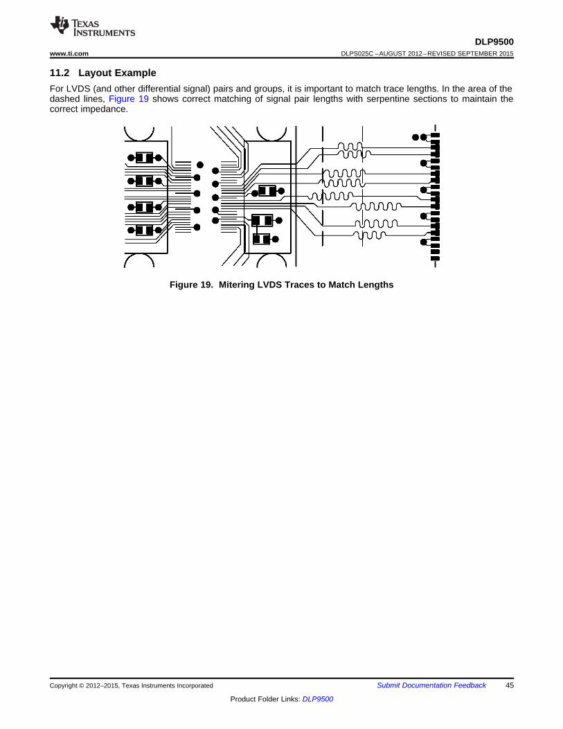
DLP9500www.ti.com DLPS025C –AUGUST 2012–REVISED SEPTEMBER 2015
11.2 Layout ExampleFor LVDS (and other differential signal) pairs and groups, it is important to match trace lengths. In the area of thedashed lines, Figure 19 shows correct matching of signal pair lengths with serpentine sections to maintain thecorrect impedance.
Figure 19. Mitering LVDS Traces to Match Lengths
Copyright © 2012–2015, Texas Instruments Incorporated Submit Documentation Feedback 45
Product Folder Links: DLP9500
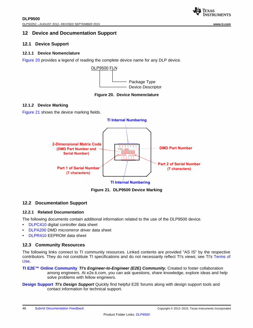
TI Internal Numbering
2-Dimensional Matrix Code
(DMD Part Number and
Serial Number)
Part 1 of Serial Number
(7 characters)
TI Internal Numbering
Part 2 of Serial Number
(7 characters)
DMD Part Number
DLP9500 FLN
Package TypeDevice Descriptor
DLP9500DLPS025C –AUGUST 2012–REVISED SEPTEMBER 2015 www.ti.com
12 Device and Documentation Support
12.1 Device Support
12.1.1 Device NomenclatureFigure 20 provides a legend of reading the complete device name for any DLP device.
Figure 20. Device Nomenclature
12.1.2 Device MarkingFigure 21 shows the device marking fields.
Figure 21. DLP9500 Device Marking
12.2 Documentation Support
12.2.1 Related DocumentationThe following documents contain additional information related to the use of the DLP9500 device.• DLPC410 digital controller data sheet• DLPA200 DMD micromirror driver data sheet• DLPR410 EEPROM data sheet
12.3 Community ResourcesThe following links connect to TI community resources. Linked contents are provided "AS IS" by the respectivecontributors. They do not constitute TI specifications and do not necessarily reflect TI's views; see TI's Terms ofUse.
TI E2E™ Online Community TI's Engineer-to-Engineer (E2E) Community. Created to foster collaborationamong engineers. At e2e.ti.com, you can ask questions, share knowledge, explore ideas and helpsolve problems with fellow engineers.
Design Support TI's Design Support Quickly find helpful E2E forums along with design support tools andcontact information for technical support.
46 Submit Documentation Feedback Copyright © 2012–2015, Texas Instruments Incorporated
Product Folder Links: DLP9500
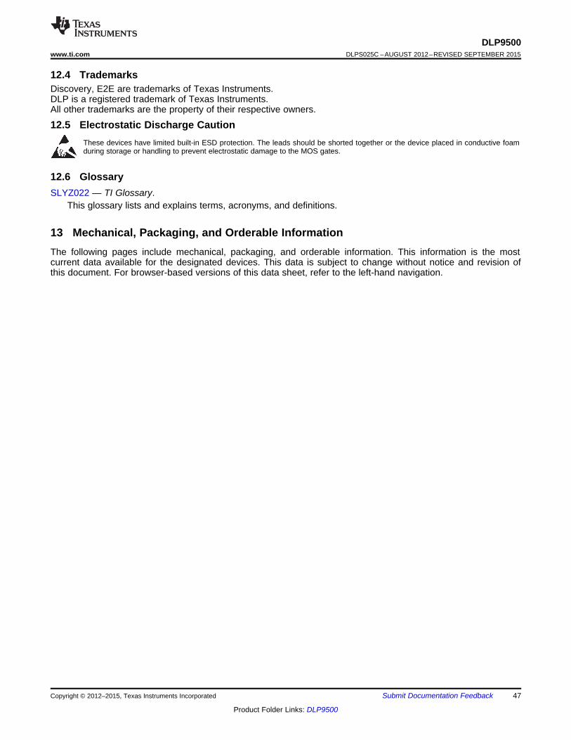
DLP9500www.ti.com DLPS025C –AUGUST 2012–REVISED SEPTEMBER 2015
12.4 TrademarksDiscovery, E2E are trademarks of Texas Instruments.DLP is a registered trademark of Texas Instruments.All other trademarks are the property of their respective owners.
12.5 Electrostatic Discharge CautionThese devices have limited built-in ESD protection. The leads should be shorted together or the device placed in conductive foamduring storage or handling to prevent electrostatic damage to the MOS gates.
12.6 GlossarySLYZ022 — TI Glossary.
This glossary lists and explains terms, acronyms, and definitions.
13 Mechanical, Packaging, and Orderable InformationThe following pages include mechanical, packaging, and orderable information. This information is the mostcurrent data available for the designated devices. This data is subject to change without notice and revision ofthis document. For browser-based versions of this data sheet, refer to the left-hand navigation.
Copyright © 2012–2015, Texas Instruments Incorporated Submit Documentation Feedback 47
Product Folder Links: DLP9500
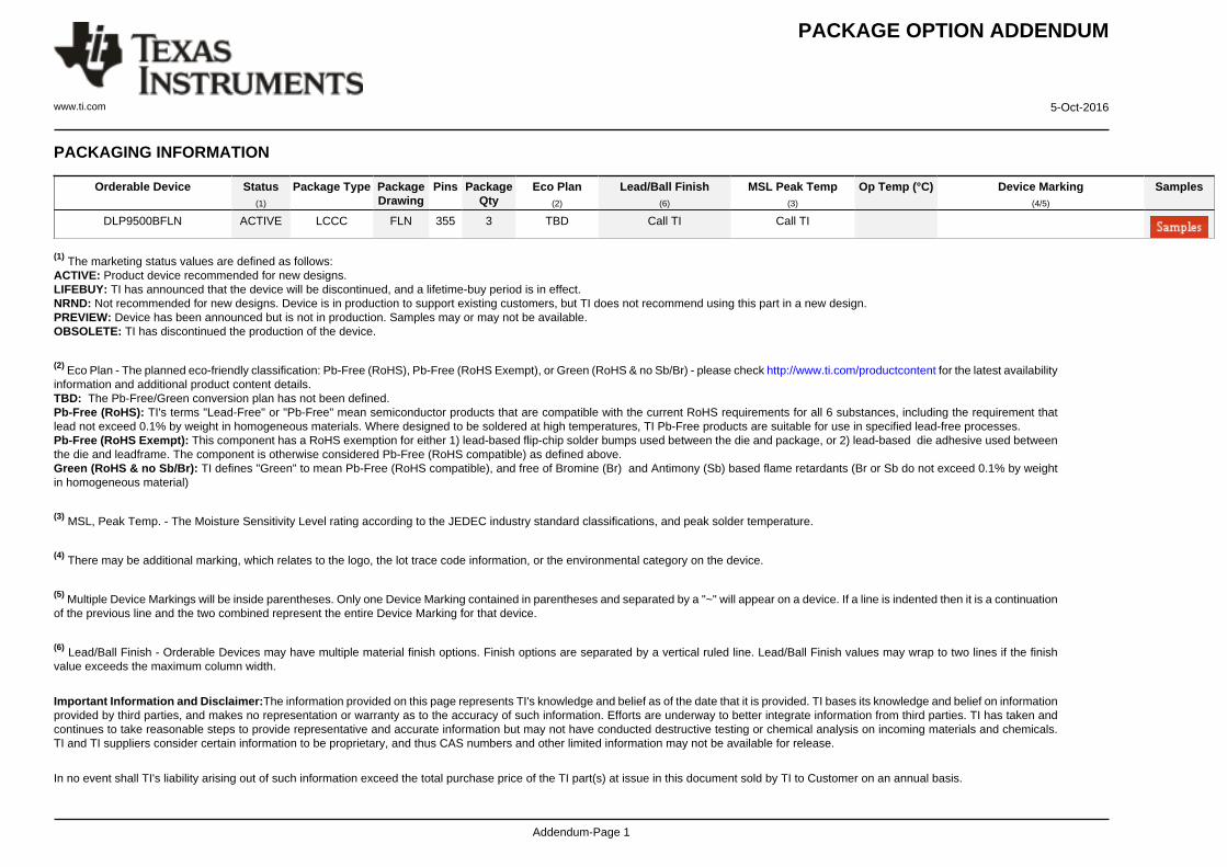
PACKAGE OPTION ADDENDUM
www.ti.com 5-Oct-2016
Addendum-Page 1
PACKAGING INFORMATION
Orderable Device Status(1)
Package Type PackageDrawing
Pins PackageQty
Eco Plan(2)
Lead/Ball Finish(6)
MSL Peak Temp(3)
Op Temp (°C) Device Marking(4/5)
Samples
DLP9500BFLN ACTIVE LCCC FLN 355 3 TBD Call TI Call TI
(1) The marketing status values are defined as follows:ACTIVE: Product device recommended for new designs.LIFEBUY: TI has announced that the device will be discontinued, and a lifetime-buy period is in effect.NRND: Not recommended for new designs. Device is in production to support existing customers, but TI does not recommend using this part in a new design.PREVIEW: Device has been announced but is not in production. Samples may or may not be available.OBSOLETE: TI has discontinued the production of the device.
(2) Eco Plan - The planned eco-friendly classification: Pb-Free (RoHS), Pb-Free (RoHS Exempt), or Green (RoHS & no Sb/Br) - please check http://www.ti.com/productcontent for the latest availabilityinformation and additional product content details.TBD: The Pb-Free/Green conversion plan has not been defined.Pb-Free (RoHS): TI's terms "Lead-Free" or "Pb-Free" mean semiconductor products that are compatible with the current RoHS requirements for all 6 substances, including the requirement thatlead not exceed 0.1% by weight in homogeneous materials. Where designed to be soldered at high temperatures, TI Pb-Free products are suitable for use in specified lead-free processes.Pb-Free (RoHS Exempt): This component has a RoHS exemption for either 1) lead-based flip-chip solder bumps used between the die and package, or 2) lead-based die adhesive used betweenthe die and leadframe. The component is otherwise considered Pb-Free (RoHS compatible) as defined above.Green (RoHS & no Sb/Br): TI defines "Green" to mean Pb-Free (RoHS compatible), and free of Bromine (Br) and Antimony (Sb) based flame retardants (Br or Sb do not exceed 0.1% by weightin homogeneous material)
(3) MSL, Peak Temp. - The Moisture Sensitivity Level rating according to the JEDEC industry standard classifications, and peak solder temperature.
(4) There may be additional marking, which relates to the logo, the lot trace code information, or the environmental category on the device.
(5) Multiple Device Markings will be inside parentheses. Only one Device Marking contained in parentheses and separated by a "~" will appear on a device. If a line is indented then it is a continuationof the previous line and the two combined represent the entire Device Marking for that device.
(6) Lead/Ball Finish - Orderable Devices may have multiple material finish options. Finish options are separated by a vertical ruled line. Lead/Ball Finish values may wrap to two lines if the finishvalue exceeds the maximum column width.
Important Information and Disclaimer:The information provided on this page represents TI's knowledge and belief as of the date that it is provided. TI bases its knowledge and belief on informationprovided by third parties, and makes no representation or warranty as to the accuracy of such information. Efforts are underway to better integrate information from third parties. TI has taken andcontinues to take reasonable steps to provide representative and accurate information but may not have conducted destructive testing or chemical analysis on incoming materials and chemicals.TI and TI suppliers consider certain information to be proprietary, and thus CAS numbers and other limited information may not be available for release.
In no event shall TI's liability arising out of such information exceed the total purchase price of the TI part(s) at issue in this document sold by TI to Customer on an annual basis.
PACKAGE OPTION ADDENDUM
www.ti.com 5-Oct-2016
Addendum-Page 2
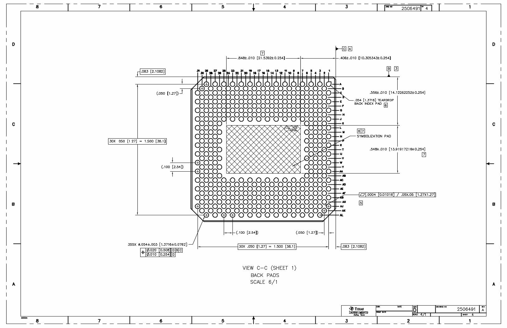

IMPORTANT NOTICE
Texas Instruments Incorporated and its subsidiaries (TI) reserve the right to make corrections, enhancements, improvements and otherchanges to its semiconductor products and services per JESD46, latest issue, and to discontinue any product or service per JESD48, latestissue. Buyers should obtain the latest relevant information before placing orders and should verify that such information is current andcomplete. All semiconductor products (also referred to herein as “components”) are sold subject to TI’s terms and conditions of salesupplied at the time of order acknowledgment.TI warrants performance of its components to the specifications applicable at the time of sale, in accordance with the warranty in TI’s termsand conditions of sale of semiconductor products. Testing and other quality control techniques are used to the extent TI deems necessaryto support this warranty. Except where mandated by applicable law, testing of all parameters of each component is not necessarilyperformed.TI assumes no liability for applications assistance or the design of Buyers’ products. Buyers are responsible for their products andapplications using TI components. To minimize the risks associated with Buyers’ products and applications, Buyers should provideadequate design and operating safeguards.TI does not warrant or represent that any license, either express or implied, is granted under any patent right, copyright, mask work right, orother intellectual property right relating to any combination, machine, or process in which TI components or services are used. Informationpublished by TI regarding third-party products or services does not constitute a license to use such products or services or a warranty orendorsement thereof. Use of such information may require a license from a third party under the patents or other intellectual property of thethird party, or a license from TI under the patents or other intellectual property of TI.Reproduction of significant portions of TI information in TI data books or data sheets is permissible only if reproduction is without alterationand is accompanied by all associated warranties, conditions, limitations, and notices. TI is not responsible or liable for such altereddocumentation. Information of third parties may be subject to additional restrictions.Resale of TI components or services with statements different from or beyond the parameters stated by TI for that component or servicevoids all express and any implied warranties for the associated TI component or service and is an unfair and deceptive business practice.TI is not responsible or liable for any such statements.Buyer acknowledges and agrees that it is solely responsible for compliance with all legal, regulatory and safety-related requirementsconcerning its products, and any use of TI components in its applications, notwithstanding any applications-related information or supportthat may be provided by TI. Buyer represents and agrees that it has all the necessary expertise to create and implement safeguards whichanticipate dangerous consequences of failures, monitor failures and their consequences, lessen the likelihood of failures that might causeharm and take appropriate remedial actions. Buyer will fully indemnify TI and its representatives against any damages arising out of the useof any TI components in safety-critical applications.In some cases, TI components may be promoted specifically to facilitate safety-related applications. With such components, TI’s goal is tohelp enable customers to design and create their own end-product solutions that meet applicable functional safety standards andrequirements. Nonetheless, such components are subject to these terms.No TI components are authorized for use in FDA Class III (or similar life-critical medical equipment) unless authorized officers of the partieshave executed a special agreement specifically governing such use.Only those TI components which TI has specifically designated as military grade or “enhanced plastic” are designed and intended for use inmilitary/aerospace applications or environments. Buyer acknowledges and agrees that any military or aerospace use of TI componentswhich have not been so designated is solely at the Buyer's risk, and that Buyer is solely responsible for compliance with all legal andregulatory requirements in connection with such use.TI has specifically designated certain components as meeting ISO/TS16949 requirements, mainly for automotive use. In any case of use ofnon-designated products, TI will not be responsible for any failure to meet ISO/TS16949.
Products ApplicationsAudio www.ti.com/audio Automotive and Transportation www.ti.com/automotiveAmplifiers amplifier.ti.com Communications and Telecom www.ti.com/communicationsData Converters dataconverter.ti.com Computers and Peripherals www.ti.com/computersDLP® Products www.dlp.com Consumer Electronics www.ti.com/consumer-appsDSP dsp.ti.com Energy and Lighting www.ti.com/energyClocks and Timers www.ti.com/clocks Industrial www.ti.com/industrialInterface interface.ti.com Medical www.ti.com/medicalLogic logic.ti.com Security www.ti.com/securityPower Mgmt power.ti.com Space, Avionics and Defense www.ti.com/space-avionics-defenseMicrocontrollers microcontroller.ti.com Video and Imaging www.ti.com/videoRFID www.ti-rfid.comOMAP Applications Processors www.ti.com/omap TI E2E Community e2e.ti.comWireless Connectivity www.ti.com/wirelessconnectivity
Mailing Address: Texas Instruments, Post Office Box 655303, Dallas, Texas 75265Copyright © 2016, Texas Instruments Incorporated