Development Board EPC9126 Quick Start Guide - epc...
7
Development Board EPC9126 Quick Start Guide EPC2016C 100 V High Current Pulsed Laser Diode Driver Revision 2.5
Transcript of Development Board EPC9126 Quick Start Guide - epc...
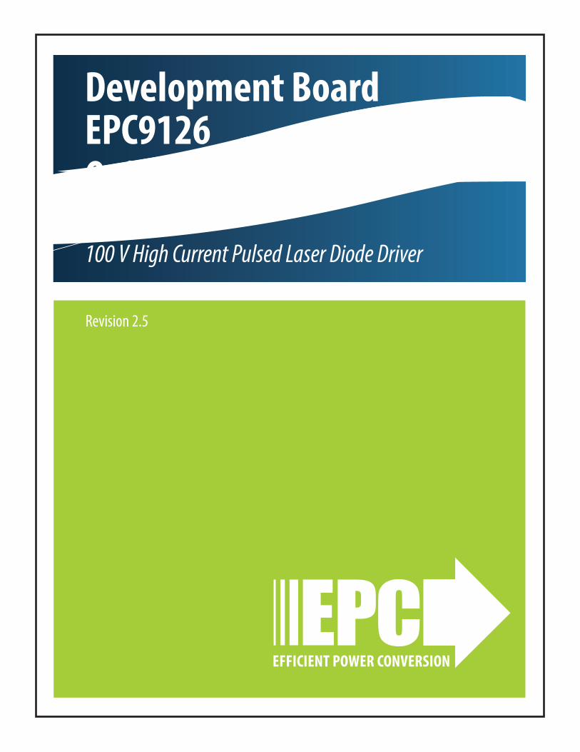
Development Board EPC9126Quick Start GuideEPC2016C 100 V High Current Pulsed Laser Diode Driver
Revision 2.5
QUICK START GUIDE Demonstration System EPC9126
2 | | EPC – EFFICIENT POWER CONVERSION CORPORATION | WWW.EPC-CO.COM | COPYRIGHT 2017
DESCRIPTION The EPC9126 development board is primarily intended to drive laser diodes with high current pulses with total pulse widths as low as 5 ns (10% of peak). The board is shipped with an EPC2016C enhancement mode (eGaN®) field effect transistor (FET), a 100 V maximum device voltage capable of current pulses up to 75 A. The board does not include a laser diode, which must be supplied by the user.
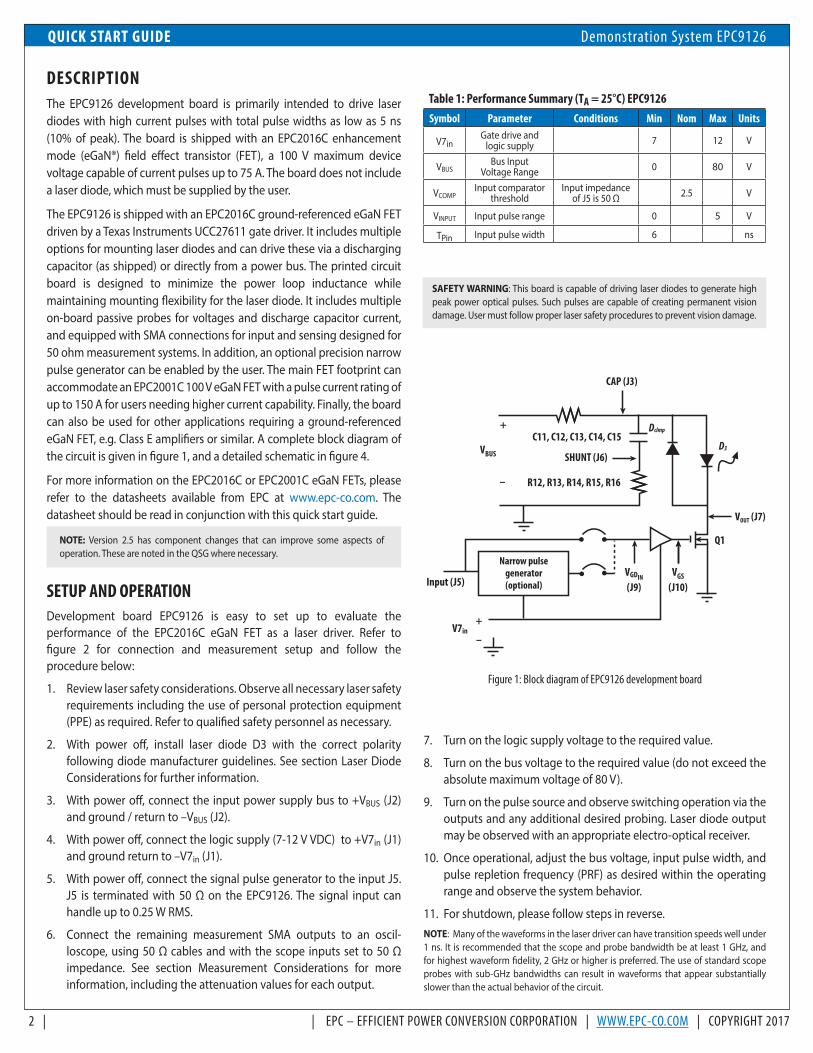
The EPC9126 is shipped with an EPC2016C ground-referenced eGaN FET driven by a Texas Instruments UCC27611 gate driver. It includes multiple options for mounting laser diodes and can drive these via a discharging capacitor (as shipped) or directly from a power bus. The printed circuit board is designed to minimize the power loop inductance while maintaining mounting flexibility for the laser diode. It includes multiple on-board passive probes for voltages and discharge capacitor current, and equipped with SMA connections for input and sensing designed for 50 ohm measurement systems. In addition, an optional precision narrow pulse generator can be enabled by the user. The main FET footprint can accommodate an EPC2001C 100 V eGaN FET with a pulse current rating of up to 150 A for users needing higher current capability. Finally, the board can also be used for other applications requiring a ground-referenced eGaN FET, e.g. Class E amplifiers or similar. A complete block diagram of the circuit is given in figure 1, and a detailed schematic in figure 4.
For more information on the EPC2016C or EPC2001C eGaN FETs, please refer to the datasheets available from EPC at www.epc-co.com. The datasheet should be read in conjunction with this quick start guide.
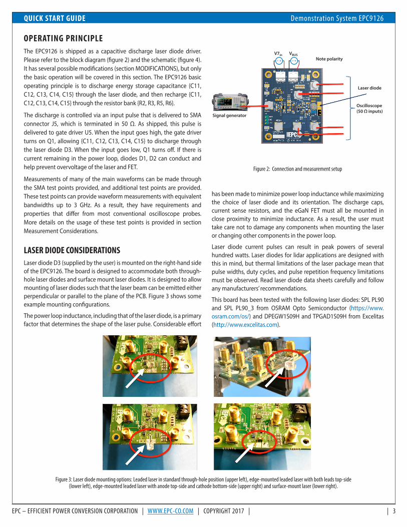
SETUP AND OPERATION Development board EPC9126 is easy to set up to evaluate the performance of the EPC2016C eGaN FET as a laser driver. Refer to figure 2 for connection and measurement setup and follow the procedure below:
1. Review laser safety considerations. Observe all necessary laser safety requirements including the use of personal protection equipment (PPE) as required. Refer to qualified safety personnel as necessary.
2. With power off, install laser diode D3 with the correct polarity following diode manufacturer guidelines. See section Laser Diode Considerations for further information.
3. With power off, connect the input power supply bus to +VBUS (J2) and ground / return to –VBUS (J2).
4. With power off, connect the logic supply (7-12 V VDC) to +V7in (J1) and ground return to –V7in (J1).
5. With power off, connect the signal pulse generator to the input J5. J5 is terminated with 50 Ω on the EPC9126. The signal input can handle up to 0.25 W RMS.
6. Connect the remaining measurement SMA outputs to an oscil-loscope, using 50 Ω cables and with the scope inputs set to 50 Ω impedance. See section Measurement Considerations for more information, including the attenuation values for each output.
Table 1: Performance Summary (TA = 25°C) EPC9126 Symbol Parameter Conditions Min Nom Max Units
V7inGate drive and
logic supply 7 12 V
VBUSBus Input
Voltage Range 0 80 V
VCOMPInput comparator
thresholdInput impedance
of J5 is 50 Ω 2.5 V
VINPUT Input pulse range 0 5 V
TPin Input pulse width 6 ns
7. Turn on the logic supply voltage to the required value.
8. Turn on the bus voltage to the required value (do not exceed the absolute maximum voltage of 80 V).
9. Turn on the pulse source and observe switching operation via the outputs and any additional desired probing. Laser diode output may be observed with an appropriate electro-optical receiver.
10. Once operational, adjust the bus voltage, input pulse width, and pulse repletion frequency (PRF) as desired within the operating range and observe the system behavior.
11. For shutdown, please follow steps in reverse.NOTE: Many of the waveforms in the laser driver can have transition speeds well under 1 ns. It is recommended that the scope and probe bandwidth be at least 1 GHz, and for highest waveform fidelity, 2 GHz or higher is preferred. The use of standard scope probes with sub-GHz bandwidths can result in waveforms that appear substantially slower than the actual behavior of the circuit.
SAFETY WARNING: This board is capable of driving laser diodes to generate high peak power optical pulses. Such pulses are capable of creating permanent vision damage. User must follow proper laser safety procedures to prevent vision damage.
Figure 1: Block diagram of EPC9126 development board
CAP (J3)
VOUT (J7)
Q1
VGS
(J10)VGDIN
(J9)Input (J5)
VBUS
C11, C12, C13, C14, C15
R12, R13, R14, R15, R16
SHUNT (J6)
V7in+
+
–
–
Narrow pulsegenerator(optional)
Dclmp
D3
NOTE: Version 2.5 has component changes that can improve some aspects of operation. These are noted in the QSG where necessary.
QUICK START GUIDE Demonstration System EPC9126
EPC – EFFICIENT POWER CONVERSION CORPORATION | WWW.EPC-CO.COM | COPYRIGHT 2017 | | 3
Figure 2: Connection and measurement setup
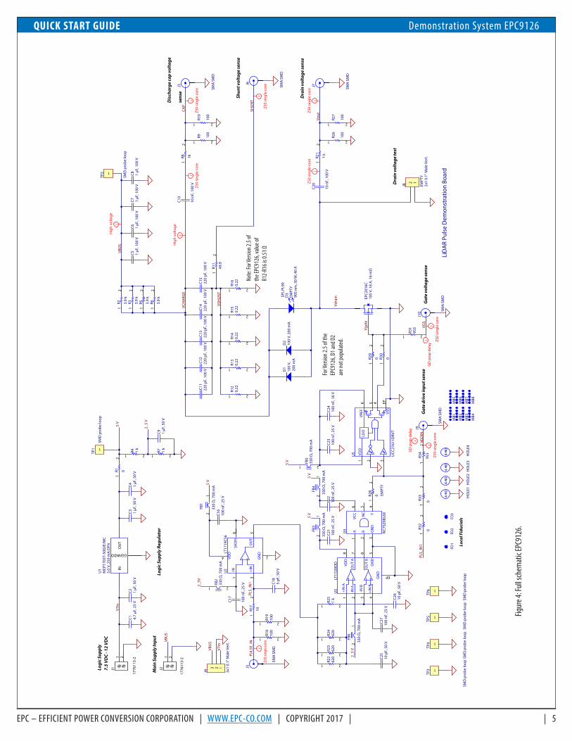
OPERATING PRINCIPLE The EPC9126 is shipped as a capacitive discharge laser diode driver. Please refer to the block diagram (figure 2) and the schematic (figure 4). It has several possible modifications (section MODIFICATIONS), but only the basic operation will be covered in this section. The EPC9126 basic operating principle is to discharge energy storage capacitance {C11, C12, C13, C14, C15} through the laser diode, and then recharge {C11, C12, C13, C14, C15} through the resistor bank {R2, R3, R5, R6}.
The discharge is controlled via an input pulse that is delivered to SMA connector J5, which is terminated in 50 Ω. As shipped, this pulse is delivered to gate driver U5. When the input goes high, the gate driver turns on Q1, allowing {C11, C12, C13, C14, C15} to discharge through the laser diode D3. When the input goes low, Q1 turns off. If there is current remaining in the power loop, diodes D1, D2 can conduct and help prevent overvoltage of the laser and FET.
Measurements of many of the main waveforms can be made through the SMA test points provided, and additional test points are provided. These test points can provide waveform measurements with equivalent bandwidths up to 3 GHz. As a result, they have requirements and properties that differ from most conventional oscilloscope probes. More details on the usage of these test points is provided in section Measurement Considerations.
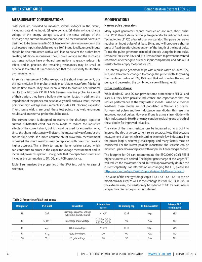
LASER DIODE CONSIDERATIONS Laser diode D3 (supplied by the user) is mounted on the right-hand side of the EPC9126. The board is designed to accommodate both through-hole laser diodes and surface mount laser diodes. It is designed to allow mounting of laser diodes such that the laser beam can be emitted either perpendicular or parallel to the plane of the PCB. Figure 3 shows some example mounting configurations.
The power loop inductance, including that of the laser diode, is a primary factor that determines the shape of the laser pulse. Considerable effort
has been made to minimize power loop inductance while maximizing the choice of laser diode and its orientation. The discharge caps, current sense resistors, and the eGaN FET must all be mounted in close proximity to minimize inductance. As a result, the user must take care not to damage any components when mounting the laser or changing other components in the power loop.
Laser diode current pulses can result in peak powers of several hundred watts. Laser diodes for lidar applications are designed with this in mind, but thermal limitations of the laser package mean that pulse widths, duty cycles, and pulse repetition frequency limitations must be observed. Read laser diode data sheets carefully and follow any manufacturers’ recommendations.
This board has been tested with the following laser diodes: SPL PL90 and SPL PL90_3 from OSRAM Opto Semiconductor (https://www.osram.com/os/) and DPEGW1S09H and TPGAD1S09H from Excelitas (http://www.excelitas.com).
Laser diode
V7in VBUSNote polarity
Signal generator
Oscilloscope(50 Ω inputs)
– + +–
Figure 3: Laser diode mounting options: Leaded laser in standard through-hole position (upper left), edge-mounted leaded laser with both leads top-side (lower left), edge-mounted leaded laser with anode top-side and cathode bottom-side (upper right) and surface-mount laser (lower right).
QUICK START GUIDE Demonstration System EPC9126
4 | | EPC – EFFICIENT POWER CONVERSION CORPORATION | WWW.EPC-CO.COM | COPYRIGHT 2017
MEASUREMENT CONSIDERATIONSSMA jacks are provided to measure several voltages in the circuit, including gate drive input, Q1 gate voltage, Q1 drain voltage, charge voltage of the energy storage cap, and the sense voltage of the discharge cap current measurement shunt. All measurement points are designed to be terminated in 50 Ω, hence when viewing waveforms, the oscilloscope inputs should be set to a 50 Ω input. Ideally, unused inputs should be also terminated with a 50 Ω load to prevent the probes from creating additional resonances. The Q1 drain voltage and the discharge cap sense voltage have on-board terminations to greatly reduce this effect, and in practice, the remaining resonances may be small or otherwise tolerable. It is recommended that the user verify this for their own requirements.
All sense measurement SMAs, except for the shunt measurement, use the transmission line probe principle to obtain waveform fidelity at sub-ns time scales. They have been verified to produce near-identical results to a Tektronix P9158 3 GHz transmission line probe. As a result of their design, they have a built-in attenuation factor. In addition, the impedance of the probes can be relatively small, and as a result, the test points for high voltage measurements include a DC blocking capacitor. If long pulse widths are used, these test points may yield erroneous results, and an external probe should be used.
The current shunt is designed to estimate the discharge capacitor current. Substantial effort has been made to reduce the inductive effects of the current shunt, but it should be used for estimation only, since the shunt inductance will distort the measured waveforms at the sub-ns time scale. If a more accurate shunt waveform measurement is desired, the shunt resistors may be replaced with ones that provide higher accuracy. This is likely to require higher resistor values, which can contribute to errors in the capacitor voltage measurement and in increased power dissipation. Finally, note that the capacitor current also includes the current due to D1, D2, and PCB capacitance.
Table 2 summarizes the properties of the SMA test points for ease of reference.
MODIFICATIONS Narrow pulse generator:
Many signal generators cannot produce an accurate, short pulse. The EPC9126 includes a narrow pulse generator based on the Linear Technologies LT1720 ultrafast dual comparator. This pulse generator requires an input pulse of at least 20 ns, and will produce a shorter pulse of fixed duration, independent of the length of the input pulse. To use the pulse generator instead of directly using the input pulse, remove 0 Ω resistors R32 and R33 (remove both to prevent unwanted reflections at either gate driver or input comparator), and add a 0 Ω resistor to the empty footprint for R28.
The internal pulse generator ships with a pulse width of ~8 ns. R22, R23, and R24 can be changed to change the pulse width. Increasing the combined value of R22, R23, and R24 will shorten the output pulse, and decreasing the combined value will lengthen it.
Other modifications:
While diodes D1 and D2 can provide some protection to FET Q1 and laser D3, they have parasitic inductance and capacitance that can reduce performance at the very fastest speeds. Based on customer feedback, these diodes are not populated in Version 2.5 boards. For very fast pulses and low inductance laser diodes, this results in improved optical pulses. However, if one is using a laser diode with high inductance (>10 nH), one may consider replacing one or both of these diodes for improved reliability.
The value of the shunt resistors can be increased up to a point to improve the discharge cap current sense accuracy. Note that accurate measurement of current while inserting extremely low inductance into the power loop is extremely challenging, and many factors must be considered. For the lowest possible inductance, the resistors can be mounted upside down or replaced with copper foil if no sensing is needed.
The footprint for Q1 can accommodate the EPC2001C eGaN FET if higher currents are desired. The higher gate charge of the larger FET will reduce the maximum speed, but will approximately double the current capability. For information on changing the FET, please see http://epc-co.com/epc/DesignSupport/AssemblyResources.aspx.
The value of the energy storage cap {C11, C12, C13, C14, C15} can be modified as desired, as well as the recharge resistor {R2, R3, R5, R6}. In the extreme case, the resistor may be reduced to 0 Ω for cases where a capacitive discharge pulse is not desired.
Table 2: Properties of SMA test points
Designator PCB label Description Attenuation factor DC blocking cap LF time constant Internal 50 Ω
termination
J3 CAP Discharge capacitor voltage (VCHARGE on schematic) 41 V/V 10 nF 10 μs YES
J6 SHUNT Discharge shunt voltage 22.7 A/V (V2.0)9.80 A/V (V2.5) NO N/A NO
J7 VOUT Q1 drain voltage 41 V/V 10 nF 10 μs YES
J9 VGDINGate drive input 20 NO N/A NO
J10 VGS Q1 gate voltage 20 NO N/A NO
QUICK START GUIDE Demonstration System EPC9126
EPC – EFFICIENT POWER CONVERSION CORPORATION | WWW.EPC-CO.COM | COPYRIGHT 2017 | | 5
Figur
e 4: F
ull sc
hem
atic
EPC9
126.
LiD
AR
Puls
e D
emon
stra
tion
Boar
d
5 V
7.5
VDC
- 12
VDC
Logi
c Sup
ply
Regu
lato
r
MCP
1703
T-50
02E/
MC
5.0
V, 2
50 m
A D
FN OU
TIN
GGNNDD
U1
Logi
c Sup
ply
Mai
n Su
pply
Inpu
t
V7in
PULS
E_IN
SMA
SM
D
J5
SMA
SM
D
J7
100
1 2R18
0.22
1 2
R12
100
1 2
R26
Vout
5 V
1 µF
, 50
VC2
1 µF
, 50
VC3
1 µF
, 50
VC4
2x1
0.1"
Mal
e Ve
rt.
12
J8 EMPT
Y
VBU
S
100
1 2R19
100
1 2
R27
100
nF, 2
5 V
C23
02
1 R1
Vdra
in
Vgat
e
SMD
pro
be lo
op
1
TP2
SMD
pro
be lo
op
1
TP4
SMD
pro
be lo
op
1
TP1
VBU
S
VCH
ARG
E
SMD
pro
be lo
op
1
TP3
5 pF
, 50
VC1
8
102
1 R1
7
16 5 4
32
VCC
GN
D
A B
YNC
U4
NC7
SZ08
L6X
10 p
F, 5
0 V
C25
10 p
F, 5
0 V
C26
100
nF, 2
5 V
C27
0
21
R32
02
1 R2
8
EMPT
Y
1
5
4
3
2
VDD
GN
D
OU
T+I
N
-IN6
SHD
N
U2
LT17
19CS
6
1
6 5432
VDD
GN
D
OU
T A
OU
T B
+IN
A
78
EP
-IN A
+IN
B
-IN B
GN
D
U3
LT17
20ID
D10
0 nF
, 25
VC2
210
0 nF
, 25
VC2
1
100
nF, 2
5 V
C16
5 V
1 µF
, 50
VC9
2_5
V
2_5V
2_5
V
100
nF, 2
5 V
C17
PLS_
IN1
PLS_
IN1
620
1 2R22
1 k
1 2R4 1 k
1 2R7
1 k
1 2R25
620
1 2R23
620
1 2R24
100
V, 1
8 A
, 16
mΩ
EPC2
016C
220
pF, 1
00 V
C11
220
pF, 1
00 V
C12
220
pF, 1
00 V
C13
220
pF, 1
00 V
C14
220
pF, 1
00 V
C15
3.9
k2
1 R2 3.
9 k
21
R3 3.9
k2
1 R5 3.
9 k
21
R6
6
2 3EP45
LDO
VREF VS
S
1 VD
D
U5
UCC
2761
1DRV
T
VSH
UN
T
1 µF
, 100
VC5
1 µF
, 100
VC6
1 µF
, 100
VC7
1 µF
, 100
VC8
330
Ω, 7
00 m
A1
2
FB1
330
Ω, 7
00 m
A12
FB3
330
Ω, 7
00 m
A1
2FB
4
100
nF, 1
6 V
C24
10 n
F, 1
00 V
C20
953
1 R3
42
VGD
INVG
S
1 k
21
R21
Gat
e dr
ive
inpu
t sen
se
SMA
SM
D
J3
100
1 2
R9
100
1 2
R10
10 n
F, 1
00 V
C10
1k2
1 R8
SMA
SM
D
J6
SMA
SM
D
J10
SMA
SM
D
J995
3
1 2R31
49.9
21
R11
02
1 R2
9
02
1 R3
0
Gat
e vo
ltage
sens
e
Shun
t vol
tage
sens
e
Dis
char
ge ca
p vo
ltage
sens
e
Dra
in v
olta
ge te
st
4.7
µF, 2
5 V
C1
330
Ω, 7
00 m
A1
2FB
6
330
Ω, 7
00 m
A
1 2FB2
4-40
HO
LE1
4-40
HO
LE2
4-40
HO
LE3
4-40
HO
LE4
SPL
PL90
905
nm, 3
0 W
, 40
A
D3
EMPT
Y
1 2
J1
1776
113-
2
0
21
R33
330
Ω, 7
00 m
A
1 2FB5
CAP
SHU
NT
iZ5
0 sin
gle
core
iZ5
0 si
ngle
cor
ei
Z50
sing
le c
ore
iZ5
0 si
ngle
cor
e
iZ5
0 si
ngle
cor
e
iZ5
0 si
ngle
cor
e
iG
D p
rop
dela
y
GD
pro
p de
lay
i
SMD
pro
be lo
op
1
TP6
SMD
pro
be lo
op
1
TP5
3x1
0.1"
Mal
e Ve
rt.
123
J4
V7in
VBU
S
iZ5
0 si
ngle
cor
e
iZ5
0 si
ngle
cor
e
0.22
1 2
R13
0.22
1 2
R14
0.22
1 2
R15
0.22
1 2
R16
iH
igh
volta
ge
iH
igh
volta
ge
5 V
5 V
1 2
J2
1776
113-
2
100
V, 2
00 m
A
D1
100
V, 2
00 m
AD
2
Dra
in v
olta
ge se
nse
FD1 Lo
cal F
iduc
ials
FD2
FD3
MB1
MB2
MB3
MB4
MB5
MB6
MB7
MB8
Note
: For
Versi
on 2.
5 of
the E
PC91
26, v
alue o
f R1
2-R1
6 is 0
.51 Ω
For V
ersio
n 2.5
of th
e EP
C912
6, D1
and D
2 ar
e not
popu
lated
.
QUICK START GUIDE Demonstration System EPC9126
6 | | EPC – EFFICIENT POWER CONVERSION CORPORATION | WWW.EPC-CO.COM | COPYRIGHT 2017
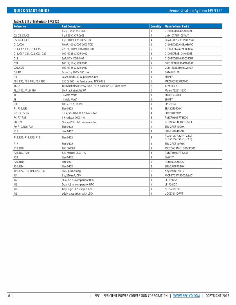
Table 3: Bill of Materials - EPC9126Reference Part Description Quantity Manufacturer Part #C1 4.7 µF, 25 V, X5R 0603 1 C1608X5R1E475K080ACC2, C3, C4, C9 1 µF, 25 V, X7R 0603 4 UMK107AB7105KA-TC5, C6, C7, C8 1 µF, 100 V, X7S 0805 TDK 4 CGA4J3X7S2A105K125AEC10, C20 10 nF, 100 V, C0G 0603 TDK 2 C1608C0G2A103J080ACC11, C12, C13, C14, C15 220 pF, 100 V, C0G 0402 TDK 5 C1005C0G2A221J050BAC16, C17, C21, C22, C23, C27 100 nF, 25 V, X7R 0402 6 C1005X7R1E104K050BB
C18 5pF, 50 V, C0G 0402 1 C1005C0G1H050C050BA
C24 100 nF, 16 V, X7R 0306 1 C0816X7R1C104M050ACC25, C26 100 nF, 25 V, X7R 0402 2 GCM1885C1H100JA16DD1, D2 Schottky 100 V, 200 mA 2 BAT41KFILMD3 Laser diode, 30 W, peak 905 nm 1 EMPTYFB1, FB2, FB3, FB4, FB5, FB6 330 Ω, 700 mA, ferrite bead TDK 0402 6 MPZ1005S331ET000J1, J2 Terminal block screw type THT 2-position 3.81 mm pitch 2 1776113-2J3, J5, J6, J7, J9, J10 SMA jack straight SM 6 Molex 73251-1350J4 .1 Male Vert." 1 68001-236HLFJ8 .1 Male Vert." 1 EMPTYQ1 100 V, 18 A, 16 mΩ 1 EPC2016CR1, R32, R33 Size 0402 3 ERJ-2GE0R00XR2, R3, R5, R6 3.9 k, 5%, 0.67 W, 1206 resistor 4 ERJ-P08J392VR4, R7, R25 1 k resistor 0603 1% 3 RMCF0603FT1K00R8, R21 Vishay PHP 0603 wide resistor 2 PHP00603E1001BST1R9, R10, R26, R27 Size 0402 4 ERJ-2RKF1000XR11 Size 0402 1 ERJ-2RKF49R9X
R12, R13, R14, R15, R16 Size 0402 5 RL0510S-R22-F (V2.0) RL0510S-R51-F (V2.5)
R17 Size 0402 1 ERJ-2RKF10R0XR18, R19 100 Ω 0603 2 MCT0603MC1000FP500R22, R23, R24 620 resistor 0603 1% 3 RMCF0603FT620RR28 Size 0402 1 EMPTYR29, R30 Size 0201 2 RC0603J000CSR31, R34 Size 0402 2 ERJ-2RKF9530XTP1, TP2, TP3, TP4, TP5, TP6 SMD probe loop 6 Keystone, 5015 U1 5 V, 250 mA, DFN 1 MCP1703T-5002E/MC U2 Dual 4.5 ns comparator RRO 1 LT1719CS6 U3 Dual 4.5 ns comparator RRO 1 LT1720IDD U4 TinyLogic UHS 2 input AND 1 NC7SZ08L6X U5 eGaN gate driver with LDO 1 UCC27611DRVT

Demonstration Board Notification
The EPC9126 board is intended for product evaluation purposes only and is not intended for commercial use. Replace components on the Evaluation Board only with those parts shown on the parts list (or Bill of Materials) in the Quick Start Guide. Contact an authorized EPC representative with any questions.This board is intended to be used by certified professionals, in a lab environment, following proper safety procedures. Use at your own risk. As an evaluation tool, this board is not designed for compliance with the European Union directive on electromagnetic compatibility or any other such directives or regulations. As board builds are at times subject to product availability, it is possible that boards may contain components or assembly materials that are not RoHS compliant. Efficient Power Conversion Corporation (EPC) makes no guarantee that the purchased board is 100% RoHS compliant.The Evaluation board (or kit) is for demonstration purposes only and neither the Board nor this Quick Start Guide constitute a sales contract or create any kind of warranty, whether express or implied, as to the applications or products involved. Disclaimer: EPC reserves the right at any time, without notice, to make changes to any products described herein to improve reliability, function, or design. EPC does not assume any liability arising out of the application or use of any product or circuit described herein; neither does it convey any license under its patent rights, or other intellectual property whatsoever, nor the rights of others.
EPC Products are distributed through Digi-Key.www.digikey.com
For More Information:
Please contact [email protected] your local sales representative
Visit our website: www.epc-co.com
Sign-up to receive EPC updates atbit.ly/EPCupdates or text “EPC” to 22828