
DesignandComparisonof24GHzPatchAntennason ...downloads.hindawi.com/archive/2010/535307.pdf · s...
10
Hindawi Publishing Corporation International Journal of Microwave Science and Technology Volume 2010, Article ID 535307, 9 pages doi:10.1155/2010/535307 Research Article Design and Comparison of 24 GHz Patch Antennas on Glass Substrates for Compact Wireless Sensor Nodes Florian Ohnimus, 1 Uwe Maaß, 2 Gerhard Fotheringham, 2 Brian Curran, 2 Ivan Ndip, 2 Thomas Fritzsch, 2 J¨ urgen Wolf, 2 Stephan Guttowski, 2 and Klaus-Dieter Lang 2 1 Berlin Institute of Technology, Technische Universit¨ at Berlin, Straße des 17. Juni 135, 10623 Berlin, Germany 2 Fraunhofer Institute for Reliability and Microintegration (IZM), Gustav-Meyer-Allee 25, 13355 Berlin, Germany Correspondence should be addressed to Florian Ohnimus, fl[email protected] Received 9 September 2010; Revised 24 November 2010; Accepted 9 December 2010 Academic Editor: Chien-Jen Wang Copyright © 2010 Florian Ohnimus et al. This is an open access article distributed under the Creative Commons Attribution License, which permits unrestricted use, distribution, and reproduction in any medium, provided the original work is properly cited. Three patch antennas suitable for integration and operation in a compact 24 GHz wireless sensor node with radar and communication functions are designed, characterized, and compared. The antennas are manufactured on a low loss glass wafer using thin film (BCB/Cu) wafer level processing (WLP) technologies. This process is well suited for 3D stacking. The antennas are fed through a microstrip line underneath a ground plane coupling into the patch resonator through a slot aperture. Linear polarization (LP), dual mode (DM) operation, and circular polarization (CP) are achieved through the layout of the slot aperture and rectangular patch dimensions. Antenna gain values of ∼5.5 dBi are obtained in addition to the 10 dB impedance bandwidths of 900 MHz and 1.3 GHz as well as 500 MHz CP bandwidth with a 3 dB axial ratio for the LP, DM, and CP patch antennas, respectively. 1. Introduction Autarkic wireless sensor networks are becoming widespread in industrial applications and have been in the focus of many research activities [1]. The development and application of tiny radio sensor nodes that are equipped with radar and communication functions are of interest for gathering spatial information in addition to sensor information [2]. The 24 GHz unlicensed ISM (industrial, scientific, and medical) frequency band, with a free space wavelength of 12.5 mm, allows the realization of radar with a spatial resolution in the cm-range. There is also more bandwidth (250 MHz) available for frequency modulated communication and radar signals compared to the popular ISM band at 2.4 GHz. Another advantage of the short wavelength is that efficient antennas can be realized for integration in the sensor node platform increasing the miniaturization potential. The integrated antenna plays a crucial role in the overall system performance of such sensor node applications. To date, much research has focused on planar antenna designs for quasi millimeter-wave applications using PCB or LTCC technologies [3–5]. However, highly integrated sensor node platforms comprise compact 3D stacks, where the antenna is integrated in one of the stack modules [6–8]. For this purpose, antenna designs suitable for 3D stacks and thin film processing have been reported. These include patch antennas processed directly on silicon substrates [9]. Since silicon substrates are lossy, micromachining techniques [10], used to create cavities, and high resistivity silicon (HRS) substrates [11] have been employed to increase the antenna efficiency. These approaches, however, lead to high costs. Therefore, in order to overcome this limitation, glass substrates, as an alternative to silicon, are considered for planar antenna integration in this work. Glass possesses lower dielectric losses compared to silicon and is also processable using thin film technologies. Figure 1 shows the concept of the integration platform of the compact wireless sensor node. The top module comprises the components (e.g., the active RFICs and embedded passive components) of the RF front-end including the
-
Upload
nguyenhuong -
Category
Documents
-
view
217 -
download
1
Transcript of DesignandComparisonof24GHzPatchAntennason ...downloads.hindawi.com/archive/2010/535307.pdf · s...
Hindawi Publishing CorporationInternational Journal of Microwave Science and TechnologyVolume 2010, Article ID 535307, 9 pagesdoi:10.1155/2010/535307
Research Article
Design and Comparison of 24 GHz Patch Antennas onGlass Substrates for Compact Wireless Sensor Nodes
Florian Ohnimus,1 Uwe Maaß,2 Gerhard Fotheringham,2 Brian Curran,2 Ivan Ndip,2
Thomas Fritzsch,2 Jurgen Wolf,2 Stephan Guttowski,2 and Klaus-Dieter Lang2
1 Berlin Institute of Technology, Technische Universitat Berlin, Straße des 17. Juni 135, 10623 Berlin, Germany2 Fraunhofer Institute for Reliability and Microintegration (IZM), Gustav-Meyer-Allee 25, 13355 Berlin, Germany
Correspondence should be addressed to Florian Ohnimus, [email protected]
Received 9 September 2010; Revised 24 November 2010; Accepted 9 December 2010
Academic Editor: Chien-Jen Wang
Copyright © 2010 Florian Ohnimus et al. This is an open access article distributed under the Creative Commons AttributionLicense, which permits unrestricted use, distribution, and reproduction in any medium, provided the original work is properlycited.
Three patch antennas suitable for integration and operation in a compact 24 GHz wireless sensor node with radar andcommunication functions are designed, characterized, and compared. The antennas are manufactured on a low loss glass waferusing thin film (BCB/Cu) wafer level processing (WLP) technologies. This process is well suited for 3D stacking. The antennasare fed through a microstrip line underneath a ground plane coupling into the patch resonator through a slot aperture. Linearpolarization (LP), dual mode (DM) operation, and circular polarization (CP) are achieved through the layout of the slot apertureand rectangular patch dimensions. Antenna gain values of ∼5.5 dBi are obtained in addition to the 10 dB impedance bandwidthsof 900 MHz and 1.3 GHz as well as 500 MHz CP bandwidth with a 3 dB axial ratio for the LP, DM, and CP patch antennas,respectively.
1. Introduction
Autarkic wireless sensor networks are becoming widespreadin industrial applications and have been in the focus of manyresearch activities [1]. The development and application oftiny radio sensor nodes that are equipped with radar andcommunication functions are of interest for gathering spatialinformation in addition to sensor information [2]. The24 GHz unlicensed ISM (industrial, scientific, and medical)frequency band, with a free space wavelength of 12.5 mm,allows the realization of radar with a spatial resolution inthe cm-range. There is also more bandwidth (250 MHz)available for frequency modulated communication and radarsignals compared to the popular ISM band at 2.4 GHz.Another advantage of the short wavelength is that efficientantennas can be realized for integration in the sensor nodeplatform increasing the miniaturization potential.
The integrated antenna plays a crucial role in the overallsystem performance of such sensor node applications. Todate, much research has focused on planar antenna designs
for quasi millimeter-wave applications using PCB or LTCCtechnologies [3–5]. However, highly integrated sensor nodeplatforms comprise compact 3D stacks, where the antennais integrated in one of the stack modules [6–8]. For thispurpose, antenna designs suitable for 3D stacks and thin filmprocessing have been reported. These include patch antennasprocessed directly on silicon substrates [9]. Since siliconsubstrates are lossy, micromachining techniques [10], usedto create cavities, and high resistivity silicon (HRS) substrates[11] have been employed to increase the antenna efficiency.These approaches, however, lead to high costs. Therefore,in order to overcome this limitation, glass substrates, asan alternative to silicon, are considered for planar antennaintegration in this work. Glass possesses lower dielectriclosses compared to silicon and is also processable using thinfilm technologies.
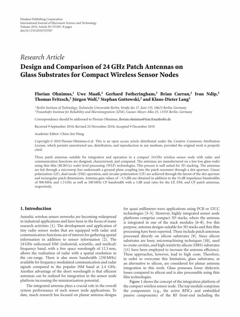
Figure 1 shows the concept of the integration platform ofthe compact wireless sensor node. The top module comprisesthe components (e.g., the active RFICs and embeddedpassive components) of the RF front-end including the
2 International Journal of Microwave Science and Technology
integrated planar antenna. The second module includesthe IF and baseband components. Both modules can beinterconnected using interstack bumps in a 3D build-up.
In this work, three 24 GHz patch antennas with differentmodes of operation which are suitable for integration inthe top RF module of the wireless sensor node are designedand characterized. The focus lies on the implementation andtest of these antennas at 24 GHz in combination with thinfilm technologies and fabrication on a glass substrate. Acomparison of the antennas based on full-wave simulationsand measurements is conducted.
This paper is divided into three sections. In Section 2, thepatch antenna concept and feeding techniques are explainedfollowed by the simulation results and analysis in Section 3.The results of an experimental characterization are presentedin Section 4.
2. Patch Antenna Concept andFeeding Technique
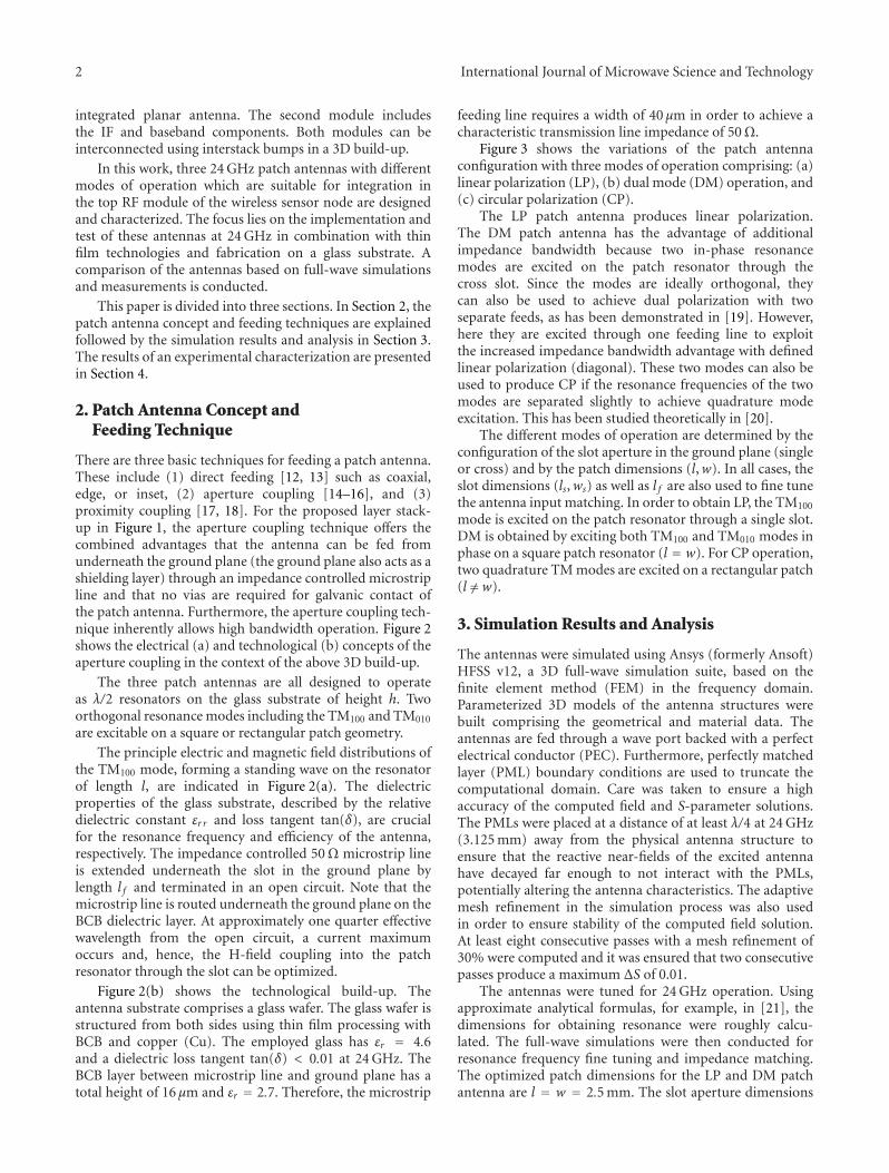
There are three basic techniques for feeding a patch antenna.These include (1) direct feeding [12, 13] such as coaxial,edge, or inset, (2) aperture coupling [14–16], and (3)proximity coupling [17, 18]. For the proposed layer stack-up in Figure 1, the aperture coupling technique offers thecombined advantages that the antenna can be fed fromunderneath the ground plane (the ground plane also acts as ashielding layer) through an impedance controlled microstripline and that no vias are required for galvanic contact ofthe patch antenna. Furthermore, the aperture coupling tech-nique inherently allows high bandwidth operation. Figure 2shows the electrical (a) and technological (b) concepts of theaperture coupling in the context of the above 3D build-up.
The three patch antennas are all designed to operateas λ/2 resonators on the glass substrate of height h. Twoorthogonal resonance modes including the TM100 and TM010
are excitable on a square or rectangular patch geometry.
The principle electric and magnetic field distributions ofthe TM100 mode, forming a standing wave on the resonatorof length l, are indicated in Figure 2(a). The dielectricproperties of the glass substrate, described by the relativedielectric constant εr r and loss tangent tan(δ), are crucialfor the resonance frequency and efficiency of the antenna,respectively. The impedance controlled 50Ω microstrip lineis extended underneath the slot in the ground plane bylength l f and terminated in an open circuit. Note that themicrostrip line is routed underneath the ground plane on theBCB dielectric layer. At approximately one quarter effectivewavelength from the open circuit, a current maximumoccurs and, hence, the H-field coupling into the patchresonator through the slot can be optimized.
Figure 2(b) shows the technological build-up. Theantenna substrate comprises a glass wafer. The glass wafer isstructured from both sides using thin film processing withBCB and copper (Cu). The employed glass has εr = 4.6and a dielectric loss tangent tan(δ) < 0.01 at 24 GHz. TheBCB layer between microstrip line and ground plane has atotal height of 16 μm and εr = 2.7. Therefore, the microstrip
feeding line requires a width of 40 μm in order to achieve acharacteristic transmission line impedance of 50Ω.
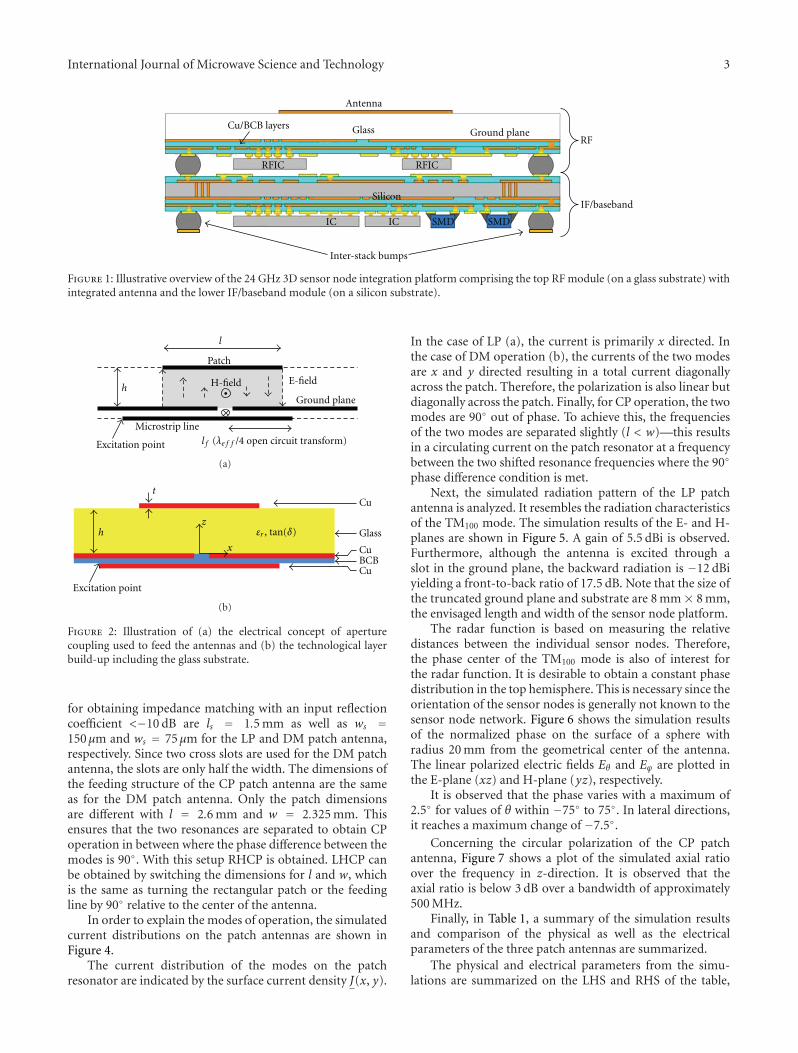
Figure 3 shows the variations of the patch antennaconfiguration with three modes of operation comprising: (a)linear polarization (LP), (b) dual mode (DM) operation, and(c) circular polarization (CP).
The LP patch antenna produces linear polarization.The DM patch antenna has the advantage of additionalimpedance bandwidth because two in-phase resonancemodes are excited on the patch resonator through thecross slot. Since the modes are ideally orthogonal, theycan also be used to achieve dual polarization with twoseparate feeds, as has been demonstrated in [19]. However,here they are excited through one feeding line to exploitthe increased impedance bandwidth advantage with definedlinear polarization (diagonal). These two modes can also beused to produce CP if the resonance frequencies of the twomodes are separated slightly to achieve quadrature modeexcitation. This has been studied theoretically in [20].
The different modes of operation are determined by theconfiguration of the slot aperture in the ground plane (singleor cross) and by the patch dimensions (l,w). In all cases, theslot dimensions (ls,ws) as well as l f are also used to fine tunethe antenna input matching. In order to obtain LP, the TM100
mode is excited on the patch resonator through a single slot.DM is obtained by exciting both TM100 and TM010 modes inphase on a square patch resonator (l = w). For CP operation,two quadrature TM modes are excited on a rectangular patch(l /=w).
3. Simulation Results and Analysis
The antennas were simulated using Ansys (formerly Ansoft)HFSS v12, a 3D full-wave simulation suite, based on thefinite element method (FEM) in the frequency domain.Parameterized 3D models of the antenna structures werebuilt comprising the geometrical and material data. Theantennas are fed through a wave port backed with a perfectelectrical conductor (PEC). Furthermore, perfectly matchedlayer (PML) boundary conditions are used to truncate thecomputational domain. Care was taken to ensure a highaccuracy of the computed field and S-parameter solutions.The PMLs were placed at a distance of at least λ/4 at 24 GHz(3.125 mm) away from the physical antenna structure toensure that the reactive near-fields of the excited antennahave decayed far enough to not interact with the PMLs,potentially altering the antenna characteristics. The adaptivemesh refinement in the simulation process was also usedin order to ensure stability of the computed field solution.At least eight consecutive passes with a mesh refinement of30% were computed and it was ensured that two consecutivepasses produce a maximum ΔS of 0.01.
The antennas were tuned for 24 GHz operation. Usingapproximate analytical formulas, for example, in [21], thedimensions for obtaining resonance were roughly calcu-lated. The full-wave simulations were then conducted forresonance frequency fine tuning and impedance matching.The optimized patch dimensions for the LP and DM patchantenna are l = w = 2.5 mm. The slot aperture dimensions
International Journal of Microwave Science and Technology 3
RFICRFIC
SMD SMDIC IC
Silicon
Glass
Antenna
Inter-stack bumps
Ground planeCu/BCB layers
RF
IF/baseband
Figure 1: Illustrative overview of the 24 GHz 3D sensor node integration platform comprising the top RF module (on a glass substrate) withintegrated antenna and the lower IF/baseband module (on a silicon substrate).
H-field
l f (λe f f /4 open circuit transform)
Ground plane
Microstrip line
Patch
E-field
l
h
Excitation point
(a)
h
Excitation point
εr , tan(δ)
BCB
Cu
Cu
Cu
Glass
t
x
z
(b)
Figure 2: Illustration of (a) the electrical concept of aperturecoupling used to feed the antennas and (b) the technological layerbuild-up including the glass substrate.
for obtaining impedance matching with an input reflectioncoefficient <−10 dB are ls = 1.5 mm as well as ws =150μm and ws = 75μm for the LP and DM patch antenna,respectively. Since two cross slots are used for the DM patchantenna, the slots are only half the width. The dimensions ofthe feeding structure of the CP patch antenna are the sameas for the DM patch antenna. Only the patch dimensionsare different with l = 2.6 mm and w = 2.325 mm. Thisensures that the two resonances are separated to obtain CPoperation in between where the phase difference between themodes is 90◦. With this setup RHCP is obtained. LHCP canbe obtained by switching the dimensions for l and w, whichis the same as turning the rectangular patch or the feedingline by 90◦ relative to the center of the antenna.
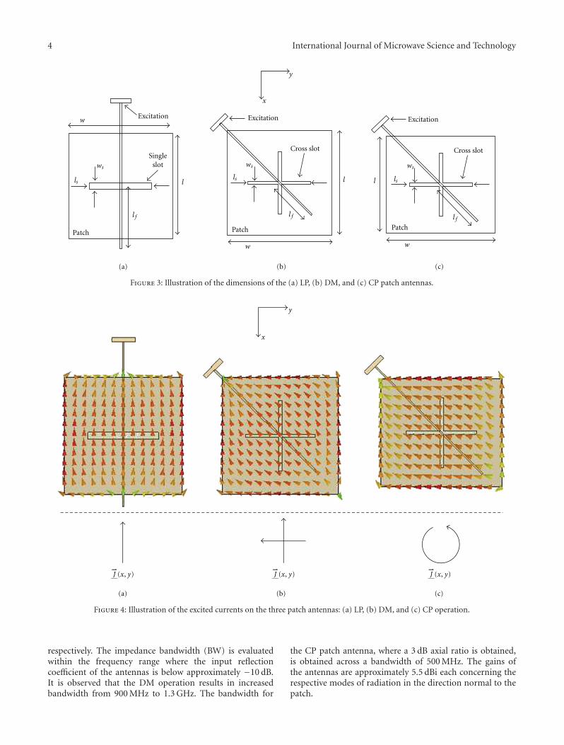
In order to explain the modes of operation, the simulatedcurrent distributions on the patch antennas are shown inFigure 4.
The current distribution of the modes on the patchresonator are indicated by the surface current density J(x, y).
In the case of LP (a), the current is primarily x directed. Inthe case of DM operation (b), the currents of the two modesare x and y directed resulting in a total current diagonallyacross the patch. Therefore, the polarization is also linear butdiagonally across the patch. Finally, for CP operation, the twomodes are 90◦ out of phase. To achieve this, the frequenciesof the two modes are separated slightly (l < w)—this resultsin a circulating current on the patch resonator at a frequencybetween the two shifted resonance frequencies where the 90◦
phase difference condition is met.Next, the simulated radiation pattern of the LP patch
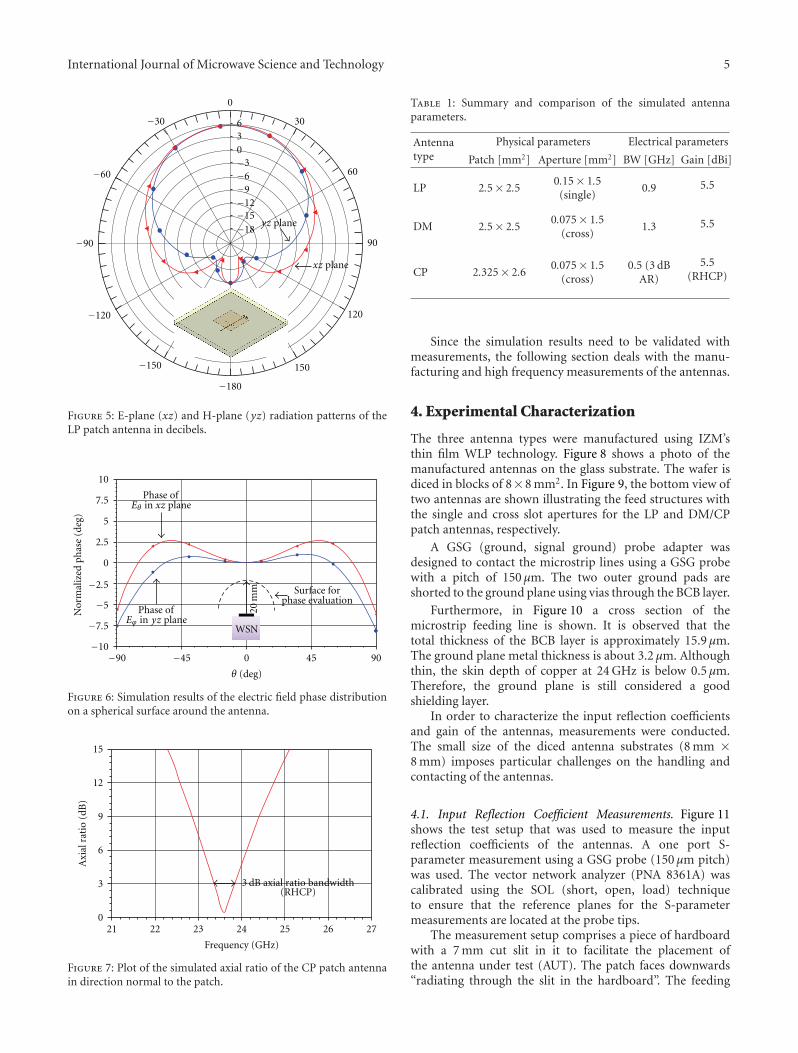
antenna is analyzed. It resembles the radiation characteristicsof the TM100 mode. The simulation results of the E- and H-planes are shown in Figure 5. A gain of 5.5 dBi is observed.Furthermore, although the antenna is excited through aslot in the ground plane, the backward radiation is −12 dBiyielding a front-to-back ratio of 17.5 dB. Note that the size ofthe truncated ground plane and substrate are 8 mm × 8 mm,the envisaged length and width of the sensor node platform.
The radar function is based on measuring the relativedistances between the individual sensor nodes. Therefore,the phase center of the TM100 mode is also of interest forthe radar function. It is desirable to obtain a constant phasedistribution in the top hemisphere. This is necessary since theorientation of the sensor nodes is generally not known to thesensor node network. Figure 6 shows the simulation resultsof the normalized phase on the surface of a sphere withradius 20 mm from the geometrical center of the antenna.The linear polarized electric fields Eθ and Eϕ are plotted inthe E-plane (xz) and H-plane (yz), respectively.
It is observed that the phase varies with a maximum of2.5◦ for values of θ within −75◦ to 75◦. In lateral directions,it reaches a maximum change of −7.5◦.
Concerning the circular polarization of the CP patchantenna, Figure 7 shows a plot of the simulated axial ratioover the frequency in z-direction. It is observed that theaxial ratio is below 3 dB over a bandwidth of approximately500 MHz.
Finally, in Table 1, a summary of the simulation resultsand comparison of the physical as well as the electricalparameters of the three patch antennas are summarized.
The physical and electrical parameters from the simu-lations are summarized on the LHS and RHS of the table,
4 International Journal of Microwave Science and Technology
Excitation Excitation Excitationw
w w
l l l
Singleslot
Cross slot Cross slot
Patch Patch Patch
lsls ls
ws ws ws
l f l f l f
y
x
(a) (b) (c)
Figure 3: Illustration of the dimensions of the (a) LP, (b) DM, and (c) CP patch antennas.
−→J (x, y)
−→J (x, y)
−→J (x, y)
x
y
(a) (b) (c)
Figure 4: Illustration of the excited currents on the three patch antennas: (a) LP, (b) DM, and (c) CP operation.
respectively. The impedance bandwidth (BW) is evaluatedwithin the frequency range where the input reflectioncoefficient of the antennas is below approximately −10 dB.It is observed that the DM operation results in increasedbandwidth from 900 MHz to 1.3 GHz. The bandwidth for
the CP patch antenna, where a 3 dB axial ratio is obtained,is obtained across a bandwidth of 500 MHz. The gains ofthe antennas are approximately 5.5 dBi each concerning therespective modes of radiation in the direction normal to thepatch.
International Journal of Microwave Science and Technology 5
yz plane
xz plane
0
30
60
120
150
−180
−150
−120
−90
−60
−30 630−3−6−9−12−15−18
90
Figure 5: E-plane (xz) and H-plane (yz) radiation patterns of theLP patch antenna in decibels.
Phase of
WSN
20m
m Surface forphase evaluation
θ (deg)
Nor
mal
ized
phas
e(d
eg)
−90 −45 0 45 90
10
7.5
5
2.5
0
−2.5
−5
−7.5
−10
Phase ofEϕ in yz plane
Eθ in xz plane
Figure 6: Simulation results of the electric field phase distributionon a spherical surface around the antenna.
3 dB axial ratio bandwidth
15
12
9
6
3
021 22 23 24 25 26 27
Axi
alra
tio
(dB
)
Frequency (GHz)
(RHCP)
Figure 7: Plot of the simulated axial ratio of the CP patch antennain direction normal to the patch.
Table 1: Summary and comparison of the simulated antennaparameters.
Antennatype
Physical parameters Electrical parameters
Patch [mm2] Aperture [mm2] BW [GHz] Gain [dBi]
LP 2.5× 2.50.15× 1.5
(single)0.9 5.5
DM 2.5× 2.50.075× 1.5
(cross)1.3 5.5
CP 2.325× 2.60.075× 1.5
(cross)0.5 (3 dB
AR)
5.5(RHCP)
Since the simulation results need to be validated withmeasurements, the following section deals with the manu-facturing and high frequency measurements of the antennas.
4. Experimental Characterization
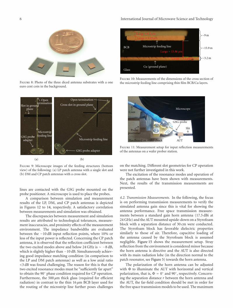
The three antenna types were manufactured using IZM’sthin film WLP technology. Figure 8 shows a photo of themanufactured antennas on the glass substrate. The wafer isdiced in blocks of 8×8 mm2. In Figure 9, the bottom view oftwo antennas are shown illustrating the feed structures withthe single and cross slot apertures for the LP and DM/CPpatch antennas, respectively.
A GSG (ground, signal ground) probe adapter wasdesigned to contact the microstrip lines using a GSG probewith a pitch of 150 μm. The two outer ground pads areshorted to the ground plane using vias through the BCB layer.
Furthermore, in Figure 10 a cross section of themicrostrip feeding line is shown. It is observed that thetotal thickness of the BCB layer is approximately 15.9 μm.The ground plane metal thickness is about 3.2 μm. Althoughthin, the skin depth of copper at 24 GHz is below 0.5 μm.Therefore, the ground plane is still considered a goodshielding layer.
In order to characterize the input reflection coefficientsand gain of the antennas, measurements were conducted.The small size of the diced antenna substrates (8 mm ×8 mm) imposes particular challenges on the handling andcontacting of the antennas.
4.1. Input Reflection Coefficient Measurements. Figure 11shows the test setup that was used to measure the inputreflection coefficients of the antennas. A one port S-parameter measurement using a GSG probe (150 μm pitch)was used. The vector network analyzer (PNA 8361A) wascalibrated using the SOL (short, open, load) techniqueto ensure that the reference planes for the S-parametermeasurements are located at the probe tips.
The measurement setup comprises a piece of hardboardwith a 7 mm cut slit in it to facilitate the placement ofthe antenna under test (AUT). The patch faces downwards“radiating through the slit in the hardboard”. The feeding
6 International Journal of Microwave Science and Technology
Figure 8: Photo of the three diced antenna substrates with a oneeuro cent coin in the background.
Cross slot in ground plane
Microstrip feeding line
GSG probe adapter
Open termination
Slot in groundplane
Microstripfeeding lineGSG probe
adapter
Opentermination
(a) (b)
Figure 9: Microscope images of the feeding structures (bottomview) of the following: (a) LP patch antenna with a single slot and(b) DM and CP patch antennas with a cross slot.
lines are contacted with the GSG probe mounted on theprobe positioner. A microscope is used to place the probes.
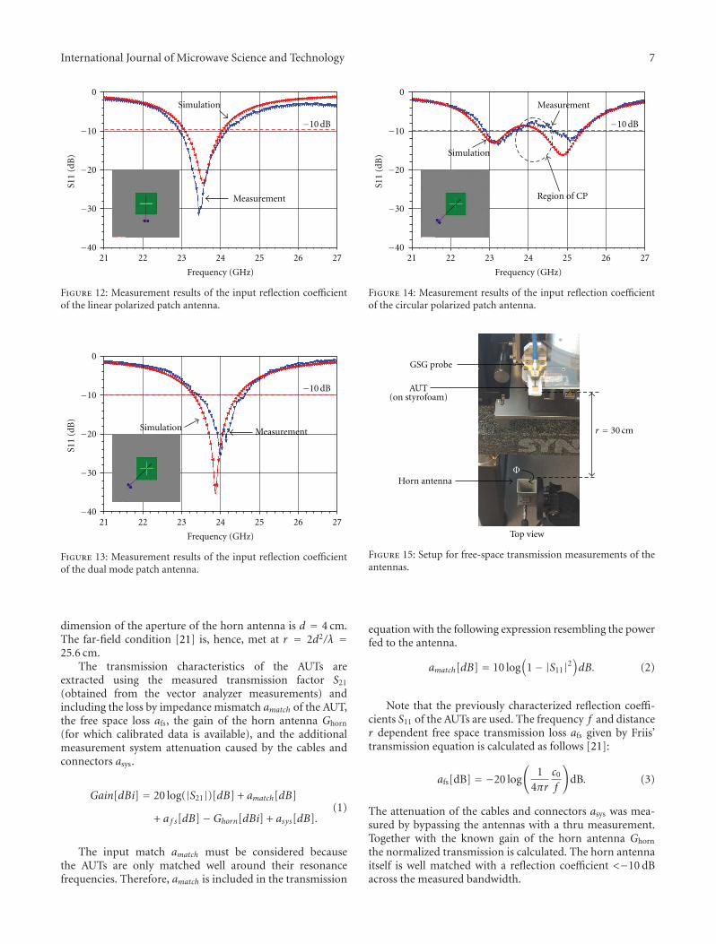
A comparison between simulation and measurementresults of the LP, DM, and CP patch antennas is depictedin Figures 12 to 14, respectively. A satisfactory correlationbetween measurements and simulation was obtained.
The discrepancies between measurement and simulationresults are attributed to technological tolerances, measure-ment inaccuracies, and proximity effects of the measurementenvironment. The impedance bandwidths are evaluatedbetween the −10 dB input reflection points, where 10% orless of the input power is reflected. Concerning the CP patchantenna, it is observed that the reflection coefficient betweenthe two excited modes above and below 24 GHz is ∼ −8 dB,which is slightly higher than −10 dB. Simultaneously achiev-ing good impedance matching condition (in comparison tothe LP and DM patch antennas) as well as a low axial ratio<3 dB was found challenging. The reason for this is that thetwo excited resonance modes must be “sufficiently far apart”to obtain the 90◦ phase condition required for CP operation.Furthermore, the 500 μm thick glass (required for efficientradiation) in contrast to the thin 16 μm BCB layer used forthe routing of the microstrip line further poses challenges
Glass
BCB
Cu (ground plane)
Microstrip feeding line
∼9 m
∼15.9 m
∼3.2 m
Lange = 4.2 μm
Lange = 4.83 μm
Lange = 3.2 μm
Lange = 15.86 μm
Figure 10: Measurements of the dimensions of the cross section ofthe microstrip feeding line comprising thin film BCB/Cu layers.
GSG-probe
Microscope
Hardboard on wafer-chuck
Coax
AUT
SlitProbe
positioner
Figure 11: Measurement setup for input reflection measurementsof the antennas on a wafer prober station.
on the matching. Different slot geometries for CP operationwere not further investigated in this work.
The excitation of the resonance modes and operation ofthe patch antennas have been shown with measurements.Next, the results of the transmission measurements arepresented.
4.2. Transmission Measurements. In the following, the focusis on performing transmission measurements to verify thesimulated antenna gain since this is vital for showing theantenna performance. Free space transmission measure-ments between a standard gain horn antenna (17.5 dBi at24 GHz) and the AUT mounted upside-down on a Styrofoamblock with a separation distance of 30 cm were conducted.The Styrofoam block has favorable dielectric propertiessimilarly to those of air. Therefore, capacitive loading ofthe antenna caused by the Styrofoam block is assumednegligible. Figure 15 shows the measurement setup. Strayreflection from the environment is considered minor becausethe horn antenna is directive and the AUT is also directedwith its main radiation lobe (in the direction normal to thepatch resonator, see Figure 5) towards the horn antenna.
The polarization of the horn antenna can be adjustedwith Φ to illuminate the AUT with horizontal and verticalpolarization, that is, Φ = 0◦ and 90◦, respectively. Concern-ing the separation distance r between the horn antenna andthe AUT, the far-field condition should be met in order forthe free space transmission models to be used. The maximum
International Journal of Microwave Science and Technology 7
Simulation
Measurement
−10 dB
0
−10
−20
−30
−4021 22 23 24 25 26 27
S11
(dB
)
Frequency (GHz)
Figure 12: Measurement results of the input reflection coefficientof the linear polarized patch antenna.
Simulation Measurement
−10 dB
0
−10
−20
−30
−4021 22 23 24 25 26 27
S11
(dB
)
Frequency (GHz)
Figure 13: Measurement results of the input reflection coefficientof the dual mode patch antenna.
dimension of the aperture of the horn antenna is d = 4 cm.The far-field condition [21] is, hence, met at r = 2d2/λ =25.6 cm.
The transmission characteristics of the AUTs areextracted using the measured transmission factor S21
(obtained from the vector analyzer measurements) andincluding the loss by impedance mismatch amatch of the AUT,the free space loss afs, the gain of the horn antenna Ghorn
(for which calibrated data is available), and the additionalmeasurement system attenuation caused by the cables andconnectors asys.
Gain[dBi] = 20 log(|S21|)[dB] + amatch[dB]
+ a f s[dB]−Ghorn[dBi] + asys[dB].(1)
The input match amatch must be considered becausethe AUTs are only matched well around their resonancefrequencies. Therefore, amatch is included in the transmission
Simulation
Measurement
−10 dB
0
−10
−20
−30
−4021 22 23 24 25 26 27
S11
(dB
)
Frequency (GHz)
Region of CP
Figure 14: Measurement results of the input reflection coefficientof the circular polarized patch antenna.
GSG probe
r = 30 cm
AUT(on styrofoam)
Horn antenna
Top view
Φ
Figure 15: Setup for free-space transmission measurements of theantennas.
equation with the following expression resembling the powerfed to the antenna.
amatch[dB] = 10 log(
1− |S11|2)dB. (2)
Note that the previously characterized reflection coeffi-cients S11 of the AUTs are used. The frequency f and distancer dependent free space transmission loss afs given by Friis’transmission equation is calculated as follows [21]:
afs[dB] = −20 log
(1
4πrc0
f
)dB. (3)
The attenuation of the cables and connectors asys was mea-sured by bypassing the antennas with a thru measurement.Together with the known gain of the horn antenna Ghorn
the normalized transmission is calculated. The horn antennaitself is well matched with a reflection coefficient <−10 dBacross the measured bandwidth.
8 International Journal of Microwave Science and Technology
Measured gainover 5 dBi
Normalized transmission betweentwo isotropic antennas
10
5
0
−5
−10
−1521 22 23 24 25 26 27
Tran
smis
sion
(dB
)
Frequency (GHz)
Figure 16: Measurement results of the transmission between thelinear polarized patch antenna and the horn antenna.
Measured gainover 5 dBi
Normalized transmission betweentwo isotropic antennas
10
5
0
−5
−10
−1521 22 23 24 25 26 27
Tran
smis
sion
(dB
)
Frequency (GHz)
Note: polarization of horn antenna is slanted (Φ = 45◦)
Figure 17: Measurement results of the transmission between thedual mode patch antenna and the horn antenna.
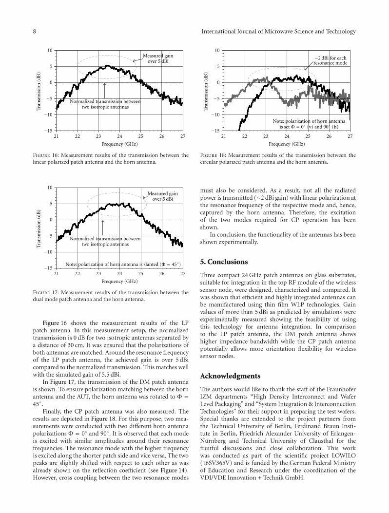
Figure 16 shows the measurement results of the LPpatch antenna. In this measurement setup, the normalizedtransmission is 0 dB for two isotropic antennas separated bya distance of 30 cm. It was ensured that the polarizations ofboth antennas are matched. Around the resonance frequencyof the LP patch antenna, the achieved gain is over 5 dBicompared to the normalized transmission. This matches wellwith the simulated gain of 5.5 dBi.
In Figure 17, the transmission of the DM patch antennais shown. To ensure polarization matching between the hornantenna and the AUT, the horn antenna was rotated to Φ =45◦.
Finally, the CP patch antenna was also measured. Theresults are depicted in Figure 18. For this purpose, two mea-surements were conducted with two different horn antennapolarizations Φ = 0◦ and 90◦. It is observed that each modeis excited with similar amplitudes around their resonancefrequencies. The resonance mode with the higher frequencyis excited along the shorter patch side and vice versa. The twopeaks are slightly shifted with respect to each other as wasalready shown on the reflection coefficient (see Figure 14).However, cross coupling between the two resonance modes
10
5
0
−5
−10
−1521 22 23 24 25 26 27
Tran
smis
sion
(dB
)
Frequency (GHz)
∼2 dBi for eachresonance mode
Note: polarization of horn antennais set Φ = 0◦ (v) and 90◦ (h)
Figure 18: Measurement results of the transmission between thecircular polarized patch antenna and the horn antenna.
must also be considered. As a result, not all the radiatedpower is transmitted (∼2 dBi gain) with linear polarization atthe resonance frequency of the respective mode and, hence,captured by the horn antenna. Therefore, the excitationof the two modes required for CP operation has beenshown.
In conclusion, the functionality of the antennas has beenshown experimentally.
5. Conclusions
Three compact 24 GHz patch antennas on glass substrates,suitable for integration in the top RF module of the wirelesssensor node, were designed, characterized and compared. Itwas shown that efficient and highly integrated antennas canbe manufactured using thin film WLP technologies. Gainvalues of more than 5 dBi as predicted by simulations wereexperimentally measured showing the feasibility of usingthis technology for antenna integration. In comparisonto the LP patch antenna, the DM patch antenna showshigher impedance bandwidth while the CP patch antennapotentially allows more orientation flexibility for wirelesssensor nodes.
Acknowledgments
The authors would like to thank the staff of the FraunhoferIZM departments “High Density Interconnect and WaferLevel Packaging” and “System Integration & InterconnectionTechnologies” for their support in preparing the test wafers.Special thanks are extended to the project partners fromthe Technical University of Berlin, Ferdinand Braun Insti-tute in Berlin, Friedrich Alexander University of Erlangen-Nurnberg and Technical University of Clausthal for thefruitful discussions and close collaboration. This workwas conducted as part of the scientific project LOWILO(16SV365V) and is funded by the German Federal Ministryof Education and Research under the coordination of theVDI/VDE Innovation + Technik GmbH.
International Journal of Microwave Science and Technology 9
References
[1] M. Niedermayer, S. Guttowski, R. Thomasius, D. Polityko,K. Schrank, and H. Reichl, “Miniaturization platform forwireless sensor nodes based on 3D-packaging technologies,” inProceedings of the 5th International Conference on InformationProcessing in Sensor Networks (IPSN ’06), pp. 391–398, April2006.
[2] R. Ebelt, H. Millner, and M. Vossiek, “Wireless network-to-network localization for measuring the spatial positionand orientation of vehicles,” in Proceedings of the IEEEInternational Conference on Wireless Information Technologyand Systems (ICWITS ’10), Honolulu, Hawaii, USA, August2010.
[3] F. Ohnimus, A. Podlasly, J. Bauer et al., “Electrical designand characterization of elevated antennas at PCB-level,” inProceedings of the 59th Electronic Components and TechnologyConference (ECTC ’09), pp. 1618–1623, May 2009.
[4] P. R. Grajek, B. Schoenlinner, and G. M. Rebeiz, “A 24-GHz high-gain Yagi-Uda antenna array,” IEEE Transactions onAntennas and Propagation, vol. 52, no. 5, pp. 1257–1261, 2004.
[5] T. Seki, N. Honma, K. Nishikawa, and K. Tsunekawa, “A60-GHz multilayer parasitic microstrip array antenna onLTCC substrate for system-on-package,” IEEE Microwave andWireless Components Letters, vol. 15, no. 5, pp. 339–341, 2005.
[6] H. Reichl and M. J. Wolf, “System integration technologiesfor ultra small systems,” in Proceedings of the 11th IEEE Inter-national Symposium and Exhibition on Advanced PackagingMaterials Processes, Properties and Interfaces, p. 11, Atlanta, Ga,USA, 2006.
[7] P. K. Talukder, M. Neuner, C. Meliani, F. J. Schmuckle, and W.Heinrich, “A 24 GHz active antenna in flip-chip technologywith integrated frontend,” in Proceedings of the IEEE MTT-S International Microwave Symposium Digest, pp. 1776–1779,June 2006.
[8] M. M. Hella, S. Devarajan, J. Q. Lu, K. Rose, and R. J.Gutmann, “Die-on-wafer and wafer-level 3D integration formillimeter-wave smart antenna transceivers,” in Proceedingsof the IEEE Annual Conference on Wireless and MicrowaveTechnology (WAMICON ’05), pp. 125–128, April 2005.
[9] R. Carrillo-Ramirez and R. W. Jackson, “A highly integratedmillimeter-wave active antenna array using BCB and siliconsubstrate,” IEEE Transactions on Microwave Theory and Tech-niques, vol. 52, no. 6, pp. 1648–1653, 2004.
[10] J. G. Yook and L. P. B. Katehi, “Micromachined microstrippatch antenna with controlled mutual coupling and surfacewaves,” IEEE Transactions on Antennas and Propagation, vol.49, no. 9, pp. 1282–1289, 2001.
[11] P. M. Mendes, S. Sinaga, A. Polyakov, M. Bartek, J. N.Burghartz, and J. H. Correia, “Wafer-level integration of on-chip antennas and RF passives using high-resistivity polysili-con substrate technology,” in Proceedings of the 54th ElectronicComponents and Technology Conference, pp. 1879–1884, June2004.
[12] A. Latif, A. Oulad-Said, and A. A. Ouahman, “Passage from aninset-fed rectangular patch antenna to an end-fed and probe-fed rectangular patch antenna, modelling and analyses,” inProceedings of the IEEE International Conference on IndustrialTechnology (ICIT ’04), pp. 932–937, December 2004.
[13] B. M. Alarjani and J. S. Dahele, “Feed reactance of rectangularmicrostrip patch antenna with probe feed,” Electronics Letters,vol. 36, no. 5, pp. 388–390, 2000.
[14] Y. Murakami, S. Sekine, and H. Shoki, “Analysis of cross-slot-coupled circular microstrip antenna,” Electronics Letters, vol.38, no. 25, pp. 1619–1621, 2002.
[15] B. Ai-Jibouri, T. Viasits, E. Korolkiewicz, S. Scott, and A.Sambell, “Transmission-line modelling of the cross-aperture-coupled circular polarised microstrip antenna,” IEE Proceed-ings: Microwaves, Antennas and Propagation, vol. 147, no. 2,pp. 82–86, 2000.
[16] W. Yi, W. Lei, and S. Yunqing, “Design of L-circularlypolarized microstrip antenna array at Ka band,” in Proceedingsof the International Conference Microwave and Millimeter WaveTechnology (ICMMT ’10), Chengdu, China, May 2010.
[17] W. S. T. Rowe and R. B. Waterhouse, “Investigation of prox-imity coupled patch antennas suitable for MMIC integration,”in Proceedings of the International Symposium on Antennas andPropagation, pp. 1591–1594, June 2004.
[18] S. Vajha and P. Shastry, “A novel proximity coupled patchantenna for active circuit integration,” in Proceedings ofthe IEEE Antennas and Propagation Society InternationalSymposium-Adaptive Arrays in Communications-, pp. 772–775, July 2001.
[19] D. G. Kim, C. B. Smith, C.-H. Ahn, and K. Chang, “Adual-polarization aperture coupled stacked microstrip patchantenna for wideband application,” in Proceedings of the IEEEInternational Symposium on Antennas and Propagation andCNC-USNC/URSI Radio Science Meeting—Leading the Wave(AP-S/URSI ’10), Toronto, Canada, July 2010.
[20] B. Al-Jibouri, H. Evans, E. Korolkiewicz, E. G. Lim, A.Sambell, and T. Viasits, “Cavity model of circularly polarisedcross-aperture-coupled microstrip antenna,” IEE Proceedings:Microwaves, Antennas and Propagation, vol. 148, no. 3, pp.147–152, 2001.
[21] C. A. Balanis, Antenna Theory—Analysis and Design, 2ndedition, 1997.

International Journal of
AerospaceEngineeringHindawi Publishing Corporationhttp://www.hindawi.com Volume 2010
RoboticsJournal of
Hindawi Publishing Corporationhttp://www.hindawi.com Volume 2014
Hindawi Publishing Corporationhttp://www.hindawi.com Volume 2014
Active and Passive Electronic Components
Control Scienceand Engineering
Journal of
Hindawi Publishing Corporationhttp://www.hindawi.com Volume 2014
International Journal of
RotatingMachinery
Hindawi Publishing Corporationhttp://www.hindawi.com Volume 2014
Hindawi Publishing Corporation http://www.hindawi.com
Journal ofEngineeringVolume 2014
Submit your manuscripts athttp://www.hindawi.com
VLSI Design
Hindawi Publishing Corporationhttp://www.hindawi.com Volume 2014
Hindawi Publishing Corporationhttp://www.hindawi.com Volume 2014
Shock and Vibration
Hindawi Publishing Corporationhttp://www.hindawi.com Volume 2014
Civil EngineeringAdvances in
Acoustics and VibrationAdvances in
Hindawi Publishing Corporationhttp://www.hindawi.com Volume 2014
Hindawi Publishing Corporationhttp://www.hindawi.com Volume 2014
Electrical and Computer Engineering
Journal of
Advances inOptoElectronics
Hindawi Publishing Corporation http://www.hindawi.com
Volume 2014
The Scientific World JournalHindawi Publishing Corporation http://www.hindawi.com Volume 2014
SensorsJournal of
Hindawi Publishing Corporationhttp://www.hindawi.com Volume 2014
Modelling & Simulation in EngineeringHindawi Publishing Corporation http://www.hindawi.com Volume 2014
Hindawi Publishing Corporationhttp://www.hindawi.com Volume 2014
Chemical EngineeringInternational Journal of Antennas and
Propagation
International Journal of
Hindawi Publishing Corporationhttp://www.hindawi.com Volume 2014
Hindawi Publishing Corporationhttp://www.hindawi.com Volume 2014
Navigation and Observation
International Journal of
Hindawi Publishing Corporationhttp://www.hindawi.com Volume 2014
DistributedSensor Networks
International Journal of