Design of OTA Based Chebyshev 5th Order Low Pass Filter in ... · an op-amp without output...
4
Design of OTA Based Chebyshev 5 th Order Low Pass Filter in 0.18μm CMOS Technology NEERAJ SHRIVASTAVA #1 , GAURAV BHARGAVA #2 , D.S AJNAR #3 , PRAMOD KUMAR JAIN #4 , #1, 2, 3, 4 Micro Electronics and VLSI design ** Electronics & Instrumentation Engineering department, SGSITS, Indore, M.P., India #1 Email Id:[email protected], #2 Email Id:[email protected], #3 Email Id:[email protected], #4 Email Id:[email protected] ***Correspondence/Courier Address: CM-II/59,MIG Duplex,Sukhliya,Dist.-Indore (M.P.), Pin code: 452010, India 1.Abstract:The design of OTA based low pass filter for video applications in Broadband Communication is described in this paper. A low-pass, fifth-order Chebyshev filter based on the Folded Cascode Operational Transconductance Amplifier in0.18 um CMOS process is designed.Folded Cascode OTA is chosen as it allows shorting of input and output terminals with negligible swing limitations. The designed OTA has a DC gain of 72.75dB and provides a Unity Gain Bandwidth of 17MHz.The filterdesigned using this OTA has a passband frequency response of 9.2MHz and gain of 0dB. Design and simulation ofthe circuit is done in Cadence spectre environment using UMC0.18 μm CMOS technology. Keywords: Analog IC design, Folded Cascode OTA, Chebyshev low pass filter. 2.Introduction A filter is defined as an electric network, which passes or allows unattenuated transmission of electric signal within certain frequency range and stops or disallows transmission of electric signal outside this range.The term Chebyshev refers to a type of filter response, not a type of filter. Chebyshev filters have the property that they minimise the error between the idealised filter characteristic and the actual over the range of the filter, but with ripples in the passband. As the ripple increases (bad), the roll-off becomes sharper (good).The response of Chebyshev filters is based on the minimization of the maximum error in the entire passband, resulting in passband ripples with equal amplitude. The greater the ripple amplitude allowed, the steeper the transition roll-off. Chebyshev filters are also known as “equiripple” or “minimax” filters because of their characteristics. The operational transconductance amplifier (OTA)is basically an op-amp without output buffer.The bias voltage in an OTA controls the bias current flowing through the current mirror circuit, which in turns affects the “gm”. All the standard filter parameters of interest are directly proportional to “gm” of the OTA.The primary advantage of folded structure lies in the choice of voltage levels because it does not “stack” the cascode transistor on the top of the input device. The folded cascade does not require perfect balance of currents in differential amplifier because excess DC current can flow into or out of current mirror. 3. Circuit Implementation 3.1 Folded Cascode CMOS OTA Design: Design of OTA is very importantto get accurate filter results.The OTA is characterized by various parameters like Gain at dc (A V ),Unity gain bandwidth(UGB),Input common mode range (Vin (min) and Vin (max)),Load capacitance (C L ).All the sources are connected to their bulk reducing the body bias effect to zero. The input voltage is applied at one end and the other end is grounded.Because the drains of M1 and M2 are connected to drains of M4 and M5, a positive input common mode voltage that can be achieved by using current source loads is achieved. For the maximum gain to achieve, all the transistors are made to work in saturation region. Figure 3.1 Schematic of CMOS OTA Table.3.1 CMOS Transistor sizing for OTA Design S. NO. DEVICE W/L(um) 1 M1,M2 50/2.0 2 M3 281/2.0 3 M4,M5,M6,M7 303/2.0 4 M8,M9,M10,M11 75/2.0 5 M12 351/2.0 Proc. of the Intl. Conf. on Advances in Computer Science and Electronics Engineering Editor In Chief Sahil Seth. Copyright © 2012 Universal Association of Computer and Electronics Engineers. All rights reserved. ISBN: 978-981-07-1403-1 doi:10.3850/978-981-07-1403-1 586 249
Transcript of Design of OTA Based Chebyshev 5th Order Low Pass Filter in ... · an op-amp without output...
Design of OTA Based Chebyshev 5th Order Low Pass Filter in 0.18μm CMOS Technology
NEERAJ SHRIVASTAVA#1 , GAURAV BHARGAVA#2 , D.S AJNAR#3 , PRAMOD KUMAR JAIN #4,#1, 2, 3, 4Micro Electronics and VLSI design
** Electronics & Instrumentation Engineering department, SGSITS, Indore, M.P., India#1Email Id:[email protected], #2Email Id:[email protected],
#3Email Id:[email protected],#4Email Id:[email protected]***Correspondence/Courier Address: CM-II/59,MIG Duplex,Sukhliya,Dist.-Indore (M.P.), Pin code: 452010, India
1.Abstract:The design of OTA based low pass filter for video applications in Broadband Communication is described in this paper. A low-pass, fifth-order Chebyshev filter based on the Folded Cascode Operational Transconductance Amplifier in0.18 um CMOS process is designed.Folded Cascode OTA is chosen as it allows shorting of input and output terminals with negligible swing limitations. The designed OTA has a DC gain of 72.75dB and provides a Unity Gain Bandwidth of 17MHz.The filterdesigned using this OTA has a passband frequency response of 9.2MHz and gain of 0dB. Design and simulation ofthe circuit is done in Cadence spectre environment using UMC0.18 μm CMOS technology.
Keywords: Analog IC design, Folded Cascode OTA, Chebyshev low pass filter.
2.Introduction
A filter is defined as an electric network, which passes or allows unattenuated transmission of electric signal within certain frequency range and stops or disallows transmission of electric signal outside this range.The term Chebyshev refers to a type of filter response, not a type of filter. Chebyshev filters have the property that they minimise the error between the idealised filter characteristic and the actual over the range of the filter, but with ripples in the passband. As the ripple increases (bad), the roll-off becomes sharper (good).The response of Chebyshev filters is based on the minimization of the maximum error in the entire passband, resulting in passband ripples with equal amplitude. The greater the ripple amplitude allowed, the steeper the transition roll-off. Chebyshev filters are also known as “equiripple” or“minimax” filters because of their characteristics.
The operational transconductance amplifier (OTA)is basically an op-amp without output buffer.The bias voltage in an OTA controls the bias current flowing through the current mirror circuit, which in turns affects the “gm”. All the standard filter parameters of interest are directly proportional to “gm” of the OTA.The primary advantage of folded structure lies in the choice of voltage levels because it does not “stack” the cascode transistor on the top of the input device. The folded cascade does not require perfect balance of currents in differential amplifier because excess DC current can flow into or out of current mirror.
3. Circuit Implementation
3.1 Folded Cascode CMOS OTA Design:
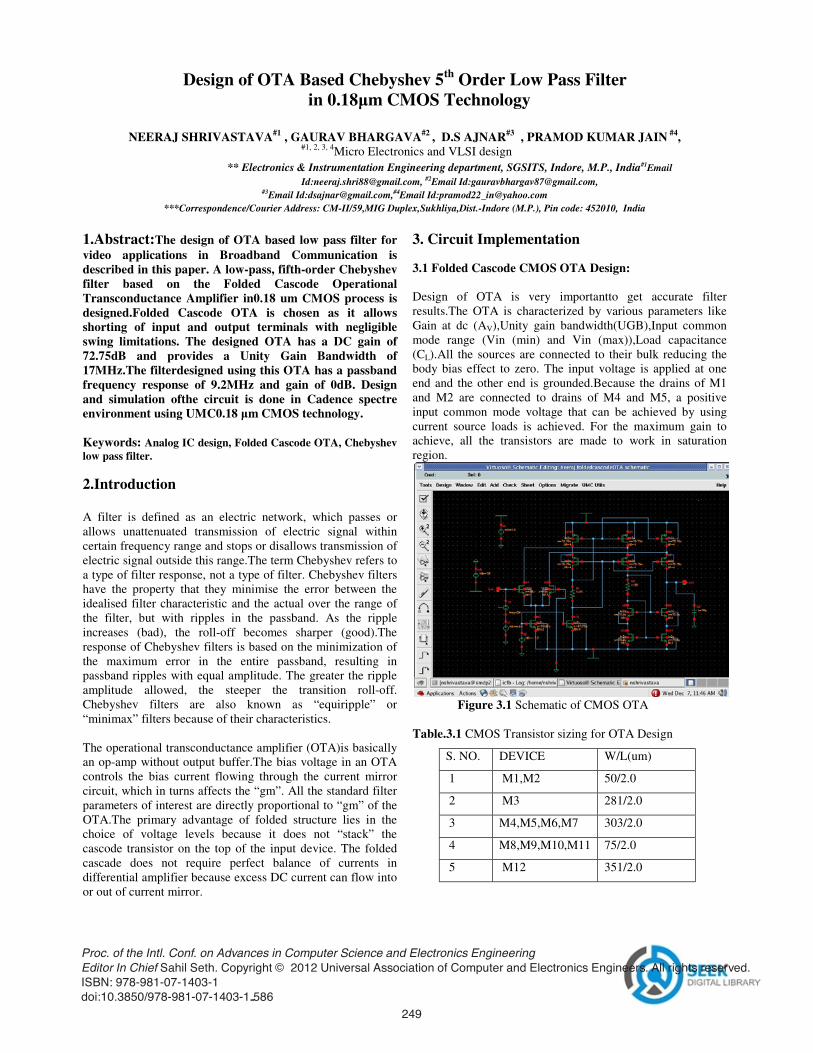
Design of OTA is very importantto get accurate filter results.The OTA is characterized by various parameters like Gain at dc (AV),Unity gain bandwidth(UGB),Input common mode range (Vin (min) and Vin (max)),Load capacitance (CL).All the sources are connected to their bulk reducing the body bias effect to zero. The input voltage is applied at one end and the other end is grounded.Because the drains of M1 and M2 are connected to drains of M4 and M5, a positive input common mode voltage that can be achieved by using current source loads is achieved. For the maximum gain to achieve, all the transistors are made to work in saturation region.
Figure 3.1 Schematic of CMOS OTA
Table.3.1 CMOS Transistor sizing for OTA Design
S. NO. DEVICE W/L(um)
1 M1,M2 50/2.0
2 M3 281/2.0
3 M4,M5,M6,M7 303/2.0
4 M8,M9,M10,M11 75/2.0
5 M12 351/2.0
Proc. of the Intl. Conf. on Advances in Computer Science and Electronics EngineeringEditor In Chief Sahil Seth. Copyright © 2012 Universal Association of Computer and Electronics Engineers. All rights reserved.ISBN: 978-981-07-1403-1doi:10.3850/978-981-07-1403-1 586
249
Proc. of the Intl. Conf. on Advances in Computer Science and Electronics Engineering
4. Result of OTA:
4.1Gain and Phase of OTA:
Table.4.1 SUMMARY OF EXPERIMENTAL RESULTS
S.NO. Experimental Value
1 VDD 1.8V
2 Gain 72.75dB
3 3dB frequency 1kHz
4 Input AC supply 2V,5MHz
5 Unity Gain Frequency 16.699 MHz
6 Load capacitance 15pF
7 Input Offset Voltage 4.2mV
8 Input Bias Voltage -1.3V
9 Gain Margin 36.85dB
10 Phase Margin 73.640
5.Architecture of Chebyshev Low Pass Filter
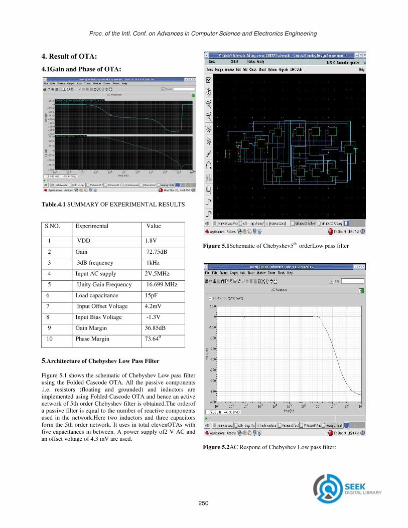
Figure 5.1 shows the schematic of Chebyshev Low pass filter using the Folded Cascode OTA. All the passive components .i.e. resistors (floating and grounded) and inductors are implemented using Folded Cascode OTA and hence an active network of 5th order Chebyshev filter is obtained.The orderof a passive filter is equal to the number of reactive components used in the network.Here two inductors and three capacitors form the 5th order network. It uses in total elevenOTAs with five capacitances in between. A power supply of2 V AC and an offset voltage of 4.3 mV are used.
Figure 5.1Schematic of Chebyshev5th orderLow pass filter
Figure 5.2AC Respone of Chebyshev Low pass filter:
250
Proc. of the Intl. Conf. on Advances in Computer Science and Electronics Engineering
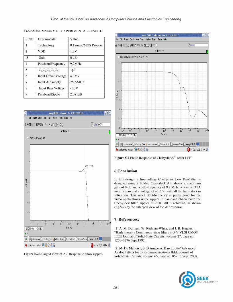
Table.5.2SUMMARY OF EXPERIMENTAL RESULTS
S.NO. Experimental Value
1 Technology 0.18um CMOS Process
2 VDD 1.8V
3 Gain 0 dB
4 PassbandFrequency 9.2MHz
5 C1,C2,C3,C4,C5 1pF
6 Input Offset Voltage 4.3Mv
7 Input AC supply 2V,5MHz
8 Input Bias Voltage -1.3V
9 PassbandRipple 2.081dB
Figure 5.2Enlarged view of AC Respone to show ripples
Figure 5.2 Phase Response of Chebyshev5th order LPF
6.Conclusion
In this design, a low-voltage Chebyshev Low PassFilter is designed using a Folded CascodeOTA.It shows a maximum gain of 0 dB and a 3dB-frequency of 9.2 MHz, when the OTA used is biased at a voltage of –1.3 V, with all the transistors in saturation. This much 3dB-frequency is pretty good for the video applications.Asthe ripples in passband characterize the Chebyshev filter, ripples of 2.081 dB is achieved, as shown (fig.5.2) by the enlarged view of the AC response.
7. References:
[1] A. M. Durham, W. Redman-White, and J. B. Hughes, “High linearity Continuous -time filters in 5-V VLSI CMOS IEEE Journal of Solid-State Circuits, volume 27, page no. 1270–1276 Sept.1992.
[2] M. De Matteis1, S. D Amico A. Baschirotto“Advanced Analog Filters for Telecomm-unications IEEE Journal of Solid-State Circuits, volume 65, page no. 06–12, Sept. 2008.
251

Proc. of the Intl. Conf. on Advances in Computer Science and Electronics Engineering
[3] H. Huang and E. K. F. Lee,“Design of lowCMOS continuous time filter with on chip auIEEE Journal of Solid-State Circuits, volume1168–1177 Aug. 2005.
[4] A. A. Hussain, O. Elwan Hassan, and Ism“A CMOS Highly Linear Channel-Select FiltMultistandard Integrated Wireless Receivers”journal of Solid-State Circuits, vol. 37, no. 1,
[5] Darwin Cheung, KlaasBulty and Aaron BMHz 60-dB Dynamic-Range 4th-Order ButteFilter”, IEEE press.
[6] DeyasiniMajumdar and Brent J. MaundGm-C filters and OTAs for HDSL2”, Mayima 2003.
Authors Profile:
NEERAJ SHRIVASTAVA
He has received the B.E. degreeTelecommunication Engineering from ChhVivekanand Technical University, Bhilai in 20pursuing M.Tech degree in Microelectronics and S.G.S.I.T.S. Indore, India.
GAURAV BHARGAVA
He has received the B.E. degreeCommunication Engineering from Rajiv GUniversity Bhopal, in 2009.He is currently pursuiMicroelectronics and VLSI Design from S.G.S.I.T
w – voltage utomatic tuning e 36 page no.
mail Mohammed, ter for 3G ”, IEEE, January 2002.
Buchwaldy, “10-erworth Lowpass
dy, “Low voltage IEEE, Montreal,
e in Electronics and hattisgarh Swami 010 .Heis currently
VLSI Design from
e in Electronics and Gandhi Technical ing M.Techdegreein T.S. Indore, Indore.
D.S AJNAR
He has received thand Communication Engineeringfrom D1993 andM.E. Degree in Digital TeEngineering from RajivGandhi Technica2000. He has been in teaching and ResHe is now working as Sr.Lecturer in Instrumentation Engineering, S.G.S.I.T.of research is in designing of analog filte
PRAMOD KUMAR JAIN
He has received theand Communication Engineeringfrom D1987 and M.E. Degree in Digital TEngineering from Rajiv Gandhi Technicin1993. He has been in teaching and1988.He is now working as Reader in Instrumentation Engineering, S.G.S.I.Tresearch is in Analog and digital system
he B.E. degree inElectronics D.A.V.V.University, India in echniques &Instrumentation al University Bhopal, India in earch Profession since 1995. Departmentof Electronics & .S.,Indore, India. His interest er and Current conveyer.
e B.E. degree in Electronics D.A.V.V. University, India in echniques &Instrumentation cal University, Bhopal, India
d Research Profession since Departmentof Electronics &
T.S.,Indore. His interest of design.
252