
An Extended-Range Ethernet and Clock Distribution Circuit for Distributed Sensor Networks
Abstract—A non-overlapping clock (NOC) generator circuit
is designed for the successful operation of high voltage
generator (HVG) implementation in low-power applications
like radio frequency identification (RFID) tag EEPROM. The
NOC generator has been implemented in 0.18 μm CMOS
process. The designed NOC can generate two stable anti-phase
clock signals as output, which is used in charge pump (CP)
circuit with low power dissipation. The NOC generator
required lower power dissipation with 359.87 nW under power
supply voltage (VDD) 1.8 V. Moreover, this designed NOC
generator produced faster clock signals with 0.972 μS as the
settling time.
Index Terms—NOC, HVG, RFID, CP, EEPROM.
I. INTRODUCTION
RFID is an identification system, which is used to transfer
and receive data from the tag/transponder using a reader
through radio frequency. The identification code is attached
to an object for tracking. Storing and reading the data without
getting in touch with or involving contact between the
transponder and reader makes RFID technology a great
application. Transponder is a chip attached inside any
product, animal, or even a person for the purpose of
identification and tracking [1]. The tag contains an electronic
microchip, which is fabricated as a low power integrated
circuit (IC). Depending on the device functionality, the tag
memory may consist of ROM, RAM, non-volatile memory
(EEPROM, Flash) and data buffers [2].
Among all the memory types, embedded non-volatile
memory (NVM) is the mostly used tag memory. The NVM
has received much attention as it can be broadly applied into
RFID tag, SOC and FPGA systems, etc. Conversely, the
prerequisite of additional masks and fabrication steps makes
NVMs such as electrically erasable programmable read only
memory (EEPROM) and flash memory are highly expensive
than a standard CMOS process. Many researchers took these
challenges and developed NVM in a standard CMOS logic
process [3]-[8]. They have the advantages of low cost, low
power and compatibility with the standard CMOS process.
On the other hand, the maintenance and endurance
characteristics due to the NMOS tunneling junction or the
Manuscript received February 8, 2014; revised May 16, 2014. This work
was supported by the research grant DLP-2013-016 from the Ministry of
Science, Technology and Innovation (MOSTI) and Universiti Kebangsaan
Malaysia.
Labonnah F. Rahman, Mamun B. I. Reaz, and Mohammad
Marufuzzaman are with the Department of Electrical, Electronic and
Systems Engineering, Faculty of Engineering and Built Environment
Universiti Kebangsaan Malaysia, 43600 UKM Bangi, Malaysia (e-mail:
[email protected], [email protected],
single ended memory cell architecture with a too thin oxide
are unsatisfactory [3], [5]. It has large area/bit and consumes
much power as each bit cell includes its own high voltage
switch [4], [7]. To generate these high voltages, an internal
HVG circuit is required [9]. A HVG circuit generates the
higher voltage inside the EEPROM during the erase
operation. Approximately 10 M/V is generated across the
thin oxide between the floating gate and the n+ source
diffusion (or the channel) [10]. Typically, HVG circuit
consists of a charge pump (CP) and some auxiliary circuits,
including NOC generator circuit, discharge circuit,
comparator circuit, and voltage divider circuit.
In analog, as well as digital circuits, clock plays an
important role in the designing of the circuit. The clock
signals are important for the operation of a CP circuit.
Ideally, clock signals should have zero rise and fall times,
constant duty cycles, and zero skew. In reality, clock signals
have nonzero skews and nonzero rise and fall times. In
practical cases, however, clock signals have nonzero rise and
fall times and nonzero skew along with varying duty cycles.
The duty cycles can also vary. For a CP circuit, many
different clock generator circuits are used. In switched
capacitor (S/C) circuits, the clock signals control the
switching activities and thereby determine the entire
operation of the circuit. No charges are lost when the
switching operation is performed. In CP circuits, NOC
generator circuit is used to eliminate the clock skew. When
the output signals of the NOC signal generator are switching,
there must be a time gap between signals so that none of the
signals become high. This time gap between signals depends
on how much the signals are delayed in the circuit. The
propagation delay of the signals depends on the size of the
transistor in the NOC generator circuit [11]. A NOC driver is
required inside the HVG for optimum pumping facility of the
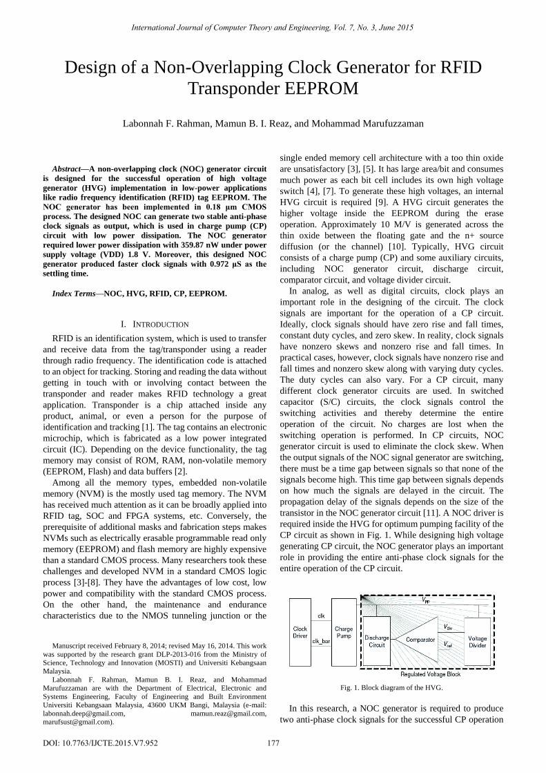
CP circuit as shown in Fig. 1. While designing high voltage
generating CP circuit, the NOC generator plays an important
role in providing the entire anti-phase clock signals for the
entire operation of the CP circuit.
Fig. 1. Block diagram of the HVG.
In this research, a NOC generator is required to produce
two anti-phase clock signals for the successful CP operation
Design of a Non-Overlapping Clock Generator for RFID
Transponder EEPROM
Labonnah F. Rahman, Mamun B. I. Reaz, and Mohammad Marufuzzaman
International Journal of Computer Theory and Engineering, Vol. 7, No. 3, June 2015
177DOI: 10.7763/IJCTE.2015.V7.952
for the implementation of the HVG. Moreover, this NOC
generator will be suitable for the functionality of the low
power applications like RFID transponder EEPROM. The
designed NOC generator is able to perform faster with lower
settling time and dissipates lower power under low power
supply voltage. In addition, the NOC generator has been
designed with the CEDEC 0.18 μm CMOS process.
II. METHODOLOGY
A NOC generator is required inside the HVG for optimum
pumping facility of the CP circuit. Generally, a clock
generator takes a clock signal and produces two-phase NOC
signals. Non-overlapping signals are signals operating at the
same frequency. None of the non-overlapping signals is high
at the time of transition from high to low or vice versa.
Generally, a clock generator takes a clock signal and
produces two-phase non-overlapping clock. The falling edge
of the input passes through the NAND gate, while the rising
edge has to propagate first through the other NAND gate and
the cascaded delay element. The resulting signals, φ and φb,
have a non-overlapping time equal to the sum of the delay at
the NAND gate of the delay element. To construct the delay
element, an even number of inverters have been used. When
driving long clock lines, additional buffer stages need to be
used to maintain sharp output clock rise and fall times [12].
Fig. 2 shows the schematic diagram of the NOC generator.
The generated clock pair CLK and CLKB is
non-overlapping. In this research, the operation of the clock
generator has two parts, where the first part contains four
standard cells from “CEDEC Std cells” library 3-x inv01a
(INV01A1, INV01A2, and INV01A4) and 1-x nand02a
(NAND02A1). In addition, the second part contains three
standard cells: 1-x nand02a (NAND02A2) and 2-x inv01a
(INV01A5 and INV01A6).
Fig. 2. Schematic diagram of the NOC generator.
When the falling edge of the input signal is passed through
the INV01A1, INV01A2 and NAND02A1 gates, it generates
a signal, which is same as the falling edge. This signal again
passes through the delay element INV01A4 and produces the
signal CLK that is in rising edge. At the same time, the rising
edge is propagating first through the other NAND02A2 gate
and the cascaded delay element. To construct the delay
element, an even number of inverters INV01A5 and
INV01A6 is used. After passing through the even number of
delay elements, the signal CLKB is generated, which is in the
falling edge. Finally, the resulting signals, CLK and CLKB,
have a non-overlapping time equal to the sum of the delay at
the NAND gates of the delay element.
The NOC generator circuit layout has been designed using
the standard cells from the “CEDEC Std cells” library. To
design the NOC generator as mentioned in the schematic
section, 5-x inv01a, 2-x nand02a are placed side by side as
shown in Fig. 3. To reduce the complexity of the design, all
logic gates are placed alongside. In addition, this placement is
required only one VDD and VSS connection and reduces the
complexity of the designs.
Input comes with MET1 from the input A of inv01a gate
(marked as 1). The output Y of this inv01a gate is connected
with the input A of the inv01a gate (marked as 2). At the same
time, another input from this point is connected with the input
A0 of the nand02a gate (marked as 5). The output Y of the
inv02a (1) is connected with the input A1 of both nand02a
gates (3 and 5). The output Y of nand02a gate (3) is added to
the input A of inv01a gate (4) through the MET2, which is
0.28 μm in width. The output Y of inv01a gate (4) is one of
the targeted outputs CLK, which is drawn using the MET3
(0.28 μm) layer to avoid the short circuit. The output Y of
nand02a gate (5) is connected to the input A of inv01a gate
(6) and the output Y is connected with the last inverter inv01a
(7). Finally, another targeted output CLKB comes from the
output Y of the inv01a gate (7).
Fig. 3. Layout for the non-overlapping clock generator.
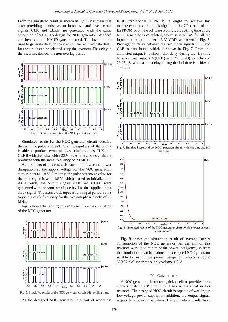
III. RESULTS AND DISCUSSION
The NOC generator circuit is designed in CEDEC 0.18 μm
CMOS process. The designed NOC circuit has been verified
by using the ELDONET simulator of the CEDEC 0.18 μm
process. Generally, output voltages (CLK and CLKB) are
with the same voltage level as the power supply voltage
(VDD). Fig. 4 shows the NOC generator test bench, where
two output signals are formed to confirm the circuit
performance.
Fig. 4. NOC generator testbench diagram.
NOC generator circuit is simulated under VDD = 1.8 V.
1 2 3 4 5 6 7
International Journal of Computer Theory and Engineering, Vol. 7, No. 3, June 2015
178
From the simulated result as shown in Fig. 5 it is clear that
after providing a pulse as an input two anti-phase clock
signals CLK and CLKB are generated with the same
amplitude of VDD. To design the NOC generator, standard
cell inverters and NAND gates are used. The inverters are
used to generate delay in the circuit. The required gate delay
for the circuit can be selected using the inverters. The delay in
the inverters decides the non-overlap period.
Fig. 5. Simulated results of the NOC generator circuit.
Simulated results for the NOC generator circuit revealed
that with the pulse width 21 nS as the input signal, the circuit
is able to produce two anti-phase clock signals CLK and
CLKB with the pulse width 20.9 nS. All the clock signals are
produced with the same frequency of 20 MHz.
As the focus of this research work is to lower the power
dissipation, so the supply voltage for the NOC generation
circuit is set to 1.8 V. Similarly, the pulse statement value for
the input signal is set to 1.8 V, which is used for initialization.
As a result, the output signals CLK and CLKB were
generated with the same amplitude level as the supplied input
clock signal. The main clock input is running at period 50 nS
to yield a clock frequency for the two anti phase clocks of 20
MHz.
Fig. 6 shows the settling time achieved from the simulation
of the NOC generator.
Fig. 6. Simulated results of the NOC generator circuit with settling time.
As the designed NOC generator is a part of readerless
RFID transponder EEPROM, it ought to achieve fast
maneuver to pass the clock signals to the CP circuit of the
EEPROM. From the software features, the settling time of the
NOC generator is calculated, which is 0.972 μS for all the
inputs and outputs under 1.8 V VDD, as shown in Fig. 7.
Propagation delay between the two clock signals CLK and
CLB is also found, which is shown in Fig. 7. From the
simulated output it is shown that delay during the rise time
between two signals V(CLK) and V(CLKB) is achieved
29.05 nS, whereas the delay during the fall time is achieved
20.82 nS.
Fig. 7. Simulated results of the NOC generator circuit with rise time and fall
time delay.
Fig. 8. Simulated results of the NOC generator circuit with average current
consumption.
Fig. 8 shows the simulation result of average current
consumption of the NOC generator. As the aim of this
research work is to minimize the power indulgence, so from
the simulation it can be claimed the designed NOC generator
is able to restrict the power dissipation, which is found
359.87 nW under the supply voltage 1.8 V.
IV. CONCLUSION
A NOC generator circuit using delay cells to provide direct
clock signals to CP circuit for HVG is presented in this
research. The designed NOC circuit is capable of working in
low-voltage power supply. In addition, the output signals
require low power dissipation. The simulation results have
International Journal of Computer Theory and Engineering, Vol. 7, No. 3, June 2015
179
shown that the designed NOC circuit with one input pulse of
20 MHz is able to generate to anti-phase non-overlapping
clock signals as the output with 1.8V power supply voltage.
In addition, the generated output signals are with the same
amplitude of VDD, which is compatible with the HVG
circuit. Thus, the designed NOC generator will be suitable for
the HVG circuit, which is required to generate high voltage
internally for NVM storage like RFID transponder
EEPROM.
ACKNOWLEDGMENT
The authors would like to express sincere gratitude to the
research grant DLP-2013-016 from the Ministry of Science,
Technology and Innovation (MOSTI) and Universiti
Kebangsaan Malaysia for supporting this research project.
REFERENCES
[1] M. J. Uddin, M. I. Ibrahimy, M. B. I. Reaz, and A. N. Nordin, “Design
and application of radio frequency identification systems,” European
Journal of Scientific Research, vol. 33, no. 3, pp. 438-453, 2009.
[2] F. M. Yasin, M. K. Khaw, and M. B. I. Reaz, “Radio Frequency
Identification: Evolution of Transponder Circuit Design,” Microwave
Journal, vol. 49, no. 6, p. 56, 2006.
[3] K. Ohsaki, N. Asamoto, and S. Takagaki, “A single poly EEPROM cell
structure for use in standard CMOS processes,” IEEE Journal of
Solid-State Circuits, vol. 29, no. 3, pp. 311-316, Mar. 1994.
[4] Z. Dixian, Y. Na, X. Wen, Y. Liwu, W. Junyu, and M. Hao, “A
low-power, single-poly, non-volatile memory for passive RFID tags,”
Chinese Journal of Semiconductors, vol. 29, pp. 99-104, Jan. 2008.
[5] B. Wang, H. Nguyen, Y. Ma, and R. Paulsen, “Highly reliable 90-nm
logic multitime programmable NVM cells using novel
work-function-engineered tunneling devices,” IEEE Transactions on
Electron Devices, vol. 54, no. 9, pp. 2526-2530, Sept. 2007.
[6] L. Rahman, M. B. I. Reaz, C. T. Gyu, and M. Marufuzzaman, “Design
of sense amplifier for non volatile memory,” Revue Roumaine Des
Sciences Techniques, vol. 58, no. 2, pp. 173–182, 2013.
[7] J. Raszka, M. Advani, V. Tiwari, L. Varisco, N. D. Hacobian, A.
Mittal, M. Han, A. Shirdel, and A. Shubat, “Embedded flash memory
for security applications in a 0.13 μm CMOS logic process,” in Proc.
International Solid-State Circuits Conference (ISSCC), IEEE, 15-19
Feb., 2004 .
[8] L. F. Rahman, M. B. I. Reaz, M. A. M. Ali, and M. Marufuzzaman,
“Implementation of sense amplifier in 0.18-μm CMOS process,”
Electronics and Electrical Engineering, vol. 120, no. 4, pp. 113-116,
2012.
[9] M. G. Mohammad, M.-J. Ahmad, and M. B. Al-Bakheet, “Switched
positive/negative charge pump design using standard CMOS
transistors,” IET Circuits Devices System, vol. 4, no. 1, pp. 57–66, Jan.
2010.
[10] IEEE Standard Definitions and Characterization of Floating Gate
Semiconductor Arrays, IEEE Std. 1005, 1999.
[11] F. Kavak, “A sizing algorithm for non-overlapping clock signal
generators,” Master thesis, Institute of Technology, Linköping
University, Sweden. Jun. 2004.
[12] F. Pan and T. Samaddar, Charge Pump Circuit Design, New York:
McGraw-Hill, 2006.
Labonnah F. Rahman was born in Bangladesh in
September 1983. She received her M.Sc. degree in
electrical, electronic and systems engineering from
Universiti Kebangsaan Malaysia, UKM Bangi,
Malaysia in 2012. Since 2007 to 2009, she worked for
GlaxoSmithKline Bangladesh Limited as an IT
systems executive. Currently she is doing her Ph.D. by
research in the area of IPv6 based RFID systems under
the Dept. of Electrical, Electronic and Systems
Engineering in UKM. Her research interests are in the following fields: IP
networking, wireless networking, data communication, microchip design
and fabrication.
M. B. I. Reaz was born in Bangladesh in December
1963. He received his B.Sc. and M.Sc. degrees in
applied physics and electronics, both from University
of Rajhashi, Bangladesh, in 1985 and 1986,
respectively. He received his D.Eng. degree in 2007
from Ibaraki University, Japan. He is currently a
professor in the Department of Electrical, Electronic
and Systems Engineering, Universiti Kebangsaan
Malaysia, Malaysia involving in teaching, research and industrial
consultation. He is a regular associate of the Abdus Salam International
Center for Theoretical Physics since 2008. He is also a senior member of
IEEE. He has vast research experiences in Norway, Ireland and Malaysia. He
has published extensively in the area of IC design and biomedical application
IC. He is author and co-author of more than 200 research articles in design
automation and IC design for biomedical applications.
Mohd. Marufuzzaman was born in Bangladesh in
June 1983. He received the M.Sc. degree in electrical,
electronic and systems engineering from Universiti
Kebangsaan Malaysia, UKM Bangi, Malaysia in
2012. Currently he is doing his Ph.D. in the Dept. of
Electrical, Electronic and Systems Engineering in
University Kebangsaan Malaysia. His research
interests are in the following fields: IP networking,
wireless networking, data communication, microchip
design and fabrication.
International Journal of Computer Theory and Engineering, Vol. 7, No. 3, June 2015
180