Design Constraints for Image-Reject Frequency-Translating Modulators
5
896 IEEE TRANSACTIONS ON CIRCUITS AND SYSTEMS—II: EXPRESS BRIEFS, VOL. 56, NO. 12, DECEMBER 2009 Design Constraints for Image-Reject Frequency-Translating ΔΣ Modulators Philip M. Chopp and Anas A. Hamoui Abstract—This brief derives design constraints for bandpass ΔΣ modulators that use mixers to perform frequency downcon- version inside their ΔΣ loop. Such systems, which are referred to as frequency-translating ΔΣ modulators, facilitate direct analog- to-digital conversion (ADC) of high-frequency signals that cannot adequately be processed using classical bandpass ΔΣ modulator architectures. The derived constraints are required for the correct design of frequency-translating ΔΣ modulators: 1) The sampling constraints maintain the stability of the ΔΣ feedback loop and prevent the mixing of the undesired signal content into the input- signal band, thereby ensuring that the time-varying behavior of the mixers does not affect the ADC resolution; and 2) the noise-shaping constraints minimize performance loss during the recombination of the in-phase and quadrature feedback paths. This brief analyzes frequency-translating ΔΣ modulators that are designed with image-reject (quadrature) mixing and that are implemented using continuous- or discrete-time lowpass or complex-bandpass inner-loop ΔΣ modulators. Thus, the derived constraints offer a valuable reference for the design of image- reject frequency-translating ΔΣ ADCs. Index Terms—Analog-to-digital (A/D) conversion, bandpass, frequency translation, sigma–delta (ΔΣ) modulation. I. I NTRODUCTION B ANDPASS ΔΣ modulation is an attractive approach for direct analog-to-digital (A/D) conversion of IF sig- nals. However, due to the technological limitations of CMOS processes and the requirement for a moderate power budget, the maximum input frequency that can be adequately processed using a classical bandpass ΔΣ modulator architecture is limited to approximately 50–60 MHz [1], [2]. To extend the advantages of ΔΣ modulation to high-frequency signals, [3] and [5] pro- posed the use of frequency downconversion inside the ΔΣ loop. These downconversion bandpass ΔΣ modulators perform noise shaping largely at baseband or at a low IF, thereby relaxing the design requirements on the ΔΣ loop filter. Downconversion bandpass ΔΣ modulators can be split into two categories: 1) frequency-translating ΔΣ modulators, which use mixing in their forward path [3], [4]; and 2) subsampling ΔΣ modulators, which use undersampling in their forward path [5]–[9]. Both architectures require upconversion mixers in their feedback path. Manuscript received June 10, 2009; revised September 1, 2009. Current version published December 16, 2009. This work was supported in part by the Natural Sciences and Engineering Research Council of Canada and the Fonds Québécois de la Recherche sur la Nature et les Technologies. This paper was recommended by Associate Editor H.-S. Chen. The authors are with the Department of Electrical and Computer En- gineering, McGill University, Montreal, QC H3A 2A7, Canada (e-mail: [email protected]). Digital Object Identifier 10.1109/TCSII.2009.2035266 Fig. 1. Frequency-translating ΔΣ modulator with image-reject (quadrature) mixing. Here, T S is the sampling period, and T D is the quadrature-path sampling delay. Frequency-translating ΔΣ modulators have two principal advantages over subsampling ΔΣ modulators: 1) They can use continuous-time (CT) loop-filter stages in their forward path following downconversion mixing, thus suppressing aliasing and sampling errors while offering greater potential for high- speed low-power design; and 2) they do not require wideband sampling switches, thus reducing both design complexity and sampled out-of-band noise. Fig. 1 depicts a block diagram of the image-reject (quadra- ture) frequency-translating ΔΣ modulator. Observe that, since the downconversion mixers are inside the ΔΣ loop, mixing nonidealities and any in-phase and quadrature path mismatch are shaped by the outer-loop bandpass filter. This filter is im- plemented using a single-stage LC resonator, which is suitable for high-frequency signal processing. When the frequency response of the outer-loop bandpass filter is translated to baseband or to a low IF, its selectivity, and hence its ability to shape quantization noise, is reduced. Therefore, additional ΔΣ loop-filter stages must be included after the downconversion mixers to enhance the overall quan- tization noise-shaping performance. These inner-loop ΔΣ modulators (Fig. 1) can be realized with lowpass or complex- bandpass loop filters to process zero- or low-IF signals. They are implemented using active-RC or switched-capacitor circuit topologies [10], which facilitate the use of switching mixers. 1549-7747/$26.00 © 2009 IEEE
Transcript of Design Constraints for Image-Reject Frequency-Translating Modulators
896 IEEE TRANSACTIONS ON CIRCUITS AND SYSTEMS—II: EXPRESS BRIEFS, VOL. 56, NO. 12, DECEMBER 2009
Design Constraints for Image-RejectFrequency-Translating ΔΣ Modulators
Philip M. Chopp and Anas A. Hamoui
Abstract—This brief derives design constraints for bandpassΔΣ modulators that use mixers to perform frequency downcon-version inside their ΔΣ loop. Such systems, which are referred toas frequency-translating ΔΣ modulators, facilitate direct analog-to-digital conversion (ADC) of high-frequency signals that cannotadequately be processed using classical bandpass ΔΣ modulatorarchitectures. The derived constraints are required for the correctdesign of frequency-translating ΔΣ modulators: 1) The samplingconstraints maintain the stability of the ΔΣ feedback loop andprevent the mixing of the undesired signal content into the input-signal band, thereby ensuring that the time-varying behaviorof the mixers does not affect the ADC resolution; and 2) thenoise-shaping constraints minimize performance loss during therecombination of the in-phase and quadrature feedback paths.This brief analyzes frequency-translating ΔΣ modulators thatare designed with image-reject (quadrature) mixing and thatare implemented using continuous- or discrete-time lowpass orcomplex-bandpass inner-loop ΔΣ modulators. Thus, the derivedconstraints offer a valuable reference for the design of image-reject frequency-translating ΔΣ ADCs.
Index Terms—Analog-to-digital (A/D) conversion, bandpass,frequency translation, sigma–delta (ΔΣ) modulation.
I. INTRODUCTION
BANDPASS ΔΣ modulation is an attractive approachfor direct analog-to-digital (A/D) conversion of IF sig-
nals. However, due to the technological limitations of CMOSprocesses and the requirement for a moderate power budget,the maximum input frequency that can be adequately processedusing a classical bandpass ΔΣ modulator architecture is limitedto approximately 50–60 MHz [1], [2]. To extend the advantagesof ΔΣ modulation to high-frequency signals, [3] and [5] pro-posed the use of frequency downconversion inside the ΔΣ loop.These downconversion bandpass ΔΣ modulators perform noiseshaping largely at baseband or at a low IF, thereby relaxing thedesign requirements on the ΔΣ loop filter.
Downconversion bandpass ΔΣ modulators can be split intotwo categories: 1) frequency-translating ΔΣ modulators, whichuse mixing in their forward path [3], [4]; and 2) subsamplingΔΣ modulators, which use undersampling in their forward path[5]–[9]. Both architectures require upconversion mixers in theirfeedback path.
Manuscript received June 10, 2009; revised September 1, 2009. Currentversion published December 16, 2009. This work was supported in part by theNatural Sciences and Engineering Research Council of Canada and the FondsQuébécois de la Recherche sur la Nature et les Technologies. This paper wasrecommended by Associate Editor H.-S. Chen.
The authors are with the Department of Electrical and Computer En-gineering, McGill University, Montreal, QC H3A 2A7, Canada (e-mail:[email protected]).
Digital Object Identifier 10.1109/TCSII.2009.2035266
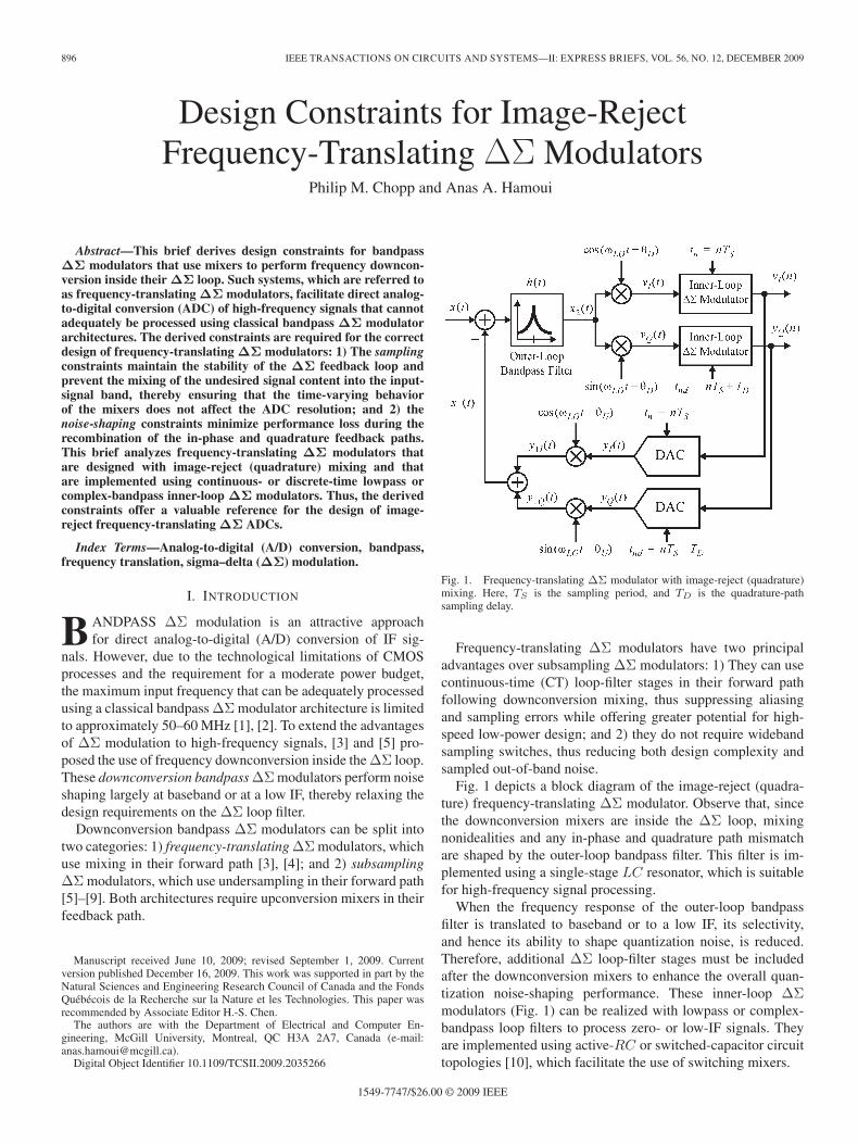
Fig. 1. Frequency-translating ΔΣ modulator with image-reject (quadrature)mixing. Here, TS is the sampling period, and TD is the quadrature-pathsampling delay.
Frequency-translating ΔΣ modulators have two principaladvantages over subsampling ΔΣ modulators: 1) They can usecontinuous-time (CT) loop-filter stages in their forward pathfollowing downconversion mixing, thus suppressing aliasingand sampling errors while offering greater potential for high-speed low-power design; and 2) they do not require widebandsampling switches, thus reducing both design complexity andsampled out-of-band noise.
Fig. 1 depicts a block diagram of the image-reject (quadra-ture) frequency-translating ΔΣ modulator. Observe that, sincethe downconversion mixers are inside the ΔΣ loop, mixingnonidealities and any in-phase and quadrature path mismatchare shaped by the outer-loop bandpass filter. This filter is im-plemented using a single-stage LC resonator, which is suitablefor high-frequency signal processing.
When the frequency response of the outer-loop bandpassfilter is translated to baseband or to a low IF, its selectivity,and hence its ability to shape quantization noise, is reduced.Therefore, additional ΔΣ loop-filter stages must be includedafter the downconversion mixers to enhance the overall quan-tization noise-shaping performance. These inner-loop ΔΣmodulators (Fig. 1) can be realized with lowpass or complex-bandpass loop filters to process zero- or low-IF signals. Theyare implemented using active-RC or switched-capacitor circuittopologies [10], which facilitate the use of switching mixers.
1549-7747/$26.00 © 2009 IEEE
CHOPP AND HAMOUI: DESIGN CONSTRAINTS FOR IMAGE-REJECT FREQUENCY-TRANSLATING ΔΣ MODULATORS 897
For the image-reject frequency-translating ΔΣ ADC, thisbrief derives the following: 1) sampling constraints, whichmaintain the stability of the ΔΣ feedback loop and preventthe mixing of the undesired signal content into the input-signal band; and 2) noise-shaping constraints, which minimizeperformance loss during the recombination of the in-phase andquadrature feedback paths.
The brief is structured as follows. Sections II and III derivethe sampling and noise-shaping constraints, respectively.Section IV then validates the derived constraints using system-level behavioral simulations in Simulink.
II. SAMPLING CONSTRAINTS
Mixers are time-varying blocks by definition. When they areinserted into the feedback loop of a ΔΣ modulator (Fig. 1),its loop response also becomes time varying. Therefore, topreserve the stability of the ΔΣ feedback loop and preventundesired signal content from mixing into the input-signalband, certain constraints must be imposed on the timing ofthe sampling instants in a frequency-translating ΔΣ modu-lator. These constraints ensure that, when sampled, the loopresponse of the frequency-translating ΔΣ modulator is effec-tively linear time invariant (LTI). A time-varying system whosesampled response is LTI is referred to as a periodically lineartime-invariant (PLTI) system [3]. Accordingly, a frequency-translating ΔΣ modulator must be a PLTI system.
Consider the frequency-translating ΔΣ modulator in Fig. 1.Define the in-phase and quadrature sampling instants as
tn = nTS and tnd = nTS + TD (1)
where TS is the sampling period, and TD is the quadrature-pathsampling delay. This section derives the general relationshipsbetween TS , TD, and the period of the local-oscillation (LO)signal TLO (in Fig. 1) that must be satisfied for correct operationof an image-reject frequency-translating ΔΣ modulator.
A. Loop Response
The sampling constraints are developed by first deriving theloop response, from y(t) to v(t), of the image-reject frequency-translating ΔΣ modulator in Fig. 1. The sampling period TS
and the quadrature-path sampling delay TD are then selected,such that the time-varying terms in this loop response aresuppressed.
Following upconversion mixing, the summed output of thein-phase and quadrature feedback paths (Fig. 1) is given by
x1(t) = yI(t) cos(ωLOt) + yQ(t) sin(ωLOt) (2)
where yI(t) and yQ(t) represent the outputs of the in-phaseand quadrature feedback digital-to-analog converters (DACs),respectively. To keep the derived results tractable, phase termsθU and θD in Fig. 1 are assumed to be 0. Furthermore, sub-sequent equations only consider the in-phase component yI(t)(i.e., yQ(t) is set to 0).
The loop response, from y(t) to v(t), is derived by setting theinput signal x(t) to 0. The output of the outer-loop filter h(t) in
Fig. 1 is then given by
x2(t) = h(t) ⊗ x1(t)
=
∞∫
−∞h(τ)yI(t − τ) cos (ωLO(t − τ)) dτ (3)
where ⊗ represents the convolution operation. By expandingthe cos(ωLO(t − τ)) term using standard trigonometric identi-ties, x2(t) can be rewritten as
x2(t) = x2I(t) cos(ωLOt) + x2Q(t) sin(ωLOt) (4)
where
x2I(t) = [h(t) cos(ωLOt)] ⊗ yI(t) (5)
x2Q(t) = [h(t) sin(ωLOt)] ⊗ yI(t). (6)
The outputs of the downconversion mixers are then given by
vI(t)=12x2I(t) [1 + cos(2ωLOt)]+
12x2Q(t) sin(2ωLOt) (7)
vQ(t)=12x2I(t) sin(2ωLOt)+
12x2Q(t) [1 − cos(2ωLOt)]. (8)
Equations (7) and (8), together with (5) and (6), give theeffective response, from y(t) to v(t), of the feedback system inFig. 1. They demonstrate that the loop response of a frequency-translating ΔΣ modulator is not LTI, due to the presence ofthe cos(2ωLOt) and sin(2ωLOt) terms. To ensure that this loopresponse is PLTI when sampled, the sampling period TS andthe quadrature-path sampling delay TD must be selected (asderived next) such that the time-varying terms remain constantacross all sampling instants.
B. Sampling and Delay Constraints
If the in-phase component vI(t) in (7) is sampled at timeinstants tn = nTS (Fig. 1), with TS set to an integer multipleof TLO/2, it reduces to vI(tn) = x2I(tn), and hence, timeinvariance is satisfied. This constraint on the sampling periodcan be generalized as
TS = kSTLO
2, kS = 1, 2, 3, . . . . (9)
If the quadrature component vQ(t) in (8) is sampled attime instants tn = nTS , with TS selected according to theconstraint given in (9), it reduces to vQ(tn) = 0 in all cases.However, since the quadrature LO signal is π/2 out-of-phasewith respect to the in-phase LO signal, delaying the quadrature-path sampling instants by TD = TLO/4 and sampling vQ(t) attime instants tnd = nTS + TD (as shown in Fig. 1) results invQ(tnd) = x2Q(tnd). Accordingly, using (9), the constraint onthe quadrature-path sampling delay can be generalized as
TD =1kS
TS
2, kS = 1, 2, 3, . . . . (10)
Observe that, when applying the constraints in (9) and (10),the ratio TD/TS decreases as TS/TLO increases (i.e., as kS
898 IEEE TRANSACTIONS ON CIRCUITS AND SYSTEMS—II: EXPRESS BRIEFS, VOL. 56, NO. 12, DECEMBER 2009
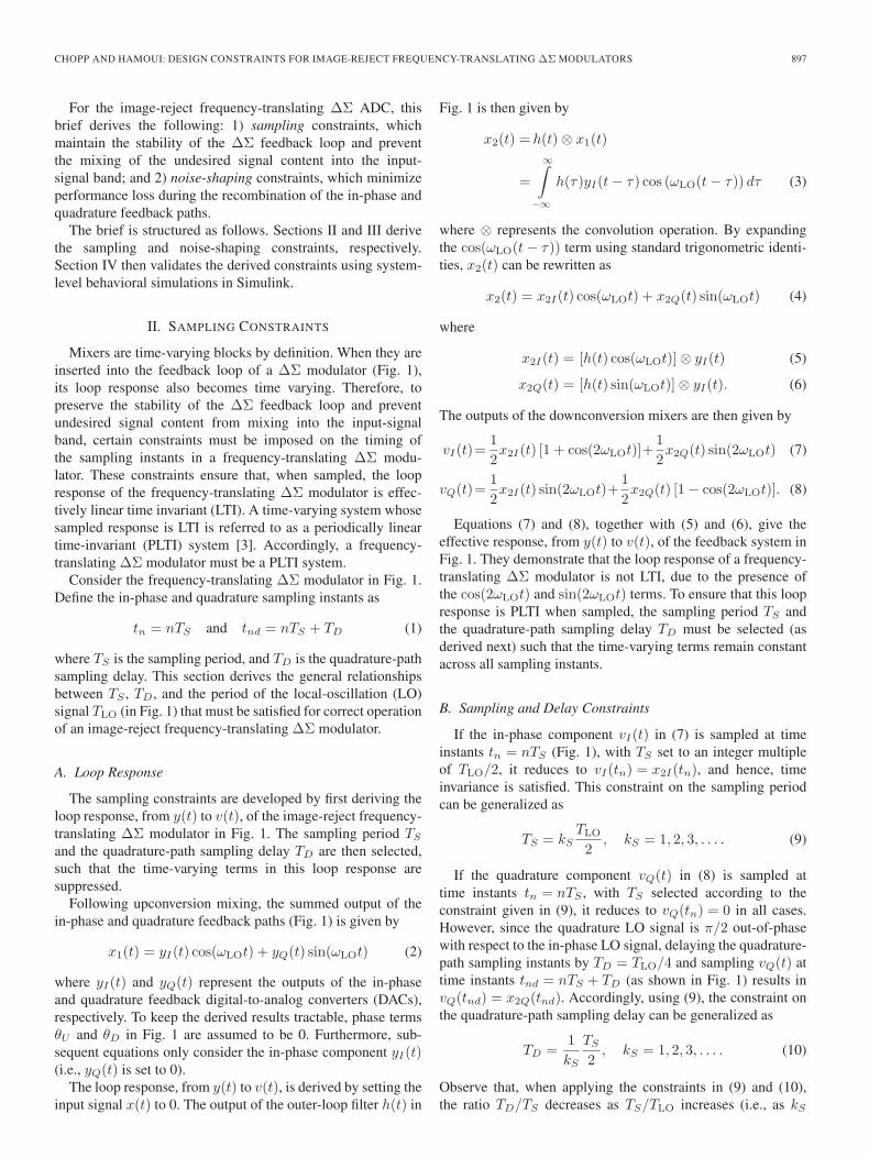
Fig. 2. Timing of the quadrature-path sampling instants tnd for TD = TS/2 and: (a) TS = TLO/2; (b) TS = TLO; and (c) TS = 3TLO/2.
increases), thereby making it increasingly difficult to accuratelyimplement TD. To solve this problem, the constraint in (9) isrevised in the following discussion, such that TD scales withTLO. This makes it possible to adjust TS/TLO without affectingTD/TS .
Let the quadrature-path sampling delay be fixed atTD = TS/2. Consider the case where the sampling period isTS = TLO/2 [i.e., for kS = 1 in (9)]. At the quadrature-pathsampling instants tnd = nTS + TD, cos(2ωLOtnd) = −1 andsin(2ωLOtnd) = 0, resulting in vQ(tnd) = x2Q(tnd) in (8).Fig. 2(a) plots the cos(2ωLOt) curve, marking the positionsof the quadrature-path sampling instants tnd for TS = TLO/2and TD = TS/2. In Fig. 2(b) and (c), TS is increased bymultiples of TLO/2, whereas TD is fixed at TS/2. Note thatsin(2ωLOtnd) = 0 in Fig. 2(b) and (c). In Fig. 2(b) (i.e., forTS = TLO), cos(2ωLOtnd) = 1, and hence, vQ(tnd) in (8)reduces to 0, which is incorrect. However, in Fig. 2(c) (i.e.,for TS = 3TLO/2), cos(2ωLOtnd) = −1, and hence, vQ(tnd)in (8) reduces to x2Q(tnd), which is the correct result. There-fore, when TD = TS/2, vQ(tnd) is nonzero, and time invari-ance is correctly maintained only when the sampling period TS
is an odd multiple of TLO/2. This result can be generalized byintroducing an additional design factor kD into the samplingconstraint in (9) as follows:
TS =kDkSTLO
2, kD =1, 3, 5, . . . ; kS =1, 2, 3, . . . . (11)
Using (11), the constraint on the quadrature-path samplingdelay in (10) can be rewritten as
TD = kDTLO
4, kD = 1, 3, 5, . . . . (12)
Accordingly, the sampling period TS of an image-rejectfrequency-translating ΔΣ modulator (Fig. 1) must be selectedusing (11), and the quadrature-path sampling instants must bedelayed by TD according to (12).
It is important to point out that the sampling constraintsin (11) and (12) have been derived independent of the noisetransfer function (NTF) of the inner-loop ΔΣ modulators and,therefore, can be applied to design image-reject frequency-translating ΔΣ modulators with continous-time (CT) ordiscrete-time (DT) lowpass or complex-bandpass inner-loopΔΣ modulators. However, note that a complex-bandpass inner-loop ΔΣ modulator cannot be implemented with a DT loopfilter, since the cross-coupled feedback paths of the complex
integrators cannot be realized when the sampling instants of thein-phase and quadrature paths have different delays.
C. DT Versus CT Inner-Loop ΔΣ Modulators
In Fig. 1, the outputs of the downconversion mixers containboth a low-frequency term (close to dc) and a high-frequencyterm (close to 2ωLO). Using DT inner-loop ΔΣ modulators [3],the in-phase and quadrature paths are sampled immediately fol-lowing downconversion mixing, and the high-frequency termis subsampled to baseband. The quadrature-path sampling in-stants must therefore be delayed by TD relative to the in-phasepath sampling instants [as per the constraint in (12)], to avoidcancellation of the low-frequency term by the subsampled high-frequency term.
In a frequency-translating ΔΣ modulator with CT inner-loopΔΣ modulators [4], the high-frequency term is filtered by thesignal transfer function of the CT inner-loop ΔΣ modulatorsand is attenuated prior to sampling. This implicit filtering makesit possible to realize an image-reject frequency-translating ΔΣmodulator with TD = 0 (i.e., with the in-phase and quadraturepaths sampled at the same time instants), where the samplingperiod TS is constrained by (9), rather than (11).
D. General LO Signals
The sampling constraints in (11) and (12) have been derivedassuming that the LO signals have the same phase as thesampling clock (i.e., θU = 0 and θD = 0 in Fig. 1). To verifythat (11) and (12) are valid beyond this particular case, theseconstraints are applied to the outputs of the downconversionmixers, assuming that the LO signals have general phases θU
and θD (Fig. 1). At sampling instants, this results in
vI(tn)= cos(θD)[cos(θU )x2I(tn) + sin(θU )x2Q(tn)] (13)
vQ(tnd)= cos(θD)[cos(θU )x2Q(tnd) − sin(θU )x2I(tnd)] .
(14)
As per (13) and (14), the sampled outputs of the downcon-version mixers remain time invariant but now depend on phasesθU and θD. The phase θU of the LO signal that is applied tothe upconversion mixers alters the response through the outer-loop path [6], whereas the phase θD that is applied to thedownconversion mixer simply acts as a scaling factor.
CHOPP AND HAMOUI: DESIGN CONSTRAINTS FOR IMAGE-REJECT FREQUENCY-TRANSLATING ΔΣ MODULATORS 899
A nonsinusoidal LO signal (e.g., the square wave generatedby a switching mixer) introduces harmonics of the basebandspectrum at multiples of the LO frequency. When a nonsi-nusoidal LO signal is applied to the downconversion mixers,its harmonics are either subsampled (for DT inner-loop ΔΣmodulators) or attenuated (for CT inner-loop ΔΣ modulators)and, hence, have the same effect as a scaling factor. When anonsinusoidal LO signal is applied to the upconversion mixers,its harmonics change the effective response through the outer-loop path. However, this change can be accounted for in theloop-filter design in the same way that an arbitrary DAC pulseshape is incorporated into the design of a classical CT ΔΣmodulator. Accordingly, the observations that were previouslymade for sinusoidal LO signals with arbitrary phase terms canbe extended to general LO signals.
Observe that errors in the LO signals affect the NTF ofa frequency-translating ΔΣ modulator in the same way thatcoefficient errors affect the NTF of a classical ΔΣ modulator.The impact of such errors, on the performance and stability of afrequency-translating ΔΣ modulator, becomes more significantas its out-of-band NTF gain is increased.
III. NOISE-SHAPING CONSTRAINTS
For stable operation, a ΔΣ modulator must be designedsuch that the signal content of its input can be adequatelyreplicated by the signal content of its feedback path. This meansthat the low-frequency signal at the output of a frequency-translating ΔΣ modulator (Fig. 1) must be upconverted intothe same band as the high-frequency signal at its input. Thisupconversion, as well as subsequent in-phase and quadraturepath recombination at the input of the frequency-translating ΔΣmodulator, imposes basic constraints on the NTF of its inner-loop ΔΣ modulators, as described below.
A. Lowpass Inner-Loop ΔΣ Modulators
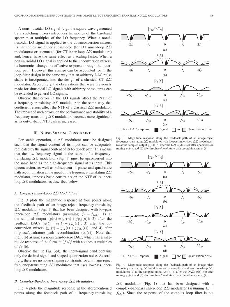
Fig. 3 plots the magnitude response at four points alongthe feedback path of an image-reject frequency-translatingΔΣ modulator (Fig. 1) that has been designed with lowpassinner-loop ΔΣ modulators (assuming fS = fLO): 1) atthe sampled output (y(n) = yI(n) + jyQ(n)); 2) after thefeedback DACs (y(t) = yI(t) + jyQ(t)); 3) after the up-conversion mixers (y1(t) = y1I(t) + jy1Q(t)); and 4) afterin-phase/quadrature path recombination (x1(t)). Note thatFig. 3(b) assumes a nonreturn-to-zero DAC, which has a mag-nitude response of the form sin(f)/f with notches at multiplesof fS [6].
Observe that, in Fig. 3(d), the input-signal band containsonly the desired signal and shaped quantization noise. Accord-ingly, there are no noise-shaping constraints for an image-rejectfrequency-translating ΔΣ modulator that uses lowpass inner-loop ΔΣ modulators.
B. Complex-Bandpass Inner-Loop ΔΣ Modulators
Fig. 4 plots the magnitude response at the aforementionedpoints along the feedback path of a frequency-translating
Fig. 3. Magnitude response along the feedback path of an image-rejectfrequency-translating ΔΣ modulator with lowpass inner-loop ΔΣ modulators:(a) at the sampled output y(n); (b) after the DACs y(t); (c) after upconversionmixing y1(t); and (d) after in-phase/quadrature path recombination x1(t).
Fig. 4. Magnitude response along the feedback path of an image-rejectfrequency-translating ΔΣ modulator with a complex-bandpass inner-loop ΔΣmodulator: (a) at the sampled output y(n); (b) after the DACs y(t); (c) aftermixing y1(t); and (d) after in-phase/quadrature path recombination x1(t).
ΔΣ modulator (Fig. 1) that has been designed with acomplex-bandpass inner-loop ΔΣ modulator (assuming fS =fLO). Since the response of the complex loop filter is not
900 IEEE TRANSACTIONS ON CIRCUITS AND SYSTEMS—II: EXPRESS BRIEFS, VOL. 56, NO. 12, DECEMBER 2009
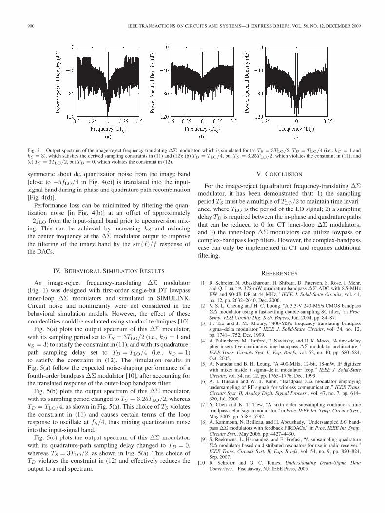
Fig. 5. Output spectrum of the image-reject frequency-translating ΔΣ modulator, which is simulated for (a) TS = 3TLO/2, TD = TLO/4 (i.e., kD = 1 andkS = 3), which satisfies the derived sampling constraints in (11) and (12); (b) TD = TLO/4, but TS = 3.25TLO/2, which violates the constraint in (11); and(c) TS = 3TLO/2, but TD = 0, which violates the constraint in (12).
symmetric about dc, quantization noise from the image band[close to −5fLO/4 in Fig. 4(c)] is translated into the input-signal band during in-phase and quadrature path recombination[Fig. 4(d)].
Performance loss can be minimized by filtering the quan-tization noise [in Fig. 4(b)] at an offset of approximately−2fLO from the input-signal band prior to upconversion mix-ing. This can be achieved by increasing kS and reducingthe center frequency at the ΔΣ modulator output to improvethe filtering of the image band by the sin(f)/f response ofthe DACs.
IV. BEHAVIORAL SIMULATION RESULTS
An image-reject frequency-translating ΔΣ modulator(Fig. 1) was designed with first-order single-bit DT lowpassinner-loop ΔΣ modulators and simulated in SIMULINK.Circuit noise and nonlinearity were not considered in thebehavioral simulation models. However, the effect of thesenonidealities could be evaluated using standard techniques [10].
Fig. 5(a) plots the output spectrum of this ΔΣ modulator,with its sampling period set to TS = 3TLO/2 (i.e., kD = 1 andkS = 3) to satisfy the constraint in (11), and with its quadrature-path sampling delay set to TD = TLO/4 (i.e., kD = 1)to satisfy the constraint in (12). The simulation results inFig. 5(a) follow the expected noise-shaping performance of afourth-order bandpass ΔΣ modulator [10], after accounting forthe translated response of the outer-loop bandpass filter.
Fig. 5(b) plots the output spectrum of this ΔΣ modulator,with its sampling period changed to TS = 3.25TLO/2, whereasTD = TLO/4, as shown in Fig. 5(a). This choice of TS violatesthe constraint in (11) and causes certain terms of the loopresponse to oscillate at fS/4, thus mixing quantization noiseinto the input-signal band.
Fig. 5(c) plots the output spectrum of this ΔΣ modulator,with its quadrature-path sampling delay changed to TD = 0,whereas TS = 3TLO/2, as shown in Fig. 5(a). This choice ofTD violates the constraint in (12) and effectively reduces theoutput to a real spectrum.
V. CONCLUSION
For the image-reject (quadrature) frequency-translating ΔΣmodulator, it has been demonstrated that: 1) the samplingperiod TS must be a multiple of TLO/2 to maintain time invari-ance, where TLO is the period of the LO signal; 2) a samplingdelay TD is required between the in-phase and quadrature pathsthat can be reduced to 0 for CT inner-loop ΔΣ modulators;and 3) the inner-loop ΔΣ modulators can utilize lowpass orcomplex-bandpass loop filters. However, the complex-bandpasscase can only be implemented in CT and requires additionalfiltering.
REFERENCES
[1] R. Schreier, N. Abaskharoun, H. Shibata, D. Paterson, S. Rose, I. Mehr,and Q. Luu, “A 375-mW quadrature bandpass ΔΣ ADC with 8.5-MHzBW and 90-dB DR at 44 MHz,” IEEE J. Solid-State Circuits, vol. 41,no. 12, pp. 2632–2640, Dec. 2006.
[2] V. S. L. Cheung and H. C. Luong, “A 3.3-V 240-MS/s CMOS bandpassΣΔ modulator using a fast-settling double-sampling SC filter,” in Proc.Symp. VLSI Circuits Dig. Tech. Papers, Jun. 2004, pp. 84–87.
[3] H. Tao and J. M. Khoury, “400-MS/s frequency translating bandpasssigma–delta modulator,” IEEE J. Solid-State Circuits, vol. 34, no. 12,pp. 1741–1752, Dec. 1999.
[4] A. Pulincherry, M. Hufford, E. Naviasky, and U. K. Moon, “A time-delayjitter-insensitive continuous-time bandpass ΔΣ modulator architecture,”IEEE Trans. Circuits Syst. II, Exp. Briefs, vol. 52, no. 10, pp. 680–684,Oct. 2005.
[5] A. Namdar and B. H. Leung, “A 400-MHz, 12-bit, 18-mW, IF digitizerwith mixer inside a sigma–delta modulator loop,” IEEE J. Solid-StateCircuits, vol. 34, no. 12, pp. 1765–1776, Dec. 1999.
[6] A. I. Hussein and W. B. Kuhn, “Bandpass ΣΔ modulator employingundersampling of RF signals for wireless communication,” IEEE Trans.Circuits Syst. II, Analog Digit. Signal Process., vol. 47, no. 7, pp. 614–620, Jul. 2000.
[7] Y. Chen and K. T. Tiew, “A sixth-order subsampling continuous-timebandpass delta–sigma modulator,” in Proc. IEEE Int. Symp. Circuits Syst.,May 2005, pp. 5589–5592.
[8] A. Kammoun, N. Beilleau, and H. Aboushady, “Undersampled LC band-pass ΔΣ modulators with feedback FIRDACs,” in Proc. IEEE Int. Symp.Circuits Syst., May 2006, pp. 4427–4430.
[9] S. Reekmans, L. Hernandez, and E. Prefasi, “A subsampling quadratureΣΔ modulator based on distributed resonators for use in radio receiver,”IEEE Trans. Circuits Syst. II, Exp. Briefs, vol. 54, no. 9, pp. 820–824,Sep. 2007.
[10] R. Schreier and G. C. Temes, Understanding Delta–Sigma DataConverters. Piscataway, NJ: IEEE Press, 2005.


![A Novel Digital Calibration Technique for Gain and Offset ......ΣΔ modulators. The input signal x[n] is distributed among the M modulators through an analog multiplexer. Then, the](https://static.fdocument.org/doc/165x107/60ee77b99c0fd85f564bb9e6/a-novel-digital-calibration-technique-for-gain-and-offset-modulators.jpg)