DC1938B – LTC3350EUHF, High Current … BACKUP •t BACKUP nηV CELL(MAX) 2 • αB + αB –...
16
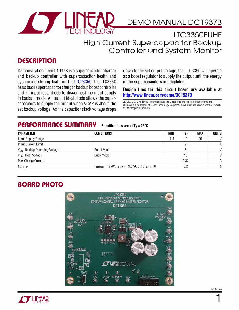
1 dc1937bfa DEMO MANUAL DC1937B DESCRIPTION LTC3350EUHF High Current Supercapacitor Backup Controller and System Monitor Demonstration circuit 1937B is a supercapacitor charger and backup controller with supercapacitor health and system monitoring; featuring the LTC ® 3350. The LTC3350 has a buck supercapacitor charger, backup boost controller and an input ideal diode to disconnect the input supply in backup mode. An output ideal diode allows the super- capacitors to supply the output when VCAP is above the set backup voltage. As the capacitor stack voltage drops L, LT, LTC, LTM, Linear Technology and the Linear logo are registered trademarks and QuikEval is a trademark of Linear Technology Corporation. All other trademarks are the property of their respective owners. PERFORMANCE SUMMARY down to the set output voltage, the LTC3350 will operate as a boost regulator to supply the output until the energy in the supercapacitors are depleted. Design files for this circuit board are available at http://www.linear.com/demo/DC1937B Specifications are at T A = 25°C PARAMETER CONDITIONS MIN TYP MAX UNITS Input Supply Range 10.8 12 20 V Input Current Limit 2 A V OUT Backup Operating Voltage Boost Mode 6 V V CAP Float Voltage Buck Mode 10 V Max Charge Current 5.33 A t BACKUP P BACKUP = 25W, I BOOST = 9.67A, 3 ≤ V CAP ≤ 10 3.2 s BOARD PHOTO
Transcript of DC1938B – LTC3350EUHF, High Current … BACKUP •t BACKUP nηV CELL(MAX) 2 • αB + αB –...
1dc1937bfa
DEMO MANUAL DC1937B
Description
LTC3350EUHFHigh Current Supercapacitor Backup
Controller and System Monitor
Demonstration circuit 1937B is a supercapacitor charger and backup controller with supercapacitor health and system monitoring; featuring the LTC®3350. The LTC3350 has a buck supercapacitor charger, backup boost controller and an input ideal diode to disconnect the input supply in backup mode. An output ideal diode allows the super-capacitors to supply the output when VCAP is above the set backup voltage. As the capacitor stack voltage drops
L, LT, LTC, LTM, Linear Technology and the Linear logo are registered trademarks and QuikEval is a trademark of Linear Technology Corporation. All other trademarks are the property of their respective owners.
performance summary
down to the set output voltage, the LTC3350 will operate as a boost regulator to supply the output until the energy in the supercapacitors are depleted.
Design files for this circuit board are available at http://www.linear.com/demo/DC1937B
Specifications are at TA = 25°C
PARAMETER CONDITIONS MIN TYP MAX UNITSInput Supply Range 10.8 12 20 V
Input Current Limit 2 A
VOUT Backup Operating Voltage Boost Mode 6 V
VCAP Float Voltage Buck Mode 10 V
Max Charge Current 5.33 A
tBACKUP PBACKUP = 25W, IBOOST = 9.67A, 3 ≤ VCAP ≤ 10 3.2 s
BoarD photo
2dc1937bfa
DEMO MANUAL DC1937B
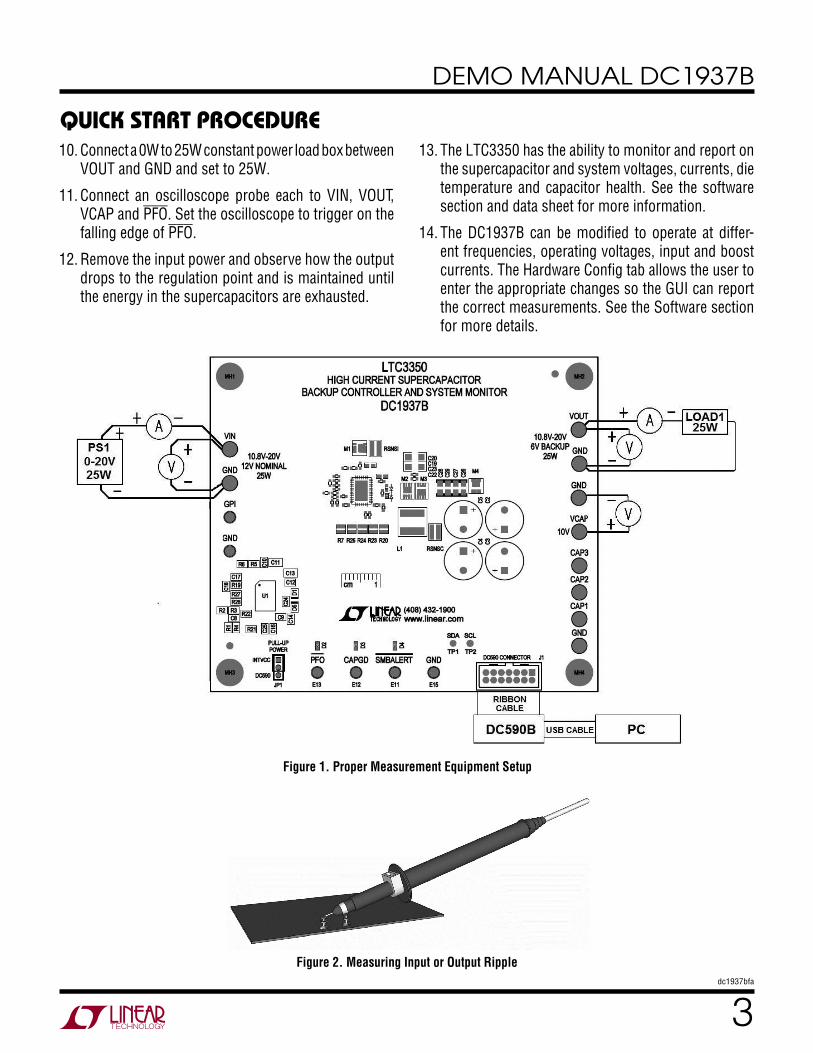
Quick start proceDureObtain and connect a DC590B board to the DC1937B board. Using short twisted pair leads for the power connections and with the LOAD and the power supply OFF. Refer to Figure 1 and Figure 2 for the proper measurement and equipment setup. Follow the procedure below.
1. Refer to the DC590B Quick Start Guide for QuikEval™ setup and software installation details.
2. Make sure the USB cable is connected between the computer and the DC590B controller board.
3. Connect a 14-pin ribbon cable from the DC590B board to the DC1937B board.
4. Set the VCCIO jumper, JP6, on the DC590B board to the 5V position.
5. Set the JP1 jumper on the DC1937B board to the DC590 position.
6. Start the Linear Technology QuikEval program. This program should automatically detect the presence of the LTC3350 demo board (DC1937B) and activate the appropriate GUI, as seen in Figure 5.
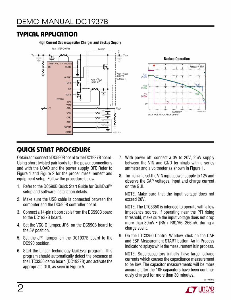
typical applicationHigh Current Supercapacitor Charger and Backup Supply
Backup OperationVIN
PFI OUTFB
OUTFET
TGATE
SW
BGATE
ICAPVCAPCAP4
CAP3
CAP2
CAP1
CAPRTN
CAPFB
INFET VOUTSP VOUTSN
ICHG (STEP-DOWN) IBACKUP
VCAP < VOUT(STEP-UP)
VCAP > VOUT(DIRECTCONNECT)
VOUT
LTC3350
10FVCAP
10F
10F
10F
dc1937b TA01a
I2C
VIN2V/DIV
VCAP2V/DIV
VOUT2V/DIV
400ms/DIVBACK PAGE APPLICATION CIRCUIT
0V
dc1937b TA01b
PBACKUP = 25W
VOUT
VCAP
VIN
7. With power off, connect a 0V to 20V, 25W supply between the VIN and GND terminals with a series ammeter and a voltmeter as shown in Figure 1.
8. Turn on and set the VIN input power supply to 12V and observe the CAP voltages, input and charge current on the GUI.
NOTE. Make sure that the input voltage does not exceed 20V.
NOTE. The LTC3350 is intended to operate with a low impedance source. If operating near the PFI rising threshold, make sure the input voltage does not drop more than 30mV • (R5 + R6)/R6, 266mV, during a charge event.
9. On the LTC3350 Control Window, click on the CAP and ESR Measurement START button. An In Process indicator displays while the measurement is in process.
NOTE. Supercapacitors initially have large leakage currents which causes the capacitance measurement to be low. The capacitor measurements will be more accurate after the 10F capacitors have been continu-ously charged for more than 30 minutes.
3dc1937bfa
DEMO MANUAL DC1937B
10. Connect a 0W to 25W constant power load box between VOUT and GND and set to 25W.
11. Connect an oscilloscope probe each to VIN, VOUT, VCAP and PFO. Set the oscilloscope to trigger on the falling edge of PFO.
12. Remove the input power and observe how the output drops to the regulation point and is maintained until the energy in the supercapacitors are exhausted.
Quick start proceDure13. The LTC3350 has the ability to monitor and report on
the supercapacitor and system voltages, currents, die temperature and capacitor health. See the software section and data sheet for more information.
14. The DC1937B can be modified to operate at differ-ent frequencies, operating voltages, input and boost currents. The Hardware Config tab allows the user to enter the appropriate changes so the GUI can report the correct measurements. See the Software section for more details.
Figure 1. Proper Measurement Equipment Setup
Figure 2. Measuring Input or Output Ripple
4dc1937bfa
DEMO MANUAL DC1937B
application information
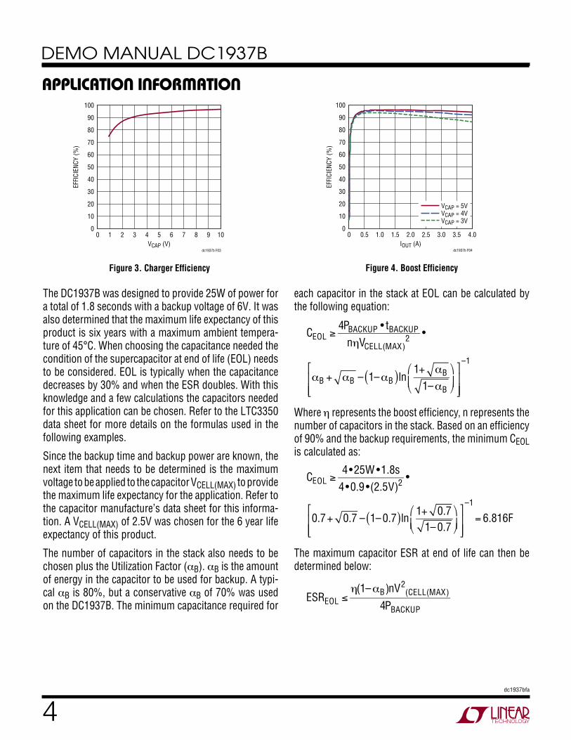
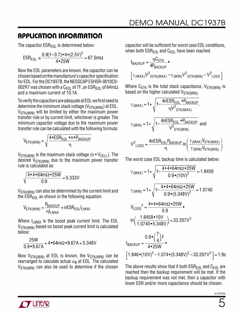
Figure 3. Charger Efficiency Figure 4. Boost Efficiency
VCAP (V)0
EFFI
CIEN
CY (%
)
100
10
90
70
50
30
80
60
40
20
05 93 7
dc1937b F03
104 82 61IOUT (A)
0
EFFI
CIEN
CY (%
)
100
10
90
70
50
30
80
60
40
20
01.5 3.50.5 2.5
dc1937b F04
4.01.0 3.02.0
VCAP = 5VVCAP = 4VVCAP = 3V
The DC1937B was designed to provide 25W of power for a total of 1.8 seconds with a backup voltage of 6V. It was also determined that the maximum life expectancy of this product is six years with a maximum ambient tempera-ture of 45°C. When choosing the capacitance needed the condition of the supercapacitor at end of life (EOL) needs to be considered. EOL is typically when the capacitance decreases by 30% and when the ESR doubles. With this knowledge and a few calculations the capacitors needed for this application can be chosen. Refer to the LTC3350 data sheet for more details on the formulas used in the following examples.
Since the backup time and backup power are known, the next item that needs to be determined is the maximum voltage to be applied to the capacitor VCELL(MAX) to provide the maximum life expectancy for the application. Refer to the capacitor manufacture’s data sheet for this informa-tion. A VCELL(MAX) of 2.5V was chosen for the 6 year life expectancy of this product.
The number of capacitors in the stack also needs to be chosen plus the Utilization Factor (αB). αB is the amount of energy in the capacitor to be used for backup. A typi-cal αB is 80%, but a conservative αB of 70% was used on the DC1937B. The minimum capacitance required for
each capacitor in the stack at EOL can be calculated by the following equation:
CEOL ≥4PBACKUP • tBACKUP
nηVCELL(MAX)2 •
αB + αB – 1– αB( )ln 1+ αB
1– αB
⎛
⎝⎜
⎞
⎠⎟
⎡
⎣⎢⎢
⎤
⎦⎥⎥
–1
Where η represents the boost efficiency, n represents the number of capacitors in the stack. Based on an efficiency of 90% and the backup requirements, the minimum CEOL is calculated as:
CEOL ≥4 •25W •1.8s
4 •0.9 •(2.5V)2 •
0.7+ 0.7 – 1– 0.7( )ln 1+ 0.71– 0.7
⎛
⎝⎜⎞
⎠⎟⎡
⎣⎢⎢
⎤
⎦⎥⎥
–1
= 6.816F
The maximum capacitor ESR at end of life can then be determined below:
ESREOL ≤
η(1– αB)nV2(CELL(MAX)
4PBACKUP
5dc1937bfa
DEMO MANUAL DC1937B
The capacitor ESREOL is determined below:
ESREOL ≤
0.9(1– 0.7)•4 •(2.5V)2
4 •25W= 67.5mΩ
Now the EOL parameters are known, the capacitor can be chosen based on the manufacture’s capacitor specification for EOL. For the DC1937B, the NESSCAP ESHSR-0010C0-002R7 was chosen with a CEOL of 7F, an ESREOL of 64mΩ and a maximum current of 10.1A.
To verify the capacitors are adequate at EOL we first need to determine the minimum stack voltage (VSTK(MIN)) at EOL. VSTK(MIN) will be limited by either the maximum power transfer rule or by current limit, whichever is greater. The minimum capacitor voltage due to the maximum power transfer rule can be calculated with the following formula:
VSTK(MIN) =
4 •ESREOL •n •PBACKUPη
VSTK(MIN) is the maximum stack voltage (n • VCELL). The desired VSTK(MIN) due to the maximum power transfer rule is calculated as:
4 •4 •64mΩ •25W0.9
= 5.333V
VSTK(MIN) can also be determined by the current limit and the ESREOL as shown in the following equation:
VSTK(MIN) =
PBACKUPηILMAX
+nESREOLILMAX
Where ILMAX is the boost peak current limit. The EOL VSTK(MIN) based on boost peak current limit is calculated below:
25W0.9 •9.67A
+ 4 •64mΩ •9.67A = 5.348V
Now VSTK(MIN) at EOL is known, the VSTK(MIN) can be rearranged to calculate actual αB at EOL. The calculated VSTK(MIN) can also be used to determine if the chosen
capacitor will be sufficient for worst case EOL conditions, when both ESREOL and CEOL have been reached.
tBACKUP =ηCSTK
4PBACKUP•
γ (MAX)V2
(STK(MAX) – γ (MIN)V2
(STK(MIN) – V2LOSS⎡
⎣⎤⎦
Where CSTK is the total stack capacitance, VSTK(MIN) is based on the higher calculated VSTK(MIN),
γ (MAX) = 1+ 1–4nESREOL •PBACKUP
ηV2STK(MAX)
,
γ (MIN) = 1+ 1–4nESREOL •PBACKUP
V2STK(MIN)
and
V2
LOSS =4nESREOLPBACKUP
ηln
γ (MAX)VSTK(MAX)
γ (MIN)VSTK(MIN)
⎛
⎝⎜
⎞
⎠⎟
The worst case EOL backup time is calculated below:
γ (MAX) = 1+ 1–
4 •4 •64mΩ •25W0.9 •(10V)2 = 1.8459
γ (MIN) = 1+ 1–
4 •4 •64mΩ •25W0.9 •(5.348V)2 = 1.0740
VLOSS2 =
4 •4 •64mΩ •25W0.9
•
ln1.8459 •10V
1.0740 •5.348V⎛⎝⎜
⎞⎠⎟
= 33.207V2
tBACKUP =0.9 •
74
⎛⎝⎜
⎞⎠⎟
F
4 •25W•
1.846 •(10V)2 –1.074 •(5.348V)2 – 33.207V2⎡⎣
⎤⎦ = 1.9s
The above results show that if both ESREOL and CEOL are reached then the backup requirement will be met. If the backup requirement was not met, then a capacitor with lower ESR and/or more capacitance should be chosen.
application information
6dc1937bfa
DEMO MANUAL DC1937B
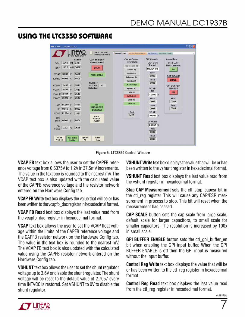
usinG the ltc3350 softWareThe LTC3350 program provides the ability to measure and monitor the system voltages and currents plus the health of the supercapacitors. It also allows the user to set up alarms to report on specific events such as power fail or cap measurement done. Refer to Figure 5 for an illustration of the LTC3350 control window.
VIEW LTC3350 PRODUCT PAGE button opens an Internet browser and searches the Linear Technology Corporation website for information on the LTC3350 when an Internet connection is available.
CAP and ESR Measurement START button starts a ca-pacitor and ESR measurement. An indicator below the START button indicates the status of the capacitor/ESR measurement. The different states are; In Process, Done, Pending or Failed.
Number of Caps Selected text box indicates the number of capacitors selected using the CAP_SLCTx pins.
SMBALERT Detected indicator indicates if an SMBALERT has been detected or not.
Clear SMBUS ALERT button sends an SMBus alert re-sponse address to clear the SMBALERT. Note, the condition that caused the SMBALERT must be cleared before the SMBALERT signal can be cleared.
CAP text box indicates the latest measured capacitance in Farads for large capacitors and mF for smaller capacitors. This measurement is based on the CAP scale setting in the control register plus the Current and Oscillator Resistor Settings on the Hardware Config tab.
ESR text box indicates the latest measured ESR in mΩ.
VCAP text box indicates the latest VCAP voltage in Volts.
ICHRG text box indicates the latest measured charge/boost current in amps. This measurement is based on the RSNSC setting on the Hardware Config tab.
VCAPx text box indicates the latest measured capacitor voltage in Volts for the corresponding VCAP.
VIN text box indicates the latest measured input voltage in Volts.
IIN text box indicates the latest measured input current in amps. This measurement is based on the RSNSI setting on the Hardware Config tab.
VOUT text box indicates the latest measured VOUT in Volts.
GPImon text box indicates the latest measured GPI voltage in Volts. An internal buffer can be enabled for measuring high impedance inputs.
Die Temp text box displays the latest internally measured die temperature in °C.
Register text boxes displays the associated register values in hexadecimal format.
Read Values button causes the LTC3350 to read all of the ADC measured values. This is useful when the LTC3350 GUI “Auto Update” is disabled.
Auto Update Enable/Disable button causes the LTC3350 to read all of the LTC3350 registers periodically and writes to any register changed when enabled. The Read Values, Read All, or Update All buttons can be used instead to update the registers when in the disabled state.
Read All button causes the LTC3350 to read all of the LTC3350 registers. This is useful when the LTC3350 GUI Auto Update is disabled.
CHARGER CONTROL TAB
The Charger Control tab contains the indicators and con-trols for the capacitor charger and monitor plus the GPI buffer enable as shown in Figure 5.
Charger Status STATUS Bits indicates when the associated chrg_status register bits are set. See the data sheet from more information on these bits.
Charger Status Read text box displays the last read chrg_status register value in hexadecimal format.
CAP ESR Period text box allows the user to set a period in which the LTC3350 will perform a capacitance and ESR measurement. The text box is formatted in hours, minutes, and seconds. The LSB for the CAP ESR Period register is 10 seconds.
CAP ESR Period Write text box displays the value that will be or has been written to the cap_esr_period register value in hexadecimal format.
CAP ESR Period Read text box displays the last value read from the cap_esr_period register in hexadecimal format.
7dc1937bfa
DEMO MANUAL DC1937B
usinG the ltc3350 softWare
Figure 5. LTC3350 Control Window
VCAP FB text box allows the user to set the CAPFB refer-ence voltage from 0.6375V to 1.2V in 37.5mV increments. The value in the text box is rounded to the nearest mV. The VCAP text box is also updated with the calculated value of the CAPFB reverence voltage and the resistor network entered on the Hardware Config tab.
VCAP FB Write text box displays the value that will be or has been written to the vcapfb_dac register in hexadecimal format.
VCAP FB Read text box displays the last value read from the vcapfb_dac register in hexadecimal format.
VCAP text box allows the user to set the VCAP float volt-age within the limits of the CAPFB reference voltage and the CAPFB resistor network on the Hardware Config tab. The value in the text box is rounded to the nearest mV. The VCAP FB text box is also updated with the calculated value using the CAPFB resistor network entered on the Hardware Config tab.
VSHUNT text box allows the user to set the shunt regulator voltage up to 3.6V or disable the shunt regulator. The shunt voltage will be reset to the default value of 2.7057 every time INTVCC is restored. Set VSHUNT to 0V to disable the shunt regulator.
VSHUNT Write text box displays the value that will be or has been written to the vshunt register in hexadecimal format.
VSHUNT Read text box displays the last value read from the vshunt register in hexadecimal format.
Stop CAP Measurement sets the ctl_stop_capesr bit in the ctl_reg register. This will cause any CAP/ESR mea-surement in process to stop. This bit will reset when the measurement has ceased.
CAP SCALE button sets the cap scale from large scale, default scale for larger capacitors, to small scale for smaller capacitors. The resolution is increased by 100x in small scale.
GPI BUFFER ENABLE button sets the ctl_gpi_buffer_en bit when enabling the GPI input buffer. When the GPI BUFFER ENABLE is off then the GPI input is measured without the input buffer.
Control Reg Write text box displays the value that will be or has been written to the ctl_reg register in hexadecimal format.
Control Reg Read text box displays the last value read from the ctl_reg register in hexadecimal format.
8dc1937bfa
DEMO MANUAL DC1937B
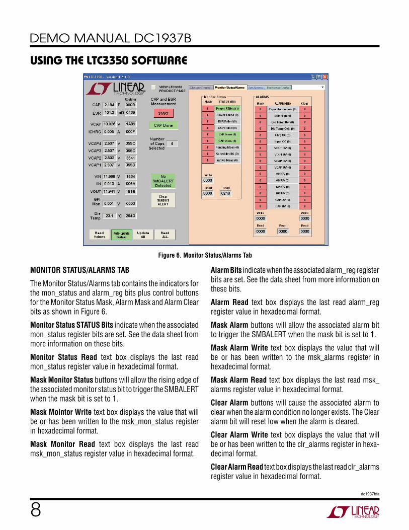
Figure 6. Monitor Status/Alarms Tab
MONITOR STATUS/ALARMS TAB
The Monitor Status/Alarms tab contains the indicators for the mon_status and alarm_reg bits plus control buttons for the Monitor Status Mask, Alarm Mask and Alarm Clear bits as shown in Figure 6.
Monitor Status STATUS Bits indicate when the associated mon_status register bits are set. See the data sheet from more information on these bits.
Monitor Status Read text box displays the last read mon_status register value in hexadecimal format.
Mask Monitor Status buttons will allow the rising edge of the associated monitor status bit to trigger the SMBALERT when the mask bit is set to 1.
Mask Mointor Write text box displays the value that will be or has been written to the msk_mon_status register in hexadecimal format.
Mask Monitor Read text box displays the last read msk_mon_status register value in hexadecimal format.
Alarm Bits indicate when the associated alarm_reg register bits are set. See the data sheet from more information on these bits.
Alarm Read text box displays the last read alarm_reg register value in hexadecimal format.
Mask Alarm buttons will allow the associated alarm bit to trigger the SMBALERT when the mask bit is set to 1.
Mask Alarm Write text box displays the value that will be or has been written to the msk_alarms register in hexadecimal format.
Mask Alarm Read text box displays the last read msk_alarms register value in hexadecimal format.
Clear Alarm buttons will cause the associated alarm to clear when the alarm condition no longer exists. The Clear alarm bit will reset low when the alarm is cleared.
Clear Alarm Write text box displays the value that will be or has been written to the clr_alarms register in hexa-decimal format.
Clear Alarm Read text box displays the last read clr_alarms register value in hexadecimal format.
usinG the ltc3350 softWare
9dc1937bfa
DEMO MANUAL DC1937B
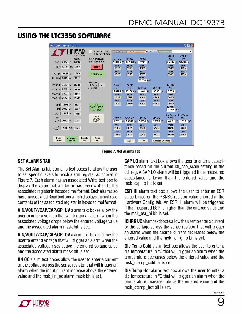
SET ALARMS TAB
The Set Alarms tab contains text boxes to allow the user to set specific levels for each alarm register as shown in Figure 7. Each alarm has an associated Write text box to display the value that will be or has been written to the associated register in hexadecimal format. Each alarm also has an associated Read text box which displays the last read contents of the associated register in hexadecimal format.
VIN/VOUT/VCAP/CAP/GPI UV alarm text boxes allow the user to enter a voltage that will trigger an alarm when the associated voltage drops below the entered voltage value and the associated alarm mask bit is set.
VIN/VOUT/VCAP/CAP/GPI OV alarm text boxes allow the user to enter a voltage that will trigger an alarm when the associated voltage rises above the entered voltage value and the associated alarm mask bit is set.
IIN OC alarm text boxes allow the user to enter a current or the voltage across the sense resistor that will trigger an alarm when the input current increase above the entered value and the msk_iin_oc alarm mask bit is set.
usinG the ltc3350 softWare
Figure 7. Set Alarms Tab
CAP LO alarm text box allows the user to enter a capaci-tance based on the current ctl_cap_scale setting in the ctl_reg. A CAP LO alarm will be triggered if the measured capacitance is lower than the entered value and the msk_cap_lo bit is set.
ESR HI alarm text box allows the user to enter an ESR value based on the RSNSC resistor value entered in the Hardware Config tab. An ESR HI alarm will be triggered if the measured ESR is higher than the entered value and the msk_esr_hi bit is set.
ICHRG UC alarm text boxes allow the user to enter a current or the voltage across the sense resistor that will trigger an alarm when the charge current decreases below the entered value and the msk_ichrg_lo bit is set.
Die Temp Cold alarm text box allows the user to enter a die temperature in °C that will trigger an alarm when the temperature decreases below the entered value and the msk_dtemp_cold bit is set.
Die Temp Hot alarm text box allows the user to enter a die temperature in °C that will trigger an alarm when the temperature increases above the entered value and the msk_dtemp_hot bit is set.
10dc1937bfa
DEMO MANUAL DC1937B
Figure 8. Hardware Config Tab
Apply button writes to all of the alarm registers and reads the values back from the LTC3350.
Cancel button changes all the entered values that have not yet been written to the LTC3350 back to their previ-ous values.
Restore Defaults button changes all of the LTC3350 alarm registers back to the default values determined from the GUI. This does not set the alarm to the LTC3350’s default settings of 0x0000.
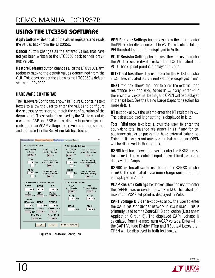
HARDWARE CONFIG TAB
The Hardware Config tab, shown in Figure 8, contains text boxes to allow the user to enter the values to configure the necessary resistors to match the configuration of the demo board. These values are used by the GUI to calculate measured CAP and ESR values, display input/charge cur-rents and max VCAP voltage for a given reference setting, and also used in the Set Alarm tab text boxes.
VPFI Resistor Settings text boxes allow the user to enter the PFI resistor divider network in kΩ. The calculated falling PFI threshold set point is displayed in Volts.
VOUT Resistor Settings text boxes allow the user to enter the VOUT resistor divider network in kΩ. The calculated VOUT backup set point is displayed in Volts.
RITST text box allows the user to enter the RITST resistor in Ω. The calculated test current setting is displayed in mA.
REXT text box allows the user to enter the external load resistance, R28 and R29, added in Ω if any. Enter –1 if there is not any external loading and OPEN will be displayed in the text box. See the Using Large Capacitor section for more details.
RT text box allows the user to enter the RT resistor in kΩ. The calculated oscillator setting is displayed in kHz.
Total RBalance text box allows the user to enter the equivalent total balance resistance in Ω if any for ca-pacitance stacks or packs that have external balancing. Enter –1 if there is not any external balancing and OPEN will be displayed in the text box.
RSNSI text box allows the user to enter the RSNSI resis-tor in mΩ. The calculated input current limit setting is displayed in Amps.
RSNSC text box allows the user to enter the RSNSC resistor in mΩ. The calculated maximum charge current setting is displayed in Amps.
VCAP Resistor Settings text boxes allow the user to enter the CAPFB resistor divider network in kΩ. The calculated maximum VCAP set point is displayed in Volts.
CAP1 Voltage Divider text boxes allow the user to enter the CAP1 resistor divider network in kΩ if used. This is primarily used for the Zeta/SEPIC application (Data sheet Application Circuit 6). The displayed CAP1 voltage is calculated from the maximum VCAP voltage. Enter –1 in the CAP1 Voltage Divider RTop and RBot text boxes then OPEN will be displayed in both text boxes.
usinG the ltc3350 softWare
11dc1937bfa
DEMO MANUAL DC1937B
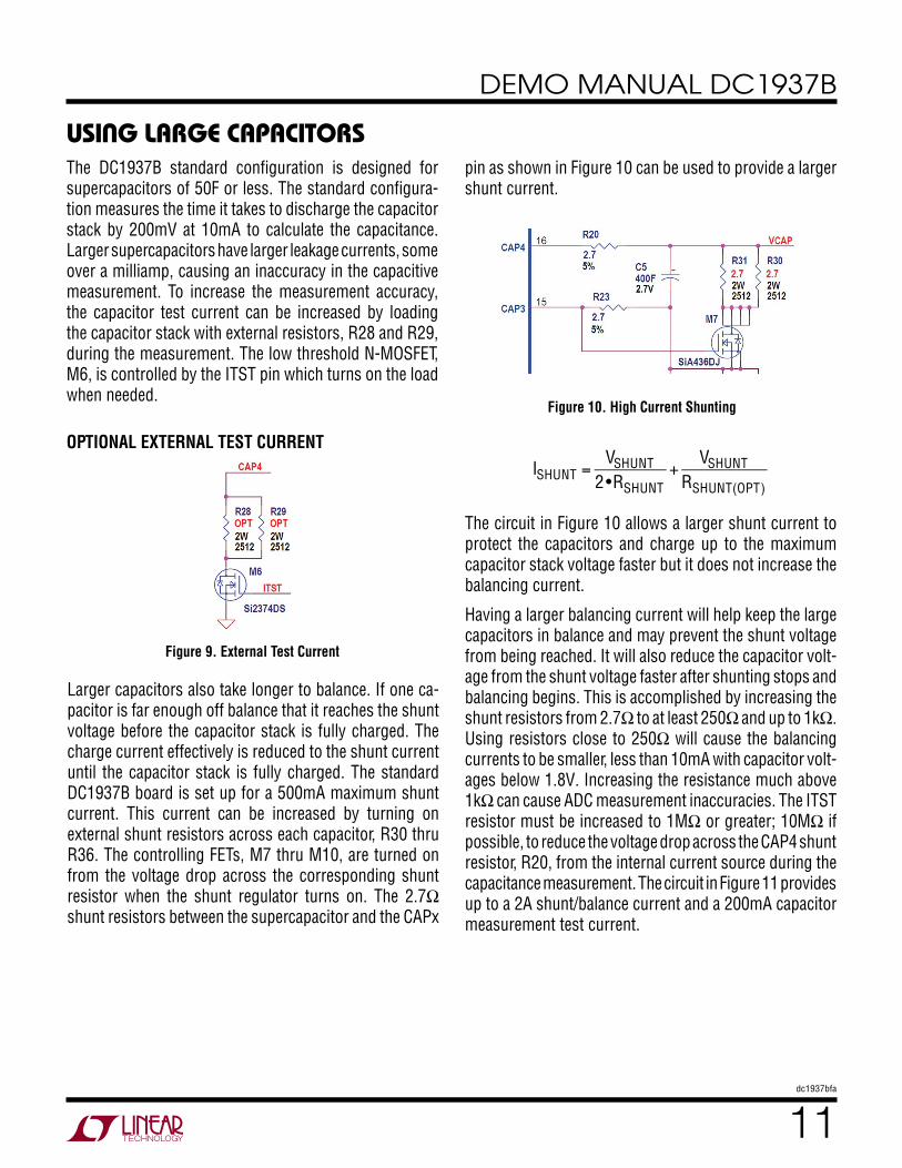
The DC1937B standard configuration is designed for supercapacitors of 50F or less. The standard configura-tion measures the time it takes to discharge the capacitor stack by 200mV at 10mA to calculate the capacitance. Larger supercapacitors have larger leakage currents, some over a milliamp, causing an inaccuracy in the capacitive measurement. To increase the measurement accuracy, the capacitor test current can be increased by loading the capacitor stack with external resistors, R28 and R29, during the measurement. The low threshold N-MOSFET, M6, is controlled by the ITST pin which turns on the load when needed.
OPTIONAL EXTERNAL TEST CURRENT
usinG larGe capacitors
Figure 9. External Test Current
Larger capacitors also take longer to balance. If one ca-pacitor is far enough off balance that it reaches the shunt voltage before the capacitor stack is fully charged. The charge current effectively is reduced to the shunt current until the capacitor stack is fully charged. The standard DC1937B board is set up for a 500mA maximum shunt current. This current can be increased by turning on external shunt resistors across each capacitor, R30 thru R36. The controlling FETs, M7 thru M10, are turned on from the voltage drop across the corresponding shunt resistor when the shunt regulator turns on. The 2.7Ω shunt resistors between the supercapacitor and the CAPx
pin as shown in Figure 10 can be used to provide a larger shunt current.
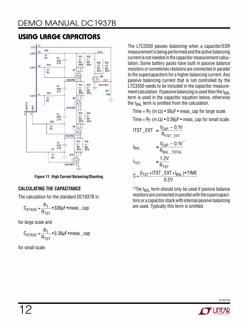
Figure 10. High Current Shunting
ISHUNT =
VSHUNT2 •RSHUNT
+VSHUNT
RSHUNT(OPT)
The circuit in Figure 10 allows a larger shunt current to protect the capacitors and charge up to the maximum capacitor stack voltage faster but it does not increase the balancing current.
Having a larger balancing current will help keep the large capacitors in balance and may prevent the shunt voltage from being reached. It will also reduce the capacitor volt-age from the shunt voltage faster after shunting stops and balancing begins. This is accomplished by increasing the shunt resistors from 2.7Ω to at least 250Ω and up to 1kΩ. Using resistors close to 250Ω will cause the balancing currents to be smaller, less than 10mA with capacitor volt-ages below 1.8V. Increasing the resistance much above 1kΩ can cause ADC measurement inaccuracies. The ITST resistor must be increased to 1MΩ or greater; 10MΩ if possible, to reduce the voltage drop across the CAP4 shunt resistor, R20, from the internal current source during the capacitance measurement. The circuit in Figure 11 provides up to a 2A shunt/balance current and a 200mA capacitor measurement test current.
12dc1937bfa
DEMO MANUAL DC1937B
usinG larGe capacitors
Figure 11. High Current Balancing/Shunting
CALCULATING THE CAPACITANCE
The calculation for the standard DC1937B is:
CSTACK =
RTRTST
•336µF •meas_cap
for large scale and
CSTACK =
RTRTST
•3.36µF •meas_cap
for small scale.
The LTC3350 pauses balancing when a capacitor/ESR measurement is being performed and the active balancing current is not needed in the capacitor measurement calcu-lation. Some battery packs have built in passive balance resistors or sometimes resistors are connected in parallel to the supercapacitors for a higher balancing current. Any passive balancing current that is not controlled by the LTC3350 needs to be included in the capacitor measure-ment calculation. If passive balancing is used then the IBAL term is used in the capacitor equation below, otherwise the IBAL term is omitted from the calculation.
Time = RT (in Ω) • 56µF • meas_cap for large scale.
Time = RT (in Ω) • 0.56µF • meas_cap for small scale.
ITST _EXT ≅VCAP – 0.1VRITST _EXT
IBAL ≅VCAP – 0.1VRBAL _ TOTAL
*
ITST ≅1.2VRTST
C=(ITST +ITST _EXT+IBAL )•TIME
0.2V
*The IBAL term should only be used if passive balance resistors are connected in parallel with the supercapaci-tors or a capacitor stack with internal passive balancing are used. Typically this term is omitted.
13dc1937bfa
DEMO MANUAL DC1937B
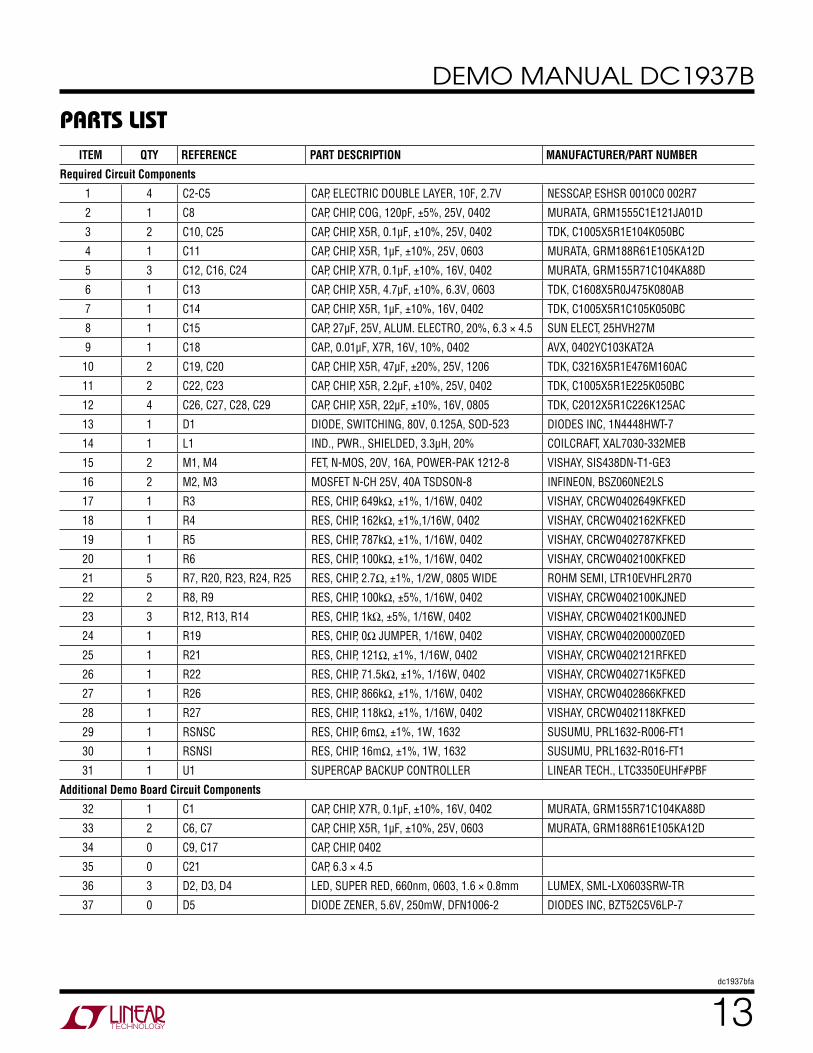
ITEM QTY REFERENCE PART DESCRIPTION MANUFACTURER/PART NUMBER
Required Circuit Components
1 4 C2-C5 CAP, ELECTRIC DOUBLE LAYER, 10F, 2.7V NESSCAP, ESHSR 0010C0 002R7
2 1 C8 CAP, CHIP, COG, 120pF, ±5%, 25V, 0402 MURATA, GRM1555C1E121JA01D
3 2 C10, C25 CAP, CHIP, X5R, 0.1µF, ±10%, 25V, 0402 TDK, C1005X5R1E104K050BC
4 1 C11 CAP, CHIP, X5R, 1µF, ±10%, 25V, 0603 MURATA, GRM188R61E105KA12D
5 3 C12, C16, C24 CAP, CHIP, X7R, 0.1µF, ±10%, 16V, 0402 MURATA, GRM155R71C104KA88D
6 1 C13 CAP, CHIP, X5R, 4.7µF, ±10%, 6.3V, 0603 TDK, C1608X5R0J475K080AB
7 1 C14 CAP, CHIP, X5R, 1µF, ±10%, 16V, 0402 TDK, C1005X5R1C105K050BC
8 1 C15 CAP, 27µF, 25V, ALUM. ELECTRO, 20%, 6.3 × 4.5 SUN ELECT, 25HVH27M
9 1 C18 CAP., 0.01μF, X7R, 16V, 10%, 0402 AVX, 0402YC103KAT2A
10 2 C19, C20 CAP, CHIP, X5R, 47µF, ±20%, 25V, 1206 TDK, C3216X5R1E476M160AC
11 2 C22, C23 CAP, CHIP, X5R, 2.2µF, ±10%, 25V, 0402 TDK, C1005X5R1E225K050BC
12 4 C26, C27, C28, C29 CAP, CHIP, X5R, 22μF, ±10%, 16V, 0805 TDK, C2012X5R1C226K125AC
13 1 D1 DIODE, SWITCHING, 80V, 0.125A, SOD-523 DIODES INC, 1N4448HWT-7
14 1 L1 IND., PWR., SHIELDED, 3.3μH, 20% COILCRAFT, XAL7030-332MEB
15 2 M1, M4 FET, N-MOS, 20V, 16A, POWER-PAK 1212-8 VISHAY, SIS438DN-T1-GE3
16 2 M2, M3 MOSFET N-CH 25V, 40A TSDSON-8 INFINEON, BSZ060NE2LS
17 1 R3 RES, CHIP, 649kΩ, ±1%, 1/16W, 0402 VISHAY, CRCW0402649KFKED
18 1 R4 RES, CHIP, 162kΩ, ±1%,1/16W, 0402 VISHAY, CRCW0402162KFKED
19 1 R5 RES, CHIP, 787kΩ, ±1%, 1/16W, 0402 VISHAY, CRCW0402787KFKED
20 1 R6 RES, CHIP, 100kΩ, ±1%, 1/16W, 0402 VISHAY, CRCW0402100KFKED
21 5 R7, R20, R23, R24, R25 RES, CHIP, 2.7Ω, ±1%, 1/2W, 0805 WIDE ROHM SEMI, LTR10EVHFL2R70
22 2 R8, R9 RES, CHIP, 100kΩ, ±5%, 1/16W, 0402 VISHAY, CRCW0402100KJNED
23 3 R12, R13, R14 RES, CHIP, 1kΩ, ±5%, 1/16W, 0402 VISHAY, CRCW04021K00JNED
24 1 R19 RES, CHIP, 0Ω JUMPER, 1/16W, 0402 VISHAY, CRCW04020000Z0ED
25 1 R21 RES, CHIP, 121Ω, ±1%, 1/16W, 0402 VISHAY, CRCW0402121RFKED
26 1 R22 RES, CHIP, 71.5kΩ, ±1%, 1/16W, 0402 VISHAY, CRCW040271K5FKED
27 1 R26 RES, CHIP, 866kΩ, ±1%, 1/16W, 0402 VISHAY, CRCW0402866KFKED
28 1 R27 RES, CHIP, 118kΩ, ±1%, 1/16W, 0402 VISHAY, CRCW0402118KFKED
29 1 RSNSC RES, CHIP, 6mΩ, ±1%, 1W, 1632 SUSUMU, PRL1632-R006-FT1
30 1 RSNSI RES, CHIP, 16mΩ, ±1%, 1W, 1632 SUSUMU, PRL1632-R016-FT1
31 1 U1 SUPERCAP BACKUP CONTROLLER LINEAR TECH., LTC3350EUHF#PBF
Additional Demo Board Circuit Components
32 1 C1 CAP, CHIP, X7R, 0.1µF, ±10%, 16V, 0402 MURATA, GRM155R71C104KA88D
33 2 C6, C7 CAP, CHIP, X5R, 1µF, ±10%, 25V, 0603 MURATA, GRM188R61E105KA12D
34 0 C9, C17 CAP, CHIP, 0402
35 0 C21 CAP, 6.3 × 4.5
36 3 D2, D3, D4 LED, SUPER RED, 660nm, 0603, 1.6 × 0.8mm LUMEX, SML-LX0603SRW-TR
37 0 D5 DIODE ZENER, 5.6V, 250mW, DFN1006-2 DIODES INC, BZT52C5V6LP-7
parts list
14dc1937bfa
DEMO MANUAL DC1937B
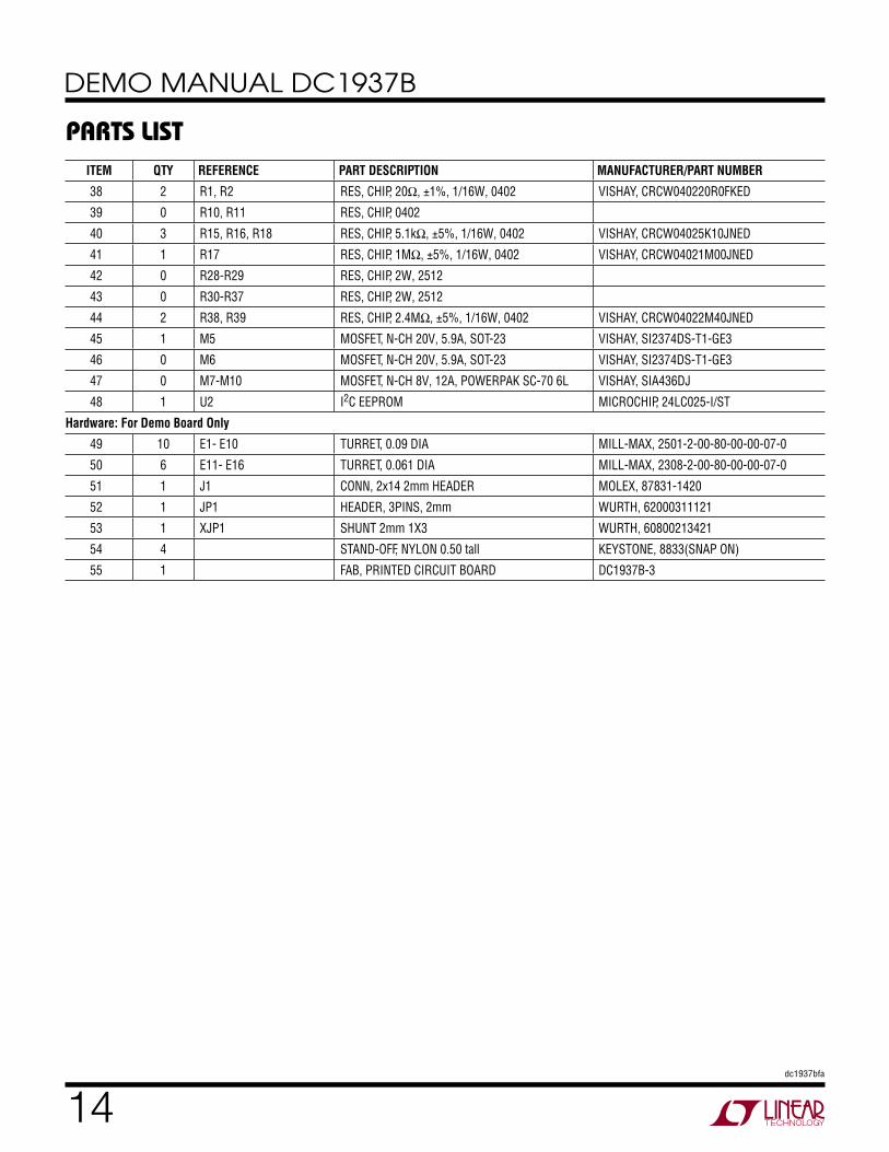
parts listITEM QTY REFERENCE PART DESCRIPTION MANUFACTURER/PART NUMBER
38 2 R1, R2 RES, CHIP, 20Ω, ±1%, 1/16W, 0402 VISHAY, CRCW040220R0FKED
39 0 R10, R11 RES, CHIP, 0402
40 3 R15, R16, R18 RES, CHIP, 5.1kΩ, ±5%, 1/16W, 0402 VISHAY, CRCW04025K10JNED
41 1 R17 RES, CHIP, 1MΩ, ±5%, 1/16W, 0402 VISHAY, CRCW04021M00JNED
42 0 R28-R29 RES, CHIP, 2W, 2512
43 0 R30-R37 RES, CHIP, 2W, 2512
44 2 R38, R39 RES, CHIP, 2.4MΩ, ±5%, 1/16W, 0402 VISHAY, CRCW04022M40JNED
45 1 M5 MOSFET, N-CH 20V, 5.9A, SOT-23 VISHAY, SI2374DS-T1-GE3
46 0 M6 MOSFET, N-CH 20V, 5.9A, SOT-23 VISHAY, SI2374DS-T1-GE3
47 0 M7-M10 MOSFET, N-CH 8V, 12A, POWERPAK SC-70 6L VISHAY, SIA436DJ
48 1 U2 I2C EEPROM MICROCHIP, 24LC025-I/ST
Hardware: For Demo Board Only
49 10 E1- E10 TURRET, 0.09 DIA MILL-MAX, 2501-2-00-80-00-00-07-0
50 6 E11- E16 TURRET, 0.061 DIA MILL-MAX, 2308-2-00-80-00-00-07-0
51 1 J1 CONN, 2x14 2mm HEADER MOLEX, 87831-1420
52 1 JP1 HEADER, 3PINS, 2mm WURTH, 62000311121
53 1 XJP1 SHUNT 2mm 1X3 WURTH, 60800213421
54 4 STAND-OFF, NYLON 0.50 tall KEYSTONE, 8833(SNAP ON)
55 1 FAB, PRINTED CIRCUIT BOARD DC1937B-3
15dc1937bfa
DEMO MANUAL DC1937B5 5
4 4
3 3
2 2
1 1
DD
CC
BB
AA
6V B
ACKU
P10
.8V
- 20V
10.8
V - 2
0V
UNLE
SS N
OTED
:RE
SIST
ORS:
OHM
S, 0
402,
1%
, 1/1
6WCA
PACI
TORS
: uF
, 040
2, 6
.3V,
10%
12V
NOM
INAL
25W
X5R
X5R
X5R
X5R
25W
DC59
0IN
TVCC
PULL
- UP
P
WR
OPT
0508
0508
0508
0508
0508
OPTI
ONAL
EXT
ERNA
LTE
ST C
URRE
NTOP
TION
AL E
XTER
NAL
SHUN
T CU
RREN
T
R38
AND
R39
ARE
FOR
STAN
D-AL
ONE
OPER
ATIO
N ON
LYAN
D TH
E I2
C BU
S IS
NOT
USE
D.
SMBUSALERT
ITST
ITST
GCAP
4GC
AP3
GCAP
2GC
AP1
CAP1
CAP4
CAP4
CAP3
CAP2
CAP3
CAP1
CAP1
CAP2
CAP3
CAP4
GCAP
1
GCAP
2
GCAP
3
GCAP
4
CAP2
VCC
VCC
INTV
CC
INTV
CC
REVI
SION
HIS
TORY
DESC
RIPT
ION
DATE
APPR
OVED
ECO
REV
MM
PROD
UCTI
ON F
AB-
305
-04-
15
REVI
SION
HIS
TORY
DESC
RIPT
ION
DATE
APPR
OVED
ECO
REV
MM
PROD
UCTI
ON F
AB-
305
-04-
15
REVI
SION
HIS
TORY
DESC
RIPT
ION
DATE
APPR
OVED
ECO
REV
MM
PROD
UCTI
ON F
AB-
305
-04-
15
SIZE
DATE
:
IC N
O.RE
V.
SHEE
TOF
TITL
E:
APPR
OVAL
S
PCB
DES.
APP
ENG.
TECHNOLO
GY
Fax:
(408
)434
-050
7
Milp
itas,
CA 95
035
Phon
e: (4
08)4
32-1
900
1630
McC
arth
y Blvd
.
LTC
Conf
iden
tial-F
or C
usto
mer
Use
Onl
y
CUST
OMER
NOT
ICE
LINE
AR T
ECHN
OLOG
Y HA
S MA
DE A
BES
T EF
FORT
TO
DESI
GN A
CIRC
UIT
THAT
MEE
TS C
USTO
MER-
SUPP
LIED
SPE
CIFI
CATI
ONS;
HOW
EVER
, IT R
EMAI
NS T
HE C
USTO
MER'
S RE
SPON
SIBI
LITY
TO
VERI
FY P
ROPE
R AN
D RE
LIAB
LE O
PERA
TION
IN T
HE A
CTUA
LAP
PLIC
ATIO
N. C
OMPO
NENT
SUB
STIT
UTIO
N AN
D PR
INTE
DCI
RCUI
T BO
ARD
LAYO
UT M
AY S
IGNI
FICA
NTLY
AFF
ECT
CIRC
UIT
PERF
ORMA
NCE
OR R
ELIA
BILI
TY. C
ONTA
CT L
INEA
RTE
CHNO
LOGY
APP
LICA
TION
S EN
GINE
ERIN
G FO
R AS
SIST
ANCE
.
THIS
CIR
CUIT
IS P
ROPR
IETA
RY T
O LI
NEAR
TEC
HNOL
OGY
AND
SCHE
MAT
IC
SUPP
LIED
FOR
USE
WIT
H LI
NEAR
TEC
HNOL
OGY
PART
S.SC
ALE
= NO
NE
www.
linea
r.com 3
DEM
O CI
RCUI
T 19
37B
11
HIGH
CUR
RENT
SUP
ERCA
PACI
TOR
N/A
LTC3
350E
UHF
NC MM
BACK
UP C
ONTR
OLLE
R AN
D SY
STEM
MON
ITOR
05 -
04 -
15
RSNS
C0.
006
PRL1
632
U2 24LC
025-
I/ST
A01
SCLK
6
A23
VSS 4
SDA
5
A12
WP
7
VCC8
C26
22uF
0805
16V
10%
E3
VOUT
R10
OPT
D SG
M3
BSZ0
60NE
2LS
7
4
123
68
5R1
85.1
K5%
E7CA
P1
C28
22uF
0805
16V
10%
D SG
M2
BSZ0
60NE
2LS
7
4
123
68
5
C20
47uF
1206
25V
20%
M6
Si23
74DS
R25
2.7
5%
R35
OPT
2W 2512
R27
118K
+C1
527
uF25
HVH2
7M25
V20
%
R31
OPT
2W 2512
R22
71.5
K
R6 100K
R29
OPT
2W 2512
M5
Si23
74DS
E12
CAPG
D
C29
22uF
0805
16V
10%
+C3 10
F2.7
V
R36
OPT
2W 2512
TPA2
C17
OPT
R38
2.4M
5%
M9 Si
A436
DJ
R21
121
M7
SiA4
36DJ
R13
1K 5%
C14
1uF
16V
5.6V
D5 BZT5
2C5V
6LP
R33
OPT
2W 2512
C1 0.1uF
16V
C23
2.2u
F25
V
R11
OPT
E14
GND
+C2 10
F2.7
V
TPB2
E1VI
N
C24
0.1u
F16
V
R26
866K
R39
2.4M
5%
R19 0
C12
0.1u
F16
VR8 10
0K5%
E13
PFO
C25
0.1u
F25
V
M8
SiA4
36DJ
TPB1
C6 1uF
0603
25V
L1 3.3u
HXA
L703
0-33
2MEB
C18
10nF
16V
R16
5.1K
5%
R14
1K 5%
+C5 10
F2.7
V
D2 PFO
RED
C22
2.2u
F25
V
JP1
+C2
1OP
T6.3
DIA
C19
47uF
1206
25V
20%
C13
4.7u
F06
03
M10
SiA4
36DJ
C11
1uF
0603
25V
D
SG
M1
SiS4
38DN7
4
12368 5
RSNS
I0.
016
PRL1
632
R1 20
R37
OPT
2W 2512
D4 SMBA
LERT
RED
E11
SMBA
LERT
D SG
M4
SiS4
38DN
7
4
123
6
8
5
E9VC
AP10
V
R12
1K 5%
E16
GPI
R20
2.7
5%
TP2
SCL
R7 2.7
5%
D1 1N44
48HW
TSO
D-52
3
+C4 10
F2.7
V
U1 LTC3
350E
UHF
VCAP
21
PFI
37
CAP_
SLCT
136
PFO 38
PGND 39CF
P17
CFN
18
BST
26
BGAT
E27
SMBALERT 3
CAPFB 6
OUTFB7
SGND
8
RT9
INFET33
VOUTSN30
VOUTSP31
VOUTM532
VIN34
SCL
1
SDA
2
ICAP
22
VCC2
P523
SW24
TGAT
E25
CAP2
14
CAP3
15
CAP4
16
CAP_
SLCT
035
VCAP
P519
OUTFET20
INTV
CC29
DRVC
C28
CAPGD 4
VC5
GPI
10
ITST
11
CAPRTN 12
CAP1
13
R34
OPT
2W 2512
R2 20D3 CA
PGD
RED
J1 HD2X
7
+1
+3
+5
+7
+9
+11
+13
+2
+4
+6
+8
+10
+12
+14
R30
OPT
2W 2512
E5CA
P3
TP1
SDA
R9 100K
5%
E10
GND
E4GN
D
R15
5.1K
5%
R578
7K
R23
2.7
5%
C7 1uF
0603
25V
R4 162K
E15
GND
E8GN
D
C27
22uF
0805
16V
10%
E2GN
D
R28
OPT
2W 2512
E6CA
P2
C9 OPT
TPA1
R32
OPT
2W 2512
C16
0.1u
F16
V
R24
2.7
5%
R17
1M 5%
C10
0.1u
F25
V
R3 649K
C8 120p
F25
V5%
Information furnished by Linear Technology Corporation is believed to be accurate and reliable. However, no responsibility is assumed for its use. Linear Technology Corporation makes no representa-tion that the interconnection of its circuits as described herein will not infringe on existing patent rights.
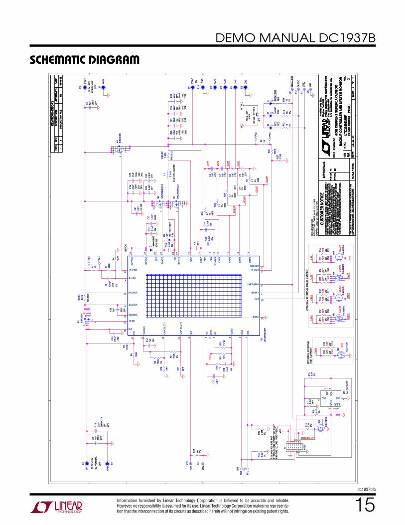
schematic DiaGram
16dc1937bfa
DEMO MANUAL DC1937B
Linear Technology Corporation1630 McCarthy Blvd., Milpitas, CA 95035-7417 (408) 432-1900 FAX: (408) 434-0507 www.linear.com LINEAR TECHNOLOGY CORPORATION 2015
LT 1215 REV A • PRINTED IN USA
DEMONSTRATION BOARD IMPORTANT NOTICE
Linear Technology Corporation (LTC) provides the enclosed product(s) under the following AS IS conditions:
This demonstration board (DEMO BOARD) kit being sold or provided by Linear Technology is intended for use for ENGINEERING DEVELOPMENT OR EVALUATION PURPOSES ONLY and is not provided by LTC for commercial use. As such, the DEMO BOARD herein may not be complete in terms of required design-, marketing-, and/or manufacturing-related protective considerations, including but not limited to product safety measures typically found in finished commercial goods. As a prototype, this product does not fall within the scope of the European Union directive on electromagnetic compatibility and therefore may or may not meet the technical requirements of the directive, or other regulations.
If this evaluation kit does not meet the specifications recited in the DEMO BOARD manual the kit may be returned within 30 days from the date of delivery for a full refund. THE FOREGOING WARRANTY IS THE EXCLUSIVE WARRANTY MADE BY THE SELLER TO BUYER AND IS IN LIEU OF ALL OTHER WARRANTIES, EXPRESSED, IMPLIED, OR STATUTORY, INCLUDING ANY WARRANTY OF MERCHANTABILITY OR FITNESS FOR ANY PARTICULAR PURPOSE. EXCEPT TO THE EXTENT OF THIS INDEMNITY, NEITHER PARTY SHALL BE LIABLE TO THE OTHER FOR ANY INDIRECT, SPECIAL, INCIDENTAL, OR CONSEQUENTIAL DAMAGES.
The user assumes all responsibility and liability for proper and safe handling of the goods. Further, the user releases LTC from all claims arising from the handling or use of the goods. Due to the open construction of the product, it is the user’s responsibility to take any and all appropriate precautions with regard to electrostatic discharge. Also be aware that the products herein may not be regulatory compliant or agency certified (FCC, UL, CE, etc.).
No License is granted under any patent right or other intellectual property whatsoever. LTC assumes no liability for applications assistance, customer product design, software performance, or infringement of patents or any other intellectual property rights of any kind.
LTC currently services a variety of customers for products around the world, and therefore this transaction is not exclusive.
Please read the DEMO BOARD manual prior to handling the product. Persons handling this product must have electronics training and observe good laboratory practice standards. Common sense is encouraged.
This notice contains important safety information about temperatures and voltages. For further safety concerns, please contact a LTC application engineer.
Mailing Address:
Linear Technology
1630 McCarthy Blvd.
Milpitas, CA 95035
Copyright © 2004, Linear Technology Corporation